EP2044632B1 - Pile solaire présentant une zone de diffusion de base réduite - Google Patents
Pile solaire présentant une zone de diffusion de base réduite Download PDFInfo
- Publication number
- EP2044632B1 EP2044632B1 EP07809355.6A EP07809355A EP2044632B1 EP 2044632 B1 EP2044632 B1 EP 2044632B1 EP 07809355 A EP07809355 A EP 07809355A EP 2044632 B1 EP2044632 B1 EP 2044632B1
- Authority
- EP
- European Patent Office
- Prior art keywords
- solar cell
- base diffusion
- diffusion regions
- diffusion region
- metal grid
- Prior art date
- Legal status (The legal status is an assumption and is not a legal conclusion. Google has not performed a legal analysis and makes no representation as to the accuracy of the status listed.)
- Active
Links
- 238000009792 diffusion process Methods 0.000 title claims description 172
- 239000002800 charge carrier Substances 0.000 claims description 57
- 239000002184 metal Substances 0.000 claims description 51
- 239000012212 insulator Substances 0.000 claims description 35
- 238000000034 method Methods 0.000 claims description 27
- XUIMIQQOPSSXEZ-UHFFFAOYSA-N Silicon Chemical compound [Si] XUIMIQQOPSSXEZ-UHFFFAOYSA-N 0.000 claims description 13
- 239000002019 doping agent Substances 0.000 claims description 13
- 229910052710 silicon Inorganic materials 0.000 claims description 13
- 239000010703 silicon Substances 0.000 claims description 13
- 238000004519 manufacturing process Methods 0.000 claims description 12
- 239000000758 substrate Substances 0.000 claims description 9
- VYPSYNLAJGMNEJ-UHFFFAOYSA-N Silicium dioxide Chemical compound O=[Si]=O VYPSYNLAJGMNEJ-UHFFFAOYSA-N 0.000 claims description 8
- 235000012239 silicon dioxide Nutrition 0.000 claims description 4
- 239000000377 silicon dioxide Substances 0.000 claims description 4
- ZOXJGFHDIHLPTG-UHFFFAOYSA-N Boron Chemical compound [B] ZOXJGFHDIHLPTG-UHFFFAOYSA-N 0.000 claims description 2
- OAICVXFJPJFONN-UHFFFAOYSA-N Phosphorus Chemical compound [P] OAICVXFJPJFONN-UHFFFAOYSA-N 0.000 claims description 2
- 229910052796 boron Inorganic materials 0.000 claims description 2
- 229910052698 phosphorus Inorganic materials 0.000 claims description 2
- 239000011574 phosphorus Substances 0.000 claims description 2
- 239000011295 pitch Substances 0.000 description 16
- 238000005215 recombination Methods 0.000 description 16
- 230000006798 recombination Effects 0.000 description 16
- 238000000059 patterning Methods 0.000 description 5
- 230000007246 mechanism Effects 0.000 description 4
- 238000005516 engineering process Methods 0.000 description 3
- 238000007639 printing Methods 0.000 description 3
- 238000007650 screen-printing Methods 0.000 description 3
- 239000004065 semiconductor Substances 0.000 description 3
- 238000007641 inkjet printing Methods 0.000 description 2
- 230000005855 radiation Effects 0.000 description 2
- 239000004642 Polyimide Substances 0.000 description 1
- 230000002411 adverse Effects 0.000 description 1
- 239000010953 base metal Substances 0.000 description 1
- 230000009286 beneficial effect Effects 0.000 description 1
- 230000015572 biosynthetic process Effects 0.000 description 1
- 230000003247 decreasing effect Effects 0.000 description 1
- 230000007547 defect Effects 0.000 description 1
- 230000001419 dependent effect Effects 0.000 description 1
- 230000000694 effects Effects 0.000 description 1
- 238000010292 electrical insulation Methods 0.000 description 1
- 238000002347 injection Methods 0.000 description 1
- 239000007924 injection Substances 0.000 description 1
- 238000009413 insulation Methods 0.000 description 1
- 238000005457 optimization Methods 0.000 description 1
- 230000000737 periodic effect Effects 0.000 description 1
- 238000000206 photolithography Methods 0.000 description 1
- 229920001721 polyimide Polymers 0.000 description 1
Images


Classifications
-
- H—ELECTRICITY
- H01—ELECTRIC ELEMENTS
- H01L—SEMICONDUCTOR DEVICES NOT COVERED BY CLASS H10
- H01L31/00—Semiconductor devices sensitive to infrared radiation, light, electromagnetic radiation of shorter wavelength or corpuscular radiation and specially adapted either for the conversion of the energy of such radiation into electrical energy or for the control of electrical energy by such radiation; Processes or apparatus specially adapted for the manufacture or treatment thereof or of parts thereof; Details thereof
- H01L31/04—Semiconductor devices sensitive to infrared radiation, light, electromagnetic radiation of shorter wavelength or corpuscular radiation and specially adapted either for the conversion of the energy of such radiation into electrical energy or for the control of electrical energy by such radiation; Processes or apparatus specially adapted for the manufacture or treatment thereof or of parts thereof; Details thereof adapted as photovoltaic [PV] conversion devices
-
- H—ELECTRICITY
- H01—ELECTRIC ELEMENTS
- H01L—SEMICONDUCTOR DEVICES NOT COVERED BY CLASS H10
- H01L31/00—Semiconductor devices sensitive to infrared radiation, light, electromagnetic radiation of shorter wavelength or corpuscular radiation and specially adapted either for the conversion of the energy of such radiation into electrical energy or for the control of electrical energy by such radiation; Processes or apparatus specially adapted for the manufacture or treatment thereof or of parts thereof; Details thereof
- H01L31/02—Details
- H01L31/0224—Electrodes
- H01L31/022408—Electrodes for devices characterised by at least one potential jump barrier or surface barrier
- H01L31/022425—Electrodes for devices characterised by at least one potential jump barrier or surface barrier for solar cells
- H01L31/022441—Electrode arrangements specially adapted for back-contact solar cells
-
- H—ELECTRICITY
- H01—ELECTRIC ELEMENTS
- H01L—SEMICONDUCTOR DEVICES NOT COVERED BY CLASS H10
- H01L31/00—Semiconductor devices sensitive to infrared radiation, light, electromagnetic radiation of shorter wavelength or corpuscular radiation and specially adapted either for the conversion of the energy of such radiation into electrical energy or for the control of electrical energy by such radiation; Processes or apparatus specially adapted for the manufacture or treatment thereof or of parts thereof; Details thereof
- H01L31/04—Semiconductor devices sensitive to infrared radiation, light, electromagnetic radiation of shorter wavelength or corpuscular radiation and specially adapted either for the conversion of the energy of such radiation into electrical energy or for the control of electrical energy by such radiation; Processes or apparatus specially adapted for the manufacture or treatment thereof or of parts thereof; Details thereof adapted as photovoltaic [PV] conversion devices
- H01L31/06—Semiconductor devices sensitive to infrared radiation, light, electromagnetic radiation of shorter wavelength or corpuscular radiation and specially adapted either for the conversion of the energy of such radiation into electrical energy or for the control of electrical energy by such radiation; Processes or apparatus specially adapted for the manufacture or treatment thereof or of parts thereof; Details thereof adapted as photovoltaic [PV] conversion devices characterised by at least one potential-jump barrier or surface barrier
- H01L31/061—Semiconductor devices sensitive to infrared radiation, light, electromagnetic radiation of shorter wavelength or corpuscular radiation and specially adapted either for the conversion of the energy of such radiation into electrical energy or for the control of electrical energy by such radiation; Processes or apparatus specially adapted for the manufacture or treatment thereof or of parts thereof; Details thereof adapted as photovoltaic [PV] conversion devices characterised by at least one potential-jump barrier or surface barrier the potential barriers being of the point-contact type
-
- H—ELECTRICITY
- H01—ELECTRIC ELEMENTS
- H01L—SEMICONDUCTOR DEVICES NOT COVERED BY CLASS H10
- H01L31/00—Semiconductor devices sensitive to infrared radiation, light, electromagnetic radiation of shorter wavelength or corpuscular radiation and specially adapted either for the conversion of the energy of such radiation into electrical energy or for the control of electrical energy by such radiation; Processes or apparatus specially adapted for the manufacture or treatment thereof or of parts thereof; Details thereof
- H01L31/04—Semiconductor devices sensitive to infrared radiation, light, electromagnetic radiation of shorter wavelength or corpuscular radiation and specially adapted either for the conversion of the energy of such radiation into electrical energy or for the control of electrical energy by such radiation; Processes or apparatus specially adapted for the manufacture or treatment thereof or of parts thereof; Details thereof adapted as photovoltaic [PV] conversion devices
- H01L31/06—Semiconductor devices sensitive to infrared radiation, light, electromagnetic radiation of shorter wavelength or corpuscular radiation and specially adapted either for the conversion of the energy of such radiation into electrical energy or for the control of electrical energy by such radiation; Processes or apparatus specially adapted for the manufacture or treatment thereof or of parts thereof; Details thereof adapted as photovoltaic [PV] conversion devices characterised by at least one potential-jump barrier or surface barrier
- H01L31/068—Semiconductor devices sensitive to infrared radiation, light, electromagnetic radiation of shorter wavelength or corpuscular radiation and specially adapted either for the conversion of the energy of such radiation into electrical energy or for the control of electrical energy by such radiation; Processes or apparatus specially adapted for the manufacture or treatment thereof or of parts thereof; Details thereof adapted as photovoltaic [PV] conversion devices characterised by at least one potential-jump barrier or surface barrier the potential barriers being only of the PN homojunction type, e.g. bulk silicon PN homojunction solar cells or thin film polycrystalline silicon PN homojunction solar cells
- H01L31/0682—Semiconductor devices sensitive to infrared radiation, light, electromagnetic radiation of shorter wavelength or corpuscular radiation and specially adapted either for the conversion of the energy of such radiation into electrical energy or for the control of electrical energy by such radiation; Processes or apparatus specially adapted for the manufacture or treatment thereof or of parts thereof; Details thereof adapted as photovoltaic [PV] conversion devices characterised by at least one potential-jump barrier or surface barrier the potential barriers being only of the PN homojunction type, e.g. bulk silicon PN homojunction solar cells or thin film polycrystalline silicon PN homojunction solar cells back-junction, i.e. rearside emitter, solar cells, e.g. interdigitated base-emitter regions back-junction cells
-
- H—ELECTRICITY
- H01—ELECTRIC ELEMENTS
- H01L—SEMICONDUCTOR DEVICES NOT COVERED BY CLASS H10
- H01L31/00—Semiconductor devices sensitive to infrared radiation, light, electromagnetic radiation of shorter wavelength or corpuscular radiation and specially adapted either for the conversion of the energy of such radiation into electrical energy or for the control of electrical energy by such radiation; Processes or apparatus specially adapted for the manufacture or treatment thereof or of parts thereof; Details thereof
- H01L31/18—Processes or apparatus specially adapted for the manufacture or treatment of these devices or of parts thereof
-
- Y—GENERAL TAGGING OF NEW TECHNOLOGICAL DEVELOPMENTS; GENERAL TAGGING OF CROSS-SECTIONAL TECHNOLOGIES SPANNING OVER SEVERAL SECTIONS OF THE IPC; TECHNICAL SUBJECTS COVERED BY FORMER USPC CROSS-REFERENCE ART COLLECTIONS [XRACs] AND DIGESTS
- Y02—TECHNOLOGIES OR APPLICATIONS FOR MITIGATION OR ADAPTATION AGAINST CLIMATE CHANGE
- Y02E—REDUCTION OF GREENHOUSE GAS [GHG] EMISSIONS, RELATED TO ENERGY GENERATION, TRANSMISSION OR DISTRIBUTION
- Y02E10/00—Energy generation through renewable energy sources
- Y02E10/50—Photovoltaic [PV] energy
- Y02E10/547—Monocrystalline silicon PV cells
Definitions
- the present invention relates generally to solar cells, and more particularly but not exclusively to solar cell structures.
- US 2002/0046765 A1 relates to a photovoltaic cell and a process for producing the same.
- Solar cells are well known devices for converting solar radiation to electrical energy. They may be fabricated on a semiconductor wafer using semiconductor processing technology. Generally speaking, a solar cell may be fabricated by forming P-type and N-type diffusion regions in a silicon substrate. Solar radiation impinging on the solar cell creates electrons and holes that migrate to the diffusion regions, thereby creating voltage differentials between the diffusion regions. In a back side contact solar cell, both the diffusion regions and the metal grids coupled to them are on the back side of the solar cell. The metal grids allow an external electrical circuit to be coupled to and be powered by the solar cell. Back side contact solar cells are also disclosed in U.S. Pat. Nos. 5,053,083 and 4,927,770 . for increasing the efficiency of solar cells are generally desirable. The present invention discloses improved back side contact cell structures that allow for higher efficiency compared to conventional solar cells.
- the present invention relates to a method of fabricating a solar cell according to claim 1. Further advantageous embodiments are defined in the dependent claims.
- a solar cell has base and emitter diffusion regions formed on the back side.
- the emitter diffusion region is configured to collect minority charge carriers in the solar cell, while the base diffusion region is configured to collect majority charge carriers.
- the emitter diffusion region may be a continuous region separating the base diffusion regions.
- Each of the base diffusion regions may have a reduced area to decrease minority charge carrier recombination losses without substantially increasing series resistance losses due to lateral flow of majority charge carriers.
- Each of the base diffusion regions may have a dot shape, for example.
- the present disclosure relates to the fabrication of solar cells.
- Solar cell fabrication processes are also disclosed in the following commonly-assigned disclosures U.S. Publication number US 7339110 (Application No. 10/412,638 ), entitled “Improved Solar Cell and Method of Manufacture,” filed on April 10, 2003 by William P. Mulligan, Michael J. Cudzinovic, Thomas Pass, David Smith, Neil Kaminar, Keith McIntosh, and Richard M. Swanson; U.S. Publication No. 2004/0200520 (application no. 10/412,711 ), entitled “Metal Contact Structure For Solar Cell And Method Of Manufacture,” filed on April 10, 2003 by William P. Mulligan, Michael J. Cudzinovic, Thomas Pass, David Smith, and Richard M. Swanson; and U.S. Patent No. 6,998,288 issued to Smith et al.
- minority charge carriers are collected in the emitter diffusion regions of the solar cell and majority charge carriers are collected in the base diffusion regions.
- the minority charge carriers are collected by the P-type diffusion region (the “emitter diffusion region” in this case), and in turn are conducted through a metal grid to the positive terminal.
- the majority charge carriers are collected by the N-type diffusion (the “base diffusion region” in this case), and in turn are conducted by a metal grid to the negative terminal.
- carrier path length is a key parameter in determining the performance of a back side contact solar cell.
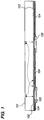
- FIG. 1 shows a cross-section of an example back side contact solar cell, schematically illustrating lateral transport of charge carriers.
- the solar cell comprises a wafer 101 having a base diffusion region 102 and an emitter diffusion region 103 on the back side thereof.
- a base metal finger 105 allows for external electrical connection to the base diffusion region 102, while an emitter metal finger 106 allows for external electrical connection to the emitter diffusion region.
- An insulation layer 104 is formed over the diffusion regions.
- the wafer 101 is an N-type silicon wafer having a thickness of about 0.200 mm, and the pitch of the diffusion regions is about 2.000 mm.
- the filled circles represent electrons, which are the majority charge carriers in this example.
- the empty circles represent holes, which are the minority charge carriers in this example.
- the dash lines represent charge carrier travel paths in the wafer 101.
- the lateral transport of minority and majority charge carriers introduces two undesirable loss mechanisms to back side contact solar cells: (a) increased minority charge carrier recombination from lateral minority charge carrier transport and (b) increased series resistance from lateral majority charge carrier transport. Because the pitch is several times larger than thickness of the wafer in the example of FIG. 1 , the lateral transport of the charge carriers, and thus the losses associated with it, becomes significant.
- FIG. 2 shows vertical transport of charge carriers in the solar cell of FIG. 1 if the pitch of the diffusion regions was made smaller than the thickness of the wafer 101.
- the solar cells of FIGS. 1 and 2 are the same except for the thickness of the wafer 101 and the pitch of the diffusion regions.
- the wafer 101 is 0.150 mm thick and the pitch of the diffusion regions is about 0.050 mm.
- the filled circles represent electrons, which are the majority charge carriers in this example.
- the empty circles represent holes, which are the minority charge carriers in this example.
- the dash lines represent the charge carrier travel paths in the wafer 101.
- the other components of FIG. 2 have been previously discussed with reference to FIG. 1 .
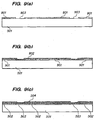
- the first is the point diffusions typically used for concentrator systems (e.g., see “ An Optimization Study of Point-Contact Concentrator Solar Cells", R.A. Sinton and R.M. Swanson, IEEE Photovoltaic Specialist Conference, 1987, pp1201-1208 ).
- the second is the striped diffusions typically used for one-sun (non-concentrating) applications (e.g., see " 7000 High-efficiency Cells for a Dream", P.J. Verlinden, R.M. Swanson and R.A.Crane, Progress in PhotoVoltaics, Vol2, 1994, p143-152 ).
- FIGS. 3(a) and 3(b) which are from the cited publication by R.A. Sinton and R.M, Swanson, show a cross-section view and a perspective view, respectively, of an example solar cell employed in concentrator systems.
- the typical wafer thickness in such point diffusion solar cells is about 150 microns.
- the point diffusion back junction design is used in concentrator systems to minimize Auger recombination associated with the diffusion, whilst maintaining short majority and minority charge carrier path lengths.
- Solar cells under concentrated light operate at high injection levels, where the dominating carrier recombination mechanism is Auger recombination within the diffusions.
- both the N-type and P-type diffusion regions are preferable to use a point diffusion design where the size of both the N-type and P-type diffusion regions, hence Auger recombination, is minimized.
- the small size of both base and emitter diffusion regions e.g., about 10 microns
- diffusion regions on the order of 10 microns like those for point diffusion designs, involve relatively low throughput, expensive equipment not compatible with the fabrication of low-cost solar cells.
- Strip diffusion solar cells are used in non-concentrating applications, also referred to as "one-sun” or “flat-plate” systems.
- the strip diffusion back junction design is used in non-concentrating applications.to minimize surface recombination, whilst maintaining short majority and minority charge carrier path lengths.
- the dominant recombination mechanism in one-sun back junction solar cells is the silicon interface, i.e. surface recombination.
- the entire back side surface of the solar cell has either N-type diffusion region or P-type diffusion region as this minimizes recombination.
- the minority and majority charge carrier path lengths are minimized by keeping the pitch of the metal fingers as small as the alignment tolerances allow.
- FIG. 4 schematically shows an example solar cell 400 with strip diffusions.
- an N-type diffusion region 403 and a P-type diffusion region 402 are strip, rectangular diffusion regions formed on the back side of the solar cell 400 on an N-type silicon wafer 401.
- a metal grid 406 contacts the N-type diffusion region 403 (base diffusion region in this example) and a metal grid 405 contacts the P-type diffusion region 402 (emitter diffusion region in this example) also on the back side of the solar cell 400.
- Strip diffusion back junction solar cells for commercial one-sun applications have been fabricated using relatively low cost patterning techniques, such as screen-printing (e.g., see " The Choice of silicon wafer for the production of low-cost rear-contact solar cells", K. McIntosh, M. Cudzinovic, D. Smith, W. Mulligan and R. Swanson, Proceedings of WCPEC-3, Osaka, Japan, May11-18, 2003 ).
- screen-printing e.g., see " The Choice of silicon wafer for the production of low-cost rear-contact solar cells", K. McIntosh, M. Cudzinovic, D. Smith, W. Mulligan and R. Swanson, Proceedings of WCPEC-3, Osaka, Japan, May11-18, 2003 ).
- these printing techniques have a much lower resolution and alignment precision than photolithography, resulting in a pitch that is significantly larger than the wafer thickness.
- the performance of these cells is limited by both minority charge carrier and majority charge carrier lateral transport losses.
- the design of the strip pattern requires a compromise between the lateral transport losses of the minority charge carriers and the lateral transport losses of the majority charge carriers.
- the cell designer must choose a finger pitch to balance (a) the minority charge carrier recombination resulting from lateral transport of the minority charge carriers and (b) the series resistance losses resulting from lateral transport of the majority charge carriers.
- the result is that the emitter diffusion strips (e.g., P-type diffusion region 402) are made larger than the base diffusion strips (e.g., N-type diffusion region 403) to allow for one-dimensional vertical flow of minority charge carriers over most of the cell.
- Embodiments of the present invention reduce the adverse impact of two-dimensional effects by utilizing a back side junction solar cell structure with reduced base diffusion region areas.
- the base diffusion regions are "dotted" in that each has a dot shape (e.g., circle, elliptical). It is to be noted that the dots may also be replaced with rectangular shapes. The dotted diffusion regions may also have other shapes without detracting from the merits of the present invention.
- FIG. 5 schematically shows a solar cell 500 in accordance with an embodiment of the present invention.
- the solar cell 500 is configured to be used in one sun (i.e., non-concentrator) applications.
- the solar cell 500 includes base diffusion regions with reduced areas in the form of dotted base diffusion regions 503.
- the base diffusion regions 503 comprise N-type diffusion regions, while a continuous emitter diffusion region 502 comprises a P-type diffusion region; both diffusion regions are formed in an N-type silicon wafer 501.
- a metal grid 506 is electrically coupled to the base diffusion regions 503 (e.g., to two or more base diffusion regions 503) and a metal grid 505 is electrically coupled to the continuous emitter diffusion region 502.
- the metal grids 505 and 506 may be inter-digitated.
- An external electrical circuit may be coupled to the metal grids 505 and 506 to receive electrical current from the solar cell 500.
- the solar cell 500 is a back side contact solar cell in that the diffusion regions 502 and 503, as well as the metal grids 506 and 505, are formed on the back side of the solar cell 500.
- the surface of the wafer 501 opposite the diffusion regions 503 and 502 is the front side of the solar cell 500, and faces the sun during normal operation.
- the dotted base diffusion design has a blanket rear emitter diffusion region 502 covering most of the back side surface of the solar cell 500, with periodic dots of base diffusion regions 503. That is, instead of alternating strips of base and emitter diffusion regions as in the strip design, the dotted base diffusion design has a continuous emitter diffusion region, with a plurality of base diffusion regions being formed in regions in the back side of the solar cell not occupied by the emitter diffusion region.
- the continuous emitter diffusion region 502 surrounds two or more separate diffusion regions 503.
- the inter-digitated metal grids 506 and 505 connect the diffusion regions to their respective terminals, i.e. positive for the P-type diffusion region 502 and negative for the N-Type diffusion regions 503.
- One advantage of this design is that the transport of minority charge carriers is mostly vertical (i.e. one-dimensional), minimizing recombination losses. Given that the minority charge carrier losses have been substantially reduced, the design trade-off between minority and majority charge carrier lateral transport is shifted significantly towards smaller pitches and equal finger sizes. This results in the design also reducing the series resistance associated with lateral transport of the majority charge carriers. It should also be noted that the reduction of minority charge carrier losses will be even more substantial when using low life-time silicon as the substrate. This opens the possibility of fabricating high efficiency back junction solar cells using cheaper, lower quality silicon (as, for example, multi-crystalline or low grade CZ silicon).
- the metal grids 506 of the base diffusion regions 503 run over the emitter diffusion regions. Care thus needs to be taken to ensure that the metal grids 506 are electrically insulated from the underlying emitter diffusion 502 to prevent the introduction of a shunt loss. This may be accomplished with a defect free insulator layer between the negative grid and the emitter diffusion. Openings formed in this insulator allow contact between the base diffusion regions 503 and the metal grid 506.
- FIGS. 6(a) and 6(b) schematically show a perspective view and a top view, respectively, of a solar cell 500A in accordance with an embodiment of the present invention.
- Solar cell 500A is a specific embodiment of the solar cell 500 shown in FIG. 5 .
- Components 501, 502, 503, 505, and 506 are thus the same as previously described with reference to FIG. 5 .
- an insulator layer 504 is formed between the metal grids and the diffusion regions to prevent electrical shunts.
- Contact holes 508 allow a metal grid 506 to electrically contact an underlying base diffusion region 503.
- contact holes 507 allow a metal grid 505 to electrically contact an underlying emitter diffusion region 502.
- FIG. 6(b) shows the top view of the solar cell 500A.
- the contact holes 508 are smaller than the base diffusion regions 503.
- the contact holes 507 simply extend down from the metal grid 505 to the continuous emitter diffusion region 502.
- FIGS. 7(a) and 7(b) schematically show a perspective view and a top view, respectively, of a solar cell 500B in accordance with an embodiment of the present invention.
- Solar cell 500B is a specific embodiment of the solar cell 500A shown in FIGS. 6(a) and 6(b) . Accordingly, components 501, 502, 503, 505, and 506 are thus the same as those previously described with reference to FIG. 5 , and components 504, 507, and 508 are the same as those previously described with reference to FIGS. 6(a) and 6(b) .
- the solar cell 500B is the same as the solar cell 500A with the addition of insulator layers 701 between the insulator layer 504 and the metal grids 506.
- the insulator layers 701 extend over portions of the emitter region 502 to provide an extra layer of electrical insulation between the metal grids 506 and the emitter region 502.
- the insulator layers 701 are beneficial in application where the insulator layer 504 may have pinholes or other imperfections that would result in the metal grids 506 being shorted to the emitter diffusion region 502.
- FIG. 7(b) shows a top view of the solar cell 500B. In the example of FIG. 7(b) , the insulator layers 701 are limited to areas under the metal grids 506. The insulator layers 701 may also be formed under the metal grids 505 depending on the application.
- the design rules dictate the size of the base diffusion region in both the strip and dotted base diffusion designs.
- a patterning technology that allows printing of 200 microns contact openings and a 200 micron layer-to-layer tolerance will dictate that the size of the base diffusion region be around 600 microns -- 600 micron wide strip for the standard design or 600 micron diameter for the dotted design.
- the dotted design reduces the base diffusion region coverage fraction whilst keeping the distance between base diffusion regions equal, thus decreasing minority charge carrier recombination losses without increasing series resistance losses associated with the lateral flow of the majority charge carriers.
- the pitch of the dotted diffusion regions can be reduced while keeping the base coverage fraction identical, thus reducing the series resistance losses without increasing the minority charge carrier recombination associated with the lateral flow of the minority charge carriers above the base diffusion regions.
- An optimum configuration between those two bounds will depend on the particular solar cell. In any event, the dotted diffusion design should result in higher efficiency than either the strip diffusion design used in one-sun applications or the point diffusion design used in concentrator applications.
- the performance of the dotted base diffusion design may be further enhanced by utilizing self-aligned contacts.
- the self-aligned contact involves patterning the base diffusion regions using the contact holes in an insulator layer used to electrically isolate the base diffusion metal grids (e.g., metal grid 506) from the continuous emitter diffusion region.
- a self-aligned contact process may reduce the size of a base diffusion region to the size of the contact hole. For example, using the same design rules discussed above, the diameter of the base diffusion regions may be reduced from 600 microns to 200 microns. Given that the size of the base diffusion regions approach the thickness of the wafer, the lateral transport of minority charge carriers is minimized and minority charge carriers are transported mostly vertically.
- FIGS. 8(a) and 8(b) schematically show a perspective view and a top view, respectively, of a solar cell 500C in accordance with an embodiment of the present invention.
- Solar cell 500C is a specific embodiment of the solar cell 500A shown in FIGS. 6(a) and 6(b) .
- the solar cell 500C is the same as the solar cell 500A except that each of its base diffusion region, now labeled as "503A", is patterned using a contact hole 508. That is, in the solar cell 500C, the contact holes 508 in the insulator layer, now labeled as "504A", are used to pattern the base diffusion regions 503A. This results in the base diffusion regions 503A having the same diameter as the contact holes 508 (see also FIG. 8(b) ). All other components of the solar cells 500A and 500C are otherwise the same.
- FIGS. 9(a)-9(e) show cross-sectional views of a solar cell 500B (see FIGS. 7(a) and 7(b) ) being fabricated in accordance with an embodiment of the present invention.
- the following steps may be performed using conventional semiconductor fabrication techniques.
- a doped silicon dioxide layer 901 is formed on the surface of the substrate.
- the layer 901 is doped with the polarity of the emitter.
- the silicon dioxide layer 901 is doped with a P-type dopant, such as boron (e.g. BSG).
- boron e.g. BSG
- dopants of the layer 901 will be subsequently driven to the wafer 501 to form a continuous emitter diffusion region therein.
- Openings 903 in the oxide layer 901 leave room for another doped oxide layer (layer 902 in FIG. 9(b) ) to be used in forming interspersed dotted diffusion regions surrounded by the continuous emitter diffusion region. Accordingly, the openings 903 in the example of FIG. 9(a) have a dotted pattern.
- a doped silicon dioxide layer 902 is formed on the layer 901 and on exposed portions (i.e., openings 903) of the wafer 501.
- the layer 902 is doped with the polarity of the base diffusion regions.
- the layer 902 is doped with an N-type dopant, such as phosphorus (e.g., PSG).
- the dopants of oxide layers 901 and 902 are driven to the wafer 501 using a high-temperature diffusion process. This results in the formation of a continuous emitter diffusion region 502 and a plurality of base diffusion regions 503 in the wafer 501 (see also FIGS. 7(a) and 7(b) ).
- the emitter diffusion region 502 is formed by the diffusion of the P-type dopant from the layer 901 to the wafer 501.
- the base diffusion regions 502 are formed by the diffusion of the N-type dopant from portions of the layer 902 in the openings 903 (see FIG. 9 (a) ).
- the layer 901 serves as a diffusion mask to prevent the N-type dopant from the layer 902 (see FIG. 9(b) ) from diffusing into where the emitter diffusion region 502 is formed.
- the doped layers 901 and 902 collectively serve as the insulator layer 504 after the diffusion process.
- insulator layers 701 are formed over portions of the insulator layer 504 that lie over the base diffusion regions 503 and portions of the emitter diffusion region 502.
- Insulator layers 701 are preferably formed by screen-printing, ink-jet printing or other low-cost printing technique. Accordingly, insulator layers 701 may comprise polyimide or other dielectric that may be formed by screen-printing or ink-jet printing.
- Contact holes 508 are defined in the insulator layers 701 to allow subsequently formed metal grids 506 to electrically contact the base diffusion regions 503.
- portions of the insulator layer 504 under the contact holes 508 are etched away. Likewise, portions of the insulator layer 504 are etched away to form contact holes 507.
- Metal grids 506 are formed over the insulator layers 701 and through the contact holes 508 to create electrical connections between the metal grids 506 and the base diffusion regions 503.
- Metal grids 505 are formed over the insulator layer 504 and through the contact holes 507 to create electrical connections between the metal grids 507 and the emitter diffusion region 502.
- the solar cell 500B, and the other solar cells disclosed herein, may also be fabricated using the fabrication steps disclosed in commonly-assigned U.S. Patent No. 6,998,288 . Other fabrication techniques for fabricating the solar cell structures disclosed herein may also be used.
Claims (16)
- Procédé de fabrication d'une pile solaire, le procédé comprenant les étapes consistant à :former une première couche dopée (901) sur une première surface d'un substrat (501), la première couche dopée (901) comportant une pluralité d'ouvertures (903) à travers lesquelles des parties du substrat (501) sont exposés ;former une deuxième couche dopée (902) au moins dans la pluralité d'ouvertures (903) dans la première couche dopée (901) ;diffuser un premier dopant de la première couche dopée (901) pour former une région de diffusion d'émetteur continue (502) dans une face arrière de la pile solaire, la région de diffusion d'émetteur (502) étant configurée pour collecter des porteurs de charge minoritaire dans la pile solaire ;diffuser un deuxième dopant de la deuxième couche dopée (902) formée dans la pluralité d'ouvertures (903) pour former une pluralité de régions de diffusion de base (503) dans la face arrière de la pile solaire, la pluralité de régions de diffusion de base (503) étant configurée pour collecter des porteurs de charge majoritaire dans la pile solaire ;former une première grille métallique (505) sur la face arrière de la pile solaire, la première grille métallique (505) étant couplée électriquement à la région de diffusion d'émetteur (502) ; etformer une deuxième grille métallique (506) sur la face arrière de la pile solaire, la deuxième grille métallique (506) étant couplée électriquement à une région de diffusion de base dans la pluralité de régions de diffusion de base (503),dans lequel la pluralité de régions de diffusion de base en forme de point (503) est entourée par la région de diffusion d'émetteur continue (502) dans la face arrière de la pile solaire.
- Procédé selon la revendication 1, dans lequel
la deuxième grille métallique (506) est couplée électriquement à au moins deux régions de diffusion de base en forme de point dans la pluralité de régions de diffusion de base en forme de point (503) ; et
les première et deuxième grilles métalliques (505, 506) sont formées sur la face arrière de la pile solaire
la pile solaire comprenant en outre une première couche d'isolant (504) entre la deuxième grille métallique (506) et les régions de diffusion de base en forme de point, la deuxième grille métallique (506) étant couplée électriquement aux régions de diffusion de base en forme de point par au moins deux trous de contact (507) qui traversent la première couche d'isolant (504). - Procédé selon la revendication 2 dans lequel la région de diffusion d'émetteur continue (502) et la pluralité de régions de diffusion de base en forme de point (503) sont formées dans une tranche de silicium de type N, la région de diffusion d'émetteur continue (502) comprend une région dopée de type P et chaque région de la pluralité de régions de diffusion de base en forme de point (503) comprend une région dopée de type N.
- Procédé selon la revendication 3 dans lequel la région de diffusion d'émetteur continue (502) est dopée avec du bore et la pluralité de régions de diffusion de base en forme de point (503) est dopée avec du phosphore.
- Procédé selon la revendication 2 dans lequel les au moins deux trous de contact (507) qui traversent la première couche d'isolant (504) ont chacun un diamètre inférieur à celui d'une région de diffusion de base en forme de point dans la pluralité de régions de diffusion de base en forme de point (503).
- Procédé selon la revendication 2 comprenant en outre un deuxième isolant (701) entre la deuxième grille métallique (506) et la première couche d'isolant (504), dans lequel la deuxième grille métallique (506) est couplée électriquement aux régions de diffusion de base en forme de point par au moins deux trous de contact (507) qui traversent les première et deuxième couches d'isolant (504, 701).
- Procédé selon la revendication 5 dans lequel les régions de la pluralité de régions de diffusion de base en forme de point (503) sont régulièrement disposées dans la face arrière de la pile solaire.
- Procédé selon la revendication 1 dans lequel la deuxième couche dopée (902) est également formée sur la première couche dopée (901).
- Procédé selon la revendication 1 dans lequel le substrat (501) comprend une tranche de silicium de type N.
- Procédé selon la revendication 1 dans lequel le premier dopant comprend un dopant de type P et le deuxième dopant comprend un dopant de type N.
- Procédé selon la revendication 1 dans lequel chacune de la pluralité des ouvertures (903) a la forme d'un point.
- Procédé selon la revendication 1 comprenant en outre les étapes consistant à :former une couche d'isolant (504) entre la deuxième grille métallique (506) et la région de diffusion d'émetteur (502), la couche d'isolant (504) comprenant un trou de contact (507) à travers lequel la deuxième grille métallique (506) est couplée électriquement à la région de diffusion d'émetteur (502).
- Procédé selon la revendication 1 dans lequel les première et deuxième couches dopées (901, 902) comprennent du dioxyde de silicium.
- Procédé selon la revendication 1 dans lequel chaque région de la pluralité de régions de base (503) comprend une forme non rectangulaire.
- Procédé selon la revendication 1 comprenant en outre une première couche d'isolant (504) entre la deuxième grille métallique (506) et l'au moins une région de diffusion de base, la deuxième grille métallique (504) étant couplée électriquement à l'au moins une région de diffusion de base par un trou de contact (507) dans le premier isolant (504).
- Procédé selon la revendication 15 comprenant en outre une deuxième couche d'isolant (701) entre la première couche d'isolant (504) et la deuxième grille métallique (506), la deuxième grille métallique (506) étant couplée électriquement à l'au moins une région de diffusion de base par un trou de contact qui traverse les première et deuxième couches d'isolant (504, 701).
Priority Applications (1)
| Application Number | Priority Date | Filing Date | Title |
|---|---|---|---|
| EP16169171.2A EP3073537A1 (fr) | 2006-07-24 | 2007-06-06 | Cellule solaire avec une zone de diffusion de base réduite |
Applications Claiming Priority (2)
| Application Number | Priority Date | Filing Date | Title |
|---|---|---|---|
| US11/492,282 US8008575B2 (en) | 2006-07-24 | 2006-07-24 | Solar cell with reduced base diffusion area |
| PCT/US2007/013318 WO2008013604A2 (fr) | 2006-07-24 | 2007-06-06 | Pile solaire présentant une zone de diffusion de base réduite |
Related Child Applications (1)
| Application Number | Title | Priority Date | Filing Date |
|---|---|---|---|
| EP16169171.2A Division EP3073537A1 (fr) | 2006-07-24 | 2007-06-06 | Cellule solaire avec une zone de diffusion de base réduite |
Publications (3)
| Publication Number | Publication Date |
|---|---|
| EP2044632A2 EP2044632A2 (fr) | 2009-04-08 |
| EP2044632A4 EP2044632A4 (fr) | 2014-09-10 |
| EP2044632B1 true EP2044632B1 (fr) | 2016-05-18 |
Family
ID=38970297
Family Applications (2)
| Application Number | Title | Priority Date | Filing Date |
|---|---|---|---|
| EP16169171.2A Pending EP3073537A1 (fr) | 2006-07-24 | 2007-06-06 | Cellule solaire avec une zone de diffusion de base réduite |
| EP07809355.6A Active EP2044632B1 (fr) | 2006-07-24 | 2007-06-06 | Pile solaire présentant une zone de diffusion de base réduite |
Family Applications Before (1)
| Application Number | Title | Priority Date | Filing Date |
|---|---|---|---|
| EP16169171.2A Pending EP3073537A1 (fr) | 2006-07-24 | 2007-06-06 | Cellule solaire avec une zone de diffusion de base réduite |
Country Status (8)
| Country | Link |
|---|---|
| US (4) | US8008575B2 (fr) |
| EP (2) | EP3073537A1 (fr) |
| JP (8) | JP5252403B2 (fr) |
| KR (1) | KR101365852B1 (fr) |
| CN (1) | CN101490851B (fr) |
| AU (1) | AU2007277401B2 (fr) |
| TW (1) | TWI349372B (fr) |
| WO (1) | WO2008013604A2 (fr) |
Families Citing this family (83)
| Publication number | Priority date | Publication date | Assignee | Title |
|---|---|---|---|---|
| US8008575B2 (en) | 2006-07-24 | 2011-08-30 | Sunpower Corporation | Solar cell with reduced base diffusion area |
| US7820460B2 (en) | 2007-09-07 | 2010-10-26 | Varian Semiconductor Equipment Associates, Inc. | Patterned assembly for manufacturing a solar cell and a method thereof |
| DE102008030880A1 (de) * | 2007-12-11 | 2009-06-18 | Institut Für Solarenergieforschung Gmbh | Rückkontaktsolarzelle mit großflächigen Rückseiten-Emitterbereichen und Herstellungsverfahren hierfür |
| EP2109147A1 (fr) * | 2008-04-08 | 2009-10-14 | FOM Institute for Atomic and Molueculair Physics | Cellule photovoltaïque avec nano-structures à génération de résonance à plasmons de surface |
| US8183081B2 (en) * | 2008-07-16 | 2012-05-22 | Applied Materials, Inc. | Hybrid heterojunction solar cell fabrication using a metal layer mask |
| US20100037937A1 (en) * | 2008-08-15 | 2010-02-18 | Sater Bernard L | Photovoltaic cell with patterned contacts |
| US8106293B2 (en) * | 2008-08-14 | 2012-01-31 | Mh Solar Co., Ltd. | Photovoltaic cell with buffer zone |
| US8293079B2 (en) * | 2008-08-28 | 2012-10-23 | Mh Solar Co., Ltd. | Electrolysis via vertical multi-junction photovoltaic cell |
| US20100037943A1 (en) * | 2008-08-14 | 2010-02-18 | Sater Bernard L | Vertical multijunction cell with textured surface |
| DE102008044910A1 (de) * | 2008-08-30 | 2010-03-04 | Fraunhofer-Gesellschaft zur Förderung der angewandten Forschung e.V. | Solarzelle und Solarzellenmodul mit einseitiger Verschaltung |
| WO2010036807A1 (fr) * | 2008-09-24 | 2010-04-01 | The Board Of Trustees Of The University Of Illinois | Réseaux de microcellules solaires au silicium ultramince |
| WO2010042653A1 (fr) | 2008-10-07 | 2010-04-15 | Mc10, Inc. | Ballonnet de cathéter comportant un circuit intégré étirable et un réseau de détecteurs |
| US8886334B2 (en) | 2008-10-07 | 2014-11-11 | Mc10, Inc. | Systems, methods, and devices using stretchable or flexible electronics for medical applications |
| US8097926B2 (en) | 2008-10-07 | 2012-01-17 | Mc10, Inc. | Systems, methods, and devices having stretchable integrated circuitry for sensing and delivering therapy |
| EP2359410A4 (fr) | 2008-12-10 | 2014-09-24 | Applied Materials Inc | Système de visualisation amélioré pour calage de motif de sérigraphie |
| KR101464002B1 (ko) | 2008-12-15 | 2014-11-21 | 엘지전자 주식회사 | 태양 전지의 제조 방법 |
| CN102428565A (zh) * | 2009-03-26 | 2012-04-25 | Bp北美公司 | 用于在热扩散掺杂区域中带有激光烧结接触的太阳能电池的设备和方法 |
| WO2011011764A2 (fr) * | 2009-07-23 | 2011-01-27 | Gigasi Solar, Inc. | Systèmes, procédés et matières mettant en jeu une cristallisation de substrats à l'aide d'une couche d'ensemencement, ainsi que produits obtenus par de tels procédés |
| US8361890B2 (en) | 2009-07-28 | 2013-01-29 | Gigasi Solar, Inc. | Systems, methods and materials including crystallization of substrates via sub-melt laser anneal, as well as products produced by such processes |
| WO2011020124A2 (fr) * | 2009-08-14 | 2011-02-17 | Gigasi Solar, Inc. | Dispositifs et cellules solaires à film mince ayant uniquement des contacts au dos, systèmes et leurs procédés de fabrication, et produits fabriqués par des processus des procédés |
| US9723122B2 (en) | 2009-10-01 | 2017-08-01 | Mc10, Inc. | Protective cases with integrated electronics |
| DE102010016122A1 (de) * | 2010-03-24 | 2011-09-29 | Q-Cells Se | Herstellungsverfahren einer Halbleitersolarzelle |
| JP5213188B2 (ja) * | 2010-04-27 | 2013-06-19 | シャープ株式会社 | 裏面電極型太陽電池、および裏面電極型太陽電池の製造方法 |
| EP4084093B1 (fr) * | 2010-05-21 | 2024-02-21 | ASM International N.V. | Cellule solaire et son procédé de fabrication |
| DE102010024834A1 (de) * | 2010-06-23 | 2011-12-29 | International Solar Energy Research Center Konstanz | Verfahren zur Herstellung eines passivierten, Bor-dotierten Bereichs, insbesondere während der Herstellung einer Solarzelle, und Solarzelle mit einem passivierten, Bor-dotierten Bereich |
| JPWO2012017517A1 (ja) * | 2010-08-03 | 2013-09-19 | シャープ株式会社 | 太陽電池セル |
| KR101773837B1 (ko) | 2011-01-21 | 2017-09-01 | 엘지전자 주식회사 | 태양전지 및 그 제조방법 |
| US20120167978A1 (en) * | 2011-01-03 | 2012-07-05 | Lg Electronics Inc. | Solar cell and method for manufacturing the same |
| KR101729745B1 (ko) * | 2011-01-05 | 2017-04-24 | 엘지전자 주식회사 | 태양전지 및 이의 제조 방법 |
| US8242005B1 (en) | 2011-01-24 | 2012-08-14 | Varian Semiconductor Equipment Associates, Inc. | Using multiple masks to form independent features on a workpiece |
| US8586403B2 (en) * | 2011-02-15 | 2013-11-19 | Sunpower Corporation | Process and structures for fabrication of solar cells with laser ablation steps to form contact holes |
| US20120222736A1 (en) * | 2011-03-04 | 2012-09-06 | Applied Materials, Inc. | Front contact solar cell manufacture using metal paste metallization |
| KR101724005B1 (ko) * | 2011-04-29 | 2017-04-07 | 삼성에스디아이 주식회사 | 태양전지와 그 제조 방법 |
| EP2712491B1 (fr) | 2011-05-27 | 2019-12-04 | Mc10, Inc. | Structure électronique flexible |
| US20140318611A1 (en) * | 2011-08-09 | 2014-10-30 | Solexel, Inc. | Multi-level solar cell metallization |
| US9757050B2 (en) | 2011-08-05 | 2017-09-12 | Mc10, Inc. | Catheter balloon employing force sensing elements |
| US8692111B2 (en) * | 2011-08-23 | 2014-04-08 | Sunpower Corporation | High throughput laser ablation processes and structures for forming contact holes in solar cells |
| US9190548B2 (en) | 2011-10-11 | 2015-11-17 | Varian Semiconductor Equipment Associates, Inc. | Method of creating two dimensional doping patterns in solar cells |
| US8889981B2 (en) * | 2011-10-18 | 2014-11-18 | Samsung Sdi Co., Ltd. | Photoelectric device |
| US20130147003A1 (en) * | 2011-12-13 | 2013-06-13 | Young-Su Kim | Photovoltaic device |
| KR102223562B1 (ko) * | 2011-12-21 | 2021-03-04 | 선파워 코포레이션 | 하이브리드 폴리실리콘 이종접합 배면 접점 전지 |
| US8822262B2 (en) | 2011-12-22 | 2014-09-02 | Sunpower Corporation | Fabricating solar cells with silicon nanoparticles |
| JP6108296B2 (ja) * | 2011-12-26 | 2017-04-05 | パナソニックIpマネジメント株式会社 | 太陽電池 |
| KR101335195B1 (ko) * | 2012-02-01 | 2013-11-29 | 현대중공업 주식회사 | 후면전극형 태양전지 및 그 제조방법 |
| JP5851284B2 (ja) * | 2012-03-01 | 2016-02-03 | 三菱電機株式会社 | 太陽電池の製造方法 |
| DE102012204680B4 (de) | 2012-03-23 | 2019-04-25 | Olympus Winter & Ibe Gmbh | Verfahren und System zur Spüllösungsversorgung bei endoskopischen Eingriffen |
| US8993373B2 (en) | 2012-05-04 | 2015-03-31 | Varian Semiconductor Equipment Associates, Inc. | Doping pattern for point contact solar cells |
| US9640676B2 (en) * | 2012-06-29 | 2017-05-02 | Sunpower Corporation | Methods and structures for improving the structural integrity of solar cells |
| US9168094B2 (en) | 2012-07-05 | 2015-10-27 | Mc10, Inc. | Catheter device including flow sensing |
| US9295842B2 (en) | 2012-07-05 | 2016-03-29 | Mc10, Inc. | Catheter or guidewire device including flow sensing and use thereof |
| US20140166094A1 (en) * | 2012-12-18 | 2014-06-19 | Paul Loscutoff | Solar cell emitter region fabrication using etch resistant film |
| US20140166093A1 (en) * | 2012-12-18 | 2014-06-19 | Paul Loscutoff | Solar cell emitter region fabrication using n-type doped silicon nano-particles |
| KR102044466B1 (ko) * | 2013-01-16 | 2019-11-13 | 엘지전자 주식회사 | 태양 전지 및 그 제조 방법 |
| KR101613843B1 (ko) * | 2013-04-23 | 2016-04-20 | 엘지전자 주식회사 | 태양 전지 및 이의 제조 방법 |
| TWM477049U (en) * | 2013-09-25 | 2014-04-21 | Inventec Solar Energy Corp | Back contact electrode solar cell |
| CN105322032A (zh) * | 2014-07-30 | 2016-02-10 | 英稳达科技股份有限公司 | 太阳能电池 |
| US11060203B2 (en) * | 2014-09-05 | 2021-07-13 | Applied Materials, Inc. | Liner for epi chamber |
| US9837576B2 (en) | 2014-09-19 | 2017-12-05 | Sunpower Corporation | Solar cell emitter region fabrication with differentiated P-type and N-type architectures and incorporating dotted diffusion |
| JP6774163B2 (ja) * | 2014-12-03 | 2020-10-21 | シャープ株式会社 | 光電変換装置 |
| US20160284913A1 (en) * | 2015-03-27 | 2016-09-29 | Staffan WESTERBERG | Solar cell emitter region fabrication using substrate-level ion implantation |
| US20160284917A1 (en) * | 2015-03-27 | 2016-09-29 | Seung Bum Rim | Passivation Layer for Solar Cells |
| EP3093889B1 (fr) * | 2015-05-13 | 2024-04-17 | Shangrao Xinyuan YueDong Technology Development Co. Ltd | Cellule solaire et son procede de fabrication |
| USD822890S1 (en) | 2016-09-07 | 2018-07-10 | Felxtronics Ap, Llc | Lighting apparatus |
| EP3340314A4 (fr) * | 2016-10-25 | 2018-11-21 | Shin-Etsu Chemical Co., Ltd | Cellule solaire ayant un rendement de conversion photoélectrique élevé, et procédé de fabrication d'une cellule solaire ayant un rendement de conversion photoélectrique élevé |
| CN110073499B (zh) | 2016-11-15 | 2024-04-05 | 信越化学工业株式会社 | 高效率太阳能电池及高效率太阳能电池的制造方法 |
| US10775030B2 (en) | 2017-05-05 | 2020-09-15 | Flex Ltd. | Light fixture device including rotatable light modules |
| USD846793S1 (en) | 2017-08-09 | 2019-04-23 | Flex Ltd. | Lighting module locking mechanism |
| USD877964S1 (en) | 2017-08-09 | 2020-03-10 | Flex Ltd. | Lighting module |
| USD872319S1 (en) | 2017-08-09 | 2020-01-07 | Flex Ltd. | Lighting module LED light board |
| USD862777S1 (en) | 2017-08-09 | 2019-10-08 | Flex Ltd. | Lighting module wide distribution lens |
| USD832494S1 (en) | 2017-08-09 | 2018-10-30 | Flex Ltd. | Lighting module heatsink |
| USD833061S1 (en) | 2017-08-09 | 2018-11-06 | Flex Ltd. | Lighting module locking endcap |
| USD832495S1 (en) | 2017-08-18 | 2018-10-30 | Flex Ltd. | Lighting module locking mechanism |
| USD862778S1 (en) | 2017-08-22 | 2019-10-08 | Flex Ltd | Lighting module lens |
| USD888323S1 (en) | 2017-09-07 | 2020-06-23 | Flex Ltd | Lighting module wire guard |
| JP6875252B2 (ja) | 2017-10-26 | 2021-05-19 | 信越化学工業株式会社 | ポリイミドペーストの乾燥方法及び高光電変換効率太陽電池の製造方法 |
| JP6532518B2 (ja) * | 2017-12-08 | 2019-06-19 | 信越化学工業株式会社 | 高効率太陽電池の製造方法 |
| KR102194369B1 (ko) * | 2019-05-22 | 2020-12-23 | 한밭대학교 산학협력단 | 경사진 밴드갭 태양전지의 소수 캐리어 유효 확산 길이 깊이 프로파일 산출방법 |
| US11824126B2 (en) | 2019-12-10 | 2023-11-21 | Maxeon Solar Pte. Ltd. | Aligned metallization for solar cells |
| CN112018196B (zh) * | 2020-08-04 | 2022-11-29 | 隆基绿能科技股份有限公司 | 背接触太阳电池及生产方法、背接触电池组件 |
| WO2023031919A1 (fr) * | 2021-08-31 | 2023-03-09 | Solarpaint Ltd. | Panneaux solaires ayant une feuille métallique intégrée et interne, montée sur un substrat de support avec des fils incorporés |
| CN113823704A (zh) * | 2021-11-23 | 2021-12-21 | 陕西众森电能科技有限公司 | 一种p基硅背接触太阳能电池及其制备方法 |
| CN113823705A (zh) * | 2021-11-24 | 2021-12-21 | 陕西众森电能科技有限公司 | 一种异质结背接触太阳电池及其制备方法 |
Family Cites Families (36)
| Publication number | Priority date | Publication date | Assignee | Title |
|---|---|---|---|---|
| US3005862A (en) * | 1958-09-15 | 1961-10-24 | Int Rectifier Corp | Solar battery mounting means |
| JPS57102077A (en) | 1980-12-16 | 1982-06-24 | Mitsubishi Electric Corp | Photo coupling device by photo semiconductor element and optical fiber |
| US4414737A (en) * | 1981-01-30 | 1983-11-15 | Tokyo Shibaura Denki Kabushiki Kaisha | Production of Schottky barrier diode |
| JPS57164585A (en) | 1981-04-02 | 1982-10-09 | Toshiba Corp | Photosemiconductor device |
| US4427839A (en) * | 1981-11-09 | 1984-01-24 | General Electric Company | Faceted low absorptance solar cell |
| US4665277A (en) * | 1986-03-11 | 1987-05-12 | The United States Of America As Represented By The Administrator Of The National Aeronautics And Space Administration | Floating emitter solar cell |
| US4927770A (en) * | 1988-11-14 | 1990-05-22 | Electric Power Research Inst. Corp. Of District Of Columbia | Method of fabricating back surface point contact solar cells |
| US5217539A (en) | 1991-09-05 | 1993-06-08 | The Boeing Company | III-V solar cells and doping processes |
| US5053083A (en) | 1989-05-08 | 1991-10-01 | The Board Of Trustees Of The Leland Stanford Junior University | Bilevel contact solar cells |
| US5164019A (en) | 1991-07-31 | 1992-11-17 | Sunpower Corporation | Monolithic series-connected solar cells having improved cell isolation and method of making same |
| US5360990A (en) | 1993-03-29 | 1994-11-01 | Sunpower Corporation | P/N junction device having porous emitter |
| US5369291A (en) | 1993-03-29 | 1994-11-29 | Sunpower Corporation | Voltage controlled thyristor |
| US5468652A (en) * | 1993-07-14 | 1995-11-21 | Sandia Corporation | Method of making a back contacted solar cell |
| US5641362A (en) | 1995-11-22 | 1997-06-24 | Ebara Solar, Inc. | Structure and fabrication process for an aluminum alloy junction self-aligned back contact silicon solar cell |
| JPH11224954A (ja) * | 1998-02-04 | 1999-08-17 | Sanyo Electric Co Ltd | 太陽電池、太陽電池モジュール、太陽電池モジュールの設置方法及び太陽電池の製造方法 |
| US6387726B1 (en) | 1999-12-30 | 2002-05-14 | Sunpower Corporation | Method of fabricating a silicon solar cell |
| US6423568B1 (en) | 1999-12-30 | 2002-07-23 | Sunpower Corporation | Method of fabricating a silicon solar cell |
| US6274402B1 (en) | 1999-12-30 | 2001-08-14 | Sunpower Corporation | Method of fabricating a silicon solar cell |
| US6337283B1 (en) * | 1999-12-30 | 2002-01-08 | Sunpower Corporation | Method of fabricating a silicon solar cell |
| US6313395B1 (en) | 2000-04-24 | 2001-11-06 | Sunpower Corporation | Interconnect structure for solar cells and method of making same |
| JP2002057352A (ja) * | 2000-06-02 | 2002-02-22 | Honda Motor Co Ltd | 太陽電池およびその製造方法 |
| US6333457B1 (en) | 2000-08-29 | 2001-12-25 | Sunpower Corporation | Edge passivated silicon solar/photo cell and method of manufacture |
| JP2002124692A (ja) * | 2000-10-13 | 2002-04-26 | Hitachi Ltd | 太陽電池およびその製造方法 |
| ATE368302T1 (de) * | 2001-11-26 | 2007-08-15 | Shell Solar Gmbh | Solarzelle mit rückseite-kontakt und herstellungsverfahren dazu |
| US6872321B2 (en) | 2002-09-25 | 2005-03-29 | Lsi Logic Corporation | Direct positive image photo-resist transfer of substrate design |
| US7339110B1 (en) | 2003-04-10 | 2008-03-04 | Sunpower Corporation | Solar cell and method of manufacture |
| US7388147B2 (en) | 2003-04-10 | 2008-06-17 | Sunpower Corporation | Metal contact structure for solar cell and method of manufacture |
| US7170001B2 (en) * | 2003-06-26 | 2007-01-30 | Advent Solar, Inc. | Fabrication of back-contacted silicon solar cells using thermomigration to create conductive vias |
| US7649141B2 (en) * | 2003-06-30 | 2010-01-19 | Advent Solar, Inc. | Emitter wrap-through back contact solar cells on thin silicon wafers |
| US6998288B1 (en) | 2003-10-03 | 2006-02-14 | Sunpower Corporation | Use of doped silicon dioxide in the fabrication of solar cells |
| US20060060238A1 (en) * | 2004-02-05 | 2006-03-23 | Advent Solar, Inc. | Process and fabrication methods for emitter wrap through back contact solar cells |
| US20050172996A1 (en) | 2004-02-05 | 2005-08-11 | Advent Solar, Inc. | Contact fabrication of emitter wrap-through back contact silicon solar cells |
| US7144751B2 (en) | 2004-02-05 | 2006-12-05 | Advent Solar, Inc. | Back-contact solar cells and methods for fabrication |
| US20060130891A1 (en) * | 2004-10-29 | 2006-06-22 | Carlson David E | Back-contact photovoltaic cells |
| US8008575B2 (en) * | 2006-07-24 | 2011-08-30 | Sunpower Corporation | Solar cell with reduced base diffusion area |
| DE102007059486A1 (de) | 2007-12-11 | 2009-06-18 | Institut Für Solarenergieforschung Gmbh | Rückkontaktsolarzelle mit länglichen, ineinander verschachtelten Emitter- und Basisbereichen an der Rückseite und Herstellungsverfahren hierfür |
-
2006
- 2006-07-24 US US11/492,282 patent/US8008575B2/en active Active
-
2007
- 2007-06-06 AU AU2007277401A patent/AU2007277401B2/en active Active
- 2007-06-06 WO PCT/US2007/013318 patent/WO2008013604A2/fr active Application Filing
- 2007-06-06 CN CN2007800271872A patent/CN101490851B/zh active Active
- 2007-06-06 EP EP16169171.2A patent/EP3073537A1/fr active Pending
- 2007-06-06 KR KR1020097001699A patent/KR101365852B1/ko active IP Right Grant
- 2007-06-06 EP EP07809355.6A patent/EP2044632B1/fr active Active
- 2007-06-06 JP JP2009521742A patent/JP5252403B2/ja active Active
- 2007-07-13 TW TW096125700A patent/TWI349372B/zh active
-
2011
- 2011-07-19 US US13/185,718 patent/US8664519B2/en active Active
-
2013
- 2013-04-10 JP JP2013082279A patent/JP5628959B2/ja active Active
- 2013-04-10 JP JP2013082280A patent/JP5628960B2/ja active Active
-
2014
- 2014-01-20 US US14/159,292 patent/US10573764B2/en active Active
- 2014-08-06 JP JP2014160454A patent/JP6057090B2/ja active Active
- 2014-10-02 JP JP2014204135A patent/JP5999382B2/ja active Active
-
2016
- 2016-05-11 JP JP2016095692A patent/JP6134036B2/ja active Active
-
2017
- 2017-04-20 JP JP2017083513A patent/JP6401331B2/ja active Active
-
2018
- 2018-09-06 JP JP2018167275A patent/JP6837036B2/ja active Active
-
2020
- 2020-01-16 US US16/744,490 patent/US11107935B2/en active Active
Also Published As
Similar Documents
| Publication | Publication Date | Title |
|---|---|---|
| US11107935B2 (en) | Solar cell with reduced base diffusion area | |
| US7999175B2 (en) | Interdigitated back contact silicon solar cells with laser ablated grooves | |
| KR20150097647A (ko) | 하이브리드 이미터 완전 배면 접점 태양 전지 | |
| KR101714779B1 (ko) | 태양전지 및 이의 제조 방법 | |
| KR101348848B1 (ko) | 후면전극형 태양전지의 제조방법 | |
| AU2012201088B2 (en) | Solar cell with reduced base diffusion area | |
| KR101178344B1 (ko) | 후면전극형 태양전지 및 그 제조방법 | |
| KR101335195B1 (ko) | 후면전극형 태양전지 및 그 제조방법 | |
| KR101219241B1 (ko) | 후면전극형 태양전지 및 그 제조방법 |
Legal Events
| Date | Code | Title | Description |
|---|---|---|---|
| PUAI | Public reference made under article 153(3) epc to a published international application that has entered the european phase |
Free format text: ORIGINAL CODE: 0009012 |
|
| AK | Designated contracting states |
Kind code of ref document: A2 Designated state(s): AT BE BG CH CY CZ DE DK EE ES FI FR GB GR HU IE IS IT LI LT LU LV MC MT NL PL PT RO SE SI SK TR |
|
| AX | Request for extension of the european patent |
Extension state: AL BA HR MK RS |
|
| 17P | Request for examination filed |
Effective date: 20090417 |
|
| RBV | Designated contracting states (corrected) |
Designated state(s): DE ES IT |
|
| DAX | Request for extension of the european patent (deleted) | ||
| RBV | Designated contracting states (corrected) |
Designated state(s): DE ES IT |
|
| REG | Reference to a national code |
Ref country code: DE Ref legal event code: R079 Ref document number: 602007046372 Country of ref document: DE Free format text: PREVIOUS MAIN CLASS: H01L0031000000 Ipc: H01L0031061000 |
|
| A4 | Supplementary search report drawn up and despatched |
Effective date: 20140808 |
|
| RIC1 | Information provided on ipc code assigned before grant |
Ipc: H01L 31/0224 20060101ALI20140804BHEP Ipc: H01L 31/061 20120101AFI20140804BHEP Ipc: H01L 31/068 20120101ALI20140804BHEP |
|
| 17Q | First examination report despatched |
Effective date: 20150526 |
|
| GRAP | Despatch of communication of intention to grant a patent |
Free format text: ORIGINAL CODE: EPIDOSNIGR1 |
|
| INTG | Intention to grant announced |
Effective date: 20160202 |
|
| GRAS | Grant fee paid |
Free format text: ORIGINAL CODE: EPIDOSNIGR3 |
|
| GRAA | (expected) grant |
Free format text: ORIGINAL CODE: 0009210 |
|
| AK | Designated contracting states |
Kind code of ref document: B1 Designated state(s): DE ES IT |
|
| RAP1 | Party data changed (applicant data changed or rights of an application transferred) |
Owner name: SUNPOWER CORPORATION |
|
| REG | Reference to a national code |
Ref country code: DE Ref legal event code: R096 Ref document number: 602007046372 Country of ref document: DE |
|
| PGFP | Annual fee paid to national office [announced via postgrant information from national office to epo] |
Ref country code: ES Payment date: 20160613 Year of fee payment: 10 |
|
| PG25 | Lapsed in a contracting state [announced via postgrant information from national office to epo] |
Ref country code: ES Free format text: LAPSE BECAUSE OF FAILURE TO SUBMIT A TRANSLATION OF THE DESCRIPTION OR TO PAY THE FEE WITHIN THE PRESCRIBED TIME-LIMIT Effective date: 20160518 |
|
| REG | Reference to a national code |
Ref country code: DE Ref legal event code: R097 Ref document number: 602007046372 Country of ref document: DE |
|
| PLBE | No opposition filed within time limit |
Free format text: ORIGINAL CODE: 0009261 |
|
| STAA | Information on the status of an ep patent application or granted ep patent |
Free format text: STATUS: NO OPPOSITION FILED WITHIN TIME LIMIT |
|
| 26N | No opposition filed |
Effective date: 20170221 |
|
| REG | Reference to a national code |
Ref country code: DE Ref legal event code: R082 Ref document number: 602007046372 Country of ref document: DE Representative=s name: KRAUS & LEDERER PARTGMBB, DE Ref country code: DE Ref legal event code: R082 Ref document number: 602007046372 Country of ref document: DE Representative=s name: LEDERER & KELLER PATENTANWAELTE PARTNERSCHAFT , DE |
|
| REG | Reference to a national code |
Ref country code: DE Ref legal event code: R081 Ref document number: 602007046372 Country of ref document: DE Owner name: MAXEON SOLAR PTE. LTD., SG Free format text: FORMER OWNER: SUNPOWER CORPORATION, SAN JOSE, CALIF., US |
|
| PGFP | Annual fee paid to national office [announced via postgrant information from national office to epo] |
Ref country code: IT Payment date: 20230523 Year of fee payment: 17 Ref country code: DE Payment date: 20230523 Year of fee payment: 17 |
|
| REG | Reference to a national code |
Ref country code: DE Ref legal event code: R082 Ref document number: 602007046372 Country of ref document: DE Representative=s name: KRAUS & LEDERER PARTGMBB, DE |