EP1998439B1 - Analog circuit - Google Patents
Analog circuit Download PDFInfo
- Publication number
- EP1998439B1 EP1998439B1 EP06729563A EP06729563A EP1998439B1 EP 1998439 B1 EP1998439 B1 EP 1998439B1 EP 06729563 A EP06729563 A EP 06729563A EP 06729563 A EP06729563 A EP 06729563A EP 1998439 B1 EP1998439 B1 EP 1998439B1
- Authority
- EP
- European Patent Office
- Prior art keywords
- input
- circuit
- transistor
- variable
- capacitor
- Prior art date
- Legal status (The legal status is an assumption and is not a legal conclusion. Google has not performed a legal analysis and makes no representation as to the accuracy of the status listed.)
- Active
Links
Images


Classifications
-
- H—ELECTRICITY
- H03—ELECTRONIC CIRCUITRY
- H03F—AMPLIFIERS
- H03F3/00—Amplifiers with only discharge tubes or only semiconductor devices as amplifying elements
- H03F3/60—Amplifiers in which coupling networks have distributed constants, e.g. with waveguide resonators
- H03F3/605—Distributed amplifiers
-
- H—ELECTRICITY
- H03—ELECTRONIC CIRCUITRY
- H03B—GENERATION OF OSCILLATIONS, DIRECTLY OR BY FREQUENCY-CHANGING, BY CIRCUITS EMPLOYING ACTIVE ELEMENTS WHICH OPERATE IN A NON-SWITCHING MANNER; GENERATION OF NOISE BY SUCH CIRCUITS
- H03B5/00—Generation of oscillations using amplifier with regenerative feedback from output to input
- H03B5/08—Generation of oscillations using amplifier with regenerative feedback from output to input with frequency-determining element comprising lumped inductance and capacitance
- H03B5/12—Generation of oscillations using amplifier with regenerative feedback from output to input with frequency-determining element comprising lumped inductance and capacitance active element in amplifier being semiconductor device
- H03B5/1203—Generation of oscillations using amplifier with regenerative feedback from output to input with frequency-determining element comprising lumped inductance and capacitance active element in amplifier being semiconductor device the amplifier being a single transistor
-
- H—ELECTRICITY
- H03—ELECTRONIC CIRCUITRY
- H03B—GENERATION OF OSCILLATIONS, DIRECTLY OR BY FREQUENCY-CHANGING, BY CIRCUITS EMPLOYING ACTIVE ELEMENTS WHICH OPERATE IN A NON-SWITCHING MANNER; GENERATION OF NOISE BY SUCH CIRCUITS
- H03B5/00—Generation of oscillations using amplifier with regenerative feedback from output to input
- H03B5/08—Generation of oscillations using amplifier with regenerative feedback from output to input with frequency-determining element comprising lumped inductance and capacitance
- H03B5/12—Generation of oscillations using amplifier with regenerative feedback from output to input with frequency-determining element comprising lumped inductance and capacitance active element in amplifier being semiconductor device
- H03B5/1228—Generation of oscillations using amplifier with regenerative feedback from output to input with frequency-determining element comprising lumped inductance and capacitance active element in amplifier being semiconductor device the amplifier comprising one or more field effect transistors
-
- H—ELECTRICITY
- H03—ELECTRONIC CIRCUITRY
- H03B—GENERATION OF OSCILLATIONS, DIRECTLY OR BY FREQUENCY-CHANGING, BY CIRCUITS EMPLOYING ACTIVE ELEMENTS WHICH OPERATE IN A NON-SWITCHING MANNER; GENERATION OF NOISE BY SUCH CIRCUITS
- H03B5/00—Generation of oscillations using amplifier with regenerative feedback from output to input
- H03B5/08—Generation of oscillations using amplifier with regenerative feedback from output to input with frequency-determining element comprising lumped inductance and capacitance
- H03B5/12—Generation of oscillations using amplifier with regenerative feedback from output to input with frequency-determining element comprising lumped inductance and capacitance active element in amplifier being semiconductor device
- H03B5/1237—Generation of oscillations using amplifier with regenerative feedback from output to input with frequency-determining element comprising lumped inductance and capacitance active element in amplifier being semiconductor device comprising means for varying the frequency of the generator
- H03B5/124—Generation of oscillations using amplifier with regenerative feedback from output to input with frequency-determining element comprising lumped inductance and capacitance active element in amplifier being semiconductor device comprising means for varying the frequency of the generator the means comprising a voltage dependent capacitance
- H03B5/1243—Generation of oscillations using amplifier with regenerative feedback from output to input with frequency-determining element comprising lumped inductance and capacitance active element in amplifier being semiconductor device comprising means for varying the frequency of the generator the means comprising a voltage dependent capacitance the means comprising voltage variable capacitance diodes
-
- H—ELECTRICITY
- H03—ELECTRONIC CIRCUITRY
- H03B—GENERATION OF OSCILLATIONS, DIRECTLY OR BY FREQUENCY-CHANGING, BY CIRCUITS EMPLOYING ACTIVE ELEMENTS WHICH OPERATE IN A NON-SWITCHING MANNER; GENERATION OF NOISE BY SUCH CIRCUITS
- H03B5/00—Generation of oscillations using amplifier with regenerative feedback from output to input
- H03B5/08—Generation of oscillations using amplifier with regenerative feedback from output to input with frequency-determining element comprising lumped inductance and capacitance
- H03B5/12—Generation of oscillations using amplifier with regenerative feedback from output to input with frequency-determining element comprising lumped inductance and capacitance active element in amplifier being semiconductor device
- H03B5/1237—Generation of oscillations using amplifier with regenerative feedback from output to input with frequency-determining element comprising lumped inductance and capacitance active element in amplifier being semiconductor device comprising means for varying the frequency of the generator
- H03B5/1262—Generation of oscillations using amplifier with regenerative feedback from output to input with frequency-determining element comprising lumped inductance and capacitance active element in amplifier being semiconductor device comprising means for varying the frequency of the generator the means comprising switched elements
-
- H—ELECTRICITY
- H03—ELECTRONIC CIRCUITRY
- H03B—GENERATION OF OSCILLATIONS, DIRECTLY OR BY FREQUENCY-CHANGING, BY CIRCUITS EMPLOYING ACTIVE ELEMENTS WHICH OPERATE IN A NON-SWITCHING MANNER; GENERATION OF NOISE BY SUCH CIRCUITS
- H03B5/00—Generation of oscillations using amplifier with regenerative feedback from output to input
- H03B5/18—Generation of oscillations using amplifier with regenerative feedback from output to input with frequency-determining element comprising distributed inductance and capacitance
- H03B5/1841—Generation of oscillations using amplifier with regenerative feedback from output to input with frequency-determining element comprising distributed inductance and capacitance the frequency-determining element being a strip line resonator
- H03B5/1847—Generation of oscillations using amplifier with regenerative feedback from output to input with frequency-determining element comprising distributed inductance and capacitance the frequency-determining element being a strip line resonator the active element in the amplifier being a semiconductor device
- H03B5/1852—Generation of oscillations using amplifier with regenerative feedback from output to input with frequency-determining element comprising distributed inductance and capacitance the frequency-determining element being a strip line resonator the active element in the amplifier being a semiconductor device the semiconductor device being a field-effect device
-
- H—ELECTRICITY
- H03—ELECTRONIC CIRCUITRY
- H03F—AMPLIFIERS
- H03F1/00—Details of amplifiers with only discharge tubes, only semiconductor devices or only unspecified devices as amplifying elements
- H03F1/56—Modifications of input or output impedances, not otherwise provided for
-
- H—ELECTRICITY
- H03—ELECTRONIC CIRCUITRY
- H03F—AMPLIFIERS
- H03F2200/00—Indexing scheme relating to amplifiers
- H03F2200/213—A variable capacitor being added in the input circuit, e.g. base, gate, of an amplifier stage
-
- H—ELECTRICITY
- H03—ELECTRONIC CIRCUITRY
- H03F—AMPLIFIERS
- H03F2200/00—Indexing scheme relating to amplifiers
- H03F2200/222—A circuit being added at the input of an amplifier to adapt the input impedance of the amplifier
Definitions
- the present invention relates to an analog circuit including a transistor.
- a demand for a communication system capable of transmitting/receiving massive data in high-speed increases resulting from a rapid popularization of Internet.
- a high-gain and broadband amplifier having a band of 40 GHz or more is required as an amplifier used for the communication system as stated above.
- the amplifiers as stated above are used for a driver circuit driving an LN (LiNbO 3 ) modulator disposed at a front end of a transmission part, a pre-amplifier and an equivalent amplifying portion disposed at a front end of a receiving part, and so on.
- a distributed amplifier can be cited as an amplifier suitable for the use as stated above.
- Input transistors such as a bipolar junction transistor (BJT) and a field-effect transistor (FET) are included in the distributed amplifier, and the band thereof is determined by a ladder filter constituted by input capacitance of the input transistor and inductance of wiring. Accordingly, the distributed transistor has been used from long ago as an amplifying circuit suitable for the broad band.
- the distributed amplifier is known as an amplifier capable of bringing out performance of a transistor.
- Fig. 11 is a circuit diagram showing a configuration of a conventional distributed amplifier.
- n-pieces of unit cells are provided between an input terminal 101 and an output terminal 102.
- a resistor 105 constituting a terminator is connected to the other end of an input transmission line connected to the input terminal 101, and a resistor 106 constituting another terminator is connected to the other end of an output transmission line connected to the output terminal 102.
- Input transistors 107-1 to 107-n are connected between the input transmission line and the output transmission line by each unit cell. Gates of the input transistors 107-1 to 107-n are connected to the input transmission line, drains thereof are connected to the output transmission line, and sources thereof are grounded.
- two inductors 103 exist on the input transmission line by each unit cell
- two inductors 104 exist on the output transmission line by each unit cell.
- a cut-off frequency of the distributed amplifier constituted as stated above is represented by ⁇ l / ⁇ ⁇ LC in ⁇ ⁇ .
- L is a doubled value of inductance of the respective inductors 103 and 104
- C in is the input capacitance of each input transistor.
- Fig. 13A is an equivalent circuit diagram at the input transmission line side of each input transistor
- Fig. 13B is an equivalent circuit diagram at the output transmission line side of each input transistor.
- an attenuation constant ⁇ g of the input signal is represented by a next expression (numerical expression 1).
- ⁇ is a frequency of the input signal
- R g is a gate resistance of the input transistor
- Z 0 is (LC)
- C is a capacitance subsidiary to the two inductors 103 in each unit cell.
- an attenuation constant ⁇ d of an output signal is represented by a next expression (numerical expression 2).
- R ds is a resistance between a source and a drain of the input transistor.
- a Capacitive Source Degeneration circuit as shown in Fig. 14 is used as a circuit capable of reducing the attenuation constant ⁇ g .
- resistors 109-1 to 109-n and capacitors 110-1 to 110-n are connected in parallel between sources of the respective input transistors 107-1 to 107-n and the ground.
- Fig. 15 is a view showing a principle of the Capacitive Source Degeneration circuit.
- a source voltage of the input transistor is represented by a next expression (numerical expression 3).
- V gs is a voltage between the gate and the source
- g m is a mutual conductance
- R s is a resistance value of each of the resistors 109-1 to 109-n
- C s is capacitance of each of the capacitors 110-1 to 110-n.
- V s V gs ⁇ g m ⁇ R s - j ⁇ ⁇ ⁇ C s ⁇ R s ⁇ g m - C in ⁇ R s
- an input admittance Y 11 ' in the conventional circuit shown in Fig. 10 is represented by a next expression (numerical expression 5).
- the numerical expressions 4 and 5 show that it is possible to reduce the input capacitance C in up to 1+g m R s times when the Capacitive Source Degeneration circuit is used compared to a case when the Capacitive Source Degeneration circuit is not used.
- Patent Document 1 Japanese Patent Application Laid-open No. Hei 5-251962
- Patent Document 2 Japanese Patent Application Laid-open No. Hei 7-176986
- Patent Document 3 Patent Publication No. 2709509 JP 05 136 641 discloses a progressive wave type amplifier circuit in which a varactor diode is serially equipped between a gate terminal of each GaAsFET and a connection middle point between the adjoining transmission lines of an input transmitting circuit.
- the capacitance per unit segment of an input transmission line is decided by the serial connection of the capacitance between the gate sources of a GaAsFET and the capacitance of the varactor diode. For this reason, by changing freely the bias voltage of each varactor diode, the capacitance is changed.
- a circuit parameter can be adjusted to an optimum value, and therefore, even when there is variation in a characteristic of a device in the circuit, the gain and the operation range of the progressive wave type amplifier circuit can be easily maximised.
- An object of the present invention is to provide an analog circuit capable of suppressing a gain slope while obtaining high yield.
- An input transistor and an input capacitance change circuit changing input capacitance of the input transistor are provided in a first analog circuit according to the present invention.
- This circuit functions as a distributed amplifier.
- An oscillation transistor and a negative resistance change circuit changing negative resistance for the oscillation transistor are provided in an arrangement not embodying the present invention but provided for illustrative purposes.
- Fig. 1 is a circuit diagram showing a distributed amplifier according to a first embodiment of the present invention
- FIG. 1 is a circuit diagram showing a distributed amplifier according to the first embodiment of the present invention.
- n-pieces of unit cells are provided between an input terminal 1 and an output terminal 2.
- a resistor 5 constituting a terminator is connected to the other end of an input transmission line connected to the input terminal 1
- a resistor 6 constituting another terminator is connected to the other end of an output transmission line connected to the output terminal 2.
- Input transistors 7-1 to 7-n are connected between the input transmission line and the output transmission line by each unit cell. Gates of the input transistors 7-1 to 7-n are connected to the input transmission line, and drains thereof are connected to the output transmission line.
- Inductors 8-1 to 8-n exist between the drains and the output transmission line.
- two inductors 3 exist on the input transmission line by each unit cell
- two inductors 4 exist on the output transmission line by each unit cell.
- resistors 9-1 to 9-n and resistors 11-1 to 11-n are connected in parallel with each other between sources of the input transistors 7-1 to 7-n and the ground.
- Switches 12-1 to 12-n are provided between the resistors 11-1 to 11-n and the sources.
- Variable resistor circuits may be constituted by the resistors 9-1 to 9-n, the resistors 11-1 to 11-n, and the switches 12-1 to 12-n.
- capacitors 10-1 to 10-n and variable capacitors 13-1 to 13-n are connected in series with each other between the sources and the ground.
- Control terminals 14-1 to 14-n to which voltage is applied when capacitances of the variable capacitors 13-1 to 13-n are controlled are provided between the capacitors 10-1 to 10-n and the variable capacitors 13-1 to 13-n.
- the voltage applied to the control terminals 14-1 to 14-n may be selected from plural kinds set in advance.
- Variable capacitor circuits may be constituted by the capacitors 10-1 to 10-n and the variable capacitors 13-1 to 13-n.
- input capacitance change circuits may be constituted by the variable resistor circuits and the variable capacitance circuits.
- transistors 15-1 to 15-n which were turned on/off by switching a gate voltage Vsw were used as the switches 12-1 to 12-n as shown in Fig. 2 .
- variable capacitance diodes 16-1 to 16-n were used as the variable capacitors 13-1 to 13-n.
- a voltage Vdio of -2 V or 1 V was applied to the control terminals 14-1 to 14-n.
- the number of steps of the unit cells was eight.
- Fig. 3A is a graphic chart showing a relation between frequency and gain in the first simulation
- Fig. 3B is a graphic chart showing a relation between frequency and input reflection characteristic in the first simulation.
- dotted lines in Fig. 3A and Fig. 3B show results when the transistors 15-1 to 15-n were turned off
- solid lines show results when the transistors 15-1 to 15-n were turned on.
- a frequency characteristic of gain is changed by switching the on/off of the transistors 15-1 to 15-n. Namely, the gain slope is reduced when the transistors 15-1 to 15-n are turned on than when they are turned off under the condition of this simulation.
- the input reflection characteristic is also changed by switching the on/off of the transistors 15-1 to 15-n. Namely, the input reflection characteristic is improved when the transistors 15-1 to 15-n are turned on than when they are turned off under the condition of this simulation.
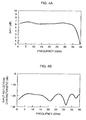
- Fig. 4A is a graphic chart showing a relation between frequency and gain in the second simulation
- Fig. 4B is a graphic chart showing a relation between frequency and input reflection characteristic in the second simulation.
- dotted lines in Fig. 4A and Fig. 4B show results when the voltage Vdio was -2 V
- solid lines show results when the voltage Vdio was 1 V.
- the frequency characteristic of gain is changed by switching the voltage Vdio. Namely, a flatness of the gain becomes good when the voltage Vdio is 1 V than when it is -2 V under the condition of this simulation.
- the voltage Vdio is set to be two kinds, but it may be three kinds or more. Besides, it is preferable to switch all of the switches 12-1 to 12-n simultaneously from a point of view of a simplification of a control, and it is preferable to switch them individually from a point of view of enabling a finer control. This can also be said for the switching of the voltage Vdio.
- Fig. 5 is a circuit diagram showing an oscillator according to the arrangement.
- the arrangement is an arrangement in which a circuit similar to the input capacitance change circuit in the first embodiment is applied to the oscillator as a negative resistance change circuit, though the first embodiment relates to the distributed amplifier.
- a variable capacitance diode 26 and a capacitor 25 are connected in series, and an anode of the variable capacitance diode 26 is grounded.
- a control terminal 21 is connected to a cathode of the variable capacitance diode 26 via a resistor 32.
- a gate of an oscillation transistor 27 is connected to the other end of the capacitor 25.
- An inductor 24 exists between the capacitor 25 and the gate.
- an inductor 23 exists between the capacitor 25 and the ground.
- a capacitor 38 and a resistor 39 are connected to a drain of the oscillation transistor 27, and an output terminal 22 is connected to the other end of the resistor 39. Besides, the other end of the capacitor 38 is grounded.
- An inductor 37 exists between the drain, and the capacitor 38 and the resistor 39.
- an inductor 28 which may be constituted by a ⁇ /4 line exists between the drain and a power voltage supply terminal 33.
- a resistor 29 and a resistor 31 are connected in parallel with each other between a source of the oscillation transistor 27 and the ground.
- a transistor 35 is provided as a switch between the resistor 31 and the source.
- a capacitor 30 and a variable capacitance diode (variable capacitor) 36 are connected in series with each other between the source and the ground.
- a control terminal 34 to which the voltage Vdio is applied when capacitance of the variable capacitance diode 36 is controlled is provided between the capacitor 30 and the variable capacitance diode 36.
- the voltage applied to the control terminal 34 may be selected from plural kinds set in advance.
- a variable resistor circuit may be constituted by the resistor 29, the resistor 31, and the transistor (switch) 35, and a variable capacitor circuit may be constituted by the capacitor 30 and the variable capacitance diode 36. Further, a negative resistance change circuit may be constituted by the variable resistor circuit and the variable capacitor circuit.
- a frequency characteristic is measured after the transistor 35 is turned off and a constant voltage Vdio is applied to the control terminal 34 after it is manufactured. Then, when a desired oscillation frequency is not obtained, the transistor 35 is turned on, or a value of the voltage Vdio applied to the control terminal 34 is switched. As a result, value(s) of the "C s " and/or "R s " between the source of the oscillation transistor 27 and the ground may change, and the negative resistance changes. As a result, the oscillation frequency changes.
- Fig. 6A is a graphic chart showing a relation between frequency, and amount of negative resistance and phase characteristic in the third simulation.
- a dotted line in Fig. 6A shows the amount of the negative resistance (left vertical axis) when the transistor 35 was turned off
- a solid line shows the amount of the negative resistance when the transistor 35 was turned on
- a chain line shows the phase characteristic (right vertical axis) when the transistor 35 was turned off
- a two-dot chain line shows the phase characteristic when the transistor 35 was turned on.
- the amount of the negative resistance changes by switching the on/off of the transistor 35. Namely, the amount of the negative resistance increases when the transistor 35 is turned on than when it is turned off under the condition of this simulation.
- Fig. 6B is a graphic chart showing a relation between frequency, and amount of negative resistance and phase characteristic in the fourth simulation. Incidentally, a dotted line in Fig.
- 6B shows the amount of the negative resistance (left vertical axis) when the voltage Vdio was -2 V
- a solid line shows the amount of the negative resistance when the voltage Vdio was 1 V
- a chain line shows the phase characteristic (right vertical axis) when the voltage Vdio was -2 V
- a two-dot chain line shows the phase characteristic when the voltage Vdio was 1 V.
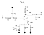
- Fig. 7 is a circuit diagram showing a narrow-band amplifier according to the second arrangement.
- the second arrangement is an arrangement in which a main portion of the first embodiment is applied to the narrow-band amplifier, though the first embodiment relates to the distributed amplifier.
- a capacitor 45 and a gate of an input transistor 47 are connected to an input terminal 41.
- a power supply voltage is supplied to the other end of the capacitor 45.
- an inductor 43 exists between the input terminal 41 and the capacitor 45.
- an inductor 44 exists between the capacitor 45 and the gate.
- a capacitor 58 and an output terminal 42 are connected to a drain of the input transistor 47. Besides, the other end of the capacitor 58 is grounded.
- An inductor 57 exists between the drain, and the capacitor 58 and the output terminal 42.
- an inductor 48 which may be constituted by a ⁇ /4 line exists between the drain and a power voltage supply terminal 53.
- a resistor 49 and a resistor 51 are connected in parallel with each other between a source of the input transistor 47 and the ground.
- a transistor 55 is provided as a switch between the resistor 51 and the source.
- a capacitor 50 and a variable capacitance diode (variable capacitor) 56 are connected in series with each other between the source and the ground.
- a control terminal 54 to which the voltage Vdio is applied when capacitance of the variable capacitance diode 56 is controlled is provided between the capacitor 50 and the variable capacitance diode 56.
- the voltage applied to the control terminal 54 may be selected from plural kinds set in advance.
- a variable resistor circuit may be constituted by the resistor 49, the resistor 51, and the transistor (switch) 55, and a variable capacitor circuit may be constituted by the capacitor 50 and the variable capacitance diode 56.
- An input capacitance change circuit may be constituted by the variable resistor circuit and the variable capacitor circuit.
- a frequency characteristic is measured after, for example, the transistor 55 is turned off and a constant voltage Vdio is applied to the control terminal 54 after it is manufactured. Then, when a desired matching frequency is not obtained, the transistor 55 is turned on or a value the voltage Vdio applied to the control terminal 54 is switched. As a result, value(s) of the C s and/or R s between the source of the input transistor 47 and the ground change, and the matching frequency changes.
- a fifth simulation the simulation is performed under a condition in which the voltage Vdio applied to the control terminal 54 was 1 V, and the on/off of the transistor 55 was switched. Simulation results are shown in Fig. 8A to Fig. 8C .
- Fig. 8A is a graphic chart showing a relation between frequency and gain in the fifth simulation
- Fig. 8B is a graphic chart showing a relation between frequency and input reflection characteristic in the fifth simulation
- Fig. 8C is a graphic chart showing a relation between frequency and output reflection characteristic in the fifth simulation.
- dotted lines in Fig. 8A to Fig. 8C show respective results when the transistor 55 was turned off
- solid lines show respective results when the transistor 55 was turned on.
- a frequency characteristic of the gain changes by switching the on/off of the transistor 55. Besides, there is no bad influence on the input reflection characteristic and the output reflection characteristic as shown in Fig. 8B and Fig. 8C .
- Fig. 9A is a graphic chart showing a relation between frequency and gain in the sixth simulation
- Fig. 9B is a graphic chart showing a relation between frequency and input reflection characteristic in the sixth simulation
- Fig. 9C is a graphic chart showing a relation between the frequency and output reflection characteristic in the sixth simulation.
- dotted lines in Fig. 9A to Fig. 9C show respective results when the voltage Vdio was -1 V
- solid lines show respective results when the voltage Vdio was 1 V.
- a frequency characteristic of the gain changes by switching the voltage Vdio. Besides, there is no bad influence on the input reflection characteristic and the output reflection characteristic as shown in Fig. 9B and Fig. 9C .
- the control of the gain and the adjustment of the matching frequency are possible.
- the matching frequency is easy to vary resulting from the manufacturing environment of the transistor and so on, and therefore, the second arrangement is particularly effective in the case as stated above.
- Fig. 10 is a circuit diagram showing a distributed amplifier according to the second embodiment of the present invention.
- the resistors 9-1 to 9-n are not connected to the sources of the input transistors 7-1 to 7-n, but inductors 17-1 to 17-n which may be constituted by choke coils or 1/4 ⁇ lines are connected thereto.
- a field-effect transistor is used as the transistor, but a bipolar junction transistor may be used instead thereof.
- variable resistor circuit and the variable capacitor circuit for the input capacitance change circuit and the negative resistance change circuit, and an object of the present invention can be attained by providing either one of them.
- the numbers of the switches, resistor elements, variable capacitor elements, and so on provided at the input capacitance change circuit and the negative resistance change circuit are not limited. There is a possibility in which a circuitry, a control, and so on become complicated by using the more numbers of the above, but it becomes possible to perform finer control, adjustment, and so on.
- the configuration of the distributed amplifier is not limited to the one shown in Fig. 1 and so on, but for example, it is possible to apply for a differential amplifier, an amplifier to which plural input transistors are cascaded, and so on.
- semiconductor materials composing these circuits are not limited in particular, and for example, a GaAs series compound semiconductor, an InP series compound semiconductor, a GaN series compound semiconductor, an Si series semiconductor and so on can be used.
- the present invention it is possible to adjust input capacitance of an input transistor by an input capacitance change circuit, and therefore, it is possible to correct a problem even if the problem such as a gain slope occurs after it is manufactured. Besides, in the invention relating to an oscillator, it is possible to adjust an oscillation frequency by adjusting negative resistance.
Landscapes
- Engineering & Computer Science (AREA)
- Power Engineering (AREA)
- Amplifiers (AREA)
- Microwave Amplifiers (AREA)
- Networks Using Active Elements (AREA)
Abstract
Priority Applications (2)
| Application Number | Priority Date | Filing Date | Title |
|---|---|---|---|
| EP10193030.3A EP2296268B1 (en) | 2006-03-20 | 2006-03-20 | Analog circuit |
| EP09179509A EP2166667B1 (en) | 2006-03-20 | 2006-03-20 | Analog circuit |
Applications Claiming Priority (1)
| Application Number | Priority Date | Filing Date | Title |
|---|---|---|---|
| PCT/JP2006/305595 WO2007108103A1 (ja) | 2006-03-20 | 2006-03-20 | アナログ回路 |
Related Child Applications (2)
| Application Number | Title | Priority Date | Filing Date |
|---|---|---|---|
| EP09179509.6 Division-Into | 2009-12-16 | ||
| EP10193030.3 Division-Into | 2010-11-29 |
Publications (3)
| Publication Number | Publication Date |
|---|---|
| EP1998439A1 EP1998439A1 (en) | 2008-12-03 |
| EP1998439A4 EP1998439A4 (en) | 2009-04-15 |
| EP1998439B1 true EP1998439B1 (en) | 2012-02-22 |
Family
ID=38522143
Family Applications (3)
| Application Number | Title | Priority Date | Filing Date |
|---|---|---|---|
| EP10193030.3A Active EP2296268B1 (en) | 2006-03-20 | 2006-03-20 | Analog circuit |
| EP06729563A Active EP1998439B1 (en) | 2006-03-20 | 2006-03-20 | Analog circuit |
| EP09179509A Active EP2166667B1 (en) | 2006-03-20 | 2006-03-20 | Analog circuit |
Family Applications Before (1)
| Application Number | Title | Priority Date | Filing Date |
|---|---|---|---|
| EP10193030.3A Active EP2296268B1 (en) | 2006-03-20 | 2006-03-20 | Analog circuit |
Family Applications After (1)
| Application Number | Title | Priority Date | Filing Date |
|---|---|---|---|
| EP09179509A Active EP2166667B1 (en) | 2006-03-20 | 2006-03-20 | Analog circuit |
Country Status (4)
| Country | Link |
|---|---|
| US (1) | US7782140B2 (ja) |
| EP (3) | EP2296268B1 (ja) |
| JP (1) | JP4952713B2 (ja) |
| WO (1) | WO2007108103A1 (ja) |
Families Citing this family (8)
| Publication number | Priority date | Publication date | Assignee | Title |
|---|---|---|---|---|
| US7973604B2 (en) * | 2007-05-01 | 2011-07-05 | Nxp B.V. | Tunable multi frequency bands filter device |
| FR2935567B1 (fr) * | 2008-08-29 | 2010-09-17 | Thales Sa | Dispositif hyperfrequence large bande a gain commutable |
| JP6579959B2 (ja) * | 2014-02-07 | 2019-09-25 | 株式会社Nbcメッシュテック | 細菌性皮膚病用殺菌組成物 |
| JP2016054452A (ja) | 2014-09-04 | 2016-04-14 | 住友電気工業株式会社 | 光変調器駆動回路 |
| US10622952B2 (en) * | 2018-06-07 | 2020-04-14 | Microsemi Corporation | Distributed amplifier |
| US11515850B2 (en) | 2018-09-04 | 2022-11-29 | Nippon Telegraph And Telephone Corporation | Distributed amplifier |
| JP7263884B2 (ja) * | 2019-03-29 | 2023-04-25 | 日本電信電話株式会社 | 分布型回路 |
| WO2022176117A1 (ja) * | 2021-02-18 | 2022-08-25 | 日本電信電話株式会社 | 電圧制御発振器およびバイアス生成回路 |
Family Cites Families (35)
| Publication number | Priority date | Publication date | Assignee | Title |
|---|---|---|---|---|
| NL236310A (ja) * | 1958-02-19 | |||
| US2957143A (en) * | 1959-09-11 | 1960-10-18 | Arizona Res Foundation | Wideband transistor amplifier |
| NL268847A (ja) * | 1961-08-31 | |||
| US3222611A (en) * | 1962-03-01 | 1965-12-07 | Jr Charles W Norton | Distributed amplifier |
| GB1242213A (en) * | 1967-09-01 | 1971-08-11 | Horace Alexander Johns | Improvements relating to oscillators |
| US3486126A (en) * | 1968-11-15 | 1969-12-23 | Us Army | High performance, wide band, vhf-uhf amplifier |
| FR2435154A1 (fr) * | 1978-09-01 | 1980-03-28 | Labo Electronique Physique | Dispositif de stabilisation en frequence d'un oscillateur hyperfrequence a transistor a effet de champ |
| US4291286A (en) * | 1979-12-17 | 1981-09-22 | Ford Aerospace & Communications Corporation | High bandwidth transversal filter |
| US4498058A (en) * | 1982-05-17 | 1985-02-05 | Sperry Corporation | Low input capacitance amplifier |
| JPS5922416A (ja) * | 1982-07-28 | 1984-02-04 | Fujitsu Ten Ltd | 高周波増幅回路 |
| JPS60190005A (ja) * | 1984-03-12 | 1985-09-27 | Hitachi Ltd | 発振回路 |
| JPS6350204A (ja) * | 1986-08-20 | 1988-03-03 | Alps Electric Co Ltd | 変調回路を備えた高周波発振器 |
| JPH01137705A (ja) * | 1987-11-24 | 1989-05-30 | Sumitomo Electric Ind Ltd | 分布増幅器 |
| JPH01137714A (ja) * | 1987-11-24 | 1989-05-30 | Sumitomo Electric Ind Ltd | ピーキング回路 |
| US4835485A (en) * | 1988-03-25 | 1989-05-30 | General Electric Company | Unconditionally-stable ultra low noise R.F. preamplifier |
| JPH02170602A (ja) * | 1988-12-22 | 1990-07-02 | Sumitomo Electric Ind Ltd | マイクロ波集積回路 |
| FR2644646B1 (fr) * | 1989-03-15 | 1991-05-24 | Alcatel Transmission | Oscillateur hyperfrequence a transistor |
| JP2709509B2 (ja) | 1989-05-15 | 1998-02-04 | 日本電信電話株式会社 | バイポーラトランジスタ増幅回路 |
| US5021743A (en) * | 1989-11-30 | 1991-06-04 | Raytheon Company | Biasing networks for matrix amplifiers |
| JPH04326608A (ja) * | 1991-04-26 | 1992-11-16 | Sumitomo Electric Ind Ltd | 発振回路 |
| US5227734A (en) * | 1991-08-26 | 1993-07-13 | Raytheon Company | Broadband bipolar transistor distributed amplifier |
| JP3111554B2 (ja) * | 1991-11-14 | 2000-11-27 | 日本電気株式会社 | 進行波型増幅回路 |
| JPH05251962A (ja) | 1992-03-09 | 1993-09-28 | Mitsubishi Electric Corp | 増幅器 |
| TW253083B (ja) * | 1993-10-05 | 1995-08-01 | Advanced Micro Devices Inc | |
| JP3056933B2 (ja) | 1993-12-16 | 2000-06-26 | 日本電信電話株式会社 | 分布型バラン |
| JP2881716B2 (ja) * | 1994-03-28 | 1999-04-12 | 株式会社ミリウェイブ | 発振器 |
| JPH08274553A (ja) * | 1995-03-31 | 1996-10-18 | Nippon Telegr & Teleph Corp <Ntt> | 分布増幅器 |
| JPH11261348A (ja) * | 1998-03-10 | 1999-09-24 | Mitsubishi Electric Corp | 電圧増幅器 |
| US6124767A (en) * | 1998-05-21 | 2000-09-26 | Delphi Components, Inc. | RF/Microwave oscillator |
| JP3517780B2 (ja) * | 2000-02-22 | 2004-04-12 | 日本電信電話株式会社 | 能動終端回路およびこれを用いた分布増幅器 |
| JP2001284993A (ja) * | 2000-03-31 | 2001-10-12 | Toshiba Corp | マイクロ波集積回路およびこの製造方法 |
| JP4751002B2 (ja) * | 2001-07-11 | 2011-08-17 | 富士通株式会社 | カスコード型分布増幅器 |
| JP4045959B2 (ja) * | 2003-01-20 | 2008-02-13 | 日本電気株式会社 | 利得可変電圧・電流変換回路とこれを用いたフィルタ回路 |
| US6924697B2 (en) * | 2003-02-27 | 2005-08-02 | Freescale Semiconductor, Inc. | Semiconductor device and method thereof |
| TWI347083B (en) * | 2006-09-26 | 2011-08-11 | Fujitsu Ltd | Conversion circuit for converting differential signal into single-phase signal |
-
2006
- 2006-03-20 EP EP10193030.3A patent/EP2296268B1/en active Active
- 2006-03-20 WO PCT/JP2006/305595 patent/WO2007108103A1/ja not_active Ceased
- 2006-03-20 EP EP06729563A patent/EP1998439B1/en active Active
- 2006-03-20 EP EP09179509A patent/EP2166667B1/en active Active
- 2006-03-20 JP JP2008506111A patent/JP4952713B2/ja active Active
-
2008
- 2008-09-19 US US12/234,105 patent/US7782140B2/en active Active
Also Published As
| Publication number | Publication date |
|---|---|
| WO2007108103A1 (ja) | 2007-09-27 |
| EP1998439A4 (en) | 2009-04-15 |
| EP1998439A1 (en) | 2008-12-03 |
| JPWO2007108103A1 (ja) | 2009-07-30 |
| US20090009253A1 (en) | 2009-01-08 |
| JP4952713B2 (ja) | 2012-06-13 |
| EP2296268A1 (en) | 2011-03-16 |
| EP2166667A2 (en) | 2010-03-24 |
| EP2166667A3 (en) | 2010-05-05 |
| US7782140B2 (en) | 2010-08-24 |
| EP2166667B1 (en) | 2012-02-01 |
| EP2296268B1 (en) | 2013-06-05 |
Similar Documents
| Publication | Publication Date | Title |
|---|---|---|
| US7782140B2 (en) | Analog circuit | |
| JP4121844B2 (ja) | 利得可変型増幅器 | |
| EP2339746B1 (en) | Doherty amplifier with composed transfer characteristic having multiple peak amplifiers | |
| US10263573B2 (en) | Driver with distributed architecture | |
| US8368483B2 (en) | Multiband matching circuit and multiband power amplifier | |
| US6759907B2 (en) | Distributed level-shifting network for cascading broadband amplifiers | |
| JP2002368546A (ja) | 前置歪み補償器とそれを使用する線形増幅器 | |
| JPH09214278A (ja) | Pinダイオード可変減衰器 | |
| JP3574546B2 (ja) | 高周波可変利得増幅器 | |
| JP5161856B2 (ja) | バイアス回路 | |
| KR20120049853A (ko) | 능동 정합을 갖는 분산 전력 증폭기 | |
| JP3886642B2 (ja) | 高周波利得可変増幅回路 | |
| JP2024038377A (ja) | 分布型増幅器 | |
| US7609128B2 (en) | Switch circuit | |
| CN112448677A (zh) | 一种大带宽紧凑型的Doherty 功率放大器结构 | |
| EP2814171B1 (en) | Variable inductor circuit and high frequency circuit | |
| JP3946665B2 (ja) | 大信号高周波スイッチ回路 | |
| JP2012039641A (ja) | アナログ回路 | |
| JP4305618B2 (ja) | 負性抵抗回路、及びアクティブフィルタ | |
| JPH0779132A (ja) | 可変減衰器 | |
| CN117526870A (zh) | 行波放大器的偏置 | |
| JP2004320352A (ja) | 高周波可変減衰器 | |
| JP2001053563A (ja) | マイクロ波増幅器 | |
| KR20060013390A (ko) | 광대역 일정-이득 전압 증폭기 | |
| JPH062827U (ja) | 可変減衰回路素子 |
Legal Events
| Date | Code | Title | Description |
|---|---|---|---|
| PUAI | Public reference made under article 153(3) epc to a published international application that has entered the european phase |
Free format text: ORIGINAL CODE: 0009012 |
|
| 17P | Request for examination filed |
Effective date: 20081015 |
|
| AK | Designated contracting states |
Kind code of ref document: A1 Designated state(s): DE GB |
|
| A4 | Supplementary search report drawn up and despatched |
Effective date: 20090317 |
|
| DAX | Request for extension of the european patent (deleted) | ||
| RBV | Designated contracting states (corrected) |
Designated state(s): DE GB |
|
| 17Q | First examination report despatched |
Effective date: 20090619 |
|
| GRAP | Despatch of communication of intention to grant a patent |
Free format text: ORIGINAL CODE: EPIDOSNIGR1 |
|
| GRAS | Grant fee paid |
Free format text: ORIGINAL CODE: EPIDOSNIGR3 |
|
| GRAA | (expected) grant |
Free format text: ORIGINAL CODE: 0009210 |
|
| AK | Designated contracting states |
Kind code of ref document: B1 Designated state(s): DE GB |
|
| REG | Reference to a national code |
Ref country code: GB Ref legal event code: FG4D |
|
| REG | Reference to a national code |
Ref country code: DE Ref legal event code: R096 Ref document number: 602006027763 Country of ref document: DE Effective date: 20120419 |
|
| PLBE | No opposition filed within time limit |
Free format text: ORIGINAL CODE: 0009261 |
|
| STAA | Information on the status of an ep patent application or granted ep patent |
Free format text: STATUS: NO OPPOSITION FILED WITHIN TIME LIMIT |
|
| 26N | No opposition filed |
Effective date: 20121123 |
|
| REG | Reference to a national code |
Ref country code: DE Ref legal event code: R097 Ref document number: 602006027763 Country of ref document: DE Effective date: 20121123 |
|
| PGFP | Annual fee paid to national office [announced via postgrant information from national office to epo] |
Ref country code: DE Payment date: 20250218 Year of fee payment: 20 |
|
| PGFP | Annual fee paid to national office [announced via postgrant information from national office to epo] |
Ref country code: GB Payment date: 20250220 Year of fee payment: 20 |