EP1964033B1 - Verfahren zur herstellung von rfid-geräten - Google Patents
Verfahren zur herstellung von rfid-geräten Download PDFInfo
- Publication number
- EP1964033B1 EP1964033B1 EP06845409.9A EP06845409A EP1964033B1 EP 1964033 B1 EP1964033 B1 EP 1964033B1 EP 06845409 A EP06845409 A EP 06845409A EP 1964033 B1 EP1964033 B1 EP 1964033B1
- Authority
- EP
- European Patent Office
- Prior art keywords
- interposer
- web
- antenna
- interposers
- cutting
- Prior art date
- Legal status (The legal status is an assumption and is not a legal conclusion. Google has not performed a legal analysis and makes no representation as to the accuracy of the status listed.)
- Active
Links
Images



Classifications
-
- G—PHYSICS
- G06—COMPUTING OR CALCULATING; COUNTING
- G06K—GRAPHICAL DATA READING; PRESENTATION OF DATA; RECORD CARRIERS; HANDLING RECORD CARRIERS
- G06K19/00—Record carriers for use with machines and with at least a part designed to carry digital markings
- G06K19/06—Record carriers for use with machines and with at least a part designed to carry digital markings characterised by the kind of the digital marking, e.g. shape, nature, code
- G06K19/067—Record carriers with conductive marks, printed circuits or semiconductor circuit elements, e.g. credit or identity cards also with resonating or responding marks without active components
- G06K19/07—Record carriers with conductive marks, printed circuits or semiconductor circuit elements, e.g. credit or identity cards also with resonating or responding marks without active components with integrated circuit chips
-
- B—PERFORMING OPERATIONS; TRANSPORTING
- B32—LAYERED PRODUCTS
- B32B—LAYERED PRODUCTS, i.e. PRODUCTS BUILT-UP OF STRATA OF FLAT OR NON-FLAT, e.g. CELLULAR OR HONEYCOMB, FORM
- B32B38/00—Ancillary operations in connection with laminating processes
- B32B38/0004—Cutting, tearing or severing, e.g. bursting; Cutter details
-
- G—PHYSICS
- G06—COMPUTING OR CALCULATING; COUNTING
- G06K—GRAPHICAL DATA READING; PRESENTATION OF DATA; RECORD CARRIERS; HANDLING RECORD CARRIERS
- G06K19/00—Record carriers for use with machines and with at least a part designed to carry digital markings
- G06K19/06—Record carriers for use with machines and with at least a part designed to carry digital markings characterised by the kind of the digital marking, e.g. shape, nature, code
- G06K19/067—Record carriers with conductive marks, printed circuits or semiconductor circuit elements, e.g. credit or identity cards also with resonating or responding marks without active components
- G06K19/07—Record carriers with conductive marks, printed circuits or semiconductor circuit elements, e.g. credit or identity cards also with resonating or responding marks without active components with integrated circuit chips
- G06K19/077—Constructional details, e.g. mounting of circuits in the carrier
- G06K19/07718—Constructional details, e.g. mounting of circuits in the carrier the record carrier being manufactured in a continuous process, e.g. using endless rolls
-
- H—ELECTRICITY
- H10—SEMICONDUCTOR DEVICES; ELECTRIC SOLID-STATE DEVICES NOT OTHERWISE PROVIDED FOR
- H10P—GENERIC PROCESSES OR APPARATUS FOR THE MANUFACTURE OR TREATMENT OF DEVICES COVERED BY CLASS H10
- H10P72/00—Handling or holding of wafers, substrates or devices during manufacture or treatment thereof
- H10P72/70—Handling or holding of wafers, substrates or devices during manufacture or treatment thereof for supporting or gripping
- H10P72/74—Handling or holding of wafers, substrates or devices during manufacture or treatment thereof for supporting or gripping using temporarily an auxiliary support
-
- H—ELECTRICITY
- H10—SEMICONDUCTOR DEVICES; ELECTRIC SOLID-STATE DEVICES NOT OTHERWISE PROVIDED FOR
- H10W—GENERIC PACKAGES, INTERCONNECTIONS, CONNECTORS OR OTHER CONSTRUCTIONAL DETAILS OF DEVICES COVERED BY CLASS H10
- H10W70/00—Package substrates; Interposers; Redistribution layers [RDL]
- H10W70/60—Insulating or insulated package substrates; Interposers; Redistribution layers
- H10W70/611—Insulating or insulated package substrates; Interposers; Redistribution layers for connecting multiple chips together
-
- H—ELECTRICITY
- H10—SEMICONDUCTOR DEVICES; ELECTRIC SOLID-STATE DEVICES NOT OTHERWISE PROVIDED FOR
- H10W—GENERIC PACKAGES, INTERCONNECTIONS, CONNECTORS OR OTHER CONSTRUCTIONAL DETAILS OF DEVICES COVERED BY CLASS H10
- H10W70/00—Package substrates; Interposers; Redistribution layers [RDL]
- H10W70/60—Insulating or insulated package substrates; Interposers; Redistribution layers
- H10W70/699—Insulating or insulated package substrates; Interposers; Redistribution layers for flat cards, e.g. credit cards
-
- B—PERFORMING OPERATIONS; TRANSPORTING
- B32—LAYERED PRODUCTS
- B32B—LAYERED PRODUCTS, i.e. PRODUCTS BUILT-UP OF STRATA OF FLAT OR NON-FLAT, e.g. CELLULAR OR HONEYCOMB, FORM
- B32B2425/00—Cards, e.g. identity cards, credit cards
-
- B—PERFORMING OPERATIONS; TRANSPORTING
- B32—LAYERED PRODUCTS
- B32B—LAYERED PRODUCTS, i.e. PRODUCTS BUILT-UP OF STRATA OF FLAT OR NON-FLAT, e.g. CELLULAR OR HONEYCOMB, FORM
- B32B2519/00—Labels, badges
- B32B2519/02—RFID tags
-
- B—PERFORMING OPERATIONS; TRANSPORTING
- B32—LAYERED PRODUCTS
- B32B—LAYERED PRODUCTS, i.e. PRODUCTS BUILT-UP OF STRATA OF FLAT OR NON-FLAT, e.g. CELLULAR OR HONEYCOMB, FORM
- B32B38/00—Ancillary operations in connection with laminating processes
- B32B38/18—Handling of layers or the laminate
- B32B38/1858—Handling of layers or the laminate using vacuum
-
- Y—GENERAL TAGGING OF NEW TECHNOLOGICAL DEVELOPMENTS; GENERAL TAGGING OF CROSS-SECTIONAL TECHNOLOGIES SPANNING OVER SEVERAL SECTIONS OF THE IPC; TECHNICAL SUBJECTS COVERED BY FORMER USPC CROSS-REFERENCE ART COLLECTIONS [XRACs] AND DIGESTS
- Y10—TECHNICAL SUBJECTS COVERED BY FORMER USPC
- Y10T—TECHNICAL SUBJECTS COVERED BY FORMER US CLASSIFICATION
- Y10T156/00—Adhesive bonding and miscellaneous chemical manufacture
- Y10T156/10—Methods of surface bonding and/or assembly therefor
- Y10T156/1052—Methods of surface bonding and/or assembly therefor with cutting, punching, tearing or severing
- Y10T156/1062—Prior to assembly
-
- Y—GENERAL TAGGING OF NEW TECHNOLOGICAL DEVELOPMENTS; GENERAL TAGGING OF CROSS-SECTIONAL TECHNOLOGIES SPANNING OVER SEVERAL SECTIONS OF THE IPC; TECHNICAL SUBJECTS COVERED BY FORMER USPC CROSS-REFERENCE ART COLLECTIONS [XRACs] AND DIGESTS
- Y10—TECHNICAL SUBJECTS COVERED BY FORMER USPC
- Y10T—TECHNICAL SUBJECTS COVERED BY FORMER US CLASSIFICATION
- Y10T29/00—Metal working
- Y10T29/49—Method of mechanical manufacture
- Y10T29/49002—Electrical device making
- Y10T29/49016—Antenna or wave energy "plumbing" making
-
- Y—GENERAL TAGGING OF NEW TECHNOLOGICAL DEVELOPMENTS; GENERAL TAGGING OF CROSS-SECTIONAL TECHNOLOGIES SPANNING OVER SEVERAL SECTIONS OF THE IPC; TECHNICAL SUBJECTS COVERED BY FORMER USPC CROSS-REFERENCE ART COLLECTIONS [XRACs] AND DIGESTS
- Y10—TECHNICAL SUBJECTS COVERED BY FORMER USPC
- Y10T—TECHNICAL SUBJECTS COVERED BY FORMER US CLASSIFICATION
- Y10T29/00—Metal working
- Y10T29/49—Method of mechanical manufacture
- Y10T29/49002—Electrical device making
- Y10T29/49016—Antenna or wave energy "plumbing" making
- Y10T29/49018—Antenna or wave energy "plumbing" making with other electrical component
-
- Y—GENERAL TAGGING OF NEW TECHNOLOGICAL DEVELOPMENTS; GENERAL TAGGING OF CROSS-SECTIONAL TECHNOLOGIES SPANNING OVER SEVERAL SECTIONS OF THE IPC; TECHNICAL SUBJECTS COVERED BY FORMER USPC CROSS-REFERENCE ART COLLECTIONS [XRACs] AND DIGESTS
- Y10—TECHNICAL SUBJECTS COVERED BY FORMER USPC
- Y10T—TECHNICAL SUBJECTS COVERED BY FORMER US CLASSIFICATION
- Y10T29/00—Metal working
- Y10T29/49—Method of mechanical manufacture
- Y10T29/49002—Electrical device making
- Y10T29/49117—Conductor or circuit manufacturing
- Y10T29/49124—On flat or curved insulated base, e.g., printed circuit, etc.
- Y10T29/4913—Assembling to base an electrical component, e.g., capacitor, etc.
Definitions
- This invention relates to the field of radio frequency identification (RFID) devices, and a method of manufacturing such devices.
- RFID radio frequency identification
- RFID tags and labels have a combination of antennas and analog and/or digital electronics, which may include for example communications electronics, data memory, and control logic. RFID tags and labels are widely used to associate an object with an identification code. For example, RFID tags are used in conjunction with security-locks in cars, for access control to buildings, and for tracking inventory and parcels. Some examples of RFID tags and labels appear in U.S. Pat. Nos. 6,107,920 , 6,206,292 , and 6,262,692 .
- RFID tags and labels include active tags, which include a power source, and passive tags and labels, which do not.
- passive tags in order to retrieve the information from the chip, a "base station” or “reader” sends an excitation signal to the RFID tag or label. The excitation signal energizes the tag or label, and the RFID circuitry transmits the stored information back to the reader. The "reader” receives and decodes the information from the RFID tag.
- RFID tags can retain and transmit enough information to uniquely identify individuals, packages, inventory and the like.
- RFID tags and labels also can be characterized as those to which information is written only once (although the information may be read repeatedly), and those to which information may be written during use. For example, RFID tags may store environmental data (that may be detected by an associated sensor), logistical histories, state data, etc.
- the devices include a transponder comprising a chip having contact pads and at least two coupling elements, which are conductively connected with the contact pads.
- the coupling elements are touch-free relative to each other and formed in a self-supported as well as a free-standing way and are essentially extended parallel to the chip plane.
- the total mounting height of the transponder corresponds essentially to the mounting height of the chip.
- the size and geometry of the coupling elements are adapted for acting as a dipole antenna or in conjunction with an evaluation unit as a plate capacitor.
- the transponders are produced at the wafer level.
- the coupling elements can be contacted with the contact pads of the chip directly at the wafer level, i.e., before the chips are extracted from the grouping given by the wafer.
- Interposers include conductive leads or pads that are electrically coupled to the contact pads of the chips for coupling to the antennas. These pads provide a larger effective electrical contact area than ICs precisely aligned for direct placement without an interposer. The larger area reduces the accuracy required for placement of ICs during manufacture while still providing effective electrical connection. IC placement and mounting are serious limitations for high-speed manufacture.
- the prior art discloses a variety of RFID strap or interposer structures, typically using a flexible substrate that carries the interposer's contact pads or leads.
- Another type of prior art RFID inlet manufacture using interposers is based on a technique for manufacturing microelectronic elements as small electronic blocks, associated with Alien Technology Corporation ("Alien") of Morgan Hill California.
- Alien has developed techniques to manufacture small electronic blocks, which it calls “NanoBlocks", and then deposit the small electronic blocks into recesses on an underlying substrate.
- a planar substrate is embossed with numerous receptor wells 210.
- the receptor wells are typically formed in a pattern on the substrate.
- the receptor wells 210 may form a simple matrix pattern that may extend over only a predefined portion of the substrate, or may extend across substantially the entire width and length of the substrate, as desired.
- Alien has a number of patents on its technique, including U.S.
- interposers are severed or separated from a webstock or sheetstock with densely packed IC's (i.e. small pitch between adjacent ICs) and interposer leads.
- the interposers are then transported, "indexed” (spread apart), and affixed in sequence to a webstock containing antennas that are typically spaced at a much higher pitch.
- a method of forming RFID devices comprising: iteratively performing the following steps for multiple iterations: feeding a free end of an interposer web consisting of a plurality of interposers into a cutter, wherein the interposer web includes an interposer substrate and each of the interposers includes a section of said substrate, upon which are located conductive leads and an RFID transponder chip, wherein the feeding includes moving the free end with a non-constant speed; butt cutting an interposer from the free end of the interposer web onto a rotary transport mechanism without leaving any matrix material of the interposer web behind on the interposer web; transporting the interposer on the rotary transport mechanism; transferring the interposer from the rotary transport mechanism to a moving antenna web; and attaching the interposer to the antenna web, such that the interposer is operatively coupled to an antenna of the antenna web, wherein the butt cutting includes using a rotary cutter to butt cut the interposer onto an an
- Fig. 1 is a schematic view of an RFID device fabrication system in accordance with the present invention
- Fig. 2 is a high-level flowchart showing some steps of a method for making RFID devices, using a system such as that shown in Fig. 1 , in accordance with the present invention
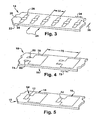
- Fig. 3 is an oblique view showing a portion of the interposer web of Fig. 1 ;
- Fig. 4 is an oblique view showing a portion of the antenna web of Fig. 1 ;
- Fig. 5 is an oblique view showing a portion of a web of RFID devices made using the system of Fig. 1 , and by the method of Fig. 2 ;
- Fig. 6 is a side schematic view showing a first step in a cutting and attaching process using the system of Fig. 1 ;
- Fig. 7 is a side schematic view showing a second step in a cutting and attaching process using the system of Fig. 1 ;
- Fig. 8 is a side schematic view showing a third step in a cutting and attaching process using the system of Fig. 1 ;
- Fig. 9 is a side schematic view showing a fourth step in a cutting and attaching process using the system of Fig. 1 ;
- Fig. 10 is a side schematic view showing a fifth step in a cutting and attaching process using the system of Fig. 1 ;
- Fig. 11 is a side schematic view showing a first step in another cutting and attaching process using the system of Fig. 1 ;
- Fig. 12 is a side schematic view showing a second step in the another cutting and attaching process using the system of Fig. 1 ;
- Fig. 13 is a side schematic view showing a third step in the another cutting and attaching process using the system of Fig. 1 ;
- Fig. 14 is a side view of an alternate pressured belt device usable with the system of Fig. 1 .
- a method of making RFID devices includes feeding in an interposer web or sheet at a variable (non-constant) speed, cutting single interposers from the interposer web or sheet, and using a rotary transport device to transport the singulated (cut) interposers to an antenna web.
- the interposers are transferred from the rotary transport device and are attached to the antenna web, being operatively coupled to antennas on the antenna web.
- the interposers each include an RFID transponder chip and conductive leads.
- the rotary transport device may be a vacuum anvil that acts as an anvil to aid cutting of the interposers from the interposer web, and uses suction to keep the interposers coupled to the rotary transport device.
- a feeder is used to advance the interposer web or sheet into a cutting zone between the rotary cutter and the rotary transport device.
- the rotary cutting device is capable of singulating multiple interposers at one time, and the system is capable of thus being able to remove interposers that are not to be joined to the antenna web, for instance interposers that have failed testing, thereby removing these unwanted interposers.
- Fig. 1 shows a fabrication system 10 for fabricating RFID devices
- Fig. 2 shows some steps of a method 100 that uses the fabrication system 10 in order to make RFID devices.
- the general goal of the system 10 and the method 100 is to cut or otherwise singulate interposers 12 of an interposer web 14, and attach the interposers 12 to operatively couple the interposers 12 to antennas 16 on an antenna web 18.
- RFID devices 20 are produced, with each of the devices 20 including an interposer 12 coupled to an antenna 16.
- Fig. 3 illustrates one example of the interposer web 14 consisting of a plurality of the interposers 12.
- the interposer web 14 includes an interposer substrate 22.
- Each of the interposers 12 includes a substrate section 24 of the substrate 22, upon which are located conductive leads 26 and an RFID transponder chip 28.
- interposer includes an integrated circuit (IC) chip, electrical connectors to the chip, and interposer leads coupled to the electrical connectors.
- An interposer also includes an interposer substrate, as described above, which may support other elements of the interposer, and may provide other characteristics such as electrical insulation.
- the interposer may be elongate, as the interposer leads extend from the IC chip.
- the interposer may be flexible, rigid, or semi-rigid. It will be appreciated that a variety of interposer configurations are available for coupling to antennas. Examples include an RFID interposer available from Alien Technology Corporation, and the interposer marketed under the name I-CONNECT, available from Philips Electronics. Further disclosures of interposers are found in U.S. Patent No. 6,606,247 , assigned to Alien Technology Corporation, and in U.S. Patent Publication No. 2003/0136503 A1 .
- the interposer substrate 22 may be any of a variety of suitable materials.
- suitable materials include high Tg polycarbonate, poly(ethylene terephthalate), polyarylate, polysulfone, a norbornene copolymer, poly phenylsulfone, polyetherimide, polyethylenenaphthalate (PEN), polyethersulfone (PES), polycarbonate (PC), a phenolic resin, polyester, polyimide, polyetherester, polyetheramide, cellulose acetate, aliphatic polyurethanes, polyacrylonitrile, polytrifluoroethylenes, polyvinylidene fluorides, HOPEs, poly(methyl methacrylates), or a cyclic or acyclic polyolefin.
- suitable polymer materials may be utilized for the interposer substrate 22.
- suitable non-polymer materials, such as paper may also be used for the interposer substrate 22.
- interposer web 14 is shown as a roll material, being unwound from an interposer web supply roll 30. It will be appreciated that the interposer web 14 alternatively may be a suitable interposer sheet material, being provided in a plurality of distinct sheets.
- the interposer web 14 illustrated in Fig. 3 is shown having a single lane of the interposers 12, located adjacent to one another at an interposer pitch 32 in a downweb direction 34.
- the "pitch" of elements on a webstock or sheetstock means the center-to-center distance between adjacent elements.
- a lower pitch (less distance between adjacent elements) is sometimes referred to as a higher density pitch, and vice versa.
- the interposer web 14 may have multiple lanes of interposers in a crossweb direction 36. Suitable splitting operations may be utilized, if desired, to separate a multi-lane into single lanes, prior to cutting or otherwise singulating the interposers 12.
- a feeder 40 is used to advance the interposer web 14, for instance moving the web by rotation of feeder rollers 42, which press upon and grip the interposer web 14.
- step 102 of the method 100 a determination is made regarding the amount of a free end 44 of the interposer web 14 that is to be advanced for the next cut.
- the system 10 may be configured to cut multiple of the interposers 12 when a single cut is made on the interposer web 14. This may allow for interposers that have failed testing or otherwise not to be used, to be removed and discarded during the cutting process.
- Information regarding the location of unusable of the interposers 12 may be used to control the feeder 40 to advance an extra amount of the interposer web 14, when required to allow removal of unusable of the interposers 12.
- step 104 of the method 100 the feed rollers 42 or other components of the feeder 40 are used to advance the desired amount of the free end 44 of the interposer web 14.
- This advancement of the interposer web 14 is made at a variable, non-constant speed.
- the rotation of the feeder rollers 42 may speed up and slow down to feed different amounts of the interposer web 14, and/or as part of the cyclic process of feeding the interposer web 14.
- one of the interposers 12 is singulated from the interposer web 14 at a cutter/transporter 46.
- the cutter/transporter includes a rotary cutter 48, a rotary transporter 50, and a roller 52.
- the free end 44 of the interposer web 14 is cut between the rotary cutter 48 and an anvil that is part of the rotary transporter 50.
- the cutting is butt cutting of the interposer web 14, singulating one of the interposers 12 from the free end 44 of the interposer web 14, without leaving any matrix of the material behind on the interposer web 14. It will be appreciated that use of butt cutting advantageously avoids having to deal with any remaining matrix material of the interposer web 14.
- a suction chute 58 is positioned in proximity to a cutting region 60.
- the suction chute 58 is used to receive and remove additional material that is cut from the interposer web 14. The removal of this additional material may occur in step 110 of the method 100.
- the additional material consists of include additional interposers that are not to be attached to the antenna web 18, for instance additional interposers that have been already identified as unsuitable for use, such as by failing earlier-performed testing.
- the feeder 40 may retract the interposer web 14, in step 112.
- the interposer web 14 may overshoot the cutting region 60 for inertial reasons, and may need to be retracted by the feeder 40 prior to the next cutting operation.
- the singulated interposer 12 is transported on the rotary transporter 50 from the cutting region 60 to an attachment region 64.
- the rotary transporter 50 may be a vacuum anvil device that includes locations that serve as an anvil during the cutting operation performed in the cutting region 60. Vacuum ports may also be located at the same locations along the rotary transporter 50, enabling the singulated interposers 12 to be sucked toward and held against the rotary transporter 50. As the rotary transporter 50 turns, the singulated interposers 12 are moved along to the attachment region 64, where the interposers 12 are attached to individual antenna 16 of the antenna web 18.
- Fig. 4 shows one example of the layout of the antenna web 18, with multiple antennas 16 spaced at an antenna pitch 70 in a downweb direction 72.
- the antenna web 18 includes an antenna web substrate 74 upon which conductive antenna patterns 78 of the antennas 16 rest.
- the conductive antenna patterns 78 may be made by any of a variety of suitable processes for forming conductive patterns.
- the antenna conductive patterns may be made from, for example, copper, silver, aluminum or other thin conductive material (such as etched or hot-stamped metal foil, printed conductive ink, etched metal, sputtered metal, etc.). It will be appreciated that a wide variety of suitable antenna patterns are known.
- each of the antennas 16 may include one or more adhesive pads 80 for securing the singulated interposers 12 to the antenna web 18.
- the adhesive pads 80 may include any of a variety of conductive or non-conductive adhesives.
- the adhesive pads 80 may include pressure sensitive adhesives, conductive epoxy adhesives, and/or heat-curable adhesives. A wide variety of permanent pressure sensitive adhesives and heat-curable adhesives are well known in the art.
- the pressure sensitive adhesive may be one of any number of different types of adhesives, such as acrylic and elastomeric pressure sensitive adhesives.
- the antenna web substrate 74 may include any of a variety of suitable substrate materials, such as the materials mentioned above with regard to the interposer web substrate 22.
- the antenna web 18 may be a roll material, which may be supplied in an antenna web supply roll 84.
- the antenna web 18 may be moved at a substantially constant velocity to a take-up roll 86.
- the singulated interposers 12 held by the transporter 50 may be released onto the antenna web at suitable positions relative to the antenna 16, in step 116.
- the release may be caused by the interposer 12 adhering to the adhesive pads 80 on the antenna web substrate 18.
- other methods may be used to release the singulated interposers 12 from the rotary transporter 50 to the antenna web 18. For instance a release of the vacuum suction holding the singulated interposer 12 to the rotary transporter 50 may be utilized to release the interposer 12.
- step 120 there may be a need to cure the adhesive in step 120, at a curing station 90 of the system 10.
- suitable heating may be provided at the curing station 90.
- the completed web of RFID devices 94 may be wound up in the take-up roll 86.
- Fig. 5 shows the RFID devices 94, with the singulated interposers 12 attached to and operatively coupled to the antennas 16.
- the interposers 12 may be coupled in a face-down configuration with the conductive leads 26 towards and/or in contact with the conductive antenna pattern 78.
- the interposers 12 may be coupled in a face-up configuration, with interposer substrate sections 24 between the conductive leads 26 and the conductive antenna pattern 78. It will be appreciated that various types of electrical coupling may be provided between the conductive leads 26 of the interposer 12, and the antenna conductive patterns 78 of the antennas 16.
- Various mechanisms may be used to make a direct electrically or ohmically conductive connection between the interposer conductive leads 26 and the antenna conductive patterns 78.
- other sorts of electrical couplings such as capacitive coupling and/or magnetic coupling, may be used to operatively electrically couple the interposer conductive leads 26 and the antenna conductive patterns 78.
- the antenna may be coated on a plastic film such as Mylar, having a thickness of approximately 2-5 mil.
- the thickness of this particular label embodiment, including a release-coated backing sheet, is between approximately 15-20 mils.
- the web of the RFID devices 94 may be processed further, as appropriate, to add layers or other features to make RFID labels and/or tags.
- additional adhesive layers may be added, additional protective or writable coatings or layers may be added, etc.
- Additional processing steps may be performed as part of the same roll-to-roll operation that includes coupling of the interposers 12 to the antennas 16.
- the additional operations may be performed in one or more different processes. Included in such processes may be separation of the individual RFID devices from a web of such devices, and ultimate coupling of RFID devices to suitable objects.
- Figs. 6-10 schematically illustrate, in greater detail, steps in the singulating of an interposer 12 from the interposer web 14, and transporting and attaching the interposer 12 to the antenna web 18.
- Fig. 6 shows the free end 44 of the interposer web 14 approaching the cutting region 50.
- the interposer web 14 is advanced by the feeder rollers 42 of the feeder 40.
- the rotary cutter 48 is turning, bringing one of the cutting blade sets 200 into position to singulate one of the interposers 12 from the interposer web 14.
- the rotary cutter 48 has two cutting blade sets 200, each including a leading cutting blade 202 and a trailing cutting blade 204.
- the two cutting blade sets 200 are diametrically opposed from one another. It will be appreciated that the rotary cutter 48 may alternatively have a different number of cutting blade sets 200. It would be expected that the cutting blade sets 200 would be circumferentially evenly spaced about the rotary cutter 48.
- Fig. 7 illustrates the actual cutting operation to singulate the interposer 12 from the free end 44 of the interposer web 14.
- the trailing blade 204 of the cutting blade set 200 makes contact with the interposer web 14 as the interposer web 14 is pressed against an anvil 210 of the rotary transporter 50.
- the anvil 210 is positioned around a vacuum nozzle 212 through which a vacuum is maintained in order to releasably secure the cut interposer 12 to the rotary transporter 50.
- the anvil 210 and the vacuum nozzle 212 constitute a receiving station 214 for receiving and transporting the singulated interposers 12.
- the actual cutting of the interposer 12, which is butt cutting the interposer 12, is performed by the trailing cutting blade 204.
- the leading cutting blade 202 may be used for removing additional unusable interposers and/or additional material from the interposer web 14, as part of the same cutting operation.
- the free end 44 of the interposer 14 is held against the anvil 210 by the suction provided through the vacuum nozzle 212. Once the interposer 12 is cut or otherwise singulated, the suction through the vacuum nozzle 212 holds the singulated interposer 12 against the rotary transporter 50.
- Fig. 8 illustrates movement of the singulated interposer 12 on the rotary transporter 50.
- the rotary transporter rotates in a direction opposite to that of the rotary cutter 48 and the roller 52.
- the rotary transporter 50 and the roller 52 may act in concert to advance along the antenna web 18.
- All of the rotary elements of the cutter/transporter 46 (the rotary cutter 48, the rotary transporter 50, and the roller 52) may rotate at substantially constant rates. Alternatively, it will be appreciated that the rotation rates of one or more of the elements may be non-constant. For instance, the rotary transporter 50 may accelerate and decelerate throughout its rotation.
- the rotary transporter 50 may be configured to be substantially stationary during the cutting operation to singulate one of the interposers 12, and may accelerate to move at approximately the speed of the antenna web 18 when the interposer 12 is deposited onto the antenna web 18. It will be appreciated that such a non-constant rotation of the rotary transporter 50 may require that none of the stations 214 for receiving and transporting the interposers 12 (consisting of the anvil 210 and suction nozzle 212) are diametrically opposed to other stations 214. Thus there may be an odd number of circumferentially distributed stations 214 about the circumference of the rotary transporter 50. More broadly, it will be appreciated that the sizes, configurations, and rotation rates of the rotary cutter 48, the rotary transporter 50, and the roller 52, may all be suitably selected to attach the interposers 12 at the proper pitch of the antenna web 18.
- the free end 44 of the interposer web 14 may overshoot the cutting region 60 after the cutting operation has been performed. This overshoot may occur because of inertial forces in accelerating the interposer web 14 to advance it into the cutting region 60 for cutting by the trailing cutting blade 204. It may be desirable to have the interposer web 14 moving during the cutting operation, for example to substantially match the speed of the rotary cutter 48 and/or the speed of the rotary transporter 50. The overshoot may be taken up by retracting the interposer web 14, such as by reversing directions on the feeder rollers 42 of the feeder 40, as is illustrated in Fig. 8 . Thus it may be desirable to advance and retract the interposer web 14 cyclically during the cutting and transporting operation.
- Fig. 9 shows the interposer web 14 retracted and ready to be advanced again for another cutting operation on the free end 44. Meanwhile, the singulated interposer 12 is advancing toward the attachment region 64.
- Fig. 10 shows attachment of the singulated interposer 12 onto the antenna web 18.
- the attachment may include an adhesive attachment of the interposer 12 onto the antenna web 18.
- the vacuum suction on the vacuum nozzle 212 may be reduced or released to aid in releasing the singulated interposer 12 from the rotary transporter 50.
- the rotary transporter 50 may be configured such that the vacuum in the vacuum nozzle is reduced or eliminated automatically as the transporter 50 rotates to bring the singulated interposer in contact with the antenna web 18.
- Figs. 11-13 illustrate an embodiment of the process of the present invention, where multiple portions of the interposer web 14 are cut in a single cutting operation.
- Fig. 11 shows the free end 44 of the interposer web 14 advancing into the cutting region 60 between the rotary cutter 48 and the rotary transporter 50.
- the suction chute 58 is positioned at a far side of the cutting region 60.
- Fig. 12 illustrates the cutting. Both of the cutting blades 202 and 204 of the cutting set 200 butt cut the free end 44 of the interposer web 14, against the anvil 210 of the rotary transporter 50. One cut portion of the interposer web 14 is the singulated interposer 12 between the two cutting blades 202 and 204. The singulated interposer 12 is releasably secured to the rotary transporter 50 by use of the vacuum nozzle 212, in a similar manner to the method shown in Figs. 6-10 and described above.
- An additional cut portion 220 of the interposer web 14 is beyond the front cutting blade 202, at the free end 44 of the interposer web 14.
- This additional portion 220 is a portion of the interposer web 14 to be discarded.
- the additional portion 220 includes one or more interposers that are not to be attached to the antenna web 18.
- the additional portion 220 may include one or more interposers that have failed testing, and thus are to be discarded.
- Fig. 13 illustrates the immediate aftermath of the cutting operation.
- the singulated interposer 12 is secured to the rotary transporter 50, and is being transported toward the antenna web 18.
- the joining of the singulated interposer 12 to the antenna web 18 may follow thereafter along the lines described above with regard to Figs. 9 and 10 .
- the additional portion 220 is directed into the suction chute 58 and is transported out of the cutting region 60, to be eventually discarded. It will be appreciated that a suitable vacuum source may be used to provide suction for operating the suction chute 58, and to pull the additional portions 220 into the suction chute, and to a location to be eventually discarded.
- the systems and methods described herein allow for connection of interposers having a first pitch to antennas on an antenna web having a second pitch.
- the feeder 40 may also be used to adjust the amount of advancement of the interposer web 14 to account for variable pitch among the interposers 12 of the interposer web 14, and/or to account for unusable interposers on the interposer web 14. It will be appreciated that information regarding the location of good interposers on the interposer web 14 may be supplied to the feeder 40 by any of a variety of suitable methods.
- the feeder 40 may be directly coupled to a test device that examines or tests the interposers 12, with the information on the test results being used to suitably advance the interposer web 14 for butt cutting and use of the next available good interposer 12 on the interposer web 14. Also information on positioning of the interposers 12 on the interposer web 14 may be supplied to the feeder 40. Such information may be obtained by various suitable devices, such as optical scanners that locate the position of the interposers 12 and/or index marks indicating the position of interposers on the interposer web 14. Information regarding the interposers may be provided directly to the feeders 40, or may be provided in the form of various types of suitable computer-readable media.
- Fig. 14 shows an alternative pressure lamination member 250 that may be substituted in place of the roller 52.
- the pressure lamination member 250 which may be a metal or polymeric belt, may be used for bonding the interposers 12 on the rotary transporter 50 to the antennas 16 on the antenna web 18.
- the use of a rotating pressure lamination member 250 provides an extended zone of elevated pressure and/or temperature to facilitate adhesive curing, and formation of a durable, bond between the antenna 16 and the interposer 12.
- One or more additional set of belt or roller combinations can be provided to further extend the zone of bond formation between the antenna 16 and the interposer 12.
Landscapes
- Engineering & Computer Science (AREA)
- Computer Hardware Design (AREA)
- Microelectronics & Electronic Packaging (AREA)
- Physics & Mathematics (AREA)
- General Physics & Mathematics (AREA)
- Theoretical Computer Science (AREA)
- Credit Cards Or The Like (AREA)
- Details Of Aerials (AREA)
Claims (6)
- Verfahren zur Herstellung von RFID-Vorrichtungen (20, 94), wobei das Verfahren umfaßt: iteratives Durchführen der folgenden Schritte für mehrfache Iterationen: Zuführen eines freien Endes einer Interposer-Bahn (14), bestehend aus einer Vielzahl von Interposern (12), in eine Schneidvorrichtung, wobei die Interposerbahn (14) ein Interposersubstrat (22) einschließt und jeder der Interposer (12) einen Abschnitt (24) des Interposer-Substrats (22) einschließt, worauf leitfähige Leitungen (26) und ein RFID-Transponderchip (28) angeordnet sind, Endteil-Abschneiden eines Interposer (12) von dem freien Ende (44) der Interposerbahn (14) auf einem rotierenden Transportmechanismus ohne Zurücklassen jedweden Matrixmaterials der Interposerbahn (14) auf der Interposerbahn (14), Transportieren des Interposer auf dem rotierenden Transportmechanismus (50), Übertragen des Interposer von dem rotierenden Transportmechanismus zu einer sich bewegenden Antennenbahn (18) und Anbringen des Interposer an die Antennenbahn (18) derart, daß der Interposer betriebsfähig an eine Antenne (16) der Antennenbahn (18) gekoppelt wird, wobei das Endteil-Abschneiden das Verwenden einer rotierenden Schneidvorrichtung (48) einschließt, um den Interposer auf einem Mutterstück des rotierenden Transportmechanismus abzuschneiden, und wobei die rotierende Schneidvorrichtung (48) Mehrfachblätter (200) einschließt, konfiguriert zum Kontaktieren verschiedener Stellen auf dem freien Ende (44) der Interposerbahn (14) in einer einzelnen Schneidoperation, dadurch gekennzeichnet, daß das Zuführen das Bewegen des freien Endes (44) mit einer nicht konstanten Geschwindigkeit einschließt, weiter gekennzeichnet dadurch daß das Endteil-Abschneiden das Verwenden der Mehrfachblätter (200) einschließt, um einen zusätzlichen Interposer abzuschneiden, der nicht an die Antennenbahn entlang mit dem Interposer verbunden ist, wobei der Interposer und der zusätzliche Interposer, der nicht an die Antennenbahn zu verbinden ist, im wesentlichen gleichzeitig in der einzelnen Schneidoperation abgeschnitten werden, und weiter gekennzeichnet durch das Entfernen der zusätzlichen Interposer, die nicht an die Antennenbahn zu verbinden sind, wobei das Entfernen das Verwenden von Saugzug einschließt, um den zusätzlichen Interposer, der nicht an die Antennenbahn zu verbinden ist, von der Schneidvorrichtung wegzuziehen, und wobei die Verwendung von Saugzug das Saugen des zusätzlichen Interposer in eine Rinne bzw. Rutsche einschließt.
- Verfahren gemäß Anspruch 1, wobei das Zuführen das Fortschreiten bzw. Vorrücken der Interposerbahn (14) mit einem Zulieferer (40) einschließt und wobei der Zulieferer (40) auch die Interposerbahn (14) nach dem Endteil-Abschneiden zurückzieht.
- Verfahren nach Anspruch 1, wobei das Zuführen verschiedene Mengen des freien Endes (44) in verschiedenen Iterationen einschließt.
- Verfahren gemäß Anspruch 1, wobei das Zuführen das Beschleunigen und Abbremsen der Rotation der Zuliefererwalzen (42) einschließt.
- Verfahren gemäß Anspruch 1, wobei das Zuführen das Verwenden eines Zulieferers mit variabler Geschwindigkeit einschließt, um das freie Ende (44) in einen Schneidbereich (60) zuzuführen.
- Verfahren gemäß einem der Ansprüche 1 bis 5, wobei die Interposerbahn (14) einen Interposer-Pitch (32) in einer Richtung bahnabwärts (34) aufweist, der von höherer Dichte als ein Antennen-Pitch (70) in einer Richtung bahnabwärts (72) der Antennenbahn (18) ist.
Applications Claiming Priority (2)
| Application Number | Priority Date | Filing Date | Title |
|---|---|---|---|
| US11/315,504 US7555826B2 (en) | 2005-12-22 | 2005-12-22 | Method of manufacturing RFID devices |
| PCT/US2006/047697 WO2007078823A2 (en) | 2005-12-22 | 2006-12-14 | Method of manufacturing rfid devices |
Publications (2)
| Publication Number | Publication Date |
|---|---|
| EP1964033A2 EP1964033A2 (de) | 2008-09-03 |
| EP1964033B1 true EP1964033B1 (de) | 2013-10-23 |
Family
ID=38123796
Family Applications (1)
| Application Number | Title | Priority Date | Filing Date |
|---|---|---|---|
| EP06845409.9A Active EP1964033B1 (de) | 2005-12-22 | 2006-12-14 | Verfahren zur herstellung von rfid-geräten |
Country Status (4)
| Country | Link |
|---|---|
| US (2) | US7555826B2 (de) |
| EP (1) | EP1964033B1 (de) |
| CN (1) | CN101341501B (de) |
| WO (1) | WO2007078823A2 (de) |
Families Citing this family (40)
| Publication number | Priority date | Publication date | Assignee | Title |
|---|---|---|---|---|
| DE102006007423A1 (de) * | 2005-11-17 | 2007-05-31 | Mühlbauer Ag | Vorrichtung und Verfahren zum Testen der Lesezuverlässigkeit von Smart Labels |
| US20070146135A1 (en) * | 2005-12-27 | 2007-06-28 | David Boyadjieff | Assembling RFID components using webs |
| US8786510B2 (en) | 2006-01-24 | 2014-07-22 | Avery Dennison Corporation | Radio frequency (RF) antenna containing element and methods of making the same |
| JP4952280B2 (ja) * | 2007-02-09 | 2012-06-13 | 富士通株式会社 | 電子装置製造システムおよび電子装置製造方法 |
| JP4952927B2 (ja) * | 2007-08-02 | 2012-06-13 | ブラザー工業株式会社 | 無線タグ作成装置 |
| US10262167B2 (en) | 2008-01-31 | 2019-04-16 | Smartrac Technology Fletcher, Inc. | Detachable radio frequency identification switch tag |
| US10339436B2 (en) | 2015-05-21 | 2019-07-02 | Smartrac Technology Fletcher, Inc. | Multi-frequency radio frequency identification tag |
| US20100301005A1 (en) * | 2009-05-29 | 2010-12-02 | Nilsson Peter L J | Method of Manufacturing an Electrical Circuit on a Substrate |
| US20100301006A1 (en) * | 2009-05-29 | 2010-12-02 | Nilsson Peter L J | Method of Manufacturing an Electrical Component on a Substrate |
| US8267494B2 (en) * | 2009-12-09 | 2012-09-18 | Hand Held Products, Inc. | Automatic RFID circuit tuning |
| US8763898B2 (en) * | 2010-03-02 | 2014-07-01 | First Data Corporation | Advanced card merge machine |
| JP5672067B2 (ja) * | 2010-03-09 | 2015-02-18 | 株式会社リコー | 可逆性感熱記録媒体の製造方法及び製造装置、並びに可逆性感熱記録媒体 |
| EP2580715B1 (de) | 2010-06-14 | 2019-05-22 | Avery Dennison Corporation | Verfahren, system und vorrichtung zur herstellung von kurzfristigen rfid etiketten |
| US9412061B2 (en) * | 2010-08-13 | 2016-08-09 | Avery Dennison Corporation | Sensing radio frequency identification device with reactive strap attachment |
| US10102685B2 (en) | 2011-05-06 | 2018-10-16 | Neology, Inc. | Self declaring device for a vehicle using restrict traffic lanes |
| EP2710524B1 (de) * | 2011-05-06 | 2019-01-23 | Neology, Inc. | Rfid-wechseletikett |
| US11948035B2 (en) | 2011-05-06 | 2024-04-02 | Neology, Inc. | RFID switch tag |
| US10885418B2 (en) | 2011-05-06 | 2021-01-05 | Neology, Inc. | Detachable radio frequency identification switch tag |
| BR112014000269A2 (pt) | 2011-07-05 | 2017-02-14 | Avery Dennison Corp | adesivo resistente à lavagem para rótulos de bebida |
| US9579253B2 (en) * | 2012-11-08 | 2017-02-28 | Grifols Worldwide Operations Limited | RFID tag and blood container/system with integrated RFID tag |
| US9252478B2 (en) | 2013-03-15 | 2016-02-02 | A.K. Stamping Company, Inc. | Method of manufacturing stamped antenna |
| CN104377439B (zh) | 2013-08-15 | 2019-08-27 | 德昌电机(深圳)有限公司 | 天线电路及制造方法 |
| US9424507B2 (en) | 2014-04-01 | 2016-08-23 | Nxp B.V. | Dual interface IC card components and method for manufacturing the dual-interface IC card components |
| US10839279B2 (en) * | 2015-03-31 | 2020-11-17 | Vorbeck Materials Corp. | Transponder fabrication methods |
| EP3079105B1 (de) * | 2015-04-08 | 2021-03-31 | Nxp B.V. | Chipkarte mit doppelschnittstellenkomponenten und verfahren zur herstellung der chipkarte mit doppelschnittstellenkomponenten |
| US11403506B2 (en) | 2015-05-21 | 2022-08-02 | Neology, Inc. | Detachable radio frequency identification switch tag |
| CN105070674B (zh) * | 2015-07-31 | 2018-01-09 | 华中科技大学 | 一种适用于成卷柔性电子器件的逐片转移装置 |
| CA3000311C (en) | 2015-10-01 | 2019-01-08 | Star Systems International, Ltd. | Switchable radio-frequency identification tag device |
| SE542007C2 (en) * | 2017-10-13 | 2020-02-11 | Stora Enso Oyj | A method and an apparatus for producing a radio-frequency identification transponder |
| WO2019224575A1 (en) | 2018-05-22 | 2019-11-28 | Tyco Fire & Security Gmbh | Elongate flexible tag |
| TWI684135B (zh) * | 2018-07-17 | 2020-02-01 | 昱盛國際企業股份有限公司 | 智能膠帶及使用其的物流系統 |
| US12223814B2 (en) | 2019-09-16 | 2025-02-11 | Sensormatic Electronics, LLC | Security tag for textiles using conductive thread |
| US11443160B2 (en) | 2019-09-18 | 2022-09-13 | Sensormatic Electronics, LLC | Systems and methods for laser tuning and attaching RFID tags to products |
| US10970613B1 (en) | 2019-09-18 | 2021-04-06 | Sensormatic Electronics, LLC | Systems and methods for providing tags adapted to be incorporated with or in items |
| US11055588B2 (en) | 2019-11-27 | 2021-07-06 | Sensormatic Electronics, LLC | Flexible water-resistant sensor tag |
| US12524640B2 (en) | 2019-11-27 | 2026-01-13 | Sensormatic Electronics, LLC | Flexible water-resistant sensor tag |
| US11755874B2 (en) | 2021-03-03 | 2023-09-12 | Sensormatic Electronics, LLC | Methods and systems for heat applied sensor tag |
| US20230116340A1 (en) * | 2021-10-08 | 2023-04-13 | Wits Co., Ltd. | Method of manufacturing wireless charging coil module coated with magnetic material on surface of coil |
| US11869324B2 (en) | 2021-12-23 | 2024-01-09 | Sensormatic Electronics, LLC | Securing a security tag into an article |
| IT202200003290A1 (it) * | 2022-02-22 | 2023-08-22 | Pearfid Soc A Responsabilita Limitata Semplificata | Metodo di realizzazione di dispositivi a radiofrequenza |
Family Cites Families (207)
| Publication number | Priority date | Publication date | Assignee | Title |
|---|---|---|---|---|
| US3724737A (en) * | 1971-10-06 | 1973-04-03 | E Bodnar | Spreader for slit web material |
| US3891157A (en) * | 1973-06-04 | 1975-06-24 | Beloit Corp | Slitting mechanism for winder |
| US3989575A (en) * | 1975-04-16 | 1976-11-02 | Oliver Machinery Company | Split labeling apparatus |
| US4242663A (en) * | 1979-02-01 | 1980-12-30 | Lockheed Electronics Corporation | Electronic identification system |
| EP0070051B1 (de) * | 1981-07-02 | 1985-08-21 | Agfa-Gevaert N.V. | Vorrichtung und Verfahren zum Transportieren und zum Auseinanderziehen von Fördergut |
| US4910499A (en) * | 1986-09-29 | 1990-03-20 | Monarch Marking Systems, Inc. | Tag and method of making same |
| US4717438A (en) * | 1986-09-29 | 1988-01-05 | Monarch Marking Systems, Inc. | Method of making tags |
| AU622608B2 (en) * | 1986-11-19 | 1992-04-16 | Genencor Inc. | Enzymes as agricultural chemical adjuvants |
| EP0436033B1 (de) * | 1989-07-21 | 1996-10-09 | Nitto Denko Corporation | Rohrförmiger kompositgegenstand und dessen herstellungsverfahren |
| JPH0821790B2 (ja) * | 1990-02-15 | 1996-03-04 | 松下電器産業株式会社 | ロータリーヘッド式電子部品実装装置 |
| JP3100716B2 (ja) * | 1991-01-04 | 2000-10-23 | シーエスアイアール | 識別装置 |
| US6045652A (en) * | 1992-06-17 | 2000-04-04 | Micron Communications, Inc. | Method of manufacturing an enclosed transceiver |
| US5613228A (en) * | 1992-07-06 | 1997-03-18 | Micron Technology, Inc. | Gain adjustment method in two-way communication systems |
| US7158031B2 (en) | 1992-08-12 | 2007-01-02 | Micron Technology, Inc. | Thin, flexible, RFID label and system for use |
| US5557280A (en) * | 1992-08-26 | 1996-09-17 | British Technology Group Limited | Synchronized electronic identification system |
| US5660787A (en) * | 1992-10-09 | 1997-08-26 | Illinois Tool Works Inc. | Method for producing oriented plastic strap |
| US5264061A (en) * | 1992-10-22 | 1993-11-23 | Motorola, Inc. | Method of forming a three-dimensional printed circuit assembly |
| NZ314270A (en) * | 1992-11-18 | 1998-06-26 | British Tech Group | Transponder identification system: interrogator transmits inhibiting signal to disable transponders |
| US5983363A (en) | 1992-11-20 | 1999-11-09 | Micron Communications, Inc. | In-sheet transceiver testing |
| ZA941671B (en) * | 1993-03-11 | 1994-10-12 | Csir | Attaching an electronic circuit to a substrate. |
| US5585193A (en) * | 1993-07-16 | 1996-12-17 | Avery Dennison Corporation | Machine-direction oriented label films and die-cut labels prepared therefrom |
| US5564888A (en) * | 1993-09-27 | 1996-10-15 | Doan; Carl V. | Pick and place machine |
| US5728599A (en) * | 1993-10-28 | 1998-03-17 | Lsi Logic Corporation | Printable superconductive leadframes for semiconductor device assembly |
| US5545291A (en) * | 1993-12-17 | 1996-08-13 | The Regents Of The University Of California | Method for fabricating self-assembling microstructures |
| US5904545A (en) * | 1993-12-17 | 1999-05-18 | The Regents Of The University Of California | Apparatus for fabricating self-assembling microstructures |
| US5824186A (en) * | 1993-12-17 | 1998-10-20 | The Regents Of The University Of California | Method and apparatus for fabricating self-assembling microstructures |
| ATE440480T1 (de) * | 1993-12-30 | 2009-09-15 | Miyake Kk | Verbundfolie mit schaltungsfírmiger metallfolie oder dergleichen und verfahren zur herstellung |
| DE4431604A1 (de) * | 1994-09-05 | 1996-03-07 | Siemens Ag | Schaltungsanordnung mit einem Chipkartenmodul und einer damit verbundenen Spule |
| US5528222A (en) * | 1994-09-09 | 1996-06-18 | International Business Machines Corporation | Radio frequency circuit and memory in thin flexible package |
| US5682143A (en) * | 1994-09-09 | 1997-10-28 | International Business Machines Corporation | Radio frequency identification tag |
| US5550547A (en) | 1994-09-12 | 1996-08-27 | International Business Machines Corporation | Multiple item radio frequency tag identification protocol |
| DE4437721A1 (de) * | 1994-10-21 | 1996-04-25 | Giesecke & Devrient Gmbh | Kontaktloses elektronisches Modul |
| US6496382B1 (en) | 1995-05-19 | 2002-12-17 | Kasten Chase Applied Research Limited | Radio frequency identification tag |
| US7002475B2 (en) | 1997-12-31 | 2006-02-21 | Intermec Ip Corp. | Combination radio frequency identification transponder (RFID tag) and magnetic electronic article surveillance (EAS) tag |
| US5939984A (en) * | 1997-12-31 | 1999-08-17 | Intermec Ip Corp. | Combination radio frequency transponder (RF Tag) and magnetic electronic article surveillance (EAS) material |
| US5612513A (en) * | 1995-09-19 | 1997-03-18 | Micron Communications, Inc. | Article and method of manufacturing an enclosed electrical circuit using an encapsulant |
| US6371375B1 (en) | 1995-09-25 | 2002-04-16 | Intermec Ip Corp. | Method and apparatus for associating data with a wireless memory device |
| US6252508B1 (en) | 1995-10-11 | 2001-06-26 | Motorola, Inc. | Radio frequency identification tag arranged for magnetically storing tag state information |
| US6145901A (en) * | 1996-03-11 | 2000-11-14 | Rich; Donald S. | Pick and place head construction |
| US6215401B1 (en) | 1996-03-25 | 2001-04-10 | Intermec Ip Corp. | Non-laminated coating for radio frequency transponder (RF tag) |
| US6027027A (en) * | 1996-05-31 | 2000-02-22 | Lucent Technologies Inc. | Luggage tag assembly |
| US6082660A (en) * | 1996-06-14 | 2000-07-04 | Beloit Technologies, Inc. | Separating device for winding devices for material webs, longitudinally divided into several partial webs |
| DE19634473C2 (de) | 1996-07-11 | 2003-06-26 | David Finn | Verfahren zur Herstellung einer Chipkarte |
| US6466131B1 (en) | 1996-07-30 | 2002-10-15 | Micron Technology, Inc. | Radio frequency data communications device with adjustable receiver sensitivity and method |
| US6329213B1 (en) | 1997-05-01 | 2001-12-11 | Micron Technology, Inc. | Methods for forming integrated circuits within substrates |
| US5963177A (en) * | 1997-05-16 | 1999-10-05 | Micron Communications, Inc. | Methods of enhancing electronmagnetic radiation properties of encapsulated circuit, and related devices |
| US5972152A (en) * | 1997-05-16 | 1999-10-26 | Micron Communications, Inc. | Methods of fixturing flexible circuit substrates and a processing carrier, processing a flexible circuit and processing a flexible circuit substrate relative to a processing carrier |
| DE19722327A1 (de) | 1997-05-28 | 1998-12-03 | Arsoma Druckmaschinen Gmbh | Verfahren zur Herstellung eines mehrlagigen Etiketts und Vorrichtung zur Durchführung des Verfahrens |
| US6081243A (en) * | 1997-09-09 | 2000-06-27 | Micron Technology, Inc. | Methods of forming conductive lines, methods of forming antennas, methods of forming wireless communication devices, conductive lines, antennas, and wireless communications devices |
| JPH11177027A (ja) | 1997-09-15 | 1999-07-02 | Microchip Technol Inc | 集積回路半導体チップ及び誘導性コイルを含む片面パッケージ並びにその製造方法 |
| US5982284A (en) * | 1997-09-19 | 1999-11-09 | Avery Dennison Corporation | Tag or label with laminated thin, flat, flexible device |
| US6177859B1 (en) * | 1997-10-21 | 2001-01-23 | Micron Technology, Inc. | Radio frequency communication apparatus and methods of forming a radio frequency communication apparatus |
| US6164551A (en) * | 1997-10-29 | 2000-12-26 | Meto International Gmbh | Radio frequency identification transponder having non-encapsulated IC chip |
| US5890429A (en) | 1997-12-10 | 1999-04-06 | Mcdonnell Douglas Corporation | Method of making and bonding a screen printed ink film carrier to an electronic device |
| US6104291A (en) * | 1998-01-09 | 2000-08-15 | Intermec Ip Corp. | Method and apparatus for testing RFID tags |
| US6019865A (en) * | 1998-01-21 | 2000-02-01 | Moore U.S.A. Inc. | Method of forming labels containing transponders |
| US6356535B1 (en) | 1998-02-04 | 2002-03-12 | Micron Technology, Inc. | Communication systems and methods of communicating |
| DE19861187B4 (de) | 1998-02-09 | 2006-01-19 | Peter Kammer | Vorrichtung zum kontinuierlichen Laminieren |
| FR2775533B1 (fr) | 1998-02-27 | 2003-02-14 | Gemplus Sca | Dispositif electronique a memoire electronique sans contact, et procede de fabrication d'un tel dispositif |
| US6094138A (en) | 1998-02-27 | 2000-07-25 | Motorola, Inc. | Integrated circuit assembly and method of assembly |
| US6618939B2 (en) * | 1998-02-27 | 2003-09-16 | Kabushiki Kaisha Miyake | Process for producing resonant tag |
| JP2001084463A (ja) * | 1999-09-14 | 2001-03-30 | Miyake:Kk | 共振回路 |
| US6501157B1 (en) | 1998-04-15 | 2002-12-31 | Micron Technology, Inc. | Substrate for accepting wire bonded or flip-chip components |
| US6121878A (en) * | 1998-05-01 | 2000-09-19 | Intermec Ip Corp. | System for controlling assets |
| US6412086B1 (en) | 1998-06-01 | 2002-06-25 | Intermec Ip Corp. | Radio frequency identification transponder integrated circuit having a serially loaded test mode register |
| US6154137A (en) | 1998-06-08 | 2000-11-28 | 3M Innovative Properties Company | Identification tag with enhanced security |
| US6246327B1 (en) | 1998-06-09 | 2001-06-12 | Motorola, Inc. | Radio frequency identification tag circuit chip having printed interconnection pads |
| US6091332A (en) * | 1998-06-09 | 2000-07-18 | Motorola, Inc. | Radio frequency identification tag having printed circuit interconnections |
| US6107920A (en) * | 1998-06-09 | 2000-08-22 | Motorola, Inc. | Radio frequency identification tag having an article integrated antenna |
| US6018299A (en) * | 1998-06-09 | 2000-01-25 | Motorola, Inc. | Radio frequency identification tag having a printed antenna and method |
| US6394330B1 (en) | 1998-08-13 | 2002-05-28 | 3M Innovative Properties Company | Method for slitting and processing a web into plural use supply forms |
| CN1172295C (zh) | 1998-09-02 | 2004-10-20 | 株式会社日立制作所 | 信息记录/再生装置 |
| DE19840210A1 (de) | 1998-09-03 | 2000-03-09 | Fraunhofer Ges Forschung | Verfahren zur Handhabung einer Mehrzahl von Schaltungschips |
| DE19840226B4 (de) | 1998-09-03 | 2006-02-23 | Fraunhofer-Gesellschaft zur Förderung der angewandten Forschung e.V. | Verfahren zum Aufbringen eines Schaltungschips auf einen Träger |
| US6189208B1 (en) * | 1998-09-11 | 2001-02-20 | Polymer Flip Chip Corp. | Flip chip mounting technique |
| US6147605A (en) * | 1998-09-11 | 2000-11-14 | Motorola, Inc. | Method and apparatus for an optimized circuit for an electrostatic radio frequency identification tag |
| AU5809099A (en) | 1998-09-11 | 2000-04-03 | Motorola, Inc. | Radio frequency identification tag apparatus and related method |
| KR100629923B1 (ko) * | 1998-09-30 | 2006-09-29 | 돗빤호무즈가부시기가이샤 | 도전성페이스트와 도전성페이스트의 경화방법, 및 도전성페이스트를 이용한 비접촉형 데이터송수신체용 안테나의 형성방법과, 비접촉형 데이터송수신체 |
| WO2000021031A1 (en) | 1998-10-06 | 2000-04-13 | Intermec Ip Corp. | Rfid tag having dipole over ground plane antenna |
| JP3089407B2 (ja) | 1998-10-09 | 2000-09-18 | 工業技術院長 | 太陽電池薄膜の作製方法 |
| US6366260B1 (en) | 1998-11-02 | 2002-04-02 | Intermec Ip Corp. | RFID tag employing hollowed monopole antenna |
| US6163260A (en) * | 1998-12-10 | 2000-12-19 | Intermec Ip Corp. | Linerless label tracking system |
| US6516182B1 (en) | 1998-12-21 | 2003-02-04 | Microchip Technology Incorporated | High gain input stage for a radio frequency identification (RFID) transponder and method therefor |
| US6262692B1 (en) | 1999-01-13 | 2001-07-17 | Brady Worldwide, Inc. | Laminate RFID label and method of manufacture |
| DE59900131D1 (de) | 1999-01-23 | 2001-07-26 | Ident Gmbh X | RFID-Transponder mit bedruckbarer Oberfläche |
| US6164137A (en) * | 1999-02-03 | 2000-12-26 | Mcdermott Technology, Inc. | Electromagnetic acoustic transducer (EMAT) inspection of tubes for surface defects |
| US6274508B1 (en) | 1999-02-05 | 2001-08-14 | Alien Technology Corporation | Apparatuses and methods used in forming assemblies |
| US6281038B1 (en) | 1999-02-05 | 2001-08-28 | Alien Technology Corporation | Methods for forming assemblies |
| JP2002536695A (ja) | 1999-02-05 | 2002-10-29 | エイリアン・テクノロジイ・コーポレーション | アセンブリを形成するための装置および方法 |
| US6291896B1 (en) | 1999-02-16 | 2001-09-18 | Alien Technology Corporation | Functionally symmetric integrated circuit die |
| US6380729B1 (en) | 1999-02-16 | 2002-04-30 | Alien Technology Corporation | Testing integrated circuit dice |
| US6043746A (en) * | 1999-02-17 | 2000-03-28 | Microchip Technology Incorporated | Radio frequency identification (RFID) security tag for merchandise and method therefor |
| US6316278B1 (en) | 1999-03-16 | 2001-11-13 | Alien Technology Corporation | Methods for fabricating a multiple modular assembly |
| US6468638B2 (en) | 1999-03-16 | 2002-10-22 | Alien Technology Corporation | Web process interconnect in electronic assemblies |
| ES2453486T3 (es) | 1999-03-24 | 2014-04-07 | Motorola Solutions, Inc. | Conector de chip de circuito y método de conexión de un chip de circuito |
| US6891110B1 (en) | 1999-03-24 | 2005-05-10 | Motorola, Inc. | Circuit chip connector and method of connecting a circuit chip |
| US6278413B1 (en) | 1999-03-29 | 2001-08-21 | Intermec Ip Corporation | Antenna structure for wireless communications device, such as RFID tag |
| US6645327B2 (en) | 1999-04-21 | 2003-11-11 | Intermec Ip Corp. | RF tag application system |
| US6280544B1 (en) | 1999-04-21 | 2001-08-28 | Intermec Ip Corp. | RF tag application system |
| US6246326B1 (en) | 1999-05-05 | 2001-06-12 | Intermec Ip Corp. | Performance optimized smart label printer |
| US6137422A (en) | 1999-05-21 | 2000-10-24 | Micron Technology, Inc. | Communications system and method with D/A converter |
| JP2001035989A (ja) | 1999-07-16 | 2001-02-09 | Toppan Forms Co Ltd | Icチップを有するアンテナ回路体の形成方法 |
| US6466130B2 (en) | 1999-07-29 | 2002-10-15 | Micron Technology, Inc. | Wireless communication devices, wireless communication systems, communication methods, methods of forming radio frequency identification devices, methods of testing wireless communication operations, radio frequency identification devices, and methods of forming radio frequency identification devices |
| US6492717B1 (en) | 1999-08-03 | 2002-12-10 | Motorola, Inc. | Smart card module and method of assembling the same |
| US6140146A (en) * | 1999-08-03 | 2000-10-31 | Intermec Ip Corp. | Automated RFID transponder manufacturing on flexible tape substrates |
| US6243014B1 (en) | 1999-08-27 | 2001-06-05 | Micron Technology, Inc. | Electrical apparatuses, termite sensing apparatuses, and methods of forming electrical apparatuses |
| US6313748B1 (en) | 1999-08-27 | 2001-11-06 | Micron Technology, Inc. | Electrical apparatuses, termite sensing apparatuses, methods of forming electrical apparatuses, and methods of sensing termites |
| US6147662A (en) * | 1999-09-10 | 2000-11-14 | Moore North America, Inc. | Radio frequency identification tags and labels |
| US6259369B1 (en) | 1999-09-30 | 2001-07-10 | Moore North America, Inc. | Low cost long distance RFID reading |
| US6557758B1 (en) | 1999-10-01 | 2003-05-06 | Moore North America, Inc. | Direct to package printing system with RFID write/read capability |
| US6479395B1 (en) | 1999-11-02 | 2002-11-12 | Alien Technology Corporation | Methods for forming openings in a substrate and apparatuses with these openings and methods for creating assemblies with openings |
| US6271793B1 (en) | 1999-11-05 | 2001-08-07 | International Business Machines Corporation | Radio frequency (RF) transponder (Tag) with composite antenna |
| US6259408B1 (en) | 1999-11-19 | 2001-07-10 | Intermec Ip Corp. | RFID transponders with paste antennas and flip-chip attachment |
| FR2801707B1 (fr) | 1999-11-29 | 2002-02-15 | A S K | Procede de fabrication d'une carte a puce hybride contact- sans contact avec un support d'antenne en materiau fibreux |
| US6838989B1 (en) | 1999-12-22 | 2005-01-04 | Intermec Ip Corp. | RFID transponder having active backscatter amplifier for re-transmitting a received signal |
| FI112288B (fi) | 2000-01-17 | 2003-11-14 | Rafsec Oy | Menetelmä älytarrasyöttörainan valmistamiseksi |
| US6320556B1 (en) | 2000-01-19 | 2001-11-20 | Moore North America, Inc. | RFID foil or film antennas |
| US6281795B1 (en) | 2000-02-08 | 2001-08-28 | Moore North America, Inc. | RFID or EAS label mount with double sided tape |
| US6720865B1 (en) | 2000-02-11 | 2004-04-13 | Marconi Intellectual Property (Us) | Resilient member with wireless communication device |
| US6451154B1 (en) | 2000-02-18 | 2002-09-17 | Moore North America, Inc. | RFID manufacturing concepts |
| JP3830125B2 (ja) | 2000-03-14 | 2006-10-04 | 株式会社東芝 | 半導体装置の製造方法及び半導体装置 |
| DE10012967A1 (de) | 2000-03-16 | 2001-09-20 | Andreas Plettner | Transponder |
| TW569424B (en) | 2000-03-17 | 2004-01-01 | Matsushita Electric Industrial Co Ltd | Module with embedded electric elements and the manufacturing method thereof |
| US7190319B2 (en) | 2001-10-29 | 2007-03-13 | Forster Ian J | Wave antenna wireless communication device and method |
| US6796508B2 (en) | 2000-03-28 | 2004-09-28 | Lucatron Ag | Rfid-label with an element for regulating the resonance frequency |
| DE10017431C2 (de) | 2000-04-07 | 2002-05-23 | Melzer Maschinenbau Gmbh | Verfahren und Vorrichtung zum Herstellen von Datenträgern mit integriertem Transponder |
| FI20001344A7 (fi) | 2000-06-06 | 2001-12-07 | Rafsec Oy | Menetelmä ja laitteisto älytarrasyöttörainan valmistamiseksi |
| US6410112B1 (en) | 2000-06-09 | 2002-06-25 | Intermec Ip Corporation | Multi-part pressure sensitive label and method for manufacture |
| US6812048B1 (en) | 2000-07-31 | 2004-11-02 | Eaglestone Partners I, Llc | Method for manufacturing a wafer-interposer assembly |
| US6384727B1 (en) | 2000-08-02 | 2002-05-07 | Motorola, Inc. | Capacitively powered radio frequency identification device |
| AU2001279161A1 (en) | 2000-08-04 | 2002-02-18 | Hei, Inc. | Structures and assembly methods for radio-frequency-identification modules |
| US6386991B1 (en) | 2000-09-15 | 2002-05-14 | Callaway Golf Company | Dual density polymer putter |
| FI113809B (fi) | 2000-11-01 | 2004-06-15 | Rafsec Oy | Menetelmä älytarran valmistamiseksi sekä älytarra |
| CA2325238A1 (en) | 2000-11-06 | 2002-05-06 | Bayer Inc. | Novel vanadium catalyst system for ep(d)m slurry polymerisation |
| FI113851B (fi) | 2000-11-20 | 2004-06-30 | Rafsec Oy | Menetelmä piisirulle integroidun piirin kiinnittämiseksi älytarraan ja menetelmä piikiekon esikäsittelemiseksi |
| US20020149107A1 (en) | 2001-02-02 | 2002-10-17 | Avery Dennison Corporation | Method of making a flexible substrate containing self-assembling microstructures |
| US6424263B1 (en) | 2000-12-01 | 2002-07-23 | Microchip Technology Incorporated | Radio frequency identification tag on a single layer substrate |
| FI112121B (fi) | 2000-12-11 | 2003-10-31 | Rafsec Oy | Älytarraraina, menetelmä sen valmistamiseksi, menetelmä kantorainan valmistamiseksi ja älytarrarainan älytarran rakenneosa |
| JP2002290131A (ja) | 2000-12-18 | 2002-10-04 | Mitsubishi Materials Corp | トランスポンダ用アンテナ |
| JP2002204067A (ja) | 2000-12-28 | 2002-07-19 | Matsushita Electric Ind Co Ltd | 回路基板モジュールの製造方法 |
| US6951596B2 (en) * | 2002-01-18 | 2005-10-04 | Avery Dennison Corporation | RFID label technique |
| US7057511B2 (en) | 2001-02-12 | 2006-06-06 | Symbol Technologies, Inc. | Method, system, and apparatus for communicating with a RFID tag population |
| US7159298B2 (en) | 2001-03-15 | 2007-01-09 | Daniel Lieberman | Method for the formation of RF antennas by demetallizing |
| JP2002298107A (ja) | 2001-03-30 | 2002-10-11 | Toppan Forms Co Ltd | 非接触型icメディアおよびその製造方法 |
| JP2002298104A (ja) | 2001-03-30 | 2002-10-11 | New Japan Radio Co Ltd | Rfidラベルの製造方法 |
| FI111039B (fi) | 2001-04-06 | 2003-05-15 | Rafsec Oy | Älykorttiraina ja menetelmä sen valmistamiseksi |
| US6772663B2 (en) * | 2001-04-20 | 2004-08-10 | Tamarack Products, Inc. | Apparatus and method for rotary pressure cutting |
| US6779246B2 (en) | 2001-04-23 | 2004-08-24 | Appleton Papers Inc. | Method and system for forming RF reflective pathways |
| DE10120269C1 (de) | 2001-04-25 | 2002-07-25 | Muehlbauer Ag | Verfahren zum Verbinden von Mikrochips mit auf einem Trägerband angeordneten Antennen zum Herstellen eines Transponders |
| US6518502B2 (en) | 2001-05-10 | 2003-02-11 | Lamina Ceramics, In | Ceramic multilayer circuit boards mounted on a patterned metal support substrate |
| EP1413004A4 (de) | 2001-05-17 | 2004-07-21 | Cypress Semiconductor Corp | Ballgitter-antennenanordnung |
| US6606247B2 (en) | 2001-05-31 | 2003-08-12 | Alien Technology Corporation | Multi-feature-size electronic structures |
| FR2826154B1 (fr) | 2001-06-14 | 2004-07-23 | A S K | Carte a puce sans contact avec un support d'antenne et un support de puce en materiau fibreux |
| JP2003006594A (ja) | 2001-06-22 | 2003-01-10 | Toppan Forms Co Ltd | 両面テープを用いたrf−idメディアの形成方法 |
| WO2003007232A1 (en) | 2001-07-12 | 2003-01-23 | Sokymat S.A. | Lead frame antenna |
| DE10136359C2 (de) | 2001-07-26 | 2003-06-12 | Muehlbauer Ag | Verfahren zum Verbinden von Mikrochipmodulen mit auf einem ersten Trägerband angeordneten Antennen zum Herstellen eines Transponders |
| US20030036249A1 (en) | 2001-08-06 | 2003-02-20 | Bauer Donald G. | Chip alignment and placement apparatus for integrated circuit, MEMS, photonic or other devices |
| JP2003059337A (ja) | 2001-08-09 | 2003-02-28 | Kyocera Corp | 導電性ペースト及びそれを用いたチップ型電子部品 |
| US6549176B2 (en) | 2001-08-15 | 2003-04-15 | Moore North America, Inc. | RFID tag having integral electrical bridge and method of assembling the same |
| GB2379335B (en) | 2001-08-29 | 2005-09-07 | Sunonwealth Electr Mach Ind Co | Supporting structure for a rotor |
| KR20040037127A (ko) | 2001-09-28 | 2004-05-04 | 미쓰비시 마테리알 가부시키가이샤 | 안테나 코일 및 그것을 이용한 rfid 용 태그,트랜스폰더용 안테나 |
| US6630910B2 (en) | 2001-10-29 | 2003-10-07 | Marconi Communications Inc. | Wave antenna wireless communication device and method |
| WO2003038747A2 (en) | 2001-10-29 | 2003-05-08 | Marconi Intellectual Property (Us) Inc | Wave antenna wireless communication device |
| US7214569B2 (en) | 2002-01-23 | 2007-05-08 | Alien Technology Corporation | Apparatus incorporating small-feature-size and large-feature-size components and method for making same |
| US20030151028A1 (en) | 2002-02-14 | 2003-08-14 | Lawrence Daniel P. | Conductive flexographic and gravure ink |
| JP2005517592A (ja) | 2002-02-19 | 2005-06-16 | コーニンクレッカ フィリップス エレクトロニクス エヌ ヴィ | トランスポンダを製造する方法 |
| KR20030076274A (ko) | 2002-03-18 | 2003-09-26 | 도레 엔지니아린구 가부시키가이샤 | 비접촉 아이디 카드류 및 그 제조방법 |
| JP3888678B2 (ja) | 2002-03-19 | 2007-03-07 | 東レエンジニアリング株式会社 | インターポーザー搭載方法およびインターポーザー搭載装置 |
| JP2003283120A (ja) | 2002-03-25 | 2003-10-03 | Toppan Forms Co Ltd | 導電接続部同士の接続方法 |
| JP2003281936A (ja) | 2002-03-25 | 2003-10-03 | Toppan Forms Co Ltd | 導電性インクおよびそれを用いたrf−idメディア |
| JP2003283121A (ja) | 2002-03-25 | 2003-10-03 | Toppan Forms Co Ltd | 導電接続部同士の接続方法 |
| US7565108B2 (en) | 2002-03-26 | 2009-07-21 | Nokia Corporation | Radio frequency identification (RF-ID) based discovery for short range radio communication with reader device having transponder functionality |
| JP3839337B2 (ja) | 2002-03-27 | 2006-11-01 | トッパン・フォームズ株式会社 | 非接触型icメディアおよびその製造方法 |
| US6866799B2 (en) | 2002-05-09 | 2005-03-15 | Anuvu, Inc. | Water-soluble electrically conductive composition, modifications, and applications thereof |
| FR2841089B1 (fr) | 2002-06-14 | 2004-07-30 | Sequoias | Procede de fabrication industrielle, en ligne, d'antennes pour transpondeurs rfid |
| JP4054226B2 (ja) | 2002-07-03 | 2008-02-27 | 東レエンジニアリング株式会社 | 非接触idカード類及びその製造方法 |
| US6665193B1 (en) | 2002-07-09 | 2003-12-16 | Amerasia International Technology, Inc. | Electronic circuit construction, as for a wireless RF tag |
| US20040061655A1 (en) | 2002-08-07 | 2004-04-01 | Forster Ian J. | Environmentally sensitive multi-frequency antenna |
| FI113924B (fi) | 2002-09-06 | 2004-06-30 | Tellabs Oy | Menetelmä, järjestelmä ja laite dataliikenteen aitouden osoittamiseksi |
| US7233498B2 (en) | 2002-09-27 | 2007-06-19 | Eastman Kodak Company | Medium having data storage and communication capabilities and method for forming same |
| US20040072385A1 (en) | 2002-10-15 | 2004-04-15 | Bauer Donald G. | Chip alignment and placement apparatus for integrated circuit, mems, photonic or other devices |
| SG106662A1 (en) | 2002-11-15 | 2004-10-29 | Smartag S Pte Ltd | Rfid tag for an object having metallic portions, tag coupler and method thereof |
| US20040102870A1 (en) | 2002-11-26 | 2004-05-27 | Andersen Scott Paul | RFID enabled paper rolls and system and method for tracking inventory |
| JP2004180217A (ja) | 2002-11-29 | 2004-06-24 | Toppan Printing Co Ltd | 無線タグ及び無線タグ用アンテナの形成方法 |
| US7224280B2 (en) * | 2002-12-31 | 2007-05-29 | Avery Dennison Corporation | RFID device and method of forming |
| JP2004220304A (ja) | 2003-01-15 | 2004-08-05 | Toppan Printing Co Ltd | 無線タグ用アンテナの形成方法および無線タグ |
| US6888754B2 (en) | 2003-01-31 | 2005-05-03 | Taiwan Semiconductor Manufacturing Company | Nonvolatile semiconductor memory array with byte-program, byte-erase, and byte-read capabilities |
| JP3739752B2 (ja) | 2003-02-07 | 2006-01-25 | 株式会社 ハリーズ | ランダム周期変速可能な小片移載装置 |
| DE10309800B3 (de) | 2003-03-05 | 2004-08-05 | Martin Scattergood | Baugruppe für eine RFID-Transponderkarte und RFID-Transponderkarte |
| US7423531B2 (en) | 2003-03-19 | 2008-09-09 | Mbbs Sa | Electronic label for the identification of containers, and container and nozzle top comprising one such label |
| US7253735B2 (en) | 2003-03-24 | 2007-08-07 | Alien Technology Corporation | RFID tags and processes for producing RFID tags |
| US6982190B2 (en) | 2003-03-25 | 2006-01-03 | Id Solutions, Inc. | Chip attachment in an RFID tag |
| US7242996B2 (en) | 2003-03-25 | 2007-07-10 | Id Solutions, Inc. | Attachment of RFID modules to antennas |
| US7034403B2 (en) | 2003-04-10 | 2006-04-25 | 3M Innovative Properties Company | Durable electronic assembly with conductive adhesive |
| WO2004100098A1 (en) | 2003-05-01 | 2004-11-18 | Meadwestvaco Corporation | Apparatus for and method of writing an electronic product identification code (epic) |
| EP1665459A4 (de) | 2003-05-01 | 2006-11-22 | Meadwestvaco Corp | Vorrichtung und verfahren zur bereitstellung eines antennenintegralen symmetrierübertragers |
| JP4300869B2 (ja) | 2003-05-06 | 2009-07-22 | ブラザー工業株式会社 | 無線タグリーダー/ライター |
| US7245227B2 (en) | 2003-06-25 | 2007-07-17 | Intermec Ip Corp. | Method and apparatus for preparing media |
| WO2005006248A1 (en) | 2003-07-09 | 2005-01-20 | Stanley Clarence Mccann | Tag for radio frequency identification system |
| WO2005022556A2 (en) | 2003-09-02 | 2005-03-10 | Integral Technologies, Inc. | Very low resistance electrical interfaces to conductive loaded resin-based materials |
| WO2005070143A2 (en) | 2004-01-12 | 2005-08-04 | Symbol Technologies, Inc. | Radio frequency identification tag inlay sortation and assembly |
| DE102004006457A1 (de) | 2004-02-04 | 2005-08-25 | Bielomatik Leuze Gmbh + Co Kg | Verfahren und Vorrichtung zum kontinuierlichen Herstellen elektronischer Folienbauteile |
| US7158037B2 (en) | 2004-03-22 | 2007-01-02 | Avery Dennison Corporation | Low cost method of producing radio frequency identification tags with straps without antenna patterning |
| DE102004015994B9 (de) | 2004-04-01 | 2006-09-07 | Mühlbauer Ag | Vorrichtung zur Vereinzelung und Positionierung von Modulbrücken |
| JP2005311179A (ja) | 2004-04-23 | 2005-11-04 | Dainippon Printing Co Ltd | 非接触データキャリア用導電部材製造方法および非接触データキャリア用導電部材製造装置 |
| US20050282355A1 (en) * | 2004-06-18 | 2005-12-22 | Edwards David N | High density bonding of electrical devices |
| US7665669B2 (en) | 2005-04-25 | 2010-02-23 | Tamarack Products, Inc. | Method and apparatus for making RFID labels |
-
2005
- 2005-12-22 US US11/315,504 patent/US7555826B2/en active Active
-
2006
- 2006-12-14 WO PCT/US2006/047697 patent/WO2007078823A2/en not_active Ceased
- 2006-12-14 CN CN200680048465.8A patent/CN101341501B/zh active Active
- 2006-12-14 EP EP06845409.9A patent/EP1964033B1/de active Active
-
2009
- 2009-05-29 US US12/474,300 patent/US7874493B2/en not_active Expired - Lifetime
Also Published As
| Publication number | Publication date |
|---|---|
| US7874493B2 (en) | 2011-01-25 |
| US20090230198A1 (en) | 2009-09-17 |
| EP1964033A2 (de) | 2008-09-03 |
| WO2007078823A3 (en) | 2007-08-30 |
| US20070144662A1 (en) | 2007-06-28 |
| CN101341501B (zh) | 2012-11-14 |
| US7555826B2 (en) | 2009-07-07 |
| WO2007078823A2 (en) | 2007-07-12 |
| CN101341501A (zh) | 2009-01-07 |
Similar Documents
| Publication | Publication Date | Title |
|---|---|---|
| EP1964033B1 (de) | Verfahren zur herstellung von rfid-geräten | |
| US8246773B2 (en) | RFID label technique | |
| US6940408B2 (en) | RFID device and method of forming | |
| US8531297B2 (en) | High-speed RFID circuit placement method and device | |
| US7500307B2 (en) | High-speed RFID circuit placement method | |
| US10049319B2 (en) | Method of assembly using moving substrates, including creating RFID inlays |
Legal Events
| Date | Code | Title | Description |
|---|---|---|---|
| PUAI | Public reference made under article 153(3) epc to a published international application that has entered the european phase |
Free format text: ORIGINAL CODE: 0009012 |
|
| 17P | Request for examination filed |
Effective date: 20080626 |
|
| AK | Designated contracting states |
Kind code of ref document: A2 Designated state(s): AT BE BG CH CY CZ DE DK EE ES FI FR GB GR HU IE IS IT LI LT LU LV MC NL PL PT RO SE SI SK TR |
|
| 17Q | First examination report despatched |
Effective date: 20100607 |
|
| DAX | Request for extension of the european patent (deleted) | ||
| REG | Reference to a national code |
Ref country code: DE Ref legal event code: R079 Ref document number: 602006038996 Country of ref document: DE Free format text: PREVIOUS MAIN CLASS: G06K0019077000 Ipc: G06K0019070000 |
|
| RIC1 | Information provided on ipc code assigned before grant |
Ipc: H01L 21/68 20060101ALI20130129BHEP Ipc: B32B 38/00 20060101ALI20130129BHEP Ipc: G06K 19/077 20060101ALI20130129BHEP Ipc: H01L 21/683 20060101ALI20130129BHEP Ipc: H01L 23/538 20060101ALI20130129BHEP Ipc: H01L 23/498 20060101ALI20130129BHEP Ipc: G06K 19/07 20060101AFI20130129BHEP |
|
| GRAP | Despatch of communication of intention to grant a patent |
Free format text: ORIGINAL CODE: EPIDOSNIGR1 |
|
| INTG | Intention to grant announced |
Effective date: 20130422 |
|
| GRAS | Grant fee paid |
Free format text: ORIGINAL CODE: EPIDOSNIGR3 |
|
| GRAA | (expected) grant |
Free format text: ORIGINAL CODE: 0009210 |
|
| AK | Designated contracting states |
Kind code of ref document: B1 Designated state(s): AT BE BG CH CY CZ DE DK EE ES FI FR GB GR HU IE IS IT LI LT LU LV MC NL PL PT RO SE SI SK TR |
|
| REG | Reference to a national code |
Ref country code: GB Ref legal event code: FG4D |
|
| REG | Reference to a national code |
Ref country code: CH Ref legal event code: EP |
|
| REG | Reference to a national code |
Ref country code: AT Ref legal event code: REF Ref document number: 637938 Country of ref document: AT Kind code of ref document: T Effective date: 20131115 |
|
| REG | Reference to a national code |
Ref country code: IE Ref legal event code: FG4D |
|
| REG | Reference to a national code |
Ref country code: DE Ref legal event code: R096 Ref document number: 602006038996 Country of ref document: DE Effective date: 20131219 |
|
| REG | Reference to a national code |
Ref country code: NL Ref legal event code: VDEP Effective date: 20131023 |
|
| REG | Reference to a national code |
Ref country code: AT Ref legal event code: MK05 Ref document number: 637938 Country of ref document: AT Kind code of ref document: T Effective date: 20131023 |
|
| REG | Reference to a national code |
Ref country code: LT Ref legal event code: MG4D |
|
| PG25 | Lapsed in a contracting state [announced via postgrant information from national office to epo] |
Ref country code: SE Free format text: LAPSE BECAUSE OF FAILURE TO SUBMIT A TRANSLATION OF THE DESCRIPTION OR TO PAY THE FEE WITHIN THE PRESCRIBED TIME-LIMIT Effective date: 20131023 Ref country code: IS Free format text: LAPSE BECAUSE OF FAILURE TO SUBMIT A TRANSLATION OF THE DESCRIPTION OR TO PAY THE FEE WITHIN THE PRESCRIBED TIME-LIMIT Effective date: 20140223 Ref country code: LT Free format text: LAPSE BECAUSE OF FAILURE TO SUBMIT A TRANSLATION OF THE DESCRIPTION OR TO PAY THE FEE WITHIN THE PRESCRIBED TIME-LIMIT Effective date: 20131023 Ref country code: BE Free format text: LAPSE BECAUSE OF FAILURE TO SUBMIT A TRANSLATION OF THE DESCRIPTION OR TO PAY THE FEE WITHIN THE PRESCRIBED TIME-LIMIT Effective date: 20131023 Ref country code: FI Free format text: LAPSE BECAUSE OF FAILURE TO SUBMIT A TRANSLATION OF THE DESCRIPTION OR TO PAY THE FEE WITHIN THE PRESCRIBED TIME-LIMIT Effective date: 20131023 Ref country code: NL Free format text: LAPSE BECAUSE OF FAILURE TO SUBMIT A TRANSLATION OF THE DESCRIPTION OR TO PAY THE FEE WITHIN THE PRESCRIBED TIME-LIMIT Effective date: 20131023 |
|
| PG25 | Lapsed in a contracting state [announced via postgrant information from national office to epo] |
Ref country code: CY Free format text: LAPSE BECAUSE OF FAILURE TO SUBMIT A TRANSLATION OF THE DESCRIPTION OR TO PAY THE FEE WITHIN THE PRESCRIBED TIME-LIMIT Effective date: 20131023 Ref country code: LV Free format text: LAPSE BECAUSE OF FAILURE TO SUBMIT A TRANSLATION OF THE DESCRIPTION OR TO PAY THE FEE WITHIN THE PRESCRIBED TIME-LIMIT Effective date: 20131023 Ref country code: AT Free format text: LAPSE BECAUSE OF FAILURE TO SUBMIT A TRANSLATION OF THE DESCRIPTION OR TO PAY THE FEE WITHIN THE PRESCRIBED TIME-LIMIT Effective date: 20131023 Ref country code: ES Free format text: LAPSE BECAUSE OF FAILURE TO SUBMIT A TRANSLATION OF THE DESCRIPTION OR TO PAY THE FEE WITHIN THE PRESCRIBED TIME-LIMIT Effective date: 20131023 |
|
| PG25 | Lapsed in a contracting state [announced via postgrant information from national office to epo] |
Ref country code: PT Free format text: LAPSE BECAUSE OF FAILURE TO SUBMIT A TRANSLATION OF THE DESCRIPTION OR TO PAY THE FEE WITHIN THE PRESCRIBED TIME-LIMIT Effective date: 20140224 |
|
| REG | Reference to a national code |
Ref country code: DE Ref legal event code: R097 Ref document number: 602006038996 Country of ref document: DE |
|
| PG25 | Lapsed in a contracting state [announced via postgrant information from national office to epo] |
Ref country code: EE Free format text: LAPSE BECAUSE OF FAILURE TO SUBMIT A TRANSLATION OF THE DESCRIPTION OR TO PAY THE FEE WITHIN THE PRESCRIBED TIME-LIMIT Effective date: 20131023 |
|
| REG | Reference to a national code |
Ref country code: CH Ref legal event code: PL |
|
| PG25 | Lapsed in a contracting state [announced via postgrant information from national office to epo] |
Ref country code: CZ Free format text: LAPSE BECAUSE OF FAILURE TO SUBMIT A TRANSLATION OF THE DESCRIPTION OR TO PAY THE FEE WITHIN THE PRESCRIBED TIME-LIMIT Effective date: 20131023 Ref country code: MC Free format text: LAPSE BECAUSE OF FAILURE TO SUBMIT A TRANSLATION OF THE DESCRIPTION OR TO PAY THE FEE WITHIN THE PRESCRIBED TIME-LIMIT Effective date: 20131023 Ref country code: IT Free format text: LAPSE BECAUSE OF FAILURE TO SUBMIT A TRANSLATION OF THE DESCRIPTION OR TO PAY THE FEE WITHIN THE PRESCRIBED TIME-LIMIT Effective date: 20131023 Ref country code: SK Free format text: LAPSE BECAUSE OF FAILURE TO SUBMIT A TRANSLATION OF THE DESCRIPTION OR TO PAY THE FEE WITHIN THE PRESCRIBED TIME-LIMIT Effective date: 20131023 Ref country code: RO Free format text: LAPSE BECAUSE OF FAILURE TO SUBMIT A TRANSLATION OF THE DESCRIPTION OR TO PAY THE FEE WITHIN THE PRESCRIBED TIME-LIMIT Effective date: 20131023 Ref country code: LU Free format text: LAPSE BECAUSE OF FAILURE TO SUBMIT A TRANSLATION OF THE DESCRIPTION OR TO PAY THE FEE WITHIN THE PRESCRIBED TIME-LIMIT Effective date: 20131214 Ref country code: PL Free format text: LAPSE BECAUSE OF FAILURE TO SUBMIT A TRANSLATION OF THE DESCRIPTION OR TO PAY THE FEE WITHIN THE PRESCRIBED TIME-LIMIT Effective date: 20131023 |
|
| PLBE | No opposition filed within time limit |
Free format text: ORIGINAL CODE: 0009261 |
|
| STAA | Information on the status of an ep patent application or granted ep patent |
Free format text: STATUS: NO OPPOSITION FILED WITHIN TIME LIMIT |
|
| REG | Reference to a national code |
Ref country code: IE Ref legal event code: MM4A |
|
| REG | Reference to a national code |
Ref country code: FR Ref legal event code: ST Effective date: 20140829 |
|
| PG25 | Lapsed in a contracting state [announced via postgrant information from national office to epo] |
Ref country code: DK Free format text: LAPSE BECAUSE OF FAILURE TO SUBMIT A TRANSLATION OF THE DESCRIPTION OR TO PAY THE FEE WITHIN THE PRESCRIBED TIME-LIMIT Effective date: 20131023 |
|
| 26N | No opposition filed |
Effective date: 20140724 |
|
| PG25 | Lapsed in a contracting state [announced via postgrant information from national office to epo] |
Ref country code: LI Free format text: LAPSE BECAUSE OF NON-PAYMENT OF DUE FEES Effective date: 20131231 Ref country code: IE Free format text: LAPSE BECAUSE OF NON-PAYMENT OF DUE FEES Effective date: 20131214 Ref country code: CH Free format text: LAPSE BECAUSE OF NON-PAYMENT OF DUE FEES Effective date: 20131231 |
|
| REG | Reference to a national code |
Ref country code: DE Ref legal event code: R097 Ref document number: 602006038996 Country of ref document: DE Effective date: 20140724 |
|
| PG25 | Lapsed in a contracting state [announced via postgrant information from national office to epo] |
Ref country code: FR Free format text: LAPSE BECAUSE OF NON-PAYMENT OF DUE FEES Effective date: 20131231 |
|
| PG25 | Lapsed in a contracting state [announced via postgrant information from national office to epo] |
Ref country code: SI Free format text: LAPSE BECAUSE OF FAILURE TO SUBMIT A TRANSLATION OF THE DESCRIPTION OR TO PAY THE FEE WITHIN THE PRESCRIBED TIME-LIMIT Effective date: 20131023 |
|
| PG25 | Lapsed in a contracting state [announced via postgrant information from national office to epo] |
Ref country code: TR Free format text: LAPSE BECAUSE OF FAILURE TO SUBMIT A TRANSLATION OF THE DESCRIPTION OR TO PAY THE FEE WITHIN THE PRESCRIBED TIME-LIMIT Effective date: 20131023 |
|
| PG25 | Lapsed in a contracting state [announced via postgrant information from national office to epo] |
Ref country code: HU Free format text: LAPSE BECAUSE OF FAILURE TO SUBMIT A TRANSLATION OF THE DESCRIPTION OR TO PAY THE FEE WITHIN THE PRESCRIBED TIME-LIMIT; INVALID AB INITIO Effective date: 20061214 Ref country code: BG Free format text: LAPSE BECAUSE OF FAILURE TO SUBMIT A TRANSLATION OF THE DESCRIPTION OR TO PAY THE FEE WITHIN THE PRESCRIBED TIME-LIMIT Effective date: 20131023 |
|
| PG25 | Lapsed in a contracting state [announced via postgrant information from national office to epo] |
Ref country code: GR Free format text: LAPSE BECAUSE OF NON-PAYMENT OF DUE FEES Effective date: 20131023 |
|
| PG25 | Lapsed in a contracting state [announced via postgrant information from national office to epo] |
Ref country code: GR Free format text: LAPSE BECAUSE OF FAILURE TO SUBMIT A TRANSLATION OF THE DESCRIPTION OR TO PAY THE FEE WITHIN THE PRESCRIBED TIME-LIMIT Effective date: 20140124 |
|
| REG | Reference to a national code |
Ref country code: DE Ref legal event code: R081 Ref document number: 602006038996 Country of ref document: DE Owner name: AVERY DENNISON RETAIL INFORMATION SERVICES LLC, US Free format text: FORMER OWNER: AVERY DENNISON CORP., PASADENA, CALIF., US |
|
| REG | Reference to a national code |
Ref country code: GB Ref legal event code: 732E Free format text: REGISTERED BETWEEN 20220616 AND 20220622 |
|
| REG | Reference to a national code |
Ref country code: DE Ref legal event code: R081 Ref document number: 602006038996 Country of ref document: DE Owner name: AVERY DENNISON RETAIL INFORMATION SERVICES LLC, US Free format text: FORMER OWNER: AVERY DENNISON RETAIL INFORMATION SERVICES, LLC, MENTOR, OH, US Ref country code: DE Ref legal event code: R081 Ref document number: 602006038996 Country of ref document: DE Owner name: AVERY DENNISON RETAIL INFORMATION SERVICES LLC, US Free format text: FORMER OWNER: AVERY DENNISON RETAIL INFORMATION SERVICES LLC, MENTOR, OH, US |
|
| P01 | Opt-out of the competence of the unified patent court (upc) registered |
Effective date: 20230526 |
|
| PGFP | Annual fee paid to national office [announced via postgrant information from national office to epo] |
Ref country code: DE Payment date: 20251118 Year of fee payment: 20 |
|
| PGFP | Annual fee paid to national office [announced via postgrant information from national office to epo] |
Ref country code: GB Payment date: 20251113 Year of fee payment: 20 |