EP1947695B1 - Dispositif d'affichage - Google Patents
Dispositif d'affichage Download PDFInfo
- Publication number
- EP1947695B1 EP1947695B1 EP07025121A EP07025121A EP1947695B1 EP 1947695 B1 EP1947695 B1 EP 1947695B1 EP 07025121 A EP07025121 A EP 07025121A EP 07025121 A EP07025121 A EP 07025121A EP 1947695 B1 EP1947695 B1 EP 1947695B1
- Authority
- EP
- European Patent Office
- Prior art keywords
- transparent oxide
- signal line
- oxide layer
- region
- pixel
- Prior art date
- Legal status (The legal status is an assumption and is not a legal conclusion. Google has not performed a legal analysis and makes no representation as to the accuracy of the status listed.)
- Active
Links
- 239000010408 film Substances 0.000 claims abstract description 293
- 239000010409 thin film Substances 0.000 claims abstract description 120
- 239000000758 substrate Substances 0.000 claims abstract description 115
- 229910052751 metal Inorganic materials 0.000 claims description 44
- 239000002184 metal Substances 0.000 claims description 44
- 239000004065 semiconductor Substances 0.000 claims description 37
- 239000010410 layer Substances 0.000 description 278
- 238000000034 method Methods 0.000 description 192
- 230000008569 process Effects 0.000 description 178
- 229920002120 photoresistant polymer Polymers 0.000 description 163
- 101000648265 Homo sapiens Thymocyte selection-associated high mobility group box protein TOX Proteins 0.000 description 139
- 102100028788 Thymocyte selection-associated high mobility group box protein TOX Human genes 0.000 description 139
- 239000004973 liquid crystal related substance Substances 0.000 description 87
- 238000004519 manufacturing process Methods 0.000 description 85
- 102100036464 Activated RNA polymerase II transcriptional coactivator p15 Human genes 0.000 description 75
- 101000713904 Homo sapiens Activated RNA polymerase II transcriptional coactivator p15 Proteins 0.000 description 75
- 229910004444 SUB1 Inorganic materials 0.000 description 75
- 102100021699 Eukaryotic translation initiation factor 3 subunit B Human genes 0.000 description 69
- 101000896557 Homo sapiens Eukaryotic translation initiation factor 3 subunit B Proteins 0.000 description 69
- 101000679555 Homo sapiens TOX high mobility group box family member 2 Proteins 0.000 description 39
- 102100022611 TOX high mobility group box family member 2 Human genes 0.000 description 39
- 239000012535 impurity Substances 0.000 description 30
- VYPSYNLAJGMNEJ-UHFFFAOYSA-N Silicium dioxide Chemical compound O=[Si]=O VYPSYNLAJGMNEJ-UHFFFAOYSA-N 0.000 description 24
- 238000010586 diagram Methods 0.000 description 15
- 230000004048 modification Effects 0.000 description 13
- 238000012986 modification Methods 0.000 description 13
- 238000000137 annealing Methods 0.000 description 12
- 229910052681 coesite Inorganic materials 0.000 description 12
- 229910052906 cristobalite Inorganic materials 0.000 description 12
- 239000000377 silicon dioxide Substances 0.000 description 12
- 229910052682 stishovite Inorganic materials 0.000 description 12
- 229910052905 tridymite Inorganic materials 0.000 description 12
- 239000000463 material Substances 0.000 description 11
- FFBHFFJDDLITSX-UHFFFAOYSA-N benzyl N-[2-hydroxy-4-(3-oxomorpholin-4-yl)phenyl]carbamate Chemical compound OC1=C(NC(=O)OCC2=CC=CC=C2)C=CC(=C1)N1CCOCC1=O FFBHFFJDDLITSX-UHFFFAOYSA-N 0.000 description 8
- 230000005684 electric field Effects 0.000 description 7
- 238000002513 implantation Methods 0.000 description 7
- PXHVJJICTQNCMI-UHFFFAOYSA-N Nickel Chemical compound [Ni] PXHVJJICTQNCMI-UHFFFAOYSA-N 0.000 description 6
- 150000002739 metals Chemical class 0.000 description 6
- 239000002019 doping agent Substances 0.000 description 5
- 101000679548 Homo sapiens TOX high mobility group box family member 3 Proteins 0.000 description 4
- 102100022608 TOX high mobility group box family member 3 Human genes 0.000 description 4
- 230000015572 biosynthetic process Effects 0.000 description 4
- 238000005530 etching Methods 0.000 description 4
- 230000006872 improvement Effects 0.000 description 4
- 239000011229 interlayer Substances 0.000 description 4
- 230000001678 irradiating effect Effects 0.000 description 4
- VYZAMTAEIAYCRO-UHFFFAOYSA-N Chromium Chemical compound [Cr] VYZAMTAEIAYCRO-UHFFFAOYSA-N 0.000 description 3
- RYGMFSIKBFXOCR-UHFFFAOYSA-N Copper Chemical compound [Cu] RYGMFSIKBFXOCR-UHFFFAOYSA-N 0.000 description 3
- ZOKXTWBITQBERF-UHFFFAOYSA-N Molybdenum Chemical compound [Mo] ZOKXTWBITQBERF-UHFFFAOYSA-N 0.000 description 3
- BQCADISMDOOEFD-UHFFFAOYSA-N Silver Chemical compound [Ag] BQCADISMDOOEFD-UHFFFAOYSA-N 0.000 description 3
- RTAQQCXQSZGOHL-UHFFFAOYSA-N Titanium Chemical compound [Ti] RTAQQCXQSZGOHL-UHFFFAOYSA-N 0.000 description 3
- HCHKCACWOHOZIP-UHFFFAOYSA-N Zinc Chemical compound [Zn] HCHKCACWOHOZIP-UHFFFAOYSA-N 0.000 description 3
- 239000000956 alloy Substances 0.000 description 3
- 229910045601 alloy Inorganic materials 0.000 description 3
- 229910052782 aluminium Inorganic materials 0.000 description 3
- XAGFODPZIPBFFR-UHFFFAOYSA-N aluminium Chemical compound [Al] XAGFODPZIPBFFR-UHFFFAOYSA-N 0.000 description 3
- 229910052804 chromium Inorganic materials 0.000 description 3
- 239000011651 chromium Substances 0.000 description 3
- 229910052802 copper Inorganic materials 0.000 description 3
- 239000010949 copper Substances 0.000 description 3
- 238000009792 diffusion process Methods 0.000 description 3
- AMGQUBHHOARCQH-UHFFFAOYSA-N indium;oxotin Chemical compound [In].[Sn]=O AMGQUBHHOARCQH-UHFFFAOYSA-N 0.000 description 3
- 239000011159 matrix material Substances 0.000 description 3
- 229910052750 molybdenum Inorganic materials 0.000 description 3
- 239000011733 molybdenum Substances 0.000 description 3
- 229910052759 nickel Inorganic materials 0.000 description 3
- 238000000206 photolithography Methods 0.000 description 3
- 229910052709 silver Inorganic materials 0.000 description 3
- 239000004332 silver Substances 0.000 description 3
- 229910052715 tantalum Inorganic materials 0.000 description 3
- GUVRBAGPIYLISA-UHFFFAOYSA-N tantalum atom Chemical compound [Ta] GUVRBAGPIYLISA-UHFFFAOYSA-N 0.000 description 3
- 239000010936 titanium Substances 0.000 description 3
- 229910052719 titanium Inorganic materials 0.000 description 3
- WFKWXMTUELFFGS-UHFFFAOYSA-N tungsten Chemical compound [W] WFKWXMTUELFFGS-UHFFFAOYSA-N 0.000 description 3
- 229910052721 tungsten Inorganic materials 0.000 description 3
- 239000010937 tungsten Substances 0.000 description 3
- 229910052725 zinc Inorganic materials 0.000 description 3
- 239000011701 zinc Substances 0.000 description 3
- 101100065137 Neurospora crassa (strain ATCC 24698 / 74-OR23-1A / CBS 708.71 / DSM 1257 / FGSC 987) prt-1 gene Proteins 0.000 description 2
- 230000008901 benefit Effects 0.000 description 2
- 239000011521 glass Substances 0.000 description 2
- 239000012212 insulator Substances 0.000 description 2
- 230000009467 reduction Effects 0.000 description 2
- 229920003002 synthetic resin Polymers 0.000 description 2
- 239000000057 synthetic resin Substances 0.000 description 2
- 101100031674 Arabidopsis thaliana NPF8.3 gene Proteins 0.000 description 1
- 101100235787 Schizosaccharomyces pombe (strain 972 / ATCC 24843) pim1 gene Proteins 0.000 description 1
- 230000005540 biological transmission Effects 0.000 description 1
- 230000002542 deteriorative effect Effects 0.000 description 1
- 230000000694 effects Effects 0.000 description 1
- 230000002093 peripheral effect Effects 0.000 description 1
- 101150114015 ptr-2 gene Proteins 0.000 description 1
Images


Classifications
-
- G—PHYSICS
- G02—OPTICS
- G02F—OPTICAL DEVICES OR ARRANGEMENTS FOR THE CONTROL OF LIGHT BY MODIFICATION OF THE OPTICAL PROPERTIES OF THE MEDIA OF THE ELEMENTS INVOLVED THEREIN; NON-LINEAR OPTICS; FREQUENCY-CHANGING OF LIGHT; OPTICAL LOGIC ELEMENTS; OPTICAL ANALOGUE/DIGITAL CONVERTERS
- G02F1/00—Devices or arrangements for the control of the intensity, colour, phase, polarisation or direction of light arriving from an independent light source, e.g. switching, gating or modulating; Non-linear optics
- G02F1/01—Devices or arrangements for the control of the intensity, colour, phase, polarisation or direction of light arriving from an independent light source, e.g. switching, gating or modulating; Non-linear optics for the control of the intensity, phase, polarisation or colour
- G02F1/13—Devices or arrangements for the control of the intensity, colour, phase, polarisation or direction of light arriving from an independent light source, e.g. switching, gating or modulating; Non-linear optics for the control of the intensity, phase, polarisation or colour based on liquid crystals, e.g. single liquid crystal display cells
- G02F1/133—Constructional arrangements; Operation of liquid crystal cells; Circuit arrangements
- G02F1/136—Liquid crystal cells structurally associated with a semi-conducting layer or substrate, e.g. cells forming part of an integrated circuit
-
- H—ELECTRICITY
- H01—ELECTRIC ELEMENTS
- H01L—SEMICONDUCTOR DEVICES NOT COVERED BY CLASS H10
- H01L27/00—Devices consisting of a plurality of semiconductor or other solid-state components formed in or on a common substrate
- H01L27/02—Devices consisting of a plurality of semiconductor or other solid-state components formed in or on a common substrate including semiconductor components specially adapted for rectifying, oscillating, amplifying or switching and having potential barriers; including integrated passive circuit elements having potential barriers
- H01L27/12—Devices consisting of a plurality of semiconductor or other solid-state components formed in or on a common substrate including semiconductor components specially adapted for rectifying, oscillating, amplifying or switching and having potential barriers; including integrated passive circuit elements having potential barriers the substrate being other than a semiconductor body, e.g. an insulating body
- H01L27/1214—Devices consisting of a plurality of semiconductor or other solid-state components formed in or on a common substrate including semiconductor components specially adapted for rectifying, oscillating, amplifying or switching and having potential barriers; including integrated passive circuit elements having potential barriers the substrate being other than a semiconductor body, e.g. an insulating body comprising a plurality of TFTs formed on a non-semiconducting substrate, e.g. driving circuits for AMLCDs
- H01L27/1259—Multistep manufacturing methods
- H01L27/127—Multistep manufacturing methods with a particular formation, treatment or patterning of the active layer specially adapted to the circuit arrangement
-
- G—PHYSICS
- G02—OPTICS
- G02F—OPTICAL DEVICES OR ARRANGEMENTS FOR THE CONTROL OF LIGHT BY MODIFICATION OF THE OPTICAL PROPERTIES OF THE MEDIA OF THE ELEMENTS INVOLVED THEREIN; NON-LINEAR OPTICS; FREQUENCY-CHANGING OF LIGHT; OPTICAL LOGIC ELEMENTS; OPTICAL ANALOGUE/DIGITAL CONVERTERS
- G02F1/00—Devices or arrangements for the control of the intensity, colour, phase, polarisation or direction of light arriving from an independent light source, e.g. switching, gating or modulating; Non-linear optics
- G02F1/01—Devices or arrangements for the control of the intensity, colour, phase, polarisation or direction of light arriving from an independent light source, e.g. switching, gating or modulating; Non-linear optics for the control of the intensity, phase, polarisation or colour
- G02F1/13—Devices or arrangements for the control of the intensity, colour, phase, polarisation or direction of light arriving from an independent light source, e.g. switching, gating or modulating; Non-linear optics for the control of the intensity, phase, polarisation or colour based on liquid crystals, e.g. single liquid crystal display cells
- G02F1/133—Constructional arrangements; Operation of liquid crystal cells; Circuit arrangements
- G02F1/1333—Constructional arrangements; Manufacturing methods
- G02F1/1343—Electrodes
-
- H—ELECTRICITY
- H01—ELECTRIC ELEMENTS
- H01L—SEMICONDUCTOR DEVICES NOT COVERED BY CLASS H10
- H01L27/00—Devices consisting of a plurality of semiconductor or other solid-state components formed in or on a common substrate
- H01L27/02—Devices consisting of a plurality of semiconductor or other solid-state components formed in or on a common substrate including semiconductor components specially adapted for rectifying, oscillating, amplifying or switching and having potential barriers; including integrated passive circuit elements having potential barriers
- H01L27/12—Devices consisting of a plurality of semiconductor or other solid-state components formed in or on a common substrate including semiconductor components specially adapted for rectifying, oscillating, amplifying or switching and having potential barriers; including integrated passive circuit elements having potential barriers the substrate being other than a semiconductor body, e.g. an insulating body
- H01L27/1214—Devices consisting of a plurality of semiconductor or other solid-state components formed in or on a common substrate including semiconductor components specially adapted for rectifying, oscillating, amplifying or switching and having potential barriers; including integrated passive circuit elements having potential barriers the substrate being other than a semiconductor body, e.g. an insulating body comprising a plurality of TFTs formed on a non-semiconducting substrate, e.g. driving circuits for AMLCDs
- H01L27/1222—Devices consisting of a plurality of semiconductor or other solid-state components formed in or on a common substrate including semiconductor components specially adapted for rectifying, oscillating, amplifying or switching and having potential barriers; including integrated passive circuit elements having potential barriers the substrate being other than a semiconductor body, e.g. an insulating body comprising a plurality of TFTs formed on a non-semiconducting substrate, e.g. driving circuits for AMLCDs with a particular composition, shape or crystalline structure of the active layer
- H01L27/1225—Devices consisting of a plurality of semiconductor or other solid-state components formed in or on a common substrate including semiconductor components specially adapted for rectifying, oscillating, amplifying or switching and having potential barriers; including integrated passive circuit elements having potential barriers the substrate being other than a semiconductor body, e.g. an insulating body comprising a plurality of TFTs formed on a non-semiconducting substrate, e.g. driving circuits for AMLCDs with a particular composition, shape or crystalline structure of the active layer with semiconductor materials not belonging to the group IV of the periodic table, e.g. InGaZnO
-
- H—ELECTRICITY
- H01—ELECTRIC ELEMENTS
- H01L—SEMICONDUCTOR DEVICES NOT COVERED BY CLASS H10
- H01L27/00—Devices consisting of a plurality of semiconductor or other solid-state components formed in or on a common substrate
- H01L27/02—Devices consisting of a plurality of semiconductor or other solid-state components formed in or on a common substrate including semiconductor components specially adapted for rectifying, oscillating, amplifying or switching and having potential barriers; including integrated passive circuit elements having potential barriers
- H01L27/12—Devices consisting of a plurality of semiconductor or other solid-state components formed in or on a common substrate including semiconductor components specially adapted for rectifying, oscillating, amplifying or switching and having potential barriers; including integrated passive circuit elements having potential barriers the substrate being other than a semiconductor body, e.g. an insulating body
- H01L27/1214—Devices consisting of a plurality of semiconductor or other solid-state components formed in or on a common substrate including semiconductor components specially adapted for rectifying, oscillating, amplifying or switching and having potential barriers; including integrated passive circuit elements having potential barriers the substrate being other than a semiconductor body, e.g. an insulating body comprising a plurality of TFTs formed on a non-semiconducting substrate, e.g. driving circuits for AMLCDs
- H01L27/124—Devices consisting of a plurality of semiconductor or other solid-state components formed in or on a common substrate including semiconductor components specially adapted for rectifying, oscillating, amplifying or switching and having potential barriers; including integrated passive circuit elements having potential barriers the substrate being other than a semiconductor body, e.g. an insulating body comprising a plurality of TFTs formed on a non-semiconducting substrate, e.g. driving circuits for AMLCDs with a particular composition, shape or layout of the wiring layers specially adapted to the circuit arrangement, e.g. scanning lines in LCD pixel circuits
-
- H—ELECTRICITY
- H01—ELECTRIC ELEMENTS
- H01L—SEMICONDUCTOR DEVICES NOT COVERED BY CLASS H10
- H01L29/00—Semiconductor devices specially adapted for rectifying, amplifying, oscillating or switching and having potential barriers; Capacitors or resistors having potential barriers, e.g. a PN-junction depletion layer or carrier concentration layer; Details of semiconductor bodies or of electrodes thereof ; Multistep manufacturing processes therefor
- H01L29/66—Types of semiconductor device ; Multistep manufacturing processes therefor
- H01L29/68—Types of semiconductor device ; Multistep manufacturing processes therefor controllable by only the electric current supplied, or only the electric potential applied, to an electrode which does not carry the current to be rectified, amplified or switched
- H01L29/76—Unipolar devices, e.g. field effect transistors
- H01L29/772—Field effect transistors
- H01L29/78—Field effect transistors with field effect produced by an insulated gate
- H01L29/786—Thin film transistors, i.e. transistors with a channel being at least partly a thin film
- H01L29/7869—Thin film transistors, i.e. transistors with a channel being at least partly a thin film having a semiconductor body comprising an oxide semiconductor material, e.g. zinc oxide, copper aluminium oxide, cadmium stannate
Definitions
- the present invention relates to a display device.
- it relates to a display device having a thin film transistor in each pixel.
- a liquid crystal display device of an active matrix type substrates are disposed so as to be opposed via liquid crystal, and gate signal lines extending in an x direction are disposed in parallel in a y direction and source signal lines extending in the y direction are disposed in parallel in the x direction on a surface of one of the substrates on a liquid crystal side.
- a region surrounded by the gate signal lines and the source signal lines corresponds to a pixel region, and the pixel region includes at least a thin film transistor to be turned on by a signal (scanning signal) from the gate signal line and a pixel electrode to which a video signal from the source signal line is supplied via the turned-on thin film transistor.
- the thin film transistor, the gate signal line, the source signal line, the pixel electrode and others are formed by stacking a conductive layer, a semiconductor layer, an insulating film and others processed into desired patterns by a selective etching by a photolithography technique on a substrate in a desired sequence.
- the reduction in the number of steps for the selective etching by the photolithography technique has been required, and for example, a technique has been known, in which conductive properties are given to predetermined regions of a semiconductor material film formed on a substrate, thereby processing the film into a channel region portion, a source region portion, and a drain region portion of the thin film transistor, and at the same time, forming a pixel electrode connected to the drain region portion ( Japanese Patent Application Laid-Open Publication No. 2003-050405 (Patent Document 1)).
- the source signal line is formed separately from the semiconductor material film, and respective selective etching processes are inevitably required for the formation of these components.
- An object of the present invention is to provide a display device having a configuration capable of reducing the number of manufacturing processes.
- Another object of the present invention is to provide a display device capable of achieving the improvement in an aperture ratio of a pixel.
- the number of manufacturing processes can be reduced, and at the same time, the aperture ratio of the pixel can be improved.
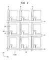
- FIG. 1 is a configuration diagram showing an embodiment of a circuit formed in a liquid crystal display region of a surface on a liquid crystal side of one substrate SUB1 of the substrates disposed to be opposed to each other via the liquid crystal of a liquid crystal display device.
- source signal lines SL extending in a y direction and disposed in parallel in an x direction and gate signal lines GL isolated from the source signal lines SL, extending in the x direction and disposed in parallel in the y direction are provided. Further, a rectangular region surrounded by these signal lines corresponds to a region of a pixel (shown by a dotted frame in FIG. 1 ). Accordingly, each of the pixels is disposed in a matrix pattern, and the liquid crystal display region is configured from the pixel group.
- a pixel electrode PX constituted of, for example, a transparent electrode is formed across a most part of each pixel region, and the pixel electrode PX is connected to, for example, the source signal line SL adjacent on the left side in FIG. 1 via a thin film transistor TFT.
- a thin film transistor TFT By the on/off driving of the thin film transistor TFT, supplying and non-supplying of the signal from the source signal line SL to the pixel electrode PX are controlled.
- a gate electrode GT formed of an extended portion of the gate signal line GL is disposed above the semiconductor layer, and thus the thin film transistor TFT has a so-called top-gate type MIS (Metal Insulator Semiconductor) structure.
- MIS Metal Insulator Semiconductor
- the thin film transistors TFT of each pixel of a pixel column are turned on, and by supplying a video signal to each of the source signal lines SL in accordance with the turning-on timing, the voltage of the video signal is applied to the pixel electrode PX in each pixel of the pixel column.
- the liquid crystal display device shown in this embodiment has another substrate (not shown) disposed to be opposed to the substrate SUB1 via the liquid crystal, and a counter electrode common to each pixel is formed on the surface on the liquid crystal side of this substrate.
- This counter electrode is constituted of, for example, a transparent electrode, and a signal including a voltage to be a reference for the signal (video signal) supplied to the source signal line SL is supplied to the counter electrode.
- An electric field generated by a difference in potential between the pixel electrode PX and the counter electrode is applied to the liquid crystal, so that the molecules of the liquid crystal are oriented.
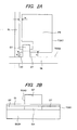
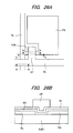
- FIG. 2A is a view showing one pixel extracted from the pixels shown in FIG. 1 .
- FIG. 2B is a cross-sectional view taken along the line b-b of FIG. 2A .
- the source signal line SL, a source region portion ST of the thin film transistor TFT, a channel region portion CH (portion directly below the gate electrode GT), a drain region portion DT, and the pixel electrode PX are formed from a first transparent oxide layer TOX1 formed integrally in the same layer.
- the channel region portion CH is formed as a film with a low carrier concentration and a high sheet resistance (semiconductor layer), and the forming regions of the source signal line SL, the source region portion ST of the thin film transistor TFT, the drain region portion DT, and the pixel electrode PX are formed as a film with a high carrier concentration and a low sheet resistance (conductive layers).
- these components can be formed so that the sheet resistance becomes higher in order of the source signal line SL and the pixel electrode PX ⁇ the source region portion ST and the drain region portion DT ⁇ the channel region portion CH.
- these components can be formed so that the sheet resistance becomes higher in order of the source signal line SL ⁇ the pixel electrode PX, the source region portion ST and the drain region portion DT ⁇ the channel region portion CH.
- carrier concentration of the pixel electrode PX can be reduced to a relatively low level, and thus the pixel electrode PX can be formed without deteriorating the transparency thereof.
- the source signal line SL and the pixel electrode PX thus configured are integrally formed from the first transparent oxide layer TOX1 in the same layer, the interval therebetween (shown by w in FIG. 2A ) can be reduced to the minimum. This is because, compared with the case where the source signal line SL and the pixel electrode PX are formed in different processes, the problem that the interval therebetween becomes large due to the limit of mask alignment can be solved. As a result, a configuration capable of achieving the improvement of the aperture ratio of the pixel can be realized.
- the gate signal line GL and the gate electrode GT of the thin film transistor TFT are integrally formed in the same layer from, for example, a second transparent oxide layer TOX2 such as ITO (Indium Tin Oxide) or ZnO with a high carrier concentration and a low sheet resistance.
- the gate signal line GL and the gate electrode GT are not limited to the transparent oxide layer as describe above, and can be formed from, for example, a metal layer. This is because, when the electric resistance of the gate signal line GL is desired to be further reduced, it is appropriate to use a metal layer made of a material corresponding thereto.
- the first transparent oxide film TOX1 is formed on the surface of the substrate SUB1, and the upper surface thereof is covered with an insulating film GI.
- the gate electrode GT is disposed above the channel region portion CH of the first transparent oxide film TOX1 via the insulating film GI.
- the insulating film GI functions as a gate insulating film of the thin film transistor TFT.
- the region with a high carrier concentration and the region with a low carrier concentration are separately formed, and the former is formed as a conductive layer and the latter is formed as a semiconductor layer. Therefore, before describing the manufacturing method of the liquid crystal display device, several embodiments in which the region with a high carrier concentration and the region with a low carrier concentration are selectively and separately formed in the transparent oxide layer TOX will be described.
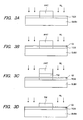
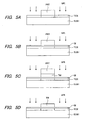
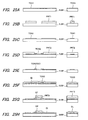
- FIG. 3A to FIG. 3D are views each showing an embodiment in which a region with a high carrier concentration is selectively formed in a transparent oxide layer TOX formed on the upper surface of the substrate SUB1.
- the transparent oxide layer TOX is formed on the upper surface of the substrate SUB 1, and a photoresist film PRT is formed as a mask on the region of the surface of the transparent oxide layer TOX other than the region where the carrier concentration is to be increased.
- a laser light RL is irradiated to the transparent oxide layer TOX.
- this laser light RL for example, KrF excimer laser is preferably used, but other light sources are also available.
- the region of the transparent oxide layer TOX exposed from the photoresist film PRT is modified in terms of crystallinity by the light, and can be formed as a region with an improved carrier concentration.
- FIG. 3B shows another embodiment in which the region with a high carrier concentration is selectively formed in the transparent oxide layer TOX by the light irradiation, and this case is different from the case of FIG. 3A in that the insulating film GI is formed on the surface of the transparent oxide layer TOX in advance and the laser light RL is irradiated to the transparent oxide layer TOX through the insulating film GI.
- FIG. 3C shows another embodiment in which the region with a high carrier concentration is selectively formed in the transparent oxide layer TOX by the light irradiation, and this case is different from the case of FIG. 3B in that the transparent oxide layer TOX is covered with the insulating film GI, and the laser light RL is irradiated to the transparent oxide layer TOX with using an electrode TM formed on a part the insulating film GI and the photoresist film PRT stacked on the electrode TM as a mask.
- FIG. 3D shows another embodiment in which the region with a high carrier concentration is selectively formed in the transparent oxide layer TOX by the light irradiation, and this case is different from the case of FIG. 3C in that, after the photoresist film PRT for forming the electrode TM shown in FIG. 3C is removed, a laser light PL is irradiated to the transparent oxide layer TOX with using the electrode TM as a mask.
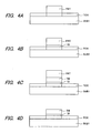
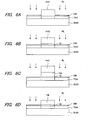
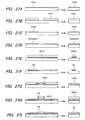
- FIG. 4A to FIG. 4D are views each showing another embodiment in which a region with a high carrier concentration is selectively formed in a transparent oxide layer TOX formed on the upper surface of the substrate SUB1.
- the transparent oxide layer TOX is formed on the upper surface of the substrate SUB 1, and a photoresist film PRT is formed as a mask on the region of the surface of the transparent oxide layer TOX other than the region where the carrier concentration is to be increased.
- the region of the transparent oxide layer TOX exposed from the photoresist film PRT is modified in terms of crystallinity by the thermal annealing, and can be formed as a region with an improved carrier concentration.
- FIG. 4B shows another embodiment in which the region with a high carrier concentration is selectively formed in the transparent oxide layer TOX by the thermal annealing, and this case is different from the case of FIG. 4B in that the thermal annealing is performed while leaving the insulating film GI selectively formed on the surface of the transparent oxide layer TOX and the photoresist film PRT formed on an upper surface of the insulating film GI and used for selectively forming the insulating film GI.
- FIG. 4C shows another embodiment in which the region with a high carrier concentration is selectively formed in the transparent oxide layer TOX by the thermal annealing, and this case is different from the case of FIG. 4C in that the thermal annealing is performed while leaving a stacked body of the insulating film GI and the electrode TM selectively formed on the surface of the transparent oxide layer TOX and the photoresist film PRT formed on an upper surface of the stacked body and used for forming the electrode TM and the insulating film GI.
- FIG. 4D shows another embodiment in which the region with a high carrier concentration is selectively formed in the transparent oxide layer TOX by the thermal annealing, and this case is different from the case of FIG. 4C in that thermal annealing is performed in a state where the photoresist film PRT used for forming a stacked body of the insulating film GI and the electrode TM selectively formed on the surface of the transparent oxide layer TOX is removed.
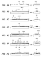
- FIG. 5A to FIG. 5D are views each showing another embodiment in which a region with a high carrier concentration is selectively formed in a transparent oxide layer TOX formed on the upper surface of the substrate SUB1.
- the transparent oxide layer TOX is formed on the upper surface of the substrate SUB 1, and a photoresist film PRT is formed as a mask on the region of the surface of the transparent oxide layer TOX other than the region where the carrier concentration is to be increased.
- an impurity ion NPI is implanted into the transparent oxide layer TOX.
- An n type impurity or a p type impurity is used for the impurity ion NPI according to need.
- the region of the transparent oxide layer TOX exposed from the photoresist film PRT can be formed as a region with an improved carrier concentration by the implantation of the impurity ion NPI.
- FIG. 5B is a view showing another embodiment in which the region with a high carrier concentration is formed in the transparent oxide layer TOX formed on the upper surface of the substrate SUB1 by the implantation of the impurity ion NPI, and this case is different from the case of FIG. 5A in that the insulating film GI is formed on the surface of the transparent oxide layer TOX in advance and the implantation of the impurity ion NPI is performed to the transparent oxide layer TOX through the insulating film GI.
- FIG. 5C shows another embodiment in which the region with a high carrier concentration is formed in the transparent oxide layer TOX by the implantation of the impurity ion NPI, and this case is different from the case of FIG. 5B in that the transparent oxide layer TOX is covered with the insulating film GI, and the implantation of the impurity ion NPI is performed to the transparent oxide layer TOX, with using the electrode TM formed on a part of the region of the insulating film GI and the photoresist film PRT stacked on the electrode TM as a mask.
- FIG. 5D shows another embodiment in which the region with a high carrier concentration is formed in the transparent oxide layer TOX by the implantation of the impurity ion NPI, and this case is different from the case of FIG. 5C in that, after the photoresist film PRT for forming the electrode TM shown in FIG. 5C is removed, the implantation of the impurity ion NPI is performed to the transparent oxide layer TOX with using the electrode TM as a mask.
- FIG. 6A to FIG. 6D are views each showing another embodiment in which a region with a high carrier concentration is selectively formed in a transparent oxide layer TOX formed on the upper surface of the substrate SUB1.
- the transparent oxide layer TOX is formed on the upper surface of the substrate SUB 1, and a photoresist film PRT is formed as a mask on the region of the surface of the transparent oxide layer TOX other than the region where the carrier concentration is to be increased.
- a dopant material DM containing an n type or p type impurity is deposited on the surface of the transparent oxide layer TOX exposed from the mask.
- the irradiation of a laser light RL is performed to the transparent oxide layer TOX.
- the laser light RL for example, the KrF excimer laser is preferably used, but other light sources are also available.
- the dopant material DM is diffused in the region of the transparent oxide layer TOX exposed from the photoresist film PRT, and the region can be formed as a region with an improved carrier concentration.
- FIG. 6B shows another embodiment in which the region with a high carrier concentration is formed in the transparent oxide layer TOX by the diffusion of the dopant material DM, and this case is different from the case of FIG. 6A in that the irradiation (or thermal annealing) of the laser light RL is performed while leaving the insulating film GI selectively formed on the surface of the transparent oxide layer TOX and the photoresist film PRT formed on the upper surface of the insulating film GI and used for selectively forming the insulating film GI.
- FIG. 6C shows another embodiment in which the region with a high carrier concentration is formed in the transparent oxide layer TOX by the diffusion of the dopant material DM, and this case is different from the case of FIG. 6B in that the irradiation (or thermal annealing) of the laser light RL is performed while leaving the stacked body of the insulating film GI and the electrode TM selectively formed on the surface of the transparent oxide layer TOX and the photoresist film PRT formed on the upper surface of the stacked body and used for forming the electrode TM and the insulating film GI.
- FIG. 6D shows another embodiment in which the region with a high carrier concentration is formed in the transparent oxide layer TOX by the diffusion of the dopant material DM, and this case is different from the case of FIG. 6C in that the irradiation (or thermal annealing) of the laser light RL is performed in a state where the photoresist film PRT used for forming a stacked body of the insulating film GI and the electrode TM selectively formed on the surface of the transparent oxide layer TOX is removed.
- any of the processes shown in FIG. 3 to FIG. 6 can be adopted.
- the method using the irradiation of the laser light is taken as an example.
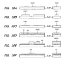
- FIG. 8A to FIG. 8G are process drawings showing an embodiment of the manufacturing method of the liquid crystal display device.
- FIG. 8A to FIG. 8G are process drawings in one pixel of the liquid crystal display region, and the process drawings on the left side of FIG. 8A to FIG. 8G correspond to the cross sections of the line L-L in FIG. 7 , and the process drawings on the right side of FIG. 8A to FIG. 8G correspond to the cross sections of the line R-R in FIG. 7 .
- the pixel shown in FIG. 7 is the same pixel as that shown in FIG. 2 .
- the LDD region portion functions to buffer the electric field with the gate electrode GT.
- the substrate SUB1 made of, for example, glass is prepared, and a first transparent oxide layer TOX1 with a high resistance made of, for example, ZnO or the like and a first insulating film GI1 made of, for example, SiO 2 or the like are sequentially deposited on the surface (surface on the liquid crystal side) of the substrate SUB1.
- the first insulating film GI1 functions as a gate insulating film in the forming region of the thin film transistor TFT.
- a first photoresist film PRT1 is formed on the entire upper surface of the first insulating film GI1, and the first photoresist film PRT1 is formed into a predetermined pattern.
- the patterned first photoresist film PRT1 is formed in the region where the source signal line SL, the thin film transistor TFT connected to the source signal line SL, and the pixel electrode PX connected to the thin film transistor TFT in the pixel shown in FIG. 7 are to be formed, and further, the patterned first photoresist film PRT1 is formed so as to have regions with different heights such as a higher region and a lower region. More specifically, the higher region is disposed on the forming region of the channel region portion of the thin film transistor TFT and the so-called LDD regions (field buffer region) on both sides of the channel region portion, and the lower region is disposed on the portion other than the forming region.
- LDD regions field buffer region
- the first photoresist film PRT1 having the higher region and the lower region is formed by, for example, exposing the first photoresist film PRT1 to light by using three types of photomasks each having different translucency such as a light-shielding mask, a so-called semi-translucent mask, and a translucent mask.
- the first photoresist film PRT1 as described above can be formed by the exposure using a so-called half-tone mask or a gray-tone mask.
- the first insulating film GI1 and the first transparent oxide layer TOX1 below the first insulating film GI1 exposed from the mask are sequentially etched, and the surface of the substrate SUB1 is exposed.
- the stacked body of the first transparent oxide layer TOX and the first insulating film GI1 is left on the forming regions of the source signal line SL, the thin film transistor TFT connected to the source signal line SL, and the pixel electrode PX connected to the thin film transistor TFT.
- the surface of the first photoresist film PRT1 is removed by an appropriate amount toward the bottom surface thereof.
- the first photoresist film PRT1 is completely removed in the forming regions of the source signal line SL, the thin film transistor TFT (except for the channel region portion and the LDD region portion thereof) connected to the source signal line SL, and the pixel electrode PX connected to the thin film transistor TFT, and is left only in the forming region of the channel region portion and the LDD region portion of the thin film transistor TFT.
- the first transparent oxide layer TOX1 is modified in terms of crystallinity. This is for the purpose of improving the carrier concentration and lowering the resistance of the first transparent oxide layer TOX1.
- the irradiation of the laser light RL is blocked in the portion where the first photoresist film PRT1 is formed, so that the first transparent oxide layer TOX1 directly below the first photoresist film PRT1 is allowed to maintain its high resistance.
- the carrier concentration is increased in each of the forming regions of the source signal line SL, the thin film transistor TFT connected to the source signal line SL (except for the portions of the channel region portion and the LDD region portion thereof), and the pixel electrode PX connected to the thin film transistor TFT to convert the regions into electrically conductive regions, and the semiconductor region with a low carrier concentration is left in the portion of the channel region of the thin film transistor TFT.
- the first photoresist film PRT1 is all removed.
- a second insulating film GI2 made of, for example, SiO 2 and a second transparent oxide layer TOX2 made of, for example, ITO (Indium Tin Oxide) are sequentially deposited.
- the second insulating film GI2 functions as an interlayer insulating film of the later-described gate signal line GL for the source signal line SL.
- a second photoresist film PRT2 is formed on the upper surface of the second transparent oxide layer TOX2, and this second photoresist film PRT2 is formed into a predetermined pattern. That is, the second photoresist film is left in each of the forming regions of the gate signal line GL and the gate electrode GT of the thin film transistor TFT connected to the gate signal line GL.
- the forming region of the gate electrode GT is a portion directly above the channel region portion of the thin film transistor TFT, and the LDD regions on both sides of the channel region are excluded.
- the second transparent oxide layer TOX2 exposed from the second photoresist film PRT2 is etched, and the gate signal line SL and the gate electrode T are formed from the left second transparent oxide layer TOX2.
- the laser light RL is irradiated to the first transparent oxide layer TOX1 through the second insulting film GI2 and the first insulating film GI1.
- the carrier concentration is increased in the LDD regions LD on both sides of the channel region portion CH of the thin film transistor TFT.
- the carrier concentration is further increased also in the portion of the first transparent oxide layer TOX1 where the carrier concentration has been increased in the process 3
- the LDD region LD is formed as a region with a relatively small conductivity.
- the second photoresist film PRT2 is all removed. Thereafter, an alignment film (not shown) is formed over the surface of the substrate SUB1, thereby completing the process.
- the liquid crystal display region on the surface on the liquid crystal side of the substrate SUB1 can be fabricated by the so-called two-photo process using the first photoresist film PRT1 and the second photoresist film PRT2.
- the first photoresist film PRT1 functions as a mask at the time of the sequential selective etching for forming the stacked body of the first transparent oxide layer TOX1 and the first insulating film GI1 and also as a mask at the time of selectively forming the region with a high carrier concentration in the first transparent oxide layer TOX1, respectively.
- the application of the photolithography technique is required only once, and therefore, the number of processes can be reduced significantly.
- FIG. 9A to FIG. 9G are process drawings showing another embodiment of the manufacturing method of the liquid crystal display device.
- FIG. 9A to FIG. 9G correspond to FIG. 8A to FIG. 8G
- the process drawings on the left side of FIG. 9A to FIG. 9G correspond to the cross sections of the line L-L in FIG. 7
- the process drawings on the right side of FIG. 9A to FIG. 9G correspond to the cross sections of the line R-R in FIG. 7 .
- the substrate SUB1 is prepared, and a first transparent oxide layer TOX1 with a high resistance made of, for example, ZnO or the like and a first insulating film GI1 made of, for example, SiO 2 or the like are sequentially deposited on the surface of the substrate SUB1 (surface on the liquid crystal side).
- a first transparent oxide layer TOX1 with a high resistance made of, for example, ZnO or the like and a first insulating film GI1 made of, for example, SiO 2 or the like are sequentially deposited on the surface of the substrate SUB1 (surface on the liquid crystal side).
- a first photoresist film PRT1 is formed on the entire upper surface of the first insulating film GI1, and the first photoresist film PRT1 is formed into a predetermined pattern.
- the patterned first photoresist film PRT1 is formed in each of the forming regions of the source signal line SL, the thin film transistor TFT connected to the source signal line SL, and the pixel electrode PX connected to the thin film transistor TFT in the pixel shown in FIG. 7 , and further, the patterned first photoresist film PRT1 is formed so as to have regions with different heights such as a higher region and a lower region. More specifically, the lower region is disposed on the portion of the source signal line SL and the higher region is disposed on the portion other than the portion.
- the first insulating film GI1 and the first transparent oxide layer TOX1 below the first insulating film GI1 exposed from the mask are sequentially etched, and the surface of the substrate SUB1 is exposed.
- the stacked body of the first transparent oxide layer TOX1 and the first insulating film GI1 is left in the forming regions of the source signal line SL, the thin film transistor TFT connected to the source signal line SL, and the pixel electrode PX connected to the thin film transistor TFT.
- the surface of the first photoresist film PRT1 is removed by an appropriate amount toward the bottom surface thereof.
- the first photoresist film PRT1 is completely removed in the forming region of the source signal line SL, and is left in only each of the forming regions of the channel region portion of the thin film transistor TFT, the LDD region portion adjacent to the channel region portion and disposed on the source signal line SL side, and the pixel electrode PX.
- the first transparent oxide layer TOX1 is modified in terms of crystallinity.
- the irradiation of the laser light RL is blocked in the portion where the first photoresist film PRT1 is formed, so that the first transparent oxide layer TOX1 directly below the first photoresist film PRT1 is allowed to maintain its high resistance.
- the first photoresist film PRT1 is all removed.
- a second insulating film GI2 made of, for example, SiO 2 and a second transparent oxide layer TOX2 made of, for example, ITO (Indium Tin Oxide) are sequentially deposited.
- the second photoresist film PRT2 is formed on the upper surface of the second transparent oxide layer TOX2, and this second photoresist film PRT2 is formed into a predetermined pattern. That is, the second photoresist film is left in each of the forming regions of the gate signal line GL and the gate electrode GT of the thin film transistor TFT connected to the gate signal line GL.
- the forming region of the gate electrode GT is a portion directly above the channel region portion of the thin film transistor TFT, and the LDD region LD on the source signal line SL side adjacent to the channel region portion is excluded.
- the second transparent oxide layer TOX2 exposed from the second photoresist film PRT2 is etched, and the gate signal line SL and the gate electrode GT are formed from the left second transparent oxide layer TOX2.
- the second photoresist film PRT2 is left as it is, and the laser light RL is irradiated to the first transparent oxide layer TOX1 through the second insulting film GI2 and the first insulating film GI1.
- the carrier concentration is increased in the LDD region LD adjacent to the channel region portion of the thin film transistor TFT.
- the carrier concentration is further increased also in the portion of the first transparent oxide layer TOX1 where the carrier concentration has been increased in the process 3
- the LDD region LD is formed as a region with a relatively small conductivity.
- the portion of the pixel electrode PX adjacent to the channel region portion of the thin film transistor TFT is formed as a region with a relatively small conductivity. This is because, since the pixel electrode PX functions as an electrode generating an electric field with another electrode (not shown) (counter electrode), the conductivity of the pixel electrode PX can be set to a relatively small value. Further, although the first transparent oxide layer TOX1 such as ZnO is metallized and is no longer transparent when the carrier concentration is much increased, the carrier concentration of the pixel electrode PX can be controlled to an extent capable of maintaining its transparency.
- the method by the irradiation of the laser light RL is used when a region with a high carrier concentration is formed in the first transparent oxide layer TOX1 as an embodiment.
- the methods shown in FIG. 3 to FIG. 6 or other methods can be used as described above.
- a method where the irradiation of the laser light RL is performed in a state where the insulating film GI is not formed on the surface of the transparent oxide layer TOX is included in the methods shown in FIG. 3 to FIG. 6 . Therefore, in the manufacturing methods shown in FIG. 8 and FIG. 9 , the process in which a region with a high carrier concentration is first formed in the transparent oxide layer TOX in a state where the insulating film GI is not formed, and then the insulating film GI is formed can also be applied.
- a photoresist film is directly drawn or evaporated using a mask in the region other than the array end region required for the contact, and the insulating film of the corresponding array end portion is etched and removed.
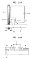
- FIG. 10A is a plan view showing another embodiment of the configuration of a pixel of a display device according to the present invention, and FIG. 10A corresponds to FIG. 2A .
- a source signal line SL, a thin film transistor TFT connected to the source signal line SL, and a pixel electrode PX connected to the thin film transistor TFT are formed in each region separately formed on the surface of a first transparent oxide layer TOX1, which is formed across the entire surface of a substrate SUB1.
- FIG. 10A The configuration of FIG. 10A is different from that of FIG. 2A in that a first transparent oxide layer TOX1 with a low carrier concentration (effectively functions as an insulator) is formed on the surface of the substrate SUB1 even in the region other than the forming regions of the source signal line SL, the thin film transistor TFT, and the pixel electrode PX. More specifically, in this configuration, the first transparent oxide layer TOX1 formed in the entire region of the surface of the substrate SUB1 is not selectively etched.
- the source signal line SL and the pixel electrode PX are formed integrally in the same layer from the first transparent oxide layer TOX1, the interval therebetween (shown by w in FIG. 10A ) can be reduced to the minimum, and a configuration capable of achieving the improvement of the aperture ratio of the pixel can be realized.
- the first transparent oxide layer TOX1 thus configured can be formed by forming a photoresist film as usual at the time of forming the first photoresist film PRT1 in the manufacturing method shown in FIG. 8A to FIG. 8G or FIG. 9A to FIG. 9G in the first embodiment, and it is not necessary to form, for example, the half-exposed photoresist film having a difference in level on its surface.
- FIG. 10B corresponding to the process shown in FIG. 8C and showing the process in the section of the line b-b in FIG. 10A
- a photoresist film covering the channel region portion CH of the thin film transistor TFT and the LDD region portions LD on both sides of the channel region portion CH and a photoresist film covering a region other than the forming regions of the source signal line SL, the thin film transistor TFT, and the pixel electrode PX are formed from the first photoresist film PRT1, and thereafter, the process shown in FIG. 8 is to be performed.
- the manufacturing method shown in FIG. 9 is adapted.
- the display device having the configuration as described above can achieve the advantage that the difference in level on the surface facing the liquid crystal can be reduced.
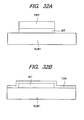
- FIG. 11A is a plan view showing another embodiment of the configuration of a pixel of a display device according to the present invention, and FIG. 11A corresponds to FIG. 7 and FIG. 10A . Also, FIG. 11B is a cross-sectional view taken along the line b-b in FIG. 11A .
- FIG. 11A The configuration of FIG. 11A is different from those of FIG. 7 and FIG. 10A in that a main source signal line SL' is made of, for example, a metal layer with a low electric resistance and is formed independently from other members.
- main line a source signal line SL made from a first transparent oxide layer TOX1 stacked across the entire region is formed for the source signal line SL'.
- the configuration shown in FIG. 7 or 10A is stacked over the surface of the substrate SUB1 on which the source signal line SL' is formed, so that the source signal line SL shown in FIG. 7 or FIG. 10A is overlapped and formed on the source signal line SL'.
- the source signal line SL constituted of the first transparent oxide layer TOX1 is formed so as to be connected to the source signal line SL' made of a metal layer formed below the source signal line SL, the electric resistance can be significantly reduced.
- FIG. 11 shows that the source signal line SL constituted of the first transparent oxide layer TOX1 and the source signal line SL' constituted of a metal layer have the center axes matched with each other and approximately the same widths.
- the source signal line SL' constituted of a metal layer can be configured to have the width smaller than the width of the source signal line SL constituted of the first transparent oxide layer TOX1. This is because the electric resistance of the source signal line can be sufficiently reduced as a whole.
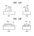
- FIG. 12A and FIG. 12B are process drawings showing a process of a manufacturing method in the case where the source signal line SL' is formed on the surface of the substrate SUB1.
- FIG. 12A and FIG. 12B are cross-sectional views taken along the line L-L in FIG. 11A
- the process drawings on the right side thereof are cross-sectional views taken along the line R-R in FIG. 11A .
- a metal layer MT is formed on the entire region of the surface of the substrate SUB1, and then the metal layer MT is selectively etched with using a photoresist film PRT patterned on the surface of the metal layer MT as a mask, thereby forming the source signal line SL'.
- the first transparent oxide layer TOX1 made of, for example, ZnO and the insulating film GI made of, for example, SiO 2 are sequentially stacked.
- This process corresponds to, for example, the process shown in FIG. 8A , and thereafter, the processes shown in FIG. 8B to FIG. 8G are performed, thereby completing the configuration shown in FIG. 11A and FIG. 11B .
- the source signal line SL constituted of the first transparent oxide layer TOX1 is stacked across the entire region of the source signal line SL'.
- the embodiment is not limited to this, and the configuration in which the source signal line SL is stacked only on a part of the source signal line SL' is also possible.
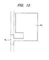
- the configuration may be such that the source signal line SL is stacked only on the source signal line SL' in the vicinity of the thin film transistor TFT. This is because, since the source signal line SL' is made of a metal layer, the electric resistance thereof can be sufficiently reduced by itself.
- the sequential stacked body of the first transparent oxide layer TOX1 and the insulating film GI is formed to have a pattern shown in FIG. 13 , and the portion formed as the source signal line SL is placed only in the vicinity of the forming region of the thin film transistor TFT.
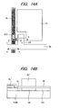
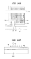
- FIG. 14A is a plan view showing another embodiment of the configuration of a pixel of a display device according to the present invention, and FIG. 14A corresponds to FIG. 11A .
- FIG. 14B is a cross-sectional view taken along the line b-b in FIG. 14A .
- FIG. 14A similarly has a main source signal line SL', but it is different from the configuration of FIG. 11A in that the source signal line SL' is disposed on the source signal line SL.
- the source signal line SL' is made of, for example, a metal layer, and the source signal line SL constituted of the first transparent oxide layer TOX1 is formed and stacked on the source signal line SL', and therefore, the electric resistance can be significantly reduced.
- the source signal line SL constituted of the first transparent oxide layer TOX1 and the source signal line SL' constituted of a metal layer have the center axes matched with each other and approximately the same widths.
- the source signal line SL' constituted of a metal layer can be configured to have the width smaller than the width of the source signal line SL constituted of the first transparent oxide layer TOX1. This is because the electric resistance of the source signal line can be sufficiently reduced as a whole.
- FIG. 15A to FIG. 15H are process drawings showing an embodiment of the manufacturing method of the pixel of the display device, and process drawings on the left side in FIG. 15A to FIG. 15H are cross-sectional views taken along the line L-L in FIG. 14A and process drawings on the right side in FIG. 15A to FIG. 15H are cross-sectional views taken along the line R-R in FIG. 14A .
- the substrate SUB1 is prepared, and a first transparent oxide layer TOX1 with a high resistance made of, for example, ZnO or the like and a first insulating film GI1 made of, for example, SiO 2 the like are sequentially deposited on the surface of the substrate SUB1.
- a first transparent oxide layer TOX1 with a high resistance made of, for example, ZnO or the like and a first insulating film GI1 made of, for example, SiO 2 the like are sequentially deposited on the surface of the substrate SUB1.
- the first photoresist film PRT1 is formed on the entire upper surface of the first insulating film GI1, and the first photoresist film PRT1 is formed into a predetermined pattern.
- the patterned first photoresist film PRT1 is formed in each of the forming regions of the source signal line SL, the thin film transistor TFT connected to the source signal line SL, and the pixel electrode PX connected to the thin film transistor TFT in the pixel shown in FIG. 14A , and further, the patterned first photoresist film PRT1 is formed so as to have regions with different heights such as a higher region and a lower region. More specifically, the higher region is disposed on the forming region of the channel region portion of the thin film transistor TFT and the so-called LDD regions on both sides of the channel region portion, and the lower region is disposed on the portion other than the forming region.
- the first insulating film GI1 and the first transparent oxide layer TOX1 below the first insulating film GI1 exposed from the mask are sequentially etched, and the surface of the substrate SUB1 is exposed.
- the stacked body of the first transparent oxide layer TOX1 and the first insulating film GI1 is left in the forming regions of the source signal line SL, the thin film transistor TFT connected to the source signal line SL, and the pixel electrode PX connected to the thin film transistor TFT.
- the surface of the first photoresist film PRT1 is removed by an appropriate amount toward the bottom surface thereof, so that the first photoresist film PRT1 is left only in the forming region of the channel region portion of the thin film transistor TFT and the LDD region portions on both sides of the channel region portion.
- the first transparent oxide layer TOX1 is modified in terms of crystallinity and the carrier concentration thereof is improved.
- the irradiation of the laser light RL is blocked in the portion where the first photoresist film PRT1 is formed, so that the first transparent oxide layer TOX1 directly below the first photoresist film PRT1 is allowed to maintain its high resistance.
- the first photoresist film PRT1 is all removed.
- a second photoresist film PRT2 is formed over the surface of the substrate SUB1, and the second photoresist film PRT2 is patterned, thereby forming the second photoresist film PRT2 removed in the portion where the source signal line SL is to be formed and left in the other portion.
- the first insulating film GI1 exposed from the second photoresist film PRT2 is selectively etched, and the portion (portion of the source signal line SL) of the first transparent oxide layer TOX1 modified in terms of crystallinity is exposed.
- a metal is evaporated from above the second photoresist film PRT2, and the second photoresist film PRT2 is peeled.
- This is a so-called lift off method, and a metal layer MT is formed on the portion (portion of the source signal line SL) of the first transparent oxide layer TOX1 modified in terms of crystallinity.
- This metal layer MT corresponds to the source signal line SL' formed and stacked on the source signal line SL.
- the second photoresist film PRT2 is removed, and the second insulating film GI2 made of, for example, SiO 2 and the second transparent oxide layer TOX2 made of, for example, an ITO film are sequentially formed.
- a third photoresist film PRT3 is formed over the surface of the substrate SUB1, and the third photoresist film PRT3 is patterned, thereby forming the third photoresist film PRT3 left in the portion where the gate signal line GL and the gate electrode GT of the thin film transistor TFT are to be formed.
- the second transparent oxide layer TOX2 exposed from the mask is selectively etched, and the second insulating film GI2 below the second transparent oxide layer TOX2 is exposed.
- the laser light RL is irradiated to the first transparent oxide layer TOX1 through the second insulting film GI2.
- the region between the channel region portion of the thin film transistor TFT directly below the gate electrode GT and the source signal line SL' is modified in terms of crystallinity, so that the LDD region portion LD is formed. Accordingly, in the modification in terms of crystallinity by the laser light RL in this process, it is necessary to reduce the modification level in comparison with that in the modification by the laser light RL in the process 3.
- the third photoresist film PRT3 is removed.
- FIG. 16A to FIG. 16H are process drawings showing another embodiment of the manufacturing method of the pixel of the display device, and process drawings on the left side in FIG. 16A to FIG. 16H are cross-sectional views taken along the line L-L in FIG. 14A and process drawings on the right side in FIG. 16A to FIG. 16H are cross-sectional views taken along the line R-R in FIG. 14A .
- the substrate SUB1 is prepared, and a first transparent oxide layer TOX1 with a high resistance made of, for example, ZnO or the like and a first insulating film GI1 made of, for example, SiO 2 or the like are sequentially deposited on the surface of the substrate SUB1.
- a first transparent oxide layer TOX1 with a high resistance made of, for example, ZnO or the like and a first insulating film GI1 made of, for example, SiO 2 or the like are sequentially deposited on the surface of the substrate SUB1.
- the first photoresist film PRT1 is formed on the entire upper surface of the first insulating film GI1, and the first photoresist film PRT1 is formed into a predetermined pattern.
- the patterned first photoresist film PRT1 is formed in each of the forming regions of the source signal line SL, the thin film transistor TFT connected to the source signal line SL, and the pixel electrode PX connected to the thin film transistor TFT in the pixel shown in FIG. 14A , and further, the patterned first photoresist film PRT1 is formed so as to have regions with different heights such as a higher region and a lower region. More specifically, the higher region is disposed on the forming region of the channel region portion of the thin film transistor TFT and the forming region of the LDD regions on both sides of the channel region portion, and the lower region is disposed on the portion other than the forming regions.
- the first insulating film GI1 and the first transparent oxide layer TOX1 below the first insulating film GI1 exposed from the mask are sequentially etched, and the surface of the substrate SUB1 is exposed.
- the stacked body of the first transparent oxide layer TOX1 and the first insulating film GI1 is left in the forming regions of the source signal line SL, the thin film transistor TFT connected to the source signal line SL, and the pixel electrode PX connected to the thin film transistor TFT.
- the surface of the first photoresist film PRT1 is removed by an appropriate amount toward the bottom surface thereof, so that the first photoresist film PRT1 is left only in the forming region of the channel region portion of the thin film transistor TFT and the LDD region portions on both sides of the channel region portion.
- the first transparent oxide layer TOX1 is modified in terms of crystallinity and the carrier concentration thereof is improved.
- the irradiation of the laser light RL is blocked in the portion where the first photoresist film PRT1 is formed, so that the first transparent oxide layer TOX1 directly below the first photoresist film PRT1 is allowed to maintain its high resistance.
- the first insulating film GI1 is removed.
- metal is evaporated over the entire region of the surface of the substrate SUB1, thereby forming a metal layer MT.
- a second photoresist film PRT2 is formed over the entire region of the surface of the substrate SUB1, and then the second photoresist film PRT2 is patterned, thereby leaving the second photoresist film PRT2 in the forming region of the source signal line SL.
- the metal layer MT exposed from the mask is selectively etched.
- the second photoresist film PRT2 is removed, and the left metal layer MT is formed as the source signal line SL'.
- the second insulating film GI2 made of, for example, SiO 2 and the second transparent oxide layer TOX2 made of, for example, an ITO film are sequentially formed.
- a third photoresist film PRT3 is formed over the surface of the substrate SUB1, and then the third photoresist film PRT3 is patterned, thereby forming the third photoresist film PRT3 left in the portion where the gate signal line GL and the gate electrode GT of the thin film transistor TFT are to be formed.
- the second transparent oxide layer TOX2 exposed from the mask is selectively etched, and the second insulating film GI2 below the second transparent oxide layer TOX2 is exposed.
- the laser light RL is irradiated to the first transparent oxide layer TOX1 through the second insulting film GI2.
- the region between the channel region portion of the thin film transistor TFT directly below the gate electrode GT and the source signal line SL' is modified in terms of crystallinity, so that the LDD region portion LD is formed. Accordingly, in the modification in terms of crystallinity by the laser light RL in this process, it is necessary to reduce the modification level in comparison with that in the modification by the laser light RL in the process 3.
- the third photoresist film PRT3 is removed.
- FIG. 17A is a plan view showing another embodiment of the configuration of a pixel of a display device according to the present invention.
- FIG. 17B is a cross-sectional view taken along the line b-b in FIG. 17A .
- the pixel shown in FIG. 17 is configured to have a pixel electrode PX and a counter electrode CT which generates an electric field with the pixel electrode PX in a pixel region on a liquid crystal side of a substrate SUB 1.
- the pixel electrode PX is configured to be supplied with a video signal from a source signal line SL via a thin film transistor TFT, and has the approximately same configuration as that described in the embodiments above.
- the counter electrode CT is disposed and overlapped on the pixel electrode PX via an insulating film (for example, first insulating film), and is configured as a comb-shaped electrode including a number of electrodes disposed in parallel.
- an insulating film for example, first insulating film
- the counter electrode CT is integrally formed with a common signal line CL, which extends approximately in parallel with the gate signal line GL, at the mid-portion of each electrode, and a reference voltage serving as a reference for the video signal is applied to the comb-shaped electrode through the common signal line CL.
- the comb-shaped electrode integrally formed with the common signal line CL is in the same layer as the gate signal line GL, and for example, the comb-shaped electrode is formed at the same time of forming the gate signal line GL.
- the molecules of the liquid crystal disposed for the pixel thus configured via an alignment film are oriented by the electric field generated between the pixel electrode PX and the counter electrode CT.
- the entire region of the pixel electrode PX is modified in terms of crystallinity (or doped with impurity) to convert the region into an electrically conductive region.
- the configuration is not limited to that described above, and the configuration may be such that the modification in terms of crystallinity is not performed in the region of the pixel electrode PX directly below the counter electrode CT as shown in FIG. 18 corresponding to FIG. 17B .
- the counter electrode CT already formed at the time of the irradiation of the laser light RL (or impurity doping) to the pixel electrode PX serves as a mask, so that the configuration as shown in FIG. 18 can be obtained.
- the common signal line CL integrally formed with the counter electrode CT is positioned on the peripheral side of the pixel region.
- the common signal line CL is formed as a pattern coupled to the counter electrode CT at the end portion thereof.
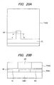
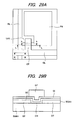
- FIG. 20A is a plan view showing another embodiment of the configuration of a pixel of a display device according to the present invention
- FIG. 20A is a view showing that a second transparent oxide layer TOX2 formed as the upper layer of the two transparent oxide layers formed on the surface of a substrate SUB1 is formed on the entire region of the pixel region, and a gate signal line GL and a gate electrode GT are formed in a part of the second transparent oxide layer TOX2.
- FIG. 20B is a cross-sectional view taken along the line b-b in FIG. 20A .
- a first transparent oxide layer TOX1 formed as the lower layer of the two transparent oxide layers TOX1 and TOX2 formed on the surface of a substrate SUB1 is formed on the entire region of the pixel region, and a source signal line SL, a thin film transistor TFT connected to the source signal line SL, and a pixel electrode PX connected to the thin film transistor TFT are formed in a part of the first transparent oxide layer TOX1.
- the region other than the source signal line SL, the thin film transistor TFT and the pixel electrode PX is a region (insulating region) where modification in terms of crystallinity (or impurity doping) is not performed. Accordingly, the first transparent oxide layer TOX1 is configured to be a flat layer having no difference in level.
- the second transparent oxide layer TOX2 is formed on the upper surface of the first transparent oxide layer TOX1 via an insulating film GI across the entire region of the pixel region, and a gate signal line GL and a gate electrode GT connected to the gate signal line GL are formed in a part of the second transparent oxide layer TOX2. More specifically, in this second transparent oxide layer TOX2, the modification in terms of crystallinity (or impurity doping) is not performed in the region other than the gate signal line GL and the gate electrode GT, and therefore, a sufficient transparency is maintained in this region. Therefore, the second transparent oxide layer TOX2 is also configured to be a flat layer having no difference in level.
- the source signal line SL, the gate signal line GL, the thin film transistor TFT, and the pixel electrode PX can be formed from a sequential stacked body of the first transparent oxide layer TOX1, the insulating film GI, and the second transparent oxide layer TOX2 formed on the entire region of the pixel region. Therefore, the display device can be configured to have a surface having no difference in level.
- FIG. 21 is a plan view showing another embodiment of the configuration of a pixel of the display device according to the present invention, and FIG. 21 corresponds to FIG. 20A .
- FIG. 21 shows a configuration in which the counter electrode CT and the common signal line CL connected to the counter electrode CT are provided for the substrate SUB1.
- the counter electrode CT and the common signal line CL are formed in a part of the second transparent oxide layer TOX2 shown in FIG. 20A .
- the counter electrode CT and the common signal line CL are formed together with the gate signal line GL and the gate electrode GT.
- the difference in level on the surface of the substrate SUB1 can be avoided.
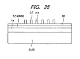
- FIG. 22 is a plan view showing an embodiment of each pixel disposed in an array on the surface of the substrate SUB1, and FIG. 22 corresponds to FIG. 1 .
- FIG. 22 The configuration of FIG. 22 is different from that of FIG. 1 in the thin film transistor TFT, and a semiconductor layer SC thereof is formed so as to be protruded from both sides of the gate electrode GT.
- the semiconductor layer SC is formed separately from the first transparent oxide layer TOX1 constituting the source signal line SL, the pixel electrode PX and others.
- FIG. 23A is an enlarged view of one pixel extracted from the pixels of FIG. 22
- FIG. 23B is a cross-sectional view taken along the line b-b in FIG. 23A .
- a source region portion ST and a drain region portion DT of the thin film transistor TFT are physically separated and disposed on the surface of the substrate SUB1.
- the source region portion ST is formed as an extended portion of the source signal line SL and the drain region portion DT is formed as an extended portion of the pixel electrode PX, and both of them are formed from, for example, the first transparent oxide layer TOX1 constituted of a transparent oxide film made of ZnO, ITO or the like doped with an impurity.
- the first transparent oxide layer TOX1 is formed in each of the forming regions of a source signal line SL, a source region portion ST of the thin film transistor TFT serving as the extended portion of the source signal line SL, a pixel electrode PX, and a drain region portion of the thin film transistor TFT serving as the extended portion of the pixel electrode PX, and moreover, it is configured to have a pattern with a notched portion formed in the channel region portion of the thin film transistor TFT.
- the semiconductor layer SC is disposed between the source region portion ST and the drain region portion DT so as to be overlapped on the source region portion ST at one end and overlapped on the drain region portion DT at the other end.
- the semiconductor layer SC between the source region portion ST and the drain region portion DT functions as a channel region portion CH of the thin film transistor TFT.
- An insulating film GI is formed over the surface of the substrate SUB1 so as to cover the source signal line SL, the source region portion ST, the semiconductor layer SC, the drain region portion DT, the pixel electrode PX and others, and the gate electrode GT is formed on the upper surface of this insulating film GI so as to be overlapped on the channel region of the semiconductor layer SC.
- the gate electrode GT is configured as an extended portion of the gate signal line GL.
- FIG. 25A to FIG. 25H are process drawings showing an embodiment of a manufacturing method of the display device.
- FIG. 25A to FIG. 25H show the process drawings in one pixel of a liquid crystal display region
- the process drawings on the left side of FIG. 25A to FIG. 25H correspond to the cross sections of the line L-L in the pixel shown in FIG. 24
- the process drawings on the right side of FIG. 25A to FIG. 25H correspond to the cross sections of the line R-R in the pixel shown in FIG. 24
- the pixel shown in FIG. 24 is the same as that shown in FIG. 23A .
- the substrate SUB1 is prepared, and the first transparent oxide layer TOX1 made of, for example, ZnO doped with an impurity is formed on the surface of the substrate SUB1.
- a first photoresist film PRT1 is formed over the surface of the substrate SUB1, and the first photoresist film PRT1 is patterned, thereby forming the first photoresist film PRT1 left in the forming regions of the source signal line SL, the source region portion ST of the thin film transistor TFT serving as an extended portion of the source signal line SL, the pixel electrode PX, and the drain region portion DT of the thin film transistor TFT serving as an extended portion of this pixel electrode PX.
- the first transparent oxide layer TOX1 exposed from the mask is selectively etched.
- the source signal line SL, the source region portion ST of the thin film transistor TFT, the pixel electrode PX, and the drain region portion DT of the thin film transistor TFT are formed.
- the first photoresist film PRT1 is removed.
- the second photoresist PRT2 is formed over the surface of the substrate SUB1, and the second photoresist film PRT2 is patterned, thereby forming the photoresist film PRT2 having an opening which exposes a space portion between the source region portion ST and the drain region portion DT, an end portion of the source region portion ST on the space portion side, and an end portion of the drain region portion DT on the space portion side.
- the second transparent oxide layer TOX2 made of, for example, ZnO doped with an intrinsic or low-concentration impurity is formed over the surface of the substrate SUB1.
- the second transparent oxide layer TOX2 disposed so as to be overlapped on the source region portion ST at one end and overlapped on the drain region portion DT at the other end is selectively formed. This is the formation by a so-called lift off method.
- the second transparent oxide layer TOX2 is configured as a semiconductor layer SC of the thin film transistor TFT.
- an insulating film GI constituted of, for example, an SiO 2 film and a third transparent oxide layer TOX3 constituted of, for example, an ITO film are sequentially formed over the surface of the substrate SUB1.
- the insulating film GI functions as a gate insulating film of the thin film transistor TFT and an interlayer insulating film of the later-described gate signal line GL for the source signal line SL.
- the gate insulating film of the thin film transistor TFT may be formed by forming an insulating film to be stacked on the semiconductor layer of the thin film transistor TFT in the process 4.
- a third photoresist film PRT3 is formed over the surface of the substrate SUB1, and the third photoresist film PRT3 is patterned, thereby leaving the third photoresist film PRT3 in the forming regions of the gate electrode GT and the gate signal line GL connected to the gate electrode GT.
- the third transparent oxide layer TOX3 exposed from the mask is selectively etched.
- the gate electrode GT and the gate signal line GL are formed.
- the third photoresist film PRT3 is removed.
- FIG. 26A is a plan view showing another embodiment of the pixel of a display device according to the present invention, and FIG. 26A corresponds to FIG. 23A . Also, the cross-sectional view taken along the line b-b in FIG. 26A is shown in FIG. 26B .
- FIG. 26A and FIG. 26B The configuration of FIG. 26A and FIG. 26B is different from that of FIG. 23A and FIG. 23B in the semiconductor layer SC functioning as a channel region portion of the thin film transistor TFT, and the semiconductor layer SC is formed so as to be stacked not only on the channel region portion of the thin film transistor TFT but also on the source signal line SL, the source region portion ST and the drain region portion DT of the thin film transistor TFT, and the pixel electrode PX.
- FIG. 27A to FIG. 27I are process drawings showing an embodiment of the manufacturing method of the display device.
- FIG. 27A to FIG. 27I show the process drawings in one pixel of a liquid crystal display region
- the process drawings on the left side of FIG. 27A to FIG. 27I correspond to the cross sections of the line L-L in the pixel shown in FIG. 26A
- the process drawings on the right side of FIG. 27A to FIG. 27I correspond to the cross sections of the line R-R in the pixel shown in FIG. 26A .
- the substrate SUB1 is prepared, and the first transparent oxide layer TOX1 made of, for example, ZnO doped with an impurity is formed on the surface of the substrate SUB1.
- a first photoresist film PRT1 is formed over the surface of the substrate SUB1, and the first photoresist film PRT1 is patterned, thereby leaving the first photoresist film PRT1 having an opening in the region where the semiconductor layer SC of the thin film transistor TFT is to be formed.
- the first transparent oxide layer TOX1 exposed from the mask is selectively etched.
- the first photoresist film PRT1 is removed.
- the second transparent oxide layer TOX2 made of, for example, ZnO doped with an intrinsic or low-concentration impurity is formed over the surface of the substrate SUB1.
- the second transparent oxide layer TOX2 functions as the semiconductor layer SC of the thin film transistor TFT in the portion where the first transparent oxide layer TOX1 has been selectively etched.
- the second photoresist film PRT2 is formed over the surface of the substrate SUB1, and the second photoresist film PRT2 is patterned, thereby leaving the second photoresist film PRT2 in the forming regions of the source signal line SL, the source region portion ST of the thin film transistor TFT, the channel region portion CH, the drain region portion DT, and the pixel electrode PX.
- the first transparent oxide layer TOX1 exposed from the mask is electively etched.
- the second photoresist film PRT2 is removed.
- the first transparent oxide layer TOX1 constituting the source signal line SL, the source region portion ST of the thin film transistor TFT constituted as the extended portion of the source signal line SL, the pixel electrode PX, and the drain region portion DT of the thin film transistor TFT constituted as the extended portion of the pixel electrode PX is formed on the surface of the substrate SUB1, and the second transparent oxide layer TOX2 is formed in the forming region of the semiconductor layer SC of the thin film transistor TFT (portion of an opening of the first transparent oxide layer TOX1) and on the first transparent oxide layer TOX1.
- an insulating film GI constituted of, for example, an SiO 2 film and a third transparent oxide layer TOX3 constituted of, for example, an ITO film are sequentially formed over the surface of the substrate SUB1.
- the insulating film GI functions as a gate insulating film of the thin film transistor TFT and an interlayer insulating film of the later-described gate signal line GL for the source signal line SL.
- a third photoresist film PRT3 is formed over the surface of the substrate SUB1, and the third photoresist film PRT3 is patterned, thereby leaving the third photoresist film PRT3 in the forming regions of the gate electrode GT and the gate signal line GL connected to the gate electrode GT.
- the third transparent oxide layer TOX3 exposed from the mask is selectively etched.
- the gate electrode GT and the gate signal line GL are formed.
- the semiconductor layer SC constituting the channel region portion of the thin film transistor TFT is disposed on the transparent oxide layer constituting the source signal line SL, the source region portion ST and the drain region portion DT of the thin film transistor TFT, and the pixel electrode PX.
- the configuration in which the positional relationship in these layers is reversed is also possible, that is, the configuration may be such that the semiconductor layer SC constituting the channel region portion of the thin film transistor TFT is disposed below the transparent oxide layer constituting the source signal line SL, the source region portion ST and the drain region portion DT of the thin film transistor TFT, and the pixel electrode PX.
- FIG. 28A to FIG. 28D A part of the process in an embodiment of the manufacturing method of the pixel with the configuration as described above is shown in FIG. 28A to FIG. 28D .
- the substrate SUB1 is prepared, and the first transparent oxide layer TOX1 made of, for example, ZnO and the second transparent oxide layer TOX2 made of, for example, ZnO doped with an impurity are sequentially formed on the surface of the substrate SUB1.
- the first transparent oxide layer TOX1 made of, for example, ZnO and the second transparent oxide layer TOX2 made of, for example, ZnO doped with an impurity are sequentially formed on the surface of the substrate SUB1.
- a first photoresist film PRT1 is formed over the surface of the substrate SUB1, and the first photoresist film PRT1 is patterned.
- the first photoresist film PRT 1 is left in the forming regions of the source signal line SL, the source region portion ST of the thin film transistor TFT constituted as an extended portion of the source signal line SL, the channel region portion CH of the thin film transistor TFT, the pixel electrode PX, and the drain region portion DT of the thin film transistor TFT constituted as an extended portion of the pixel electrode PX, and moreover, the first photoresist film PRT1 is formed to have a thickness smaller in a portion corresponding to the forming region of the channel region portion CH of the thin film transistor TFT than that of other portions.
- the second transparent oxide layer TOX2 and its underlying first transparent oxide layer TOX1 exposed from the mask are selectively etched.
- the surface of the first photoresist film PRT1 is removed by an appropriate amount toward the bottom surface thereof, so that the surface of the second transparent oxide layer TOX2 in the forming region of the channel region portion of the thin film transistor TFT is exposed, and the first photoresist PRT1 is left in other portions.
- the second transparent oxide layer TOX2 in the forming region of the channel region portion of the thin film transistor TFT is selectively etched, and the surface of the first transparent oxide layer TOX1 below the second transparent oxide layer TOX2 is exposed.
- the first photoresist PRT1 is removed.
- the subsequent process is completed after performing the processes shown in FIG. 27G to FIG. 27I .
- FIG. 29A is a plan view showing another embodiment of the configuration of a pixel of the display device according to the present invention, and FIG. 29A corresponds to FIG. 26A .
- FIG. 29A and FIG. 29B The configuration of FIG. 29A and FIG. 29B is different from that of FIG. 26A and FIG. 26B in that the second transparent oxide layer TOX2 formed as the semiconductor layer SC of the thin film transistor TFT does not terminate in the vicinity of the channel region portion CH of the thin film transistor TFT, but is formed across the entire region of the pixel region.
- the second transparent oxide layer TOX2 formed as the semiconductor layer SC of the thin film transistor TFT does not terminate in the vicinity of the channel region portion CH of the thin film transistor TFT, but is formed across the entire region of the pixel region.
- the first transparent oxide layer TOX1 is formed in each of the forming regions of the source signal line SL, the source region portion ST of the thin film transistor TFT constituted as the extended portion of the source signal line SL, the pixel electrode PX, and the drain region portion DT of the thin film transistor TFT constituted as the extended portion of the pixel electrode PX.
- FIG. 30A to FIG. 30F are process drawings showing an embodiment of the manufacturing method of the above-described display device.
- FIG. 30A to FIG. 30F show the process drawings in the pixel
- the process drawings shown on the left side of FIG. 30A to FIG. 30F correspond to the cross section of the line L-L in the pixel shown in FIG. 29A
- the process drawings on the right side of FIG. 30A to FIG. 30F correspond to the cross sections of the line R-R in the pixel shown in FIG. 29A .
- the substrate SUB1 is prepared, and the first transparent oxide layer TOX1 made of, for example, ZnO doped with an impurity is formed on the surface of the substrate SUB1.
- a first photoresist film PRT1 is formed over the surface of the substrate SUB1, and the first photoresist film PRT1 is patterned, thereby leaving the first photoresist film PRT 1 in the forming regions of the source signal line SL, the source region portion ST of the thin film transistor TFT constituted as an extended portion of the source signal line SL, the pixel electrode PX, and the drain region portion DT of the thin film transistor TFT constituted as an extended portion of the pixel electrode PX.
- the first transparent oxide layer TOX1 exposed from the mask is selectively etched.
- the first photoresist film PRT1 is removed.
- the semiconductor layer SC made of, for example, ZnO doped with an intrinsic or low-concentration impurity and the insulating film GI constituted of, for example, an SiO 2 film are sequentially formed over the surface of the substrate SUB1.
- the semiconductor layer SC functions as a semiconductor layer in the forming region of the thin film transistor TFT
- the insulating film GI functions as a gate insulating film of the thin film transistor TFT and an interlayer insulating film of the later-described gate signal line GL for the source signal line SL.
- the second transparent oxide layer TOX2 made of, for example, ITO is formed over the surface of the substrate SUB1.
- the second photoresist film PRT2 is formed over the surface of the substrate SUB1, and the second photoresist film PRT2 is patterned, thereby leaving the second photoresist film PRT2 in the forming regions of the gate electrode GT and the gate signal line GL connected to the gate electrode GT.
- the second transparent oxide layer TOX2 exposed from the mask is electively etched.
- the gate electrode GT and the gate signal line GL are formed.
- the second photoresist film PRT2 is removed.
- FIG. 31A is a plan view showing another embodiment of the configuration of a pixel of a display device according to the present invention, and FIG. 31A corresponds to FIG. 23A . Also, FIG. 31B is a cross-sectional view taken along the line b-b in FIG. 31A .
- FIG. 31A and FIG. 31B The configuration of FIG. 31A and FIG. 31B is different from that of FIG. 23A and FIG. 23B in that a new source signal line SL' is provided to be overlapped with a source signal line SL formed from a transparent oxide layer.
- the source signal line SL' is constituted of, for example, a metal layer and formed on the surface of a substrate SUB1.
- FIG. 23A and FIG. 23B the configuration shown in FIG. 23A and FIG. 23B is formed over the surface of the substrate SUB1 on which the source signal line SL' is formed, and the source signal line SL is overlapped on the source signal line SL'.
- the source signal line of a multilayered structure including the metal layer can be obtained, so that the electric resistance of the source signal line can be significantly reduced.
- FIG. 32A and FIG. 32B are cross-sectional views taken along the line IIIXII-IIIXII in FIG. 31A .
- the substrate SUB1 is prepared, and a metal layer MT is formed on the entire region of the surface of the substrate SUB1, and a photoresist film PRT is formed on the surface of the metal layer MT. Then, the photoresist film PRT is patterned, thereby leaving the photoresist film PRT in the forming region of the source signal line SL'.
- the metal layer MT exposed from the mask is selectively etched.
- the photoresist film PRT is removed, and the transparent oxide layer TOX made of, for example, ZnO doped with an impurity is formed over the surface of the substrate SUB1.
- the formation of the transparent oxide layer TOX corresponds to the process of FIG. 25A , and thereafter, by performing the processes of FIG. 25B to FIG. 25H , the pixel shown in FIG. 31 can be completed.
- the source signal line SL of the transparent oxide layer is stacked on the almost entire region in the longitudinal direction of the source signal line SL' constituted of a metal layer.
- the source signal line SL of the transparent oxide layer is not always required to be formed across the almost entire length of the source signal line SL', and for example, it may be formed only in the vicinity of the thin film transistor TFT. This is because the electric resistance of the source signal line can be reduced even in this configuration.
- the source signal line SL' constituted of a metal layer is formed below the source signal line SL of the transparent oxide layer.
- the source signal line SL' constituted of a metal layer can be formed on the source signal line SL of the transparent oxide layer.
- FIG. 33A and FIG. 33B are configuration diagrams showing an embodiment of the case where the source signal line SL' is formed on the source signal line SL, and FIG. 33A and FIG. 33 correspond to FIG. 31A and FIG. 31B .
- FIG. 34A is a plan view showing another embodiment of the configuration of a pixel of a display device according to the present invention, and FIG. 34A corresponds to FIG. 23A . Also, FIG. 34B is a cross-sectional view taken along the line b-b in the FIG. 34A .
- FIG. 34A The configuration of FIG. 34A is different from that of FIG. 23A in that the counter electrode CT generating an electric field with the pixel electrode PX and the common signal line CL supplying the signal having a voltage serving as a reference for a video signal to the counter electrode CT are provided over the surface of the substrate SUB1.
- the counter electrode CT is overlapped on the pixel electrode PX via the insulating film GI, and a number of counter electrodes CT disposed in parallel to one another form an electrode group and are integrally formed with the common signal line CL.
- the counter electrode CT and the common signal line CL are formed in the same layer as, for example, the gate signal line GL.
- the counter electrode CT and the common signal line CL may be formed of a metal layer.
- the counter electrode CT and the common signal line CL may be selectively formed together with the gate signal line GL (gate electrode GT) in the transparent oxide layer formed across the entire region of the pixel.
- a transparent oxide layer TOX (ND) not doped with an impurity may be interposed between the insulating film GI and the pixel electrode PX.
- the transparent oxide layer TOX (ND) functions as, for example, a semiconductor layer SC in the forming region of the thin film transistor TFT, and it is not selectively removed and is formed over the region of the pixel.
- FIG. 36 shows that the pixel with the above-described configuration (not shown) is formed on the substrate SUB 1, and at the same time, the supply of the scanning signal to each gate signal line GL is performed by a gate signal drive circuit V mounted on the substrate SUB1, and the supply of a video signal to each source signal line SL is performed by a source signal drive circuit He mounted on the substrate SUB1.
- the gate signal line GL may be formed of a single film of molybdenum, chromium, tungsten, aluminum, copper, titanium, nickel, tantalum, silver, zinc, or other metal, an alloy film made of these metals, a stacked film of these metals, or a stacked film of these films and a transparent oxide layer made of ITO, ZnO or the like.
- the metal layer may be formed of a single film of molybdenum, chromium, tungsten, aluminum, copper, titanium, nickel, tantalum, silver, zinc or other metal, a stacked film of these metals, or an alloy film of these metals.
- the counter electrode CT or the common signal line CL supplying the signal to the counter electrode CT may be formed of a single film of molybdenum, chromium, tungsten, aluminum, copper, titanium, nickel, tantalum, silver, zinc or other metal, a stacked film of these metals, an alloy film of these metals or a stacked film of these films and a transparent oxide layer of ITO, ZnO, or the like.
- the substrate SUB may be formed as a flexible substrate made of, for example, synthetic resin or stainless instead of the general glass substrate. This is because, since the materials that can be formed at a low temperature are used, synthetic resin can be used as the material of the substrate SUB1.
- the above-described display device and the manufacturing method thereof can be applied not only to each liquid crystal display device of a transmission type, a reflection type, a half-transmission type, an IPS type, and an IPS-Pro type but also to other display devices such as an organic EL display device. This is because the display devices provided with a thin film transistor for each pixel and performing an active matrix drive have the same problem to be solved.
Landscapes
- Engineering & Computer Science (AREA)
- Power Engineering (AREA)
- Physics & Mathematics (AREA)
- Microelectronics & Electronic Packaging (AREA)
- General Physics & Mathematics (AREA)
- Condensed Matter Physics & Semiconductors (AREA)
- Computer Hardware Design (AREA)
- Chemical & Material Sciences (AREA)
- Crystallography & Structural Chemistry (AREA)
- Nonlinear Science (AREA)
- Ceramic Engineering (AREA)
- Mathematical Physics (AREA)
- Optics & Photonics (AREA)
- Liquid Crystal (AREA)
- Manufacturing & Machinery (AREA)
- Thin Film Transistor (AREA)
- Devices For Indicating Variable Information By Combining Individual Elements (AREA)
- Electroluminescent Light Sources (AREA)
Claims (9)
- Dispositif d'affichage, comprenant
un substrat (SUB1), sur lequel une couche d'oxyde transparente (TOX1), un film isolant (G) et une couche conductrice sont empilés dans cet ordre sur une région de pixels,
dans lequel la couche conductrice possède une partie d'électrode de grille (GT) d'un transistor à couche mince (TFT), et
dans lequel une région de la couche d'oxyde transparente (TOX1), à l'exception d'au moins une partie de région de canal située directement en dessous de l'électrode de grille, est convertie en une région électriquement conductrice constituant une électrode de pixel (PX) et une partie de région de drain (DT) du transistor à couche mince relié à l'électrode de pixel (PX),
caractérisé en ce que
une ligne de signaux de source (SL) et une partie de région de source du transistor à couche mince (TFT) reliée à la ligne de signaux de source sont également formées à partir de la région conductrice, et
le film isolant (GI) est formé de manière à recouvrir une surface supérieure de la couche d'oxyde transparente (TOX1). - Le dispositif d'affichage selon la revendication 1,
dans lequel la couche d'oxyde transparente semi-conductrice (TOX1) possède une partie de la région de canal (CH) du transistor à couche mince (TFT) située directement en dessous de l'électrode de grille (GT), et
dans lequel la concentration de porteurs dans la ligne de signaux de source (SL), la partie de région de source (ST), la partie de région de drain (DT) et l'électrode de pixel (PX) sont supérieures à une concentration de porteurs dans la partie de région de canal (CH). - Le dispositif d'affichage selon la revendication 1, comprenant en outre
une couche semi-conductrice (SC),
dans lequel la partie de région de source (ST) et la partie de région de drain (DT) sont formées avec un espace entre les deux, et
la couche semi-conductrice (SC) est disposée dans l'espace entre la partie de région de source (ST) et la partie de région de drain (DT) de telle sorte que la couche semi-conductrice (SC) a une extrémité sur la partie de région de source (ST) et une autre extrémité sur la partie de région de drain (DT), pour fonctionner comme une partie de région de canal (CH) du transistor à couche mince (TFT) située directement en dessous de l'électrode de grille (GT), et
dans lequel la concentration de porteurs de la ligne de signaux de source (SL), la partie de région de source (ST), la partie de région de drain (DT) et l'électrode de pixel (PX) étant supérieure à une concentration de porteurs de la couche semi-conductrice (SC). - Le dispositif d'affichage selon l'une quelconque des revendications 1 à 3,
dans lequel la couche conductrice inclut des parties pour une contre-électrode (CT) se chevauchant sur l'électrode de pixel (PX) et disposées parallèlement sur le film isolant (GI) et une ligne de signaux commune (CL) fournissant un signal à chaque électrode de la contre-électrode (CT). - Le dispositif d'affichage selon l'une quelconque des revendications 1 à 3,
dans lequel le film isolant (GI) est formé dans l'ensemble de la région de pixels. - Le dispositif d'affichage selon l'une quelconque des revendications 1 à 3,
dans lequel la couche conductrice est constituée d'une couche métallique (TM). - Le dispositif d'affichage selon l'une quelconque des revendications 1 à 3,
dans lequel la couche conductrice est constituée d'un film ITO. - Le dispositif d'affichage selon l'une quelconque des revendications 1 à 3, comprenant en outre une seconde couche d'oxyde transparente semi-conductrice (TOX2) formée dans l'ensemble de la région de pixels, la seconde couche d'oxyde transparente semi-conductrice ayant une partie de cristallinité modifiée pour la couche conductrice.
- Le dispositif d'affichage selon la revendication 2 ou 3,
dans lequel les parties de région LDD avec une concentration de porteurs inférieure à celle de la partie de région de source (ST) et de la partie de région de drain (DT) sont formées dans la couche d'oxyde transparente semi-conductrice (TOX1) entre la partie de région de canal (CH) située directement en dessous de l'électrode de grille (GT) et la partie de région de source (ST) et entre la partie de région de canal (CH) et la partie de région de drain (DT), respectivement.
Applications Claiming Priority (1)
| Application Number | Priority Date | Filing Date | Title |
|---|---|---|---|
| JP2007006570A JP5111867B2 (ja) | 2007-01-16 | 2007-01-16 | 表示装置 |
Publications (3)
| Publication Number | Publication Date |
|---|---|
| EP1947695A2 EP1947695A2 (fr) | 2008-07-23 |
| EP1947695A3 EP1947695A3 (fr) | 2010-05-19 |
| EP1947695B1 true EP1947695B1 (fr) | 2011-07-27 |
Family
ID=39301275
Family Applications (1)
| Application Number | Title | Priority Date | Filing Date |
|---|---|---|---|
| EP07025121A Active EP1947695B1 (fr) | 2007-01-16 | 2007-12-27 | Dispositif d'affichage |
Country Status (7)
| Country | Link |
|---|---|
| US (4) | US8242505B2 (fr) |
| EP (1) | EP1947695B1 (fr) |
| JP (1) | JP5111867B2 (fr) |
| KR (1) | KR101454919B1 (fr) |
| CN (1) | CN101226311B (fr) |
| AT (1) | ATE518253T1 (fr) |
| TW (1) | TW200839401A (fr) |
Families Citing this family (32)
| Publication number | Priority date | Publication date | Assignee | Title |
|---|---|---|---|---|
| JP5111867B2 (ja) * | 2007-01-16 | 2013-01-09 | 株式会社ジャパンディスプレイイースト | 表示装置 |
| JP2010108957A (ja) * | 2008-10-28 | 2010-05-13 | Hitachi Displays Ltd | 表示装置およびその製造方法 |
| KR101510900B1 (ko) * | 2008-12-04 | 2015-04-10 | 엘지디스플레이 주식회사 | 산화물 반도체층을 이용한 액정표시장치용 어레이 기판의 제조방법 |
| JP4844627B2 (ja) * | 2008-12-24 | 2011-12-28 | ソニー株式会社 | 薄膜トランジスタの製造方法および表示装置の製造方法 |
| KR101746198B1 (ko) | 2009-09-04 | 2017-06-12 | 가부시키가이샤 한도오따이 에네루기 켄큐쇼 | 표시장치 및 전자기기 |
| KR102049472B1 (ko) * | 2010-02-19 | 2019-11-27 | 가부시키가이샤 한도오따이 에네루기 켄큐쇼 | 반도체 장치 |
| CN102148196B (zh) * | 2010-04-26 | 2013-07-10 | 北京京东方光电科技有限公司 | Tft-lcd阵列基板及其制造方法 |
| WO2011142371A1 (fr) * | 2010-05-14 | 2011-11-17 | Semiconductor Energy Laboratory Co., Ltd. | Dispositif à semi-conducteurs |
| WO2012073942A1 (fr) * | 2010-12-01 | 2012-06-07 | シャープ株式会社 | Dispositif à semi-conducteurs et son procédé de production |
| JP5743064B2 (ja) * | 2011-02-17 | 2015-07-01 | 株式会社Joled | 薄膜トランジスタおよびその製造方法、並びに表示装置 |
| FR2981090B1 (fr) * | 2011-10-10 | 2014-03-14 | Commissariat Energie Atomique | Procede de preparation d'oxyde de zinc zno de type p ou de znmgo de type p. |
| CN102629585B (zh) | 2011-11-17 | 2014-07-23 | 京东方科技集团股份有限公司 | 一种显示装置、薄膜晶体管、阵列基板及其制造方法 |
| US9099560B2 (en) * | 2012-01-20 | 2015-08-04 | Semiconductor Energy Laboratory Co., Ltd. | Semiconductor device and manufacturing method thereof |
| JP6148024B2 (ja) * | 2012-02-09 | 2017-06-14 | 株式会社半導体エネルギー研究所 | 半導体装置 |
| CN102629590B (zh) * | 2012-02-23 | 2014-10-22 | 京东方科技集团股份有限公司 | 一种薄膜晶体管阵列基板及其制作方法 |
| TWI477867B (zh) * | 2012-07-16 | 2015-03-21 | E Ink Holdings Inc | 畫素結構及其製造方法 |
| KR102101863B1 (ko) * | 2013-01-07 | 2020-04-21 | 삼성디스플레이 주식회사 | 박막 트랜지스터, 이의 제조 방법 및 이를 구비하는 표시 장치 |
| JP2014132621A (ja) * | 2013-01-07 | 2014-07-17 | Nippon Hoso Kyokai <Nhk> | 薄膜デバイスの製造方法 |
| KR102040812B1 (ko) * | 2013-02-12 | 2019-11-06 | 삼성디스플레이 주식회사 | 액정 표시 장치 |
| KR102054000B1 (ko) * | 2013-09-11 | 2019-12-10 | 삼성디스플레이 주식회사 | 박막 트랜지스터 표시판, 액정 표시 장치 및 박막 트랜지스터 표시판의 제조방법 |
| KR102345617B1 (ko) * | 2014-01-13 | 2022-01-03 | 삼성디스플레이 주식회사 | 표시패널 |
| CN103746013B (zh) * | 2014-01-20 | 2016-03-30 | 瑞德兴阳新能源技术有限公司 | 一种石墨烯太阳能电池及其制备方法 |
| CN103746014B (zh) * | 2014-01-20 | 2016-03-30 | 瑞德兴阳新能源技术有限公司 | 一种ito栅线太阳能电池及其制备方法 |
| WO2016093122A1 (fr) * | 2014-12-09 | 2016-06-16 | シャープ株式会社 | Procédé de fabrication d'un substrat de panneau d'affichage |
| US9837547B2 (en) | 2015-05-22 | 2017-12-05 | Semiconductor Energy Laboratory Co., Ltd. | Semiconductor device comprising oxide conductor and display device including the semiconductor device |
| WO2016204227A1 (fr) * | 2015-06-17 | 2016-12-22 | 富士電機株式会社 | Dispositif à semi-conducteur et procédé de fabrication de dispositif à semi-conducteur |
| EP3136446A1 (fr) * | 2015-08-28 | 2017-03-01 | Nederlandse Organisatie voor toegepast- natuurwetenschappelijk onderzoek TNO | Dispositif tft et procédé de fabrication |
| JP2017075982A (ja) * | 2015-10-13 | 2017-04-20 | 株式会社ジャパンディスプレイ | 表示装置 |
| WO2018100466A1 (fr) * | 2016-11-30 | 2018-06-07 | Semiconductor Energy Laboratory Co., Ltd. | Dispositif d'affichage, module d'affichage et dispositif électronique |
| CN108039353B (zh) * | 2017-12-26 | 2020-07-21 | 深圳市华星光电技术有限公司 | 阵列基板及其制备方法、显示装置 |
| CN110224003B (zh) * | 2018-03-01 | 2023-06-09 | 天马日本株式会社 | 显示装置 |
| JP6753986B2 (ja) * | 2019-07-04 | 2020-09-09 | 株式会社半導体エネルギー研究所 | 半導体装置 |
Family Cites Families (18)
| Publication number | Priority date | Publication date | Assignee | Title |
|---|---|---|---|---|
| JPS62145247A (ja) | 1985-12-19 | 1987-06-29 | Nec Corp | フオトマスク |
| JP2794678B2 (ja) * | 1991-08-26 | 1998-09-10 | 株式会社 半導体エネルギー研究所 | 絶縁ゲイト型半導体装置およびその作製方法 |
| JP3259119B2 (ja) | 1994-06-28 | 2002-02-25 | 富士通株式会社 | 配線パターン基板及び薄膜トランジスタマトリクス基板とその製造方法 |
| JPH09269503A (ja) * | 1996-03-29 | 1997-10-14 | Toshiba Corp | 液晶表示装置 |
| JPH09318975A (ja) * | 1996-05-30 | 1997-12-12 | Nec Corp | 薄膜電界効果型トランジスタ素子アレイおよびその製造 方法 |
| JP2001076885A (ja) * | 1999-09-02 | 2001-03-23 | Auto Network Gijutsu Kenkyusho:Kk | 有機el表示デバイスにおける透明配線の抵抗値調節方法 |
| JP3617458B2 (ja) | 2000-02-18 | 2005-02-02 | セイコーエプソン株式会社 | 表示装置用基板、液晶装置及び電子機器 |
| JP2003050405A (ja) * | 2000-11-15 | 2003-02-21 | Matsushita Electric Ind Co Ltd | 薄膜トランジスタアレイ、その製造方法およびそれを用いた表示パネル |
| KR20020038482A (ko) * | 2000-11-15 | 2002-05-23 | 모리시타 요이찌 | 박막 트랜지스터 어레이, 그 제조방법 및 그것을 이용한표시패널 |
| JP2002319682A (ja) * | 2002-01-04 | 2002-10-31 | Japan Science & Technology Corp | トランジスタ及び半導体装置 |
| JP4141309B2 (ja) * | 2003-04-15 | 2008-08-27 | シャープ株式会社 | 半導体装置およびその製造方法 |
| US6960497B2 (en) | 2003-06-25 | 2005-11-01 | Chunghwa Picture Tubes, Ltd. | Method for forming pi-type assistant electrode |
| JP4404881B2 (ja) * | 2006-08-09 | 2010-01-27 | 日本電気株式会社 | 薄膜トランジスタアレイ、その製造方法及び液晶表示装置 |
| TWI374544B (en) * | 2006-11-13 | 2012-10-11 | Au Optronics Corp | Thin film transistor array substrates and fbricating method thereof |
| JP5111867B2 (ja) * | 2007-01-16 | 2013-01-09 | 株式会社ジャパンディスプレイイースト | 表示装置 |
| EP3236504A1 (fr) * | 2009-06-30 | 2017-10-25 | Semiconductor Energy Laboratory Co., Ltd. | Procédé de fabrication d'un dispositif semi-conducteur |
| KR20190000365A (ko) * | 2010-02-26 | 2019-01-02 | 가부시키가이샤 한도오따이 에네루기 켄큐쇼 | 반도체 장치를 제작하기 위한 방법 |
| KR101854421B1 (ko) * | 2010-04-23 | 2018-05-03 | 가부시키가이샤 한도오따이 에네루기 켄큐쇼 | 반도체 장치의 제작 방법 |
-
2007
- 2007-01-16 JP JP2007006570A patent/JP5111867B2/ja active Active
- 2007-11-12 TW TW096142729A patent/TW200839401A/zh unknown
- 2007-11-23 KR KR1020070120116A patent/KR101454919B1/ko active IP Right Grant
- 2007-12-26 US US12/003,462 patent/US8242505B2/en active Active
- 2007-12-27 CN CN2007103004216A patent/CN101226311B/zh active Active
- 2007-12-27 EP EP07025121A patent/EP1947695B1/fr active Active
- 2007-12-27 AT AT07025121T patent/ATE518253T1/de not_active IP Right Cessation
-
2012
- 2012-06-29 US US13/537,462 patent/US8629451B2/en active Active
-
2013
- 2013-12-13 US US14/106,287 patent/US8802511B2/en active Active
-
2014
- 2014-05-15 US US14/278,358 patent/US10068932B2/en active Active
Also Published As
| Publication number | Publication date |
|---|---|
| US20140106490A1 (en) | 2014-04-17 |
| JP2008175842A (ja) | 2008-07-31 |
| EP1947695A3 (fr) | 2010-05-19 |
| CN101226311A (zh) | 2008-07-23 |
| TWI370312B (fr) | 2012-08-11 |
| TW200839401A (en) | 2008-10-01 |
| US8802511B2 (en) | 2014-08-12 |
| US10068932B2 (en) | 2018-09-04 |
| CN101226311B (zh) | 2012-12-12 |
| US8629451B2 (en) | 2014-01-14 |
| KR101454919B1 (ko) | 2014-10-27 |
| US20140248748A1 (en) | 2014-09-04 |
| KR20080067562A (ko) | 2008-07-21 |
| US20080169469A1 (en) | 2008-07-17 |
| EP1947695A2 (fr) | 2008-07-23 |
| US20120261668A1 (en) | 2012-10-18 |
| ATE518253T1 (de) | 2011-08-15 |
| JP5111867B2 (ja) | 2013-01-09 |
| US8242505B2 (en) | 2012-08-14 |
Similar Documents
| Publication | Publication Date | Title |
|---|---|---|
| EP1947695B1 (fr) | Dispositif d'affichage | |
| US7737517B2 (en) | Display device | |
| WO2017065199A1 (fr) | Dispositif à semi-conducteur et son procédé de fabrication | |
| EP3621120B1 (fr) | Transistor à couches minces et son procédé de préparation, substrat de réseau et son procédé de préparation | |
| WO2013137045A1 (fr) | Dispositif à semi-conducteur et son procédé de fabrication | |
| US20110263053A1 (en) | Method for manufacturing pixel structure | |
| JP2005079283A (ja) | 薄膜半導体装置及びその製造方法、電気光学装置、並びに電子機器 | |
| KR101059024B1 (ko) | 표시 장치 | |
| US20080197357A1 (en) | Display panel and manufacturing method | |
| JP2019169606A (ja) | アクティブマトリクス基板およびその製造方法 | |
| CN107799603B (zh) | 薄膜晶体管阵列面板及相关制造方法 | |
| US20050082537A1 (en) | Semiconductor device and method for manufacturing the same | |
| US20060065894A1 (en) | Thin film transistor array panel and manufacturing method thereof | |
| WO2009096148A1 (fr) | Dispositif à semi-conducteur et son procédé de fabrication | |
| US20110193168A1 (en) | Semiconductor device and method for manufacturing same | |
| WO2013191044A1 (fr) | Dispositif semi-conducteur et son procédé de fabrication | |
| JP7437359B2 (ja) | アクティブマトリクス基板およびその製造方法 | |
| KR20060023697A (ko) | 박막트랜지스터 표시판 및 그 제조 방법 | |
| KR20060018136A (ko) | 박막 트랜지스터 기판 및 그 제조방법 | |
| KR20060040327A (ko) | 박막 트랜지스터 표시판 및 그 제조 방법 | |
| KR20060039632A (ko) | 박막 트랜지스터 및 박막 트랜지스터 표시판의 제조 방법 | |
| KR20060070366A (ko) | 박막 트랜지스터 및 박막 트랜지스터 표시판의 제조 방법 | |
| KR20060047022A (ko) | 박막 트랜지스터 표시판의 제조 방법 | |
| KR20060041020A (ko) | 박막 트랜지스터 및 박막 트랜지스터 표시판의 제조방법과 이를 통하여 제조한 박막 트랜지스터 표시판 | |
| KR20060070331A (ko) | 박막 트랜지스터 표시판의 제조 방법 |
Legal Events
| Date | Code | Title | Description |
|---|---|---|---|
| PUAI | Public reference made under article 153(3) epc to a published international application that has entered the european phase |
Free format text: ORIGINAL CODE: 0009012 |
|
| AK | Designated contracting states |
Kind code of ref document: A2 Designated state(s): AT BE BG CH CY CZ DE DK EE ES FI FR GB GR HU IE IS IT LI LT LU LV MC MT NL PL PT RO SE SI SK TR |
|
| AX | Request for extension of the european patent |
Extension state: AL BA HR MK RS |
|
| PUAL | Search report despatched |
Free format text: ORIGINAL CODE: 0009013 |
|
| AK | Designated contracting states |
Kind code of ref document: A3 Designated state(s): AT BE BG CH CY CZ DE DK EE ES FI FR GB GR HU IE IS IT LI LT LU LV MC MT NL PL PT RO SE SI SK TR |
|
| AX | Request for extension of the european patent |
Extension state: AL BA HR MK RS |
|
| RIC1 | Information provided on ipc code assigned before grant |
Ipc: H01L 27/12 20060101ALI20100412BHEP Ipc: H01L 29/786 20060101AFI20100412BHEP Ipc: H01L 21/77 20060101ALI20100412BHEP |
|
| 17P | Request for examination filed |
Effective date: 20101119 |
|
| AKX | Designation fees paid |
Designated state(s): AT BE BG CH CY CZ DE DK EE ES FI FR GB GR HU IE IS IT LI LT LU LV MC MT NL PL PT RO SE SI SK TR |
|
| RIC1 | Information provided on ipc code assigned before grant |
Ipc: H01L 29/786 20060101AFI20101228BHEP Ipc: H01L 27/12 20060101ALI20101228BHEP Ipc: H01L 21/77 20060101ALI20101228BHEP |
|
| GRAP | Despatch of communication of intention to grant a patent |
Free format text: ORIGINAL CODE: EPIDOSNIGR1 |
|
| GRAS | Grant fee paid |
Free format text: ORIGINAL CODE: EPIDOSNIGR3 |
|
| GRAA | (expected) grant |
Free format text: ORIGINAL CODE: 0009210 |
|
| AK | Designated contracting states |
Kind code of ref document: B1 Designated state(s): AT BE BG CH CY CZ DE DK EE ES FI FR GB GR HU IE IS IT LI LT LU LV MC MT NL PL PT RO SE SI SK TR |
|
| REG | Reference to a national code |
Ref country code: GB Ref legal event code: FG4D |
|
| REG | Reference to a national code |
Ref country code: CH Ref legal event code: EP |
|
| REG | Reference to a national code |
Ref country code: DE Ref legal event code: R096 Ref document number: 602007016027 Country of ref document: DE Effective date: 20110929 |
|
| REG | Reference to a national code |
Ref country code: NL Ref legal event code: VDEP Effective date: 20110727 |
|
| RAP2 | Party data changed (patent owner data changed or rights of a patent transferred) |
Owner name: HITACHI DISPLAYS, LTD. Owner name: PANASONIC LIQUID CRYSTAL DISPLAY CO., LTD. |
|
| REG | Reference to a national code |
Ref country code: AT Ref legal event code: MK05 Ref document number: 518253 Country of ref document: AT Kind code of ref document: T Effective date: 20110727 |
|
| PG25 | Lapsed in a contracting state [announced via postgrant information from national office to epo] |
Ref country code: NL Free format text: LAPSE BECAUSE OF FAILURE TO SUBMIT A TRANSLATION OF THE DESCRIPTION OR TO PAY THE FEE WITHIN THE PRESCRIBED TIME-LIMIT Effective date: 20110727 Ref country code: PT Free format text: LAPSE BECAUSE OF FAILURE TO SUBMIT A TRANSLATION OF THE DESCRIPTION OR TO PAY THE FEE WITHIN THE PRESCRIBED TIME-LIMIT Effective date: 20111128 Ref country code: IS Free format text: LAPSE BECAUSE OF FAILURE TO SUBMIT A TRANSLATION OF THE DESCRIPTION OR TO PAY THE FEE WITHIN THE PRESCRIBED TIME-LIMIT Effective date: 20111127 Ref country code: BE Free format text: LAPSE BECAUSE OF FAILURE TO SUBMIT A TRANSLATION OF THE DESCRIPTION OR TO PAY THE FEE WITHIN THE PRESCRIBED TIME-LIMIT Effective date: 20110727 Ref country code: FI Free format text: LAPSE BECAUSE OF FAILURE TO SUBMIT A TRANSLATION OF THE DESCRIPTION OR TO PAY THE FEE WITHIN THE PRESCRIBED TIME-LIMIT Effective date: 20110727 Ref country code: LT Free format text: LAPSE BECAUSE OF FAILURE TO SUBMIT A TRANSLATION OF THE DESCRIPTION OR TO PAY THE FEE WITHIN THE PRESCRIBED TIME-LIMIT Effective date: 20110727 Ref country code: SE Free format text: LAPSE BECAUSE OF FAILURE TO SUBMIT A TRANSLATION OF THE DESCRIPTION OR TO PAY THE FEE WITHIN THE PRESCRIBED TIME-LIMIT Effective date: 20110727 |
|
| PG25 | Lapsed in a contracting state [announced via postgrant information from national office to epo] |
Ref country code: SI Free format text: LAPSE BECAUSE OF FAILURE TO SUBMIT A TRANSLATION OF THE DESCRIPTION OR TO PAY THE FEE WITHIN THE PRESCRIBED TIME-LIMIT Effective date: 20110727 Ref country code: GR Free format text: LAPSE BECAUSE OF FAILURE TO SUBMIT A TRANSLATION OF THE DESCRIPTION OR TO PAY THE FEE WITHIN THE PRESCRIBED TIME-LIMIT Effective date: 20111028 Ref country code: CY Free format text: LAPSE BECAUSE OF FAILURE TO SUBMIT A TRANSLATION OF THE DESCRIPTION OR TO PAY THE FEE WITHIN THE PRESCRIBED TIME-LIMIT Effective date: 20110727 Ref country code: AT Free format text: LAPSE BECAUSE OF FAILURE TO SUBMIT A TRANSLATION OF THE DESCRIPTION OR TO PAY THE FEE WITHIN THE PRESCRIBED TIME-LIMIT Effective date: 20110727 Ref country code: LV Free format text: LAPSE BECAUSE OF FAILURE TO SUBMIT A TRANSLATION OF THE DESCRIPTION OR TO PAY THE FEE WITHIN THE PRESCRIBED TIME-LIMIT Effective date: 20110727 Ref country code: PL Free format text: LAPSE BECAUSE OF FAILURE TO SUBMIT A TRANSLATION OF THE DESCRIPTION OR TO PAY THE FEE WITHIN THE PRESCRIBED TIME-LIMIT Effective date: 20110727 |
|
| PG25 | Lapsed in a contracting state [announced via postgrant information from national office to epo] |
Ref country code: CZ Free format text: LAPSE BECAUSE OF FAILURE TO SUBMIT A TRANSLATION OF THE DESCRIPTION OR TO PAY THE FEE WITHIN THE PRESCRIBED TIME-LIMIT Effective date: 20110727 Ref country code: SK Free format text: LAPSE BECAUSE OF FAILURE TO SUBMIT A TRANSLATION OF THE DESCRIPTION OR TO PAY THE FEE WITHIN THE PRESCRIBED TIME-LIMIT Effective date: 20110727 |
|
| PG25 | Lapsed in a contracting state [announced via postgrant information from national office to epo] |
Ref country code: EE Free format text: LAPSE BECAUSE OF FAILURE TO SUBMIT A TRANSLATION OF THE DESCRIPTION OR TO PAY THE FEE WITHIN THE PRESCRIBED TIME-LIMIT Effective date: 20110727 Ref country code: IT Free format text: LAPSE BECAUSE OF FAILURE TO SUBMIT A TRANSLATION OF THE DESCRIPTION OR TO PAY THE FEE WITHIN THE PRESCRIBED TIME-LIMIT Effective date: 20110727 Ref country code: RO Free format text: LAPSE BECAUSE OF FAILURE TO SUBMIT A TRANSLATION OF THE DESCRIPTION OR TO PAY THE FEE WITHIN THE PRESCRIBED TIME-LIMIT Effective date: 20110727 |
|
| PLBE | No opposition filed within time limit |
Free format text: ORIGINAL CODE: 0009261 |
|
| STAA | Information on the status of an ep patent application or granted ep patent |
Free format text: STATUS: NO OPPOSITION FILED WITHIN TIME LIMIT |
|
| REG | Reference to a national code |
Ref country code: DE Ref legal event code: R081 Ref document number: 602007016027 Country of ref document: DE Owner name: HITACHI DISPLAYS, LTD., MOBARA, JP Free format text: FORMER OWNER: HITACHI DISPLAYS, LTD., MOBARA, CHIBA, JP Effective date: 20120427 Ref country code: DE Ref legal event code: R081 Ref document number: 602007016027 Country of ref document: DE Owner name: PANASONIC LIQUID CRYSTAL DISPLAY CO., LTD., HI, JP Free format text: FORMER OWNER: HITACHI DISPLAYS, LTD., MOBARA, CHIBA, JP Effective date: 20120427 |
|
| PG25 | Lapsed in a contracting state [announced via postgrant information from national office to epo] |
Ref country code: DK Free format text: LAPSE BECAUSE OF FAILURE TO SUBMIT A TRANSLATION OF THE DESCRIPTION OR TO PAY THE FEE WITHIN THE PRESCRIBED TIME-LIMIT Effective date: 20110727 |
|
| 26N | No opposition filed |
Effective date: 20120502 |
|
| PG25 | Lapsed in a contracting state [announced via postgrant information from national office to epo] |
Ref country code: MC Free format text: LAPSE BECAUSE OF NON-PAYMENT OF DUE FEES Effective date: 20111231 |
|
| REG | Reference to a national code |
Ref country code: CH Ref legal event code: PL |
|
| REG | Reference to a national code |
Ref country code: GB Ref legal event code: 732E Free format text: REGISTERED BETWEEN 20120705 AND 20120711 |
|
| REG | Reference to a national code |
Ref country code: GB Ref legal event code: 732E Free format text: REGISTERED BETWEEN 20120712 AND 20120718 |
|
| REG | Reference to a national code |
Ref country code: DE Ref legal event code: R097 Ref document number: 602007016027 Country of ref document: DE Effective date: 20120502 |
|
| REG | Reference to a national code |
Ref country code: IE Ref legal event code: MM4A |
|
| PG25 | Lapsed in a contracting state [announced via postgrant information from national office to epo] |
Ref country code: IE Free format text: LAPSE BECAUSE OF NON-PAYMENT OF DUE FEES Effective date: 20111227 Ref country code: LI Free format text: LAPSE BECAUSE OF NON-PAYMENT OF DUE FEES Effective date: 20111231 Ref country code: CH Free format text: LAPSE BECAUSE OF NON-PAYMENT OF DUE FEES Effective date: 20111231 |
|
| PG25 | Lapsed in a contracting state [announced via postgrant information from national office to epo] |
Ref country code: MT Free format text: LAPSE BECAUSE OF FAILURE TO SUBMIT A TRANSLATION OF THE DESCRIPTION OR TO PAY THE FEE WITHIN THE PRESCRIBED TIME-LIMIT Effective date: 20110727 |
|
| PG25 | Lapsed in a contracting state [announced via postgrant information from national office to epo] |
Ref country code: ES Free format text: LAPSE BECAUSE OF FAILURE TO SUBMIT A TRANSLATION OF THE DESCRIPTION OR TO PAY THE FEE WITHIN THE PRESCRIBED TIME-LIMIT Effective date: 20111107 |
|
| PG25 | Lapsed in a contracting state [announced via postgrant information from national office to epo] |
Ref country code: LU Free format text: LAPSE BECAUSE OF NON-PAYMENT OF DUE FEES Effective date: 20111227 |
|
| PG25 | Lapsed in a contracting state [announced via postgrant information from national office to epo] |
Ref country code: BG Free format text: LAPSE BECAUSE OF FAILURE TO SUBMIT A TRANSLATION OF THE DESCRIPTION OR TO PAY THE FEE WITHIN THE PRESCRIBED TIME-LIMIT Effective date: 20111027 |
|
| PG25 | Lapsed in a contracting state [announced via postgrant information from national office to epo] |
Ref country code: TR Free format text: LAPSE BECAUSE OF FAILURE TO SUBMIT A TRANSLATION OF THE DESCRIPTION OR TO PAY THE FEE WITHIN THE PRESCRIBED TIME-LIMIT Effective date: 20110727 |
|
| PG25 | Lapsed in a contracting state [announced via postgrant information from national office to epo] |
Ref country code: HU Free format text: LAPSE BECAUSE OF FAILURE TO SUBMIT A TRANSLATION OF THE DESCRIPTION OR TO PAY THE FEE WITHIN THE PRESCRIBED TIME-LIMIT Effective date: 20110727 |
|
| REG | Reference to a national code |
Ref country code: FR Ref legal event code: PLFP Year of fee payment: 9 |
|
| REG | Reference to a national code |
Ref country code: FR Ref legal event code: PLFP Year of fee payment: 10 |
|
| REG | Reference to a national code |
Ref country code: FR Ref legal event code: PLFP Year of fee payment: 11 |
|
| REG | Reference to a national code |
Ref country code: DE Ref legal event code: R081 Ref document number: 602007016027 Country of ref document: DE Owner name: JAPAN DISPLAY INC., JP Free format text: FORMER OWNERS: HITACHI DISPLAYS, LTD., MOBARA, CHIBA, JP; PANASONIC LIQUID CRYSTAL DISPLAY CO., LTD., HIMEJI-SHI, HYOGO-KEN, JP Ref country code: DE Ref legal event code: R081 Ref document number: 602007016027 Country of ref document: DE Owner name: PANASONIC INTELLECTUAL PROPERTY CORPORATION OF, US Free format text: FORMER OWNERS: HITACHI DISPLAYS, LTD., MOBARA, CHIBA, JP; PANASONIC LIQUID CRYSTAL DISPLAY CO., LTD., HIMEJI-SHI, HYOGO-KEN, JP Ref country code: DE Ref legal event code: R081 Ref document number: 602007016027 Country of ref document: DE Owner name: HITACHI DISPLAYS, LTD., MOBARA, JP Free format text: FORMER OWNERS: HITACHI DISPLAYS, LTD., MOBARA, CHIBA, JP; PANASONIC LIQUID CRYSTAL DISPLAY CO., LTD., HIMEJI-SHI, HYOGO-KEN, JP |
|
| REG | Reference to a national code |
Ref country code: DE Ref legal event code: R081 Ref document number: 602007016027 Country of ref document: DE Owner name: PANASONIC INTELLECTUAL PROPERTY CORPORATION OF, US Free format text: FORMER OWNERS: HITACHI DISPLAYS, LTD., MOBARA, CHIBA, JP; PANASONIC INTELLECTUAL PROPERTY CORPORATION OF AMERICA, TORRANCE, CA, US Ref country code: DE Ref legal event code: R081 Ref document number: 602007016027 Country of ref document: DE Owner name: JAPAN DISPLAY INC., JP Free format text: FORMER OWNERS: HITACHI DISPLAYS, LTD., MOBARA, CHIBA, JP; PANASONIC INTELLECTUAL PROPERTY CORPORATION OF AMERICA, TORRANCE, CA, US |
|
| REG | Reference to a national code |
Ref country code: GB Ref legal event code: 732E Free format text: REGISTERED BETWEEN 20231207 AND 20231213 |
|
| PGFP | Annual fee paid to national office [announced via postgrant information from national office to epo] |
Ref country code: GB Payment date: 20231102 Year of fee payment: 17 |
|
| PGFP | Annual fee paid to national office [announced via postgrant information from national office to epo] |
Ref country code: FR Payment date: 20231108 Year of fee payment: 17 Ref country code: DE Payment date: 20231031 Year of fee payment: 17 |