EP1920461B1 - Verfahren zur erzeugung von durchkontaktierungen in halbleiterwafern - Google Patents
Verfahren zur erzeugung von durchkontaktierungen in halbleiterwafern Download PDFInfo
- Publication number
- EP1920461B1 EP1920461B1 EP06792559.4A EP06792559A EP1920461B1 EP 1920461 B1 EP1920461 B1 EP 1920461B1 EP 06792559 A EP06792559 A EP 06792559A EP 1920461 B1 EP1920461 B1 EP 1920461B1
- Authority
- EP
- European Patent Office
- Prior art keywords
- wafer
- laser
- rear side
- etching
- contacts
- Prior art date
- Legal status (The legal status is an assumption and is not a legal conclusion. Google has not performed a legal analysis and makes no representation as to the accuracy of the status listed.)
- Not-in-force
Links
Images


Classifications
-
- H—ELECTRICITY
- H01—ELECTRIC ELEMENTS
- H01L—SEMICONDUCTOR DEVICES NOT COVERED BY CLASS H10
- H01L21/00—Processes or apparatus adapted for the manufacture or treatment of semiconductor or solid state devices or of parts thereof
- H01L21/70—Manufacture or treatment of devices consisting of a plurality of solid state components formed in or on a common substrate or of parts thereof; Manufacture of integrated circuit devices or of parts thereof
- H01L21/71—Manufacture of specific parts of devices defined in group H01L21/70
- H01L21/768—Applying interconnections to be used for carrying current between separate components within a device comprising conductors and dielectrics
- H01L21/76898—Applying interconnections to be used for carrying current between separate components within a device comprising conductors and dielectrics formed through a semiconductor substrate
-
- H—ELECTRICITY
- H01—ELECTRIC ELEMENTS
- H01L—SEMICONDUCTOR DEVICES NOT COVERED BY CLASS H10
- H01L21/00—Processes or apparatus adapted for the manufacture or treatment of semiconductor or solid state devices or of parts thereof
- H01L21/02—Manufacture or treatment of semiconductor devices or of parts thereof
- H01L21/02041—Cleaning
- H01L21/02057—Cleaning during device manufacture
-
- H—ELECTRICITY
- H01—ELECTRIC ELEMENTS
- H01L—SEMICONDUCTOR DEVICES NOT COVERED BY CLASS H10
- H01L21/00—Processes or apparatus adapted for the manufacture or treatment of semiconductor or solid state devices or of parts thereof
- H01L21/02—Manufacture or treatment of semiconductor devices or of parts thereof
- H01L21/04—Manufacture or treatment of semiconductor devices or of parts thereof the devices having at least one potential-jump barrier or surface barrier, e.g. PN junction, depletion layer or carrier concentration layer
- H01L21/18—Manufacture or treatment of semiconductor devices or of parts thereof the devices having at least one potential-jump barrier or surface barrier, e.g. PN junction, depletion layer or carrier concentration layer the devices having semiconductor bodies comprising elements of Group IV of the Periodic System or AIIIBV compounds with or without impurities, e.g. doping materials
- H01L21/30—Treatment of semiconductor bodies using processes or apparatus not provided for in groups H01L21/20 - H01L21/26
- H01L21/302—Treatment of semiconductor bodies using processes or apparatus not provided for in groups H01L21/20 - H01L21/26 to change their surface-physical characteristics or shape, e.g. etching, polishing, cutting
- H01L21/306—Chemical or electrical treatment, e.g. electrolytic etching
- H01L21/30604—Chemical etching
- H01L21/30612—Etching of AIIIBV compounds
- H01L21/30621—Vapour phase etching
-
- H—ELECTRICITY
- H01—ELECTRIC ELEMENTS
- H01L—SEMICONDUCTOR DEVICES NOT COVERED BY CLASS H10
- H01L21/00—Processes or apparatus adapted for the manufacture or treatment of semiconductor or solid state devices or of parts thereof
- H01L21/02—Manufacture or treatment of semiconductor devices or of parts thereof
- H01L21/04—Manufacture or treatment of semiconductor devices or of parts thereof the devices having at least one potential-jump barrier or surface barrier, e.g. PN junction, depletion layer or carrier concentration layer
- H01L21/18—Manufacture or treatment of semiconductor devices or of parts thereof the devices having at least one potential-jump barrier or surface barrier, e.g. PN junction, depletion layer or carrier concentration layer the devices having semiconductor bodies comprising elements of Group IV of the Periodic System or AIIIBV compounds with or without impurities, e.g. doping materials
- H01L21/30—Treatment of semiconductor bodies using processes or apparatus not provided for in groups H01L21/20 - H01L21/26
- H01L21/302—Treatment of semiconductor bodies using processes or apparatus not provided for in groups H01L21/20 - H01L21/26 to change their surface-physical characteristics or shape, e.g. etching, polishing, cutting
- H01L21/306—Chemical or electrical treatment, e.g. electrolytic etching
- H01L21/3065—Plasma etching; Reactive-ion etching
-
- H—ELECTRICITY
- H01—ELECTRIC ELEMENTS
- H01L—SEMICONDUCTOR DEVICES NOT COVERED BY CLASS H10
- H01L2924/00—Indexing scheme for arrangements or methods for connecting or disconnecting semiconductor or solid-state bodies as covered by H01L24/00
- H01L2924/0001—Technical content checked by a classifier
- H01L2924/0002—Not covered by any one of groups H01L24/00, H01L24/00 and H01L2224/00
Definitions
- the invention relates to a method for producing vertical plated-through holes (micro vias, blind hole vias or via connections) in semiconductor wafers for producing semiconductor components, that is to say from contacts on the wafer front side through the semiconductor wafer. Wafer through to the wafer back.
- vertical plated-through holes micro vias, blind hole vias or via connections
- GaN gallium nitride
- SiC wafers silicon carbide
- SiC is characterized by a very good thermal conductivity as well as an extremely high chemical stability and high hardness.
- Virtually only dry-chemical etching processes such as reactive ion etching in specially optimized high-performance plasma etching reactors have been considered for structuring.
- typical plasma etching rates of SiC are very small at 1 ⁇ m / min.
- the use of the plasma etching technique also requires the production and lithographic structuring of a resistant etching mask.
- vias can be produced in printed circuit boards by the use of lasers.
- the laser drills holes in the copper and dielectric layers and then metallizes them to make electrical connections between specific layers.
- the different laser technologies are based on the use of CO 2 lasers, frequency-doubled (green) YAG lasers, excimer lasers and UV: YAG lasers.
- US 2001/035580 A1 deals with the through-plating of GaN semiconductor devices on sapphire or SiC substrates and can serve to illustrate the technical background of the invention.
- the invention has for its object to provide an effective method for the production of micro vias in semiconductor wafers, in particular from materials of high hardness and chemical stability such as silicon carbide, sapphire or the like.
- a protective coating can be applied to the wafer front, which is removed after the process (peeling off).
- the wafer back can be coated with indium tin oxide (ITO) before the laser drilling of the blind holes, which can be easily removed after plasma etching.
- ITO indium tin oxide
- the cleaning of the wafer to remove the debris in the case of SiC substrate material is expediently carried out with buffered hydrofluoric acid.
- a material-selective etching method for the semiconductor substrate is preferably the ICP etching method (inductivelycoupled plasma), for the layer stack, the RIE method (reactive ion etching).
- the laser is a UV laser, preferably a frequency-tripled Nd: YAG laser with a wavelength of 355 nm.
- the application of the plating base in the micro-vias can be done with several methods.
- An oblique vapor deposition, a chemical bath deposition (de-energized) or a sputtering are also possible.
- an anti-wetting layer can be applied to the gold layer locally at the micro-vias.
- the dewetting layer is suitably used titanium, which can be sputtered.
- the order of the anti-wetting layer is expediently carried out with the aid of a shadow mask.
- the method has the advantage that micro-vias can be produced in hard and chemically inert substrate materials with significantly reduced time and with high precision.
- the method of micromaterial processing by means of UV laser radiation is used in combination with plasma etching and used for the direct structuring in the component manufacturing.
- plasma etching removes material selectively from the residual material to the front contacts.
- Etch mask does not need to be lithographically generated, but the laser drilled holes serve as an etching mask. If the machining side is properly protected, the material thickness is maintained. A protective layer, which is pierced by the laser, in this case prevents the flat material removal during plasma etching. In the absence of the protective layer, there is a large-scale ⁇ tzabtrag. The concomitant decrease in material thickness can be estimated over the known etching rates.
- a wafer having a transistor structure is shown in cross-section.
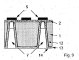
- the wafer consists of a SiC substrate 1 of about 250 to 400 microns thick thickness, on which an AlGaN / GaN layer stack 2 of about 2 to 3 microns thick is epitaxially grown.
- the terminal contacts of a transistor namely a drain contact 3, a gate contact 4 and a source contact 5.
- the potential of the source contact 5 must on the back (ground electrode 6) of the wafer, which takes place with the aid of a micro-vias 7 whose perforated walls 8 are metallized, so that the source contact 5 on the front side is electrically connected to the ground electrode 6 on the backside of the wafer.
- the process control of the process according to the invention and the results obtained are described below.
- the process sequence is in the Fig. 2 to 8 shown schematically.
- the finished processed GaN transistors or MMICs are provided in the wafer composite with the micro-vias 7.
- a protective varnish 9 is applied to the wafer front side in order to protect the wafers during the following process steps ( Fig. 2 ).
- the back surface is covered over a large area with a 2 ⁇ m thick protective layer 10 made of indium tin oxide (ITO) ( Fig. 3 ).
- ITO indium tin oxide
- This protective layer 10 then serves as protection of the SiC surface during etching and is removed during subsequent drilling by a laser at the via-inlet openings.
- Now blind holes 11 are drilled from the back side of the wafer with the laser ( FIG. 4 ).
- the laser beam which has a diameter of approximately 15 ⁇ m, is expediently moved on the wafer.
- the beam movement and laser parameters can be set in such a way that a surface profile that is as level as possible is formed close to the SiC / GaN interface.
- Loose particles that are deposited on the sample during the drilling process are then removed in a wet-chemical cleaning step. Etching in buffered hydrofluoric acid with ultrasound is suitable for this purpose.
- the blind holes 11 predrilled with the laser are then dry-chemically etched through plasma etching to the front-side contacts ( Fig. 5 ).
- the remaining SiC is removed by means of ICP etching in fluorine-containing gas mixtures (for example sulfur hexafluoride-oxygen-helium-SF 6 -O 2 -He).
- fluorine-containing gas mixtures for example sulfur hexafluoride-oxygen-helium-SF 6 -O 2 -He.
- the removal of the 2-3 ⁇ m thin epitaxial layer of AlGaN / GaN takes place plasma-chemically with an RIE process, for example with boron trichloride-chlorine (BCl 3 -Cl 2 ).
- the selectivity of the dry chemical etching process of GaN vs. Platinum is> 10: 1.
- the metal layer of the front side contact with a total thickness of about 5 microns is thus removed only very slowly, ie the etching process stops practically at Metal layer. An undercut does not occur.
- a lying below the platinum contacts titanium layer of some 10 nm is removed with.
- the possibly applied layer 10 can be removed again, which is expediently carried out with iron (III) chloride ( Fig. 6 ).
- a thin metal layer 12 is subsequently vapor-deposited on the wafer backside.
- a closed occupancy of the hole walls is achieved by Schrägbedampfung according to this embodiment.
- Other metallization processes such as sputtering or electroless chemical deposition are also possible.
- the plating base obtained by the metal layer 12 is then galvanically reinforced by a gold layer 5, typically 5 ⁇ m thick ( Fig. 7 ). In this way, an electrical connection is made from the one wafer side to the other side with a closed gold layer 13.
- an anti-wetting layer 14 made of titanium can also be applied to the via entry openings on the rear side, namely a titanium layer 100 nm thick, which is sputtered onto the existing gold layer 13.
- the anti-wetting layer 14 is applied to the wafer in a structured manner with the aid of a shadow mask.
- the shadow mask consists of a 0.1 mm thick metal foil in which holes are drilled with the laser.
- the layout of the openings in the metal foil corresponds to the arrangement of the micro-vias 7 on the wafer.
- the diameters of the openings in the shadow mask are slightly larger than the entry diameter of the micro-vias 7 on the back of the wafer, so that an approximately 40 ⁇ m wide titanium ring is formed around the via entry openings.
- the lacquering of the protective lacquer 9 can also take place only after the deposition of the anti-wetting layer 14 (titanium dewetting layer).
- FIG. 9 A schematic representation of the finished micro-vias 7 in cross-section shows Fig. 9 .
- the ITO masking of the surface can also be dispensed with if a controlled decrease in the material thickness during the etching process is acceptable, that is to say the steps according to FIGS 3 and 6 omitted.
- the process flow for this case is based on the 10 to 14 demonstrated.
- the process steps then correspond to process steps 1, 3, 4, 6 and 7 of the first example (corresponding to FIGS FIGS. 2, 4, 5, 7 and 8th ).
- the total thickness of the wafer decreases due to the large-area removal of the SiC.
- the wafer With an etching time of about 2 h, the wafer is thinned from 390 ⁇ m to 250-300 ⁇ m.
- an edge length of 35-70 microns is obtained, the corners are widened hexagonal.
- the hole shape is conical with a clear widening of the cross section at the entrance, whereby the subsequent occupancy of the hole wall is facilitated with metal.
- a frequency-tripled Nd: YAG laser is well suited for processing very hard and chemically inert SiC.
- This laser delivers nanosecond pulses of high energy in the ultraviolet spectral range at a wavelength of 355 nm with pulse rates of up to 100 kHz.
- the laser beam is moved micrometer-accurate by combining the CNC-controlled movement of the sample stage and the beam deflection with a galvo scanner.
- the laser beam can be positioned with an accuracy of ⁇ 1 ⁇ m with respect to existing structures on the workpiece. This precision is also achieved when the laser patterning is done on the back side and the alignment marks are on the (lower) front side.
- the edge length was about 75 microns at the laser entrance, at the hole bottom, it was about 15 microns, about 40 microns SiC remained below the bottom of the hole.
- Resistance measurements on a SiC sample prove that a low-resistance connection can be established between both sides.
- samples were first metallized on one side over the entire surface with a 5 ⁇ m thick gold layer before the via processing. From the other side, a matrix of vias was generated as described above. The hole spacing was 500 ⁇ m. Before measuring the resistance through a single hole, the individual holes had to be electrically separated from each other. For this purpose, the gold layer was cut through (scratched) to 500x500 microns 2 large fields, each with a via to get. It could be shown that the contacting through the SiC sample was realized with good reproducibility and very homogeneous.
- the resistance values are 25-31 m ⁇ .
- the mean value over the 206 micro-vias is 27 ⁇ 2 m ⁇ .
- the realized hollow rivets have an aspect ratio of 3-4.
- the prerequisite for the application of laser micromachining in the processing of semiconductor wafers is a high positioning accuracy of the beam center point of ⁇ 1 ⁇ m and better. This accuracy relates to the beam positioning relative to existing device structures and must be achieved in both the front and back side processing.
- the invention enables vias through the very hard and chemically resistant silicon carbide. An aspect ratio of 3-4 was demonstrated for this purpose.
Description
- Die Erfindung betrifft ein Verfahren zur Erzeugung von vertikalen Durchkontaktierungen (Mikro-Vias, Sacklochvias oder "blind" vias, via = vertical interconnect access) in Halbleiterwafern zur Herstellung von Halbleiter-Bauelementen, das heißt von Kontakten auf der Wafer-Vorderseite durch den Halbleiter-Wafer hindurch zur Wafer-Rückseite.
- Die vollständige Ausnutzung der Eigenschaften (zum Beispiel Hochfrequenzeigenschaften) der Bauelemente kann nur durch eine immer kompaktere Integration in die Peripherie erreicht werden. Kurze vertikale Verbindungen stellen einen effizienten Weg der elektrischen Kontaktierung dar. Außerdem ist es aus physikalischen Gründen erforderlich, zur Erhöhung der Verstärkung und der maximal pro Chip verfügbaren Ausgangsleistung von Hochleistungstransistoren eine elektrisch leitende Verbindung mit niedriger Induktivität zwischen den Source-Kontakten auf der Vorderseite und der Masseelektrode auf der Rückseite herzustellen. Dies lässt sich jedoch technologisch nicht immer leicht realisieren.
- Elektrisch aktives GaN-Material (Galliumnitrid) steht derzeit praktisch nicht als einkristallines Wafermaterial zur Verfügung und wird daher epitaktisch auf Substratmaterialien wie zum Beispiel SiC-Wafern (Siliciumcarbid) gewachsen.
- SiC zeichnet sich durch eine sehr gute Wärmeleitfähigkeit sowie eine extrem hohe chemische Stabilität und hohe Härte aus. Für eine Rückseitenkontaktierung von GaN-Transistoren besteht also die Notwendigkeit, das Trägermaterial aus SiC sowie die darüber liegende GaN-Epitaxieschicht zu durchbohren. Für eine Strukturierung kamen bisher praktisch nur trockenchemische Ätzverfahren wie reaktives Ionenätzen in eigens dafür optimierten Hochleistungs-Plasmaätzreaktoren in Frage. Typische Plasma-Ätzraten von SiC sind aber mit 1 µm/min sehr klein. Der Einsatz der Plasmaätztechnik setzt zudem die Herstellung und lithographische Strukturierung einer widerstandsfähigen Ätzmaske voraus.
- Es ist bekannt, dass sich in Leiterplatten Vias durch den Einsatz von Lasern herstellen lassen. Bei diesen Technologien werden mit dem Laser Öffnungen in die Kupfer- und Dielektrika-Schichten gebohrt und diese dann metallisiert, um elektrische Verbindungen zwischen bestimmten Lagen herzustellen. Die unterschiedlichen Lasertechnologien basieren auf dem Einsatz von CO2-Lasern, frequenzverdoppelten (grünen) YAG-Lasern, Excimerlasern und UV:YAG-Lasern.
- Die Herstellung dieser Vias ist beispielsweise beschrieben in:
- L. W. Burgess: "Introducing Via-in-Pad Blind Via Technology to Any PCB Multilayer Fabricator." IPC Printed Circuits Expo 1997, March 9-13, 1997, San Jose, CA, S15-2.
- A. Cable: "Improvements in High Speed Laser Microvia Formation Using Solid State Nd:YAG UV Lasers." IPC Printed Circuits Expo 1997, March 9-13, 1997, San Jose, CA, S17-7.
- M.D. Owen: "Via drilling." In: J.F. Ready, D.F. Farson (Edtrs.): LIA Handbook of laser materials processing, Laser Institute of America, Magnolia Publishing (2001) 661-665.
-
US 2001/035580 A1 beschäftigt sich mit der Durchkontaktierung von GaN-Halbleiterbauelementen auf Saphir- oder SiC-Substraten und kann zur Veranschaulichung des technischen Hintergrundes der Erfindung dienen. - Für die Erzeugung von Mikro-Vias in Halbleiterwafern ist aus der
US 2001/0035580 A1 eine Methode auf der Grundlage einer Lasertechnologie bekannt. - Der Erfindung liegt die Aufgabe zugrunde, ein effektives Verfahren zur Erzeugung von Mikro-Vias in Halbleiterwafern, insbesondere aus Materialien hoher Härte und chemischer Stabilität wie Siliciumcarbid, Saphir oder ähnlichem, anzugeben.
- Erfindungsgemäß wird die Aufgabe gelöst durch ein Verfahren mit den Merkmalen des Anspruchs 1. Zweckmäßige Ausgestaltungen sind Gegenstand der Unteransprüche.
- Danach ist das Verfahren gekennzeichnet durch die folgenden Schritte:
- Laserbohren von Sacklöchern an den Kontaktverbindungsstellen von der Wafer-Rückseite her in das Halbleitersubstrat
- Reinigung des Wafers (Entfernung des Debris)
- materialselektives Plasmaätzen des Halbleitersubstrates bis zum aktiven Schichtstapel des Wafers
- materialselektives Plasmaätzen des aktiven Schichtstapels des Wafers bis zum Erreichen der mit der Wafer-Rückseite zu verbindenden Kontakte
- Aufbringen einer Plattierbasis auf die Wafer-Rückseite und in die in einem vorhergehenden Schritt erzeugten Sacklöcher
- galvanischer Goldauftrag auf die metallisierte Wafer-Rückseite und die in einem vorhergehenden Schritt mit einer Plattierbasis versehenen Sacklöcher
- Um den Wafer während des Prozesses zu schützen, kann vorsorglich ein Schutzlack auf die Wafer-Vorderseite aufgebracht werden, der nach dem Prozess wieder entfernt wird (Ablacken).
- Um ein Abdünnen des Halbleitersubstrates beim Ätzen zu vermeiden, kann die Wafer-Rückseite vor dem Laserbohren der Sacklöcher mit Indium-Zinn-Oxid (ITO) beschichtet werden, das nach dem Plasmaätzen einfach wieder entfernt werden kann.
- Die Reinigung des Wafers zum Entfernen des Debris erfolgt im Falle von SiC-Substratmaterial zweckmäßig mit gepufferter Flusssäure.
- Als materialselektives Ätzverfahren für das Halbleitersubstrat eignet sich bevorzugt das ICP-Ätzverfahren (inductivelycoupled plasma), für den Schichtenstapel das RIE-Verfahren (reactiv ion etching).
- Als Laser eignet sich ein UV-Laser, bevorzugt ein frequenzverdreifachter Nd:YAG-Laser mit einer Wellenlänge von 355 nm.
- Das Aufbringen der Plattierbasis in die Mikro-Vias kann mit mehreren Methoden erfolgen. Bevorzugt wird eine Schrägbedampfung, eine chemische Badabscheidung (stromlos) oder ein Aufsputtern sind ebenfalls möglich.
- Im Bedarfsfall kann auf die Goldschicht lokal an den Mikro-Vias noch eine Antibenetzungsschicht (Dewettingschicht) aufgebracht werden. Für die Dewettingschicht wird zweckmäßig Titan verwendet, das aufgesputtert werden kann. Der Auftrag der Antibenetzungsschicht erfolgt zweckmäßig mit Hilfe einer Schattenmaske.
- Das Verfahren hat den Vorteil, dass Mikro-Vias in harten und chemisch inerten Substratmaterialien mit wesentlich verringertem Zeitaufwand und mit hoher Präzision erzeugt werden können.
- Mit dem erfindungsgemäßen Verfahren wird die Methode der Mikromaterialbearbeitung mittels UV-Laserstrahlung in Kombination mit Plasmaätzen ausgenutzt und für die direkte Strukturierung in der Bauelementefertigung eingesetzt. Im Gegensatz zur Erzeugung von Durchgangs-Vias (oder Hohlnieten-Vias) erfolgt hier keine vollständige Durchbohrung des Materials. Durch Plasmaätzen wird das Restmaterial bis zu den Kontakten der Vorderseite materialselektiv entfernt. Der besondere Vorteil liegt darin, dass eine widerstandsfähige
- Ätzmaske nicht lithografisch erzeugt werden muss, sondern die lasergebohrten Löcher als Ätzmaske dienen. Wenn die Bearbeitungsseite in geeigneter Weise geschützt wird, bleibt die Materialdicke erhalten. Eine Schutzschicht, die durch den Laser mit durchbohrt wird, verhindert in diesem Fall den flächigen Materialabtrag beim Plasmaätzen. Bei Verzicht auf die Schutzschicht, erfolgt ein großflächiger Ätzabtrag. Die damit einhergehende Abnahme der Materialdicke kann über die bekannten Ätzraten abgeschätzt werden.
- Die Erfindung soll anhand eines Ausführungsbeispiels näher erläutert werden. Die zugehörigen schematischen Zeichnungen zeigen die Phasen des erfindungsgemäßen Verfahrens am Beispiel einer Erzeugung von Mikro-Vias in Siliciumcarbid (SiC) für GaN-Hochleistungs-Feldeffekttransistoren oder MMICs, und zwar in
- Fig. 1
- den allgemeinen Aufbau eines Wafers mit einem Durchgangsloch (Via) im Querschnitt,
- Fig. 2 bis Fig. 8
- die einzelnen Schritte des Verfahrens,
- Fig. 9
- den Wafer mit den fertigen Mikro-Vias im Querschnitt und
- Fig. 10 bis Fig. 14
- die Schritte einer zweiten Variante des Verfahrens.
- In
Fig. 1 ist ein Wafer mit einem Transistoraufbau im Querschnitt gezeigt. Der Wafer besteht aus einem SiC-Substrat 1 von ca. 250 bis 400 µm Dicke, auf dem ein AlGaN/GaN-Schichtenstapel 2 von ca. 2 bis 3 µm Dicke epitaktisch aufgewachsen ist. Auf der Vorderseite des Wafers befinden sich auf dem Schichtenstapel 2 die Anschlusskontakte eines Transistors, nämlich ein Drain-Kontakt 3, ein Gate-Kontakt 4 und ein Source-Kontakt 5. Das Potential des Source-Kontakts 5 muss auf die Rückseite (Masseelektrode 6) des Wafers zurückgeführt werden, was mit Hilfe eines Mikro-Vias 7 erfolgt, dessen Lochwände 8 metallisiert sind, so dass der Source-Kontakt 5 auf der Vorderseite mit der Masseelektrode 6 auf der Rückseite des Wafers elektrisch verbunden wird. - Im Folgenden sollen die Prozessführung des erfindungsgemäßen Verfahrens und die erzielten Resultate beschrieben werden. Die Prozessfolge ist in den
Fig. 2 bis 8 schematisch dargestellt. Die fertig prozessierten GaN-Transistoren oder MMICs werden im Waferverbund mit den Mikro-Vias 7 versehen. Zunächst wird auf die Wafer-Vorderseite ein Schutzlack 9 aufgebracht, um die Wafer bei den folgenden Verfahrensschritten zu schützen (Fig. 2 ). Anschließend wird die Rückseite großflächig mit einer 2 µm dicken Schutzschicht 10 aus Indium-Zinn-Oxid (ITO) belegt (Fig. 3 ). Dieser Schritt ist jedoch nur notwendig, wenn sich die Dicke des Wafers bei der Strukturierung der Mikro-Vias 7 nicht ändern soll. Diese Schutzschicht 10 dient dann als Schutz der SiC-Oberfläche beim Ätzen und wird beim nachfolgenden Bohren durch einen Laser an den Via-Eintrittsöffnungen mit entfernt. Jetzt werden mit dem Laser Sacklöcher 11 von der Rückseite des Wafers her gebohrt (Fig. 4 ). Zur Herstellung der gewünschten Sacklöcher 11 wird der Laserstrahl, der einen Durchmesser von ca. 15 µm hat, zweckmäßig auf dem Wafer bewegt. Die Strahlbewegung und Laserparameter lassen sich so einstellen, dass ein möglichst ebenes Bodenprofil in der Nähe der SiC/GaN-Grenzfläche entsteht. - Lockere Partikel die sich beim Bohrprozess auf der Probe niederschlagen (Debris), werden anschließend in einem nasschemischen Reinigungsschritt entfernt. Hierzu eignet sich das Ätzen in gepufferter Flusssäure mit Ultraschall.
- Die mit dem Laser vorgebohrten Sacklöcher 11 werden anschließend durch Plasmaätzen bis an die Vorderseitenkontakte trockenchemisch durchgeätzt (
Fig. 5 ). Zweckmäßig wird das restliche SiC mittels ICP-Ätzen in fluorhaltigen Gasgemischen (zum Beispiel Schwefelhexafluorid-Sauerstoff-Helium - SF6-O2-He) entfernt. Durch Optimierung der Ätzparameter (Partialdrucke, Temperatur) lassen sich glatte Lochwände erhalten. Die Selektivität des Ätzprozesses von SiC vs. GaN ist >100:1, das heißt es lässt sich eine gute Homogenität der Ätzung über einen Wafer herstellen, da der Ätzprozess am GaN (Dicke ca. 2-3 µm) praktisch zum Halt kommt. - Die Entfernung der 2-3 µm dünnen Epitaxieschicht aus AlGaN/GaN (Schichtenstapel 2) erfolgt plasmachemisch mit einem RIE-Verfahren, zum Beispiel mit Bortrichlorid-Chlor (BCl3-Cl2). Die Selektivität des trockenchemischen Ätzprozesses von GaN vs. Platin ist >10:1. Die Metallschicht des Vorderseitenkontaktes mit einer Gesamtdicke von ca. 5 µm wird also nur sehr langsam abgetragen, d.h. der Ätzprozess stoppt praktisch an der Metallschicht. Eine Unterätzung tritt nicht auf. Eine unter den Platinkontakten liegende Titanschicht von einigen 10 nm wird mit abgetragen.
- Nach dem Ätzvorgang kann die eventuell aufgebrachte Schicht 10 (ITO) wieder entfernt werden, was zweckmäßig mit Eisen-III-Chlorid erfolgt (
Fig 6 ). - Auf die Wafer-Rückseite wird nachfolgend eine dünne Metallschicht 12 aufgedampft. Dabei wird nach diesem Ausführungsbeispiel durch Schrägbedampfung eine geschlossene Belegung der Lochwände erzielt. Andere Metallisierungsprozesse wie Sputtern oder eine stromlose chemische Abscheidung sind ebenfalls möglich. Die durch die Metallschicht 12 erhaltene Plattierbasis wird anschließend durch eine typisch 5 µm dicke Goldschicht 13 galvanisch verstärkt (
Fig. 7 ). Auf diese Weise wird eine elektrische Verbindung von der einen Waferseite zur anderen Seite mit einer geschlossenen Goldschicht 13 hergestellt. - Nach dem Metallisieren erfolgt in einem weiteren Prozessschritt das Ablacken des Schutzlackes 9 (
Fig. 8 ). - Bei Bedarf kann an den Via-Eintrittsöffnungen auf der Rückseite noch eine Antibenetzungsschicht 14 aus Titan aufgebracht werden, nämlich eine 100 nm dünne Titanschicht, die auf die vorhandene Goldschicht 13 gesputtert wird. Die Antibenetzungsschicht 14 wird mit Hilfe einer Schattenmaske strukturiert auf den Wafer aufgebracht. Die Schattenmaske besteht aus einer 0.1 mm dicken Metallfolie, in die mit dem Laser Öffnungen gebohrt werden. Das Layout der Öffnungen in der Metallfolie entspricht der Anordnung der Mikro-Vias 7 auf dem Wafer. Die Durchmesser der Öffnungen in der Schattenmaske sind etwas größer als der Eintrittsdurchmesser der Mikro-Vias 7 auf der Wafer-Rückseite, so dass sich ein etwa 40 µm breiter Titan-Ring um die Via-Eintrittsöffnungen ausbildet. Mit Hilfe von je vier zusätzlichen Durchgangsbohrungen am Rand von Schattenmaske und Wafer werden beide Teile mittels Passstiften zueinander justiert, das heißt deckungsgleich gebracht.
- Es ist anzumerken, dass das Ablacken des Schutzlacks 9 auch erst nach der Abscheidung der Antibenetzungsschicht 14 (Titan-Dewettingschicht) erfolgen kann.
- Eine schematische Darstellung der fertigen Mikro-Vias 7 im Querschnitt zeigt
Fig. 9 . - Auf die ITO-Maskierung der Oberfläche (Schutzschicht 10) kann auch verzichtet werden, falls eine kontrollierte Abnahme der Materialdicke beim Ätzprozess akzeptabel ist, das heißt die Schritte gemäß den
Fig. 3 und 6 entfallen. - Der Prozessablauf für diesen Fall wird anhand der
Fig. 10 bis 14 demonstriert. Die Prozessschritte entsprechen dann den Prozessschritten 1, 3, 4, 6 und 7 des ersten Beispiels (entsprechend denFiguren 2, 4, 5, 7 und8 ). - In diesem Fall nimmt die Gesamtdicke des Wafers durch die großflächige Entfernung des SiC ab. Bei einer Ätzdauer von ca. 2 h wird der Wafer von 390 µm auf 250-300 µm abgedünnt. Am Lochboden wird eine Kantenlänge von 35-70 µm erhalten, wobei die Ecken hexagonal aufgeweitet sind. Die Lochform ist konisch mit einer deutlichen Aufweitung des Querschnittes am Eintritt, wodurch die nachträgliche Belegung der Lochwand mit Metall erleichtert wird.
- Im Hinblick auf Abtragsrate, Flexibilität und Zuverlässigkeit ist ein frequenzverdreifachter Nd:YAG-Laser für die Bearbeitung des sehr harten und chemisch inerten SiC gut geeignet. Dieser Laser liefert Nanosekundenpulse mit hoher Energie im ultravioletten Spektralbereich bei einer Wellenlänge von 355 nm mit Pulsfrequenzen von bis zu 100 kHz. Der Laserstrahl wird durch Kombination der CNC-gesteuerten Bewegung des Probentisches und der Strahlablenkung mit einem Galvo-Scanner mikrometergenau bewegt. Mit Hilfe einer Bilderkennung und eines hochgenauen luftgelagerten XY-Kreuztisches kann der Laserstrahl mit einer Genauigkeit von ±1 µm in bezug auf vorhandene Strukturen auf dem Werkstück positioniert werden. Diese Präzision wird auch erreicht, wenn die Laserstrukturierung auf der Rückseite erfolgt und sich die Justagemarken auf der (untenliegenden) Vorderseite befinden.
- Mit dem Laser wurden Sacklöcher gebohrt, die einen quadratischen Querschnitt und einen möglichst ebenen Lochboden haben. Die Kantenlänge betrug ca. 75 µm an der Lasereintrittsöffnung, am Lochboden betrug sie ca. 15 µm, ca. 40 µm SiC blieben unterhalb des Lochbodens stehen.
- Es wurde ein automatisiertes Bohrverfahren verwendet, bei dem die jeweilige Bearbeitungsstelle der Probe durch präzises Verfahren des Probentisches mikrometergenau unter dem Strahlaustritt positioniert wird und der Laserstrahl dann durch ein Spiegelsystem (Galvo-Scanner) schnell auf dem Werkstück bewegt wird, wobei 250-450 µm dickes SiC verwendet wurde. Im Rasterelektronenmikroskop lässt sich gut erkennen, dass die lasergebohrten Löcher leicht konisch sind und sich eine glatte Wand mit wenig Ablagerungen erzeugen lässt.
- Widerstandsmessungen an einer SiC-Probe belegen, dass sich eine niederohmige Verbindung zwischen beiden Seiten herstellen lässt. Dazu wurden Proben vor der Via-Prozessierung zunächst auf einer Seite ganzflächig mit einer 5 µm dicken Goldschicht metallisiert. Von der anderen Seite wurde wie oben beschrieben eine Matrix von Vias erzeugt. Der Lochabstand betrug 500 µm. Vor der Messung des Widerstandes durch ein einzelnes Loch mussten die einzelnen Löcher dann noch elektrisch voneinander separiert werden. Dazu wurde die Goldschicht durchtrennt (geritzt), um 500x500 µm2 große Felder mit je einem Via zu erhalten. Es konnte gezeigt werden, dass die Kontaktierung durch die SiC-Probe hindurch mit guter Reproduzierbarkeit und sehr homogen realisiert wurde. Die Widerstandswerte liegen bei 25-31 mΩ. Der Mittelwert über die 206 Mikro-Vias liegt bei 27±2 mΩ. Die realisierten Hohlnieten haben ein Aspektverhältnis von 3-4.
- In Tests an aufgebauten Transistoren verschiedenen Typs wurde die Funktionstüchtigkeit der Bauelemente nachgewiesen. Anhand der Transistor-Kennlinien wurde der Nachweis für die erfolgreiche Implementierung des Laserbohrens von Mikro-Vias in die GaN-Prozesstechnologie geführt.
- Die technologischen Untersuchungen zeigen die Machbarkeit von lasergebohrten Mikro-Vias durch einkristallines SiC-Wafermaterial für GaN-Hochleistungs-Feldeffekttransistoren. Es konnte nachgewiesen werden, dass sich die Lasermikrostrukturierung in die Bauelemente-Prozesstechnologie erfolgreich implementieren lässt.
- Voraussetzung für die Anwendung der Laser-Mikrobearbeitung in der Prozessierung von Halbleiter-Wafern ist eine hohe Positioniergenauigkeit des Strahlmittelpunktes von ± 1µm und besser. Diese Genauigkeit bezieht sich auf die Strahlpositionierung relativ zu vorhandenen Bauelementestrukturen und muss sowohl bei der Bearbeitung von der Vorderseite wie auch von der Rückseite erzielt werden.
- Die Erfindung ermöglicht Durchkontaktierungen durch das sehr harte und chemisch beständige Siliciumcarbid. Ein Aspektverhältnis von 3-4 wurde hierfür demonstriert.
-
- 1
- SiC-Substrat
- 2
- AlGaN/GaN-Schichtenstapel
- 3
- Drain-Kontakt
- 4
- Gate-Kontakt
- 5
- Source-Kontakt
- 6
- Masseelektrode
- 7
- Mikro-Via
- 8
- Lochwand
- 9
- Schutzlack
- 10
- Schutzschicht (ITO)
- 11
- Sacklöcher
- 12
- Metallschicht
- 13
- Goldschicht
- 14
- Antibenetzungsschicht
Claims (15)
- Verfahren zur Erzeugung von vertikalen Durchkontaktierungen zur Herstellung von Halbleiter-Bauelementen, das heißt von Kontakten auf der Wafer-Vorderseite durch den Halbleiter-Wafer hindurch zur Wafer-Rückseite, wobei der Wafer ein Substrat (1) aus einem Substratmaterial und einen auf das Substrat (1) aufgebrachten elektrisch aktiven Schichtenstapel (2) mit einer GaN-Epitaxieschicht aufweist,
die folgenden Schritte umfassend:- Laserbohren von Sacklöchern (11) an den Kontaktverbindungsstellen von der Wafer-Rückseite (6) her in das Halbleitersubstrat- Reinigung des Wafers- materialselektives Plasmaätzen des Halbleitersubstrates bis zum aktiven Schichtstapel des Wafers- materialselektives Plasmaätzen des aktiven Schichtstapels (2) des Wafers bis zum Erreichen der mit der Wafer-Rückseite (6) zu verbindenden Kontakte- Aufbringen einer Plattierbasis (12) auf die Wafer-Rückseite (6) und in die in einem vorhergehenden Schritt erzeugten Sacklöcher (11)- galvanischer Goldauftrag (13) auf die metallisierte Wafer-Rückseite (6) und die in einem vorhergehenden Schritt mit einer Plattierbasis (12)versehenen Sacklöcher (11). - Verfahren nach Anspruch 1, dadurch gekennzeichnet, dass
vor dem Laserbohren der Sacklöcher (11) auf die Wafer-Vorderseite ein Schutzlack (9) aufgebracht wird, der nach dem Goldauftrag (13) wieder entfernt wird. - Verfahren nach Anspruch 1 oder 2, dadurch gekennzeichnet, dass
die Wafer-Rückseite (6) vor dem Laserbohren der Sacklöcher (11) mit Indium-Zinn-Oxid (ITO) beschichtet wird, das nach dem Goldauftrag (13) wieder entfernt wird. - Verfahren nach einem der Ansprüche 1 bis 3, dadurch gekennzeichnet, dass
die Reinigung nasschemisch mittels gepufferter Flusssäure erfolgt. - Verfahren nach einem der vorhergehenden Ansprüche, dadurch gekennzeichnet, dass
im Bereich der Eintrittsöffnungen der Durchgangslöcher an der Wafer-Rückseite (6) eine Antibenetzungsschicht (14) auf den galvanischen Goldauftrag (13) aufgebracht wird. - Verfahren nach Anspruch 5, dadurch gekennzeichnet, dass für die Antibenetzungsschicht (14) Titan verwendet wird.
- Verfahren nach Anspruch 5 oder 6, dadurch gekennzeichnet, dass die Antibenetzungsschicht (14) aufgesputtert wird.
- Verfahren nach einem der Ansprüche 5 bis 7, dadurch gekennzeichnet, dass
der Auftrag der Antibenetzungsschicht (14) mit Hilfe einer Schattenmaske erfolgt. - Verfahren nach einem der vorhergehenden Ansprüche, dadurch gekennzeichnet, dass
zum Laserbohren ein UV-Laser verwendet wird. - Verfahren nach einem der vorhergehenden Ansprüche, dadurch gekennzeichnet, dass
der Auftrag der Plattierbasis (12) durch Schrägaufdampfen erfolgt. - Verfahren nach einem der Ansprüche 1 bis 9, dadurch gekennzeichnet, dass
der Auftrag der Plattierbasis (12) durch Sputtern erfolgt. - Verfahren nach einem der Ansprüche 1 bis 9, dadurch gekennzeichnet, dass
der Auftrag der Plattierbasis (12) durch chemische Badabscheidung erfolgt. - Verfahren nach einem der vorhergehenden Ansprüche, dadurch gekennzeichnet, dass
zum Laserbohren ein Laser benutzt wird, dessen Strahl kleiner ist als die Querschnittsfläche des zu erzeugenden Sackloches (11), wobei der Strahl über den Bereich des Sackloches (11) bewegt wird. - Verfahren nach einem der vorhergehenden Ansprüche, dadurch gekennzeichnet, dass
das Plasmaätzen des Halbleitersubstrates durch ICP-Ätzen erfolgt. - Verfahren nach einem der vorhergehenden Ansprüche, dadurch gekennzeichnet, dass
das Plasmaätzen des aktiven Schichtenstapels (2) durch RIE-Ätzen erfolgt.
Applications Claiming Priority (2)
| Application Number | Priority Date | Filing Date | Title |
|---|---|---|---|
| DE102005042074A DE102005042074A1 (de) | 2005-08-31 | 2005-08-31 | Verfahren zur Erzeugung von Durchkontaktierungen in Halbleiterwafern |
| PCT/EP2006/064599 WO2007025812A1 (de) | 2005-08-31 | 2006-07-24 | Verfahren zur erzeugung von durchkontaktierungen in halbleiterwafern |
Publications (2)
| Publication Number | Publication Date |
|---|---|
| EP1920461A1 EP1920461A1 (de) | 2008-05-14 |
| EP1920461B1 true EP1920461B1 (de) | 2016-11-16 |
Family
ID=37076379
Family Applications (1)
| Application Number | Title | Priority Date | Filing Date |
|---|---|---|---|
| EP06792559.4A Not-in-force EP1920461B1 (de) | 2005-08-31 | 2006-07-24 | Verfahren zur erzeugung von durchkontaktierungen in halbleiterwafern |
Country Status (5)
| Country | Link |
|---|---|
| US (1) | US8455355B2 (de) |
| EP (1) | EP1920461B1 (de) |
| JP (1) | JP5123185B2 (de) |
| DE (1) | DE102005042074A1 (de) |
| WO (1) | WO2007025812A1 (de) |
Families Citing this family (31)
| Publication number | Priority date | Publication date | Assignee | Title |
|---|---|---|---|---|
| US7091124B2 (en) | 2003-11-13 | 2006-08-15 | Micron Technology, Inc. | Methods for forming vias in microelectronic devices, and methods for packaging microelectronic devices |
| US8084866B2 (en) | 2003-12-10 | 2011-12-27 | Micron Technology, Inc. | Microelectronic devices and methods for filling vias in microelectronic devices |
| US20050247894A1 (en) | 2004-05-05 | 2005-11-10 | Watkins Charles M | Systems and methods for forming apertures in microfeature workpieces |
| US7232754B2 (en) | 2004-06-29 | 2007-06-19 | Micron Technology, Inc. | Microelectronic devices and methods for forming interconnects in microelectronic devices |
| SG120200A1 (en) | 2004-08-27 | 2006-03-28 | Micron Technology Inc | Slanted vias for electrical circuits on circuit boards and other substrates |
| US7300857B2 (en) | 2004-09-02 | 2007-11-27 | Micron Technology, Inc. | Through-wafer interconnects for photoimager and memory wafers |
| US7271482B2 (en) | 2004-12-30 | 2007-09-18 | Micron Technology, Inc. | Methods for forming interconnects in microelectronic workpieces and microelectronic workpieces formed using such methods |
| US7795134B2 (en) | 2005-06-28 | 2010-09-14 | Micron Technology, Inc. | Conductive interconnect structures and formation methods using supercritical fluids |
| US7262134B2 (en) | 2005-09-01 | 2007-08-28 | Micron Technology, Inc. | Microfeature workpieces and methods for forming interconnects in microfeature workpieces |
| US7863187B2 (en) | 2005-09-01 | 2011-01-04 | Micron Technology, Inc. | Microfeature workpieces and methods for forming interconnects in microfeature workpieces |
| US7749899B2 (en) | 2006-06-01 | 2010-07-06 | Micron Technology, Inc. | Microelectronic workpieces and methods and systems for forming interconnects in microelectronic workpieces |
| US7629249B2 (en) | 2006-08-28 | 2009-12-08 | Micron Technology, Inc. | Microfeature workpieces having conductive interconnect structures formed by chemically reactive processes, and associated systems and methods |
| US7902643B2 (en) | 2006-08-31 | 2011-03-08 | Micron Technology, Inc. | Microfeature workpieces having interconnects and conductive backplanes, and associated systems and methods |
| DE102007019552B4 (de) * | 2007-04-25 | 2009-12-17 | Infineon Technologies Ag | Verfahren zur Herstellung eines Substrats mit Durchführung sowie Substrat und Halbleitermodul mit Durchführung |
| JP5228381B2 (ja) * | 2007-06-25 | 2013-07-03 | 三菱電機株式会社 | 半導体装置の製造方法 |
| SG149710A1 (en) | 2007-07-12 | 2009-02-27 | Micron Technology Inc | Interconnects for packaged semiconductor devices and methods for manufacturing such devices |
| SG150410A1 (en) | 2007-08-31 | 2009-03-30 | Micron Technology Inc | Partitioned through-layer via and associated systems and methods |
| US7884015B2 (en) | 2007-12-06 | 2011-02-08 | Micron Technology, Inc. | Methods for forming interconnects in microelectronic workpieces and microelectronic workpieces formed using such methods |
| US20100321238A1 (en) * | 2009-06-18 | 2010-12-23 | Lin-Ping Shen | Butler matrix and beam forming antenna comprising same |
| US20110209432A1 (en) * | 2010-03-01 | 2011-09-01 | Downey Mike A | Metal "slip clip" to hold metal studes in top track of commercial interior framing |
| CN101916754B (zh) * | 2010-06-29 | 2012-08-29 | 香港应用科技研究院有限公司 | 通孔和通孔形成方法以及通孔填充方法 |
| JP5566803B2 (ja) * | 2010-07-21 | 2014-08-06 | 住友電工デバイス・イノベーション株式会社 | 半導体装置の製造方法 |
| KR101219386B1 (ko) * | 2011-02-16 | 2013-01-21 | 한국기계연구원 | 관통형 실리콘 비아의 가공방법 및 그에 의해 제조된 반도체 칩 |
| JP2013058624A (ja) * | 2011-09-08 | 2013-03-28 | Mitsubishi Electric Corp | レーザダイオード素子の製造方法 |
| CN102768950A (zh) * | 2012-07-12 | 2012-11-07 | 江苏扬景光电有限公司 | 一种混合式蚀刻产生氮化物器件衬底的孔洞的方法 |
| KR101988893B1 (ko) * | 2012-12-12 | 2019-09-30 | 한국전자통신연구원 | 반도체 소자 및 이를 제조하는 방법 |
| JP6309211B2 (ja) * | 2013-06-14 | 2018-04-11 | 新電元工業株式会社 | 炭化ケイ素半導体装置 |
| JP2015002299A (ja) * | 2013-06-17 | 2015-01-05 | 株式会社ザイキューブ | 漏斗状の貫通電極およびその製造方法 |
| CN107980171B (zh) * | 2016-12-23 | 2022-06-24 | 苏州能讯高能半导体有限公司 | 半导体芯片、半导体晶圆及半导体晶圆的制造方法 |
| US10269756B2 (en) * | 2017-04-21 | 2019-04-23 | Invensas Bonding Technologies, Inc. | Die processing |
| WO2020136808A1 (ja) * | 2018-12-27 | 2020-07-02 | 三菱電機株式会社 | 半導体素子構造 |
Family Cites Families (20)
| Publication number | Priority date | Publication date | Assignee | Title |
|---|---|---|---|---|
| US4473737A (en) * | 1981-09-28 | 1984-09-25 | General Electric Company | Reverse laser drilling |
| US4897708A (en) * | 1986-07-17 | 1990-01-30 | Laser Dynamics, Inc. | Semiconductor wafer array |
| US5371042A (en) * | 1992-06-16 | 1994-12-06 | Applied Materials, Inc. | Method of filling contacts in semiconductor devices |
| JP3724110B2 (ja) * | 1997-04-24 | 2005-12-07 | 三菱電機株式会社 | 半導体装置の製造方法 |
| JP4264992B2 (ja) * | 1997-05-28 | 2009-05-20 | ソニー株式会社 | 半導体装置の製造方法 |
| US6239033B1 (en) * | 1998-05-28 | 2001-05-29 | Sony Corporation | Manufacturing method of semiconductor device |
| JP2868008B1 (ja) * | 1997-11-21 | 1999-03-10 | 日本電気株式会社 | 半導体装置及びその製造方法 |
| EP0926723B1 (de) * | 1997-11-26 | 2007-01-17 | STMicroelectronics S.r.l. | Herstellungsverfahren für einen Vorder-Hinterseiten-Durchkontakt in mikro-integrierten Schaltungen |
| JPH11238870A (ja) * | 1998-02-20 | 1999-08-31 | Nec Corp | 半導体装置とその製造方法 |
| US6475889B1 (en) * | 2000-04-11 | 2002-11-05 | Cree, Inc. | Method of forming vias in silicon carbide and resulting devices and circuits |
| US7125786B2 (en) * | 2000-04-11 | 2006-10-24 | Cree, Inc. | Method of forming vias in silicon carbide and resulting devices and circuits |
| US20020086520A1 (en) * | 2001-01-02 | 2002-07-04 | Advanced Semiconductor Engineering Inc. | Semiconductor device having bump electrode |
| WO2002060636A1 (en) * | 2001-01-31 | 2002-08-08 | Electro Scientific Industries, Inc. | Ultraviolet laser ablative patterning of microstructures in semiconductors |
| US7233028B2 (en) * | 2001-02-23 | 2007-06-19 | Nitronex Corporation | Gallium nitride material devices and methods of forming the same |
| JP4053257B2 (ja) * | 2001-06-14 | 2008-02-27 | 新光電気工業株式会社 | 半導体装置の製造方法 |
| US6902872B2 (en) * | 2002-07-29 | 2005-06-07 | Hewlett-Packard Development Company, L.P. | Method of forming a through-substrate interconnect |
| US6903442B2 (en) * | 2002-08-29 | 2005-06-07 | Micron Technology, Inc. | Semiconductor component having backside pin contacts |
| US6936536B2 (en) * | 2002-10-09 | 2005-08-30 | Micron Technology, Inc. | Methods of forming conductive through-wafer vias |
| US6841883B1 (en) * | 2003-03-31 | 2005-01-11 | Micron Technology, Inc. | Multi-dice chip scale semiconductor components and wafer level methods of fabrication |
| US7674719B2 (en) * | 2005-08-01 | 2010-03-09 | Panasonic Corporation | Via hole machining for microwave monolithic integrated circuits |
-
2005
- 2005-08-31 DE DE102005042074A patent/DE102005042074A1/de not_active Withdrawn
-
2006
- 2006-07-24 JP JP2008528445A patent/JP5123185B2/ja not_active Expired - Fee Related
- 2006-07-24 EP EP06792559.4A patent/EP1920461B1/de not_active Not-in-force
- 2006-07-24 US US11/993,459 patent/US8455355B2/en active Active
- 2006-07-24 WO PCT/EP2006/064599 patent/WO2007025812A1/de active Application Filing
Non-Patent Citations (1)
| Title |
|---|
| None * |
Also Published As
| Publication number | Publication date |
|---|---|
| JP5123185B2 (ja) | 2013-01-16 |
| US8455355B2 (en) | 2013-06-04 |
| EP1920461A1 (de) | 2008-05-14 |
| JP2009506561A (ja) | 2009-02-12 |
| DE102005042074A1 (de) | 2007-03-08 |
| US20080286963A1 (en) | 2008-11-20 |
| WO2007025812A1 (de) | 2007-03-08 |
Similar Documents
| Publication | Publication Date | Title |
|---|---|---|
| EP1920461B1 (de) | Verfahren zur erzeugung von durchkontaktierungen in halbleiterwafern | |
| EP1891670B1 (de) | Verfahren zur Erzeugung von vertikalen elektrischen Kontaktverbindungen in Halbleiterwafern | |
| DE10101875B4 (de) | Elektronisches Bauteil mit aufeinander gestapelten Halbleiterchips und Verfahren zu seiner Herstellung | |
| DE102014107557B4 (de) | Verfahren zum Bearbeiten eines Halbleiterwerkstücks | |
| WO2005101928A1 (de) | Hybrider leiterplattenaufbau zur kompakten aufbautechnik von elektrischen bauelementen | |
| DE102015100491B4 (de) | Vereinzelung von Halbleiter-Dies mit Kontaktmetallisierung durch elektroerosive Bearbeitung | |
| DE102009004451A1 (de) | Elektronikbauelement und Verfahren zu dessen Herstellung | |
| DE102012214254A1 (de) | Laserbasiertes Verfahren und Bearbeitungstisch zur lokalen Kontaktierung eines Halbleiterbauelements | |
| DE60033353T2 (de) | Elektronisches gerät und herstellung | |
| DE102017107648A1 (de) | Elektrische Durchkontaktierung(en) in einem Halbleitersubstrat und ein zugehöriges Herstellverfahren | |
| EP2095698B1 (de) | Verfahren zur herstellung von durchkontaktierungen und leiterbahnen | |
| DE102020206233B3 (de) | Verfahren zum herstellen eines substrats und system zum herstellen eines substrats | |
| DE102015218842A1 (de) | Verfahren zur Kontaktierung einer Kontaktfläche eines Halbleiterbauteils und Elektronikmodul | |
| DE10244077B4 (de) | Verfahren zur Herstellung von Halbleiterbauteilen mit Durchkontaktierung | |
| EP1111671B1 (de) | Verfahren zum Herstellen einer Halbleiteranordnung | |
| DE102011005642A1 (de) | Verfahren zum Schutz von reaktiven Metalloberflächen von Halbleiterbauelementen während des Transports durch Bereitstellen einer zusätzlichen Schutzschicht | |
| WO1995026852A1 (de) | Verfahren und vorrichtung zur herstellung einer lötbaren metallisierungsschicht auf einer nichtlötbaren oberfläche | |
| WO2005101480A2 (de) | Mit planarer verbindungstechnik auf einem insbesondere elektrisch leitendem substrat aufgebaute schaltung | |
| EP2028686B1 (de) | Verfahren zum galvanischen Aufbringen eines Metalls, insbesondere von Kupfer, und Verwendung dieses Verfahrens | |
| WO2005101490A2 (de) | An einer kühlrippe angeordnetes bauelement | |
| DE19715501C1 (de) | Verfahren zur Strukturierung von dünnen Metallschichten | |
| WO1999005721A1 (de) | Halbleiterchippackungen und verfahren zu deren herstellung | |
| DE10160604A1 (de) | Verfahren zur Herstellung einer Kühlvertiefung in einem Halbleiterprodukt | |
| DE102022113636A1 (de) | Elektrisches Modul | |
| DE3243307A1 (de) | Halbleiter-bauelemente und verfahren zu ihrer herstellung |
Legal Events
| Date | Code | Title | Description |
|---|---|---|---|
| PUAI | Public reference made under article 153(3) epc to a published international application that has entered the european phase |
Free format text: ORIGINAL CODE: 0009012 |
|
| 17P | Request for examination filed |
Effective date: 20080219 |
|
| AK | Designated contracting states |
Kind code of ref document: A1 Designated state(s): AT BE BG CH CY CZ DE DK EE ES FI FR GB GR HU IE IS IT LI LT LU LV MC NL PL PT RO SE SI SK TR |
|
| 17Q | First examination report despatched |
Effective date: 20091221 |
|
| DAX | Request for extension of the european patent (deleted) | ||
| GRAP | Despatch of communication of intention to grant a patent |
Free format text: ORIGINAL CODE: EPIDOSNIGR1 |
|
| RIC1 | Information provided on ipc code assigned before grant |
Ipc: H01L 21/768 20060101AFI20160608BHEP Ipc: H01L 21/302 20060101ALI20160608BHEP |
|
| INTG | Intention to grant announced |
Effective date: 20160623 |
|
| GRAS | Grant fee paid |
Free format text: ORIGINAL CODE: EPIDOSNIGR3 |
|
| GRAJ | Information related to disapproval of communication of intention to grant by the applicant or resumption of examination proceedings by the epo deleted |
Free format text: ORIGINAL CODE: EPIDOSDIGR1 |
|
| GRAL | Information related to payment of fee for publishing/printing deleted |
Free format text: ORIGINAL CODE: EPIDOSDIGR3 |
|
| GRAR | Information related to intention to grant a patent recorded |
Free format text: ORIGINAL CODE: EPIDOSNIGR71 |
|
| GRAA | (expected) grant |
Free format text: ORIGINAL CODE: 0009210 |
|
| INTG | Intention to grant announced |
Effective date: 20161006 |
|
| AK | Designated contracting states |
Kind code of ref document: B1 Designated state(s): AT BE BG CH CY CZ DE DK EE ES FI FR GB GR HU IE IS IT LI LT LU LV MC NL PL PT RO SE SI SK TR |
|
| REG | Reference to a national code |
Ref country code: GB Ref legal event code: FG4D Free format text: NOT ENGLISH |
|
| REG | Reference to a national code |
Ref country code: CH Ref legal event code: EP |
|
| REG | Reference to a national code |
Ref country code: IE Ref legal event code: FG4D Free format text: LANGUAGE OF EP DOCUMENT: GERMAN |
|
| REG | Reference to a national code |
Ref country code: AT Ref legal event code: REF Ref document number: 846632 Country of ref document: AT Kind code of ref document: T Effective date: 20161215 |
|
| REG | Reference to a national code |
Ref country code: DE Ref legal event code: R096 Ref document number: 502006015245 Country of ref document: DE |
|
| REG | Reference to a national code |
Ref country code: DE Ref legal event code: R096 Ref document number: 502006015245 Country of ref document: DE |
|
| REG | Reference to a national code |
Ref country code: NL Ref legal event code: FP |
|
| PG25 | Lapsed in a contracting state [announced via postgrant information from national office to epo] |
Ref country code: LV Free format text: LAPSE BECAUSE OF FAILURE TO SUBMIT A TRANSLATION OF THE DESCRIPTION OR TO PAY THE FEE WITHIN THE PRESCRIBED TIME-LIMIT Effective date: 20161116 |
|
| REG | Reference to a national code |
Ref country code: SE Ref legal event code: TRGR |
|
| REG | Reference to a national code |
Ref country code: LT Ref legal event code: MG4D |
|
| PG25 | Lapsed in a contracting state [announced via postgrant information from national office to epo] |
Ref country code: GR Free format text: LAPSE BECAUSE OF FAILURE TO SUBMIT A TRANSLATION OF THE DESCRIPTION OR TO PAY THE FEE WITHIN THE PRESCRIBED TIME-LIMIT Effective date: 20170217 Ref country code: LT Free format text: LAPSE BECAUSE OF FAILURE TO SUBMIT A TRANSLATION OF THE DESCRIPTION OR TO PAY THE FEE WITHIN THE PRESCRIBED TIME-LIMIT Effective date: 20161116 |
|
| PG25 | Lapsed in a contracting state [announced via postgrant information from national office to epo] |
Ref country code: PT Free format text: LAPSE BECAUSE OF FAILURE TO SUBMIT A TRANSLATION OF THE DESCRIPTION OR TO PAY THE FEE WITHIN THE PRESCRIBED TIME-LIMIT Effective date: 20170316 Ref country code: ES Free format text: LAPSE BECAUSE OF FAILURE TO SUBMIT A TRANSLATION OF THE DESCRIPTION OR TO PAY THE FEE WITHIN THE PRESCRIBED TIME-LIMIT Effective date: 20161116 Ref country code: PL Free format text: LAPSE BECAUSE OF FAILURE TO SUBMIT A TRANSLATION OF THE DESCRIPTION OR TO PAY THE FEE WITHIN THE PRESCRIBED TIME-LIMIT Effective date: 20161116 Ref country code: FI Free format text: LAPSE BECAUSE OF FAILURE TO SUBMIT A TRANSLATION OF THE DESCRIPTION OR TO PAY THE FEE WITHIN THE PRESCRIBED TIME-LIMIT Effective date: 20161116 |
|
| REG | Reference to a national code |
Ref country code: FR Ref legal event code: PLFP Year of fee payment: 12 |
|
| PG25 | Lapsed in a contracting state [announced via postgrant information from national office to epo] |
Ref country code: SK Free format text: LAPSE BECAUSE OF FAILURE TO SUBMIT A TRANSLATION OF THE DESCRIPTION OR TO PAY THE FEE WITHIN THE PRESCRIBED TIME-LIMIT Effective date: 20161116 Ref country code: DK Free format text: LAPSE BECAUSE OF FAILURE TO SUBMIT A TRANSLATION OF THE DESCRIPTION OR TO PAY THE FEE WITHIN THE PRESCRIBED TIME-LIMIT Effective date: 20161116 Ref country code: RO Free format text: LAPSE BECAUSE OF FAILURE TO SUBMIT A TRANSLATION OF THE DESCRIPTION OR TO PAY THE FEE WITHIN THE PRESCRIBED TIME-LIMIT Effective date: 20161116 Ref country code: EE Free format text: LAPSE BECAUSE OF FAILURE TO SUBMIT A TRANSLATION OF THE DESCRIPTION OR TO PAY THE FEE WITHIN THE PRESCRIBED TIME-LIMIT Effective date: 20161116 Ref country code: CZ Free format text: LAPSE BECAUSE OF FAILURE TO SUBMIT A TRANSLATION OF THE DESCRIPTION OR TO PAY THE FEE WITHIN THE PRESCRIBED TIME-LIMIT Effective date: 20161116 |
|
| REG | Reference to a national code |
Ref country code: DE Ref legal event code: R097 Ref document number: 502006015245 Country of ref document: DE |
|
| PG25 | Lapsed in a contracting state [announced via postgrant information from national office to epo] |
Ref country code: BG Free format text: LAPSE BECAUSE OF FAILURE TO SUBMIT A TRANSLATION OF THE DESCRIPTION OR TO PAY THE FEE WITHIN THE PRESCRIBED TIME-LIMIT Effective date: 20170216 |
|
| PLBE | No opposition filed within time limit |
Free format text: ORIGINAL CODE: 0009261 |
|
| STAA | Information on the status of an ep patent application or granted ep patent |
Free format text: STATUS: NO OPPOSITION FILED WITHIN TIME LIMIT |
|
| 26N | No opposition filed |
Effective date: 20170817 |
|
| PG25 | Lapsed in a contracting state [announced via postgrant information from national office to epo] |
Ref country code: SI Free format text: LAPSE BECAUSE OF FAILURE TO SUBMIT A TRANSLATION OF THE DESCRIPTION OR TO PAY THE FEE WITHIN THE PRESCRIBED TIME-LIMIT Effective date: 20161116 |
|
| PGFP | Annual fee paid to national office [announced via postgrant information from national office to epo] |
Ref country code: IE Payment date: 20170724 Year of fee payment: 12 Ref country code: SE Payment date: 20170724 Year of fee payment: 12 |
|
| REG | Reference to a national code |
Ref country code: CH Ref legal event code: PL |
|
| PG25 | Lapsed in a contracting state [announced via postgrant information from national office to epo] |
Ref country code: CH Free format text: LAPSE BECAUSE OF NON-PAYMENT OF DUE FEES Effective date: 20170731 Ref country code: LI Free format text: LAPSE BECAUSE OF NON-PAYMENT OF DUE FEES Effective date: 20170731 |
|
| PG25 | Lapsed in a contracting state [announced via postgrant information from national office to epo] |
Ref country code: LU Free format text: LAPSE BECAUSE OF NON-PAYMENT OF DUE FEES Effective date: 20170724 |
|
| REG | Reference to a national code |
Ref country code: FR Ref legal event code: PLFP Year of fee payment: 13 |
|
| PGFP | Annual fee paid to national office [announced via postgrant information from national office to epo] |
Ref country code: DE Payment date: 20180726 Year of fee payment: 13 Ref country code: FR Payment date: 20180723 Year of fee payment: 13 Ref country code: NL Payment date: 20180723 Year of fee payment: 13 |
|
| PGFP | Annual fee paid to national office [announced via postgrant information from national office to epo] |
Ref country code: AT Payment date: 20180719 Year of fee payment: 13 Ref country code: BE Payment date: 20180723 Year of fee payment: 13 |
|
| GBPC | Gb: european patent ceased through non-payment of renewal fee |
Effective date: 20180724 |
|
| REG | Reference to a national code |
Ref country code: IE Ref legal event code: MM4A |
|
| PG25 | Lapsed in a contracting state [announced via postgrant information from national office to epo] |
Ref country code: GB Free format text: LAPSE BECAUSE OF NON-PAYMENT OF DUE FEES Effective date: 20180724 Ref country code: IE Free format text: LAPSE BECAUSE OF NON-PAYMENT OF DUE FEES Effective date: 20180724 |
|
| PG25 | Lapsed in a contracting state [announced via postgrant information from national office to epo] |
Ref country code: SE Free format text: LAPSE BECAUSE OF NON-PAYMENT OF DUE FEES Effective date: 20180725 |
|
| PG25 | Lapsed in a contracting state [announced via postgrant information from national office to epo] |
Ref country code: HU Free format text: LAPSE BECAUSE OF FAILURE TO SUBMIT A TRANSLATION OF THE DESCRIPTION OR TO PAY THE FEE WITHIN THE PRESCRIBED TIME-LIMIT; INVALID AB INITIO Effective date: 20060724 Ref country code: MC Free format text: LAPSE BECAUSE OF FAILURE TO SUBMIT A TRANSLATION OF THE DESCRIPTION OR TO PAY THE FEE WITHIN THE PRESCRIBED TIME-LIMIT Effective date: 20161116 |
|
| PG25 | Lapsed in a contracting state [announced via postgrant information from national office to epo] |
Ref country code: IT Free format text: LAPSE BECAUSE OF NON-PAYMENT OF DUE FEES Effective date: 20180724 |
|
| PG25 | Lapsed in a contracting state [announced via postgrant information from national office to epo] |
Ref country code: CY Free format text: LAPSE BECAUSE OF NON-PAYMENT OF DUE FEES Effective date: 20161116 |
|
| REG | Reference to a national code |
Ref country code: DE Ref legal event code: R119 Ref document number: 502006015245 Country of ref document: DE |
|
| REG | Reference to a national code |
Ref country code: AT Ref legal event code: MM01 Ref document number: 846632 Country of ref document: AT Kind code of ref document: T Effective date: 20190724 |
|
| PG25 | Lapsed in a contracting state [announced via postgrant information from national office to epo] |
Ref country code: TR Free format text: LAPSE BECAUSE OF FAILURE TO SUBMIT A TRANSLATION OF THE DESCRIPTION OR TO PAY THE FEE WITHIN THE PRESCRIBED TIME-LIMIT Effective date: 20161116 |
|
| REG | Reference to a national code |
Ref country code: BE Ref legal event code: MM Effective date: 20190731 |
|
| PG25 | Lapsed in a contracting state [announced via postgrant information from national office to epo] |
Ref country code: NL Free format text: LAPSE BECAUSE OF NON-PAYMENT OF DUE FEES Effective date: 20190801 Ref country code: AT Free format text: LAPSE BECAUSE OF NON-PAYMENT OF DUE FEES Effective date: 20190724 Ref country code: DE Free format text: LAPSE BECAUSE OF NON-PAYMENT OF DUE FEES Effective date: 20200201 |
|
| REG | Reference to a national code |
Ref country code: NL Ref legal event code: MM Effective date: 20190801 |
|
| PG25 | Lapsed in a contracting state [announced via postgrant information from national office to epo] |
Ref country code: BE Free format text: LAPSE BECAUSE OF NON-PAYMENT OF DUE FEES Effective date: 20190731 |
|
| PG25 | Lapsed in a contracting state [announced via postgrant information from national office to epo] |
Ref country code: FR Free format text: LAPSE BECAUSE OF NON-PAYMENT OF DUE FEES Effective date: 20190731 |
|
| PG25 | Lapsed in a contracting state [announced via postgrant information from national office to epo] |
Ref country code: IS Free format text: LAPSE BECAUSE OF FAILURE TO SUBMIT A TRANSLATION OF THE DESCRIPTION OR TO PAY THE FEE WITHIN THE PRESCRIBED TIME-LIMIT Effective date: 20170316 |