EP1892499B1 - Atomkraftmikroskop zur Erzeugung eines kleinen Ereignisstrahlenpunktes - Google Patents
Atomkraftmikroskop zur Erzeugung eines kleinen Ereignisstrahlenpunktes Download PDFInfo
- Publication number
- EP1892499B1 EP1892499B1 EP07121018.1A EP07121018A EP1892499B1 EP 1892499 B1 EP1892499 B1 EP 1892499B1 EP 07121018 A EP07121018 A EP 07121018A EP 1892499 B1 EP1892499 B1 EP 1892499B1
- Authority
- EP
- European Patent Office
- Prior art keywords
- cantilever
- incident beam
- atomic force
- force microscope
- focus
- Prior art date
- Legal status (The legal status is an assumption and is not a legal conclusion. Google has not performed a legal analysis and makes no representation as to the accuracy of the status listed.)
- Expired - Lifetime
Links
- 230000003287 optical effect Effects 0.000 claims description 31
- 230000010287 polarization Effects 0.000 claims description 23
- 238000010079 rubber tapping Methods 0.000 claims description 14
- 238000013519 translation Methods 0.000 claims description 2
- 239000000523 sample Substances 0.000 description 47
- 238000004630 atomic force microscopy Methods 0.000 description 10
- 238000013459 approach Methods 0.000 description 7
- 238000001514 detection method Methods 0.000 description 7
- 239000012530 fluid Substances 0.000 description 6
- 229910000831 Steel Inorganic materials 0.000 description 4
- 238000006073 displacement reaction Methods 0.000 description 4
- 238000005259 measurement Methods 0.000 description 4
- 239000010959 steel Substances 0.000 description 4
- 229910052581 Si3N4 Inorganic materials 0.000 description 3
- 230000003993 interaction Effects 0.000 description 3
- 230000007246 mechanism Effects 0.000 description 3
- HQVNEWCFYHHQES-UHFFFAOYSA-N silicon nitride Chemical compound N12[Si]34N5[Si]62N3[Si]51N64 HQVNEWCFYHHQES-UHFFFAOYSA-N 0.000 description 3
- XAGFODPZIPBFFR-UHFFFAOYSA-N aluminium Chemical compound [Al] XAGFODPZIPBFFR-UHFFFAOYSA-N 0.000 description 2
- 229910052782 aluminium Inorganic materials 0.000 description 2
- 230000000694 effects Effects 0.000 description 2
- PCHJSUWPFVWCPO-UHFFFAOYSA-N gold Chemical compound [Au] PCHJSUWPFVWCPO-UHFFFAOYSA-N 0.000 description 2
- 239000010931 gold Substances 0.000 description 2
- 229910052737 gold Inorganic materials 0.000 description 2
- 230000006872 improvement Effects 0.000 description 2
- 238000000034 method Methods 0.000 description 2
- 239000013307 optical fiber Substances 0.000 description 2
- 101000928239 Homo sapiens Afamin Proteins 0.000 description 1
- 238000009825 accumulation Methods 0.000 description 1
- 230000015572 biosynthetic process Effects 0.000 description 1
- 238000010276 construction Methods 0.000 description 1
- 239000006059 cover glass Substances 0.000 description 1
- 239000013078 crystal Substances 0.000 description 1
- 230000001419 dependent effect Effects 0.000 description 1
- 238000013461 design Methods 0.000 description 1
- 238000001473 dynamic force microscopy Methods 0.000 description 1
- 238000005305 interferometry Methods 0.000 description 1
- 238000012986 modification Methods 0.000 description 1
- 230000004048 modification Effects 0.000 description 1
- 238000005293 physical law Methods 0.000 description 1
- 102000004169 proteins and genes Human genes 0.000 description 1
- 108090000623 proteins and genes Proteins 0.000 description 1
- 238000011160 research Methods 0.000 description 1
- 238000012552 review Methods 0.000 description 1
- 230000000007 visual effect Effects 0.000 description 1
- XLYOFNOQVPJJNP-UHFFFAOYSA-N water Substances O XLYOFNOQVPJJNP-UHFFFAOYSA-N 0.000 description 1
Images


Classifications
-
- G—PHYSICS
- G01—MEASURING; TESTING
- G01Q—SCANNING-PROBE TECHNIQUES OR APPARATUS; APPLICATIONS OF SCANNING-PROBE TECHNIQUES, e.g. SCANNING PROBE MICROSCOPY [SPM]
- G01Q20/00—Monitoring the movement or position of the probe
- G01Q20/02—Monitoring the movement or position of the probe by optical means
-
- B—PERFORMING OPERATIONS; TRANSPORTING
- B82—NANOTECHNOLOGY
- B82Y—SPECIFIC USES OR APPLICATIONS OF NANOSTRUCTURES; MEASUREMENT OR ANALYSIS OF NANOSTRUCTURES; MANUFACTURE OR TREATMENT OF NANOSTRUCTURES
- B82Y35/00—Methods or apparatus for measurement or analysis of nanostructures
-
- G—PHYSICS
- G01—MEASURING; TESTING
- G01Q—SCANNING-PROBE TECHNIQUES OR APPARATUS; APPLICATIONS OF SCANNING-PROBE TECHNIQUES, e.g. SCANNING PROBE MICROSCOPY [SPM]
- G01Q60/00—Particular types of SPM [Scanning Probe Microscopy] or microscopes; Essential components thereof
- G01Q60/24—AFM [Atomic Force Microscopy] or apparatus therefor, e.g. AFM probes
- G01Q60/38—Probes, their manufacture, or their related instrumentation, e.g. holders
-
- G—PHYSICS
- G01—MEASURING; TESTING
- G01Q—SCANNING-PROBE TECHNIQUES OR APPARATUS; APPLICATIONS OF SCANNING-PROBE TECHNIQUES, e.g. SCANNING PROBE MICROSCOPY [SPM]
- G01Q70/00—General aspects of SPM probes, their manufacture or their related instrumentation, insofar as they are not specially adapted to a single SPM technique covered by group G01Q60/00
- G01Q70/06—Probe tip arrays
-
- Y—GENERAL TAGGING OF NEW TECHNOLOGICAL DEVELOPMENTS; GENERAL TAGGING OF CROSS-SECTIONAL TECHNOLOGIES SPANNING OVER SEVERAL SECTIONS OF THE IPC; TECHNICAL SUBJECTS COVERED BY FORMER USPC CROSS-REFERENCE ART COLLECTIONS [XRACs] AND DIGESTS
- Y10—TECHNICAL SUBJECTS COVERED BY FORMER USPC
- Y10S—TECHNICAL SUBJECTS COVERED BY FORMER USPC CROSS-REFERENCE ART COLLECTIONS [XRACs] AND DIGESTS
- Y10S977/00—Nanotechnology
- Y10S977/84—Manufacture, treatment, or detection of nanostructure
- Y10S977/849—Manufacture, treatment, or detection of nanostructure with scanning probe
- Y10S977/86—Scanning probe structure
- Y10S977/868—Scanning probe structure with optical means
- Y10S977/87—Optical lever arm for reflecting light
Definitions
- Optical detection in atomic force microscopy is a means of measuring the deflection of a cantilever caused by forces acting on it.
- cantilevers of 100-200 ⁇ m length with spring constants of 0.01-100 N/m are used to measure the surface properties of a sample.
- physical laws put lower limits on the achievable resolution and scan speed of these cantilevers.
- To get the best resolution measurements one wants the cantilever tip to exert only a low force on the sample. In biology, for example, one often deals with samples that are so soft that forces above 10 pN can modify or damage the sample.
- a high resonant frequency, f R of the cantilever is required for rapid scanning and for low noise operation.
- the time it takes for a cantilever to respond after passing over a feature is of order 1/f R for contact mode and Q/f R for tapping mode where Q is a quality factor for the cantilever.
- Q is a quality factor for the cantilever.
- the thermal noise of a cantilever involves fixed noise energy (of order kT) spread over a frequency range up to approximately the resonant frequency f R where k is the Boltzmann constant and T is the temperature in Kelvin.
- k the Boltzmann constant
- T is the temperature in Kelvin.
- the spot should substantially fill the cantilever. Underfilling results in a loss of optical lever detection efficiency because the reflected beam diverges more than necessary. Overfilling the lever means losing light and producing unwanted interference fringes due to light reflected off the sample.
- different operating requirements may be best met by different spot geometries even for the same cantilever. For example, for very low noise measurements of protein motion one may want to overfill the cantilever to achieve the best low noise operation, assuming one is not shot-noise limited, i.e., there is sufficient light intensity for the detector signal error to be within acceptable limits. For large-scale measurements on reflective samples one may want to underfill the cantilever to minimize interference effects from light reflected by the sample.
- Document DE 195 44 299 discloses an AFM, wherein substantially collimated displacement detection light is led to a first lens and condensed by the first lens to proximities to a reflecting surface of a probe.
- the reflected light is displaced by an atomic force acting against a surface of a sample, where the reflected light varies in reflection angle according to the displacement.
- the displaced light is lead to the first lens, changed in direction by a mirror, and detected by magnifying the displacement of the probe.
- Document EP 0 394 962 discloses an AFM, wherein the reflected light beam from the cantilever returns along the same optical path as the incident light beam and passes through a splitter. The light beam is divided into two light beams at the splitter. These two light beams are reflected by respective prisms and are then incident on respective photodetectors. These photodetectors detect the displacement of the probe.
- Document US 5,157,251 discloses a scanning force microscope having a sensor head and a base wherein a moveable sample holder is housed in the base and is positioned relative to a probe housed in the sensor head, such sample being monitored by an optical deflection detection system.
- the detection system is configured to provide direct visual observation of the probe with respect to the sample.
- the present invention provides an AFM that meets the foregoing needs by generating a small incident beam spot. Hence, it is provided an AFM according to claim 1. Further details are set out in the dependent claims.
- the AFM is provided with an optical system including a light source for producing a focused incident beam and means for directing the focused beam onto a cantilever to reflect therefrom to a detector.
- the system has a numerical aperture (NA) sufficient with the wavelength of the light from the light source whereby the focused beam forms a spot diameter, Wo, of 8 ⁇ m or less in at least one dimension.
- NA 400 nm, NA should be greater than 0.03.
- the depth of focus of the incident beam spot can be defined as the range in which the beam spreads by 10% of the spot size. For example, if one requires a spot diameter of 2 ⁇ m and operates with light of 670 nm wavelength, the depth of focus is of the order of about 5 ⁇ m.
- the depth of focus is of the order of about 5 ⁇ m.
- a confocal viewing system is implemented that has its focal plane at the same position as the focal plane of the incident light beam.
- the incident light beam is automatically focused in the plane of the cantilever.
- the AFM of this invention can utilize a plurality of adjacent cantilevers on the same chip; the focus of the incident beam is shifted from one cantilever to another while remaining substantially in focus with each cantilever. Chips with parallel cantilevers are commercially available.
- the incident and reflected light beams may be arranged so that they overlap and are taken through the same lens system.
- the incident and reflected light beams are separated by polarization using a beamsplitter in conjunction with a quarterwave plate, a concept well-known in interferometry; e.g., see D. Rugar et al., Review of Scientific Instruments, 59, 2337-2340 (1988 ).
- the lens system of this invention is compact, it may be mounted directly on the cantilever module.
- piezoelectric elements can be located in the cantilever module support for tapping mode AFM operation.
- the present invention has its best utility with respect to what we refer to here as "small cantilevers" generally having a size below 30 ⁇ m to as small as 4 ⁇ m in length, or even smaller if achievable. Although developed for such small cantilevers, the invention can also be used with intermediate cantilevers defined herein as having a length greater than 30 ⁇ m and less than 100 ⁇ m, as well as with conventional cantilevers which generally have a size range from 100 to 200 ⁇ m in length.
- a cantilever module 10 is shown in which a cantilever chip 12 is secured and on which a cantilever 14 is microfabricated having its probe tip 16 in contact or near contact with the surface of a sample 18.
- the module 10 includes a medial opening 20 in which is mounted a window 22 in the lower region thereof.
- the window 22 which can be a cover glass, forms the boundary to the sample environment.
- the window 22 can be replaced by another lens that acts in conjunction with the other lenses to focus the incident beam.
- a lower focusing lens 24 is secured by having its edges inserted in a retaining groove 26.
- the lower focusing lens 24 is a component of an optical lever system which includes a collimated light source 32, an aperture 34, an incident light beamsplitter 36, a movable lens system 38, a polarizing beamsplitter 40, and a quarterwave plate 42.
- the lower focusing lens 24 is preferably secured to the module 10 in close proximity to the cantilever 14 to facilitate a large numerical aperture.
- the components shown in Figure 1 and associated housing can be referred to as the system's head.
- the collimated light source 32 can be a laser or a superradiant diode that produces an incident beam 44.
- the collimated light source is a 670 nm wavelength laser diode, coupled to a single mode optical fiber wherein the light beam is collimated upon exit.
- the incident beam 44 passes through the aperture 34 and is directed toward the cantilever 14 by the beamsplitter 36.
- the incident beam 44 then passes through the movable lens system 38 and through the polarizing beamsplitter 40 that passes only one polarization direction of the laser light of the incident beam.
- the other polarization direction is reflected onto one side of the head, away from a photodetector 46, where it hits a black body (not shown) that minimizes stray light.
- Unwanted stray light can optionally be reduced by mounting a polarizer 48 into the beam outside of the head's cavity, to filter out the direction of polarization that will be reflected by the polarizing beam splitter 40.
- the detector can be of conventional structure. To facilitate centering the beam on the detectors, an X-Y positioning stage (not shown) as known, can be used. Additionally, the tilt of the detector can be adjusted by a tilt stage or by adding a tilt component to the X-Y stage.
- That portion 44a of the incident light beam 44 that passes through the polarizing beamsplitter is transmitted through the quarterwave plate 42 where it becomes elliptically polarized.
- the incident beam then passes through the focusing lens 24, through the window 22 and hits the top surface of the cantilever 14 from where it is reflected.
- the reflected beam passes back through the same window 22, focusing lens 24 and quarterwave plate 42.
- the quarterwave plate now linearly polarizes the reflected beam, the resulting beam having a polarization perpendicular to that of the incident beam. This causes the beam reflected by the cantilever 14 to be almost completely reflected by the beamsplitter 40 onto the detector 46.
- Such differential polarization, using a beam splitter and quarterwave plate is well-known as is the required orientation of the components.
- the amount of reflected light that passes through the beamsplitter 40 is generally sufficient for viewing, as will be discussed below.
- the optical axis of the incident beam 44 is tilted from the vertical so that the incident beam is normal to the plane of the cantilever 14.
- Overlapping the incident and reflected beams enables one to conveniently place the plane of the cantilever in the plane of focus. Accordingly, one can focus on the cantilever and then move the spot on the cantilever without having to refocus. With adjacent cantilevers, one can focus on one cantilever and then shift the focus of the incident beam from one cantilever to another, for example by shifting the beam. The incident beam will be substantially in focus with each cantilever, requiring only minor adjustment, if any.
- a chip having a plurality of cantilevers 14 I , 14 II , 14 III , 14 IV and 14 V , of varying lengths, is shown in Figure 2 , viewed from the bottom to show their tips, respectively at 16 I , 16 II , 16 III , 16 IV and 16 V .
- a confocal viewing system is readily obtained and is helpful for focusing the incident beam onto a spot on the cantilever and for positioning the spot.
- the fact that the incident beam is collimated before hitting the first lens 38 requires infinity-corrected optics for the viewing system to be confocal with the incident beam.
- a telescope focused at infinity (not shown) is used.
- a video system is used; the video camera needs to be focused at infinity only if collimated light is used. If one adjusts the movable lens system 38 such that the cantilever appears in focus in the viewing system, then, automatically, the incident beam 44a will be focused in the plane of the cantilever. This is a convenient adjustment for operating with small cantilevers.
- the spot from the incident beam can be seen in the viewing system, reduced in intensity by the polarizing beamsplitter 40, and can be positioned accurately on the cantilever.
- the detector 46 can be used to measure the intensity of the reflected beam and the movable system 38 could be adjusted so as to maximize the intensity. This would serve to quickly focus the beam on the cantilever. Also, by mounting the quarter wavelength plate so that it can be rotated, one can obtain varying intensities of the light for specific purposes.
- Non-infinity corrected optics can be used as long as the movable lens system 38 is equivalent for both the incident beam and the viewing system and a one-time lens adjustment is done to match both focal planes. This adjustment is easiest with infinity-corrected optics, but it can be done for other systems such as with a 45 mm microscope objective and a 160 mm tube length to give a 205 mm system.
- the viewing system can help with the course approach of the sample.
- a line on the sample will come into focus as the sample approaches the cantilever. This line is the intersection of the plane of focus of the viewing system with the plane of the sample. If the plane of focus of the viewing system is substantially the same as the plane of focus of the cantilever 14 then, as the sample approaches, the line of focus on the sample will be observed to approach the cantilever 14. Experience will guide the user in how close to bring the line of focus on the sample to the cantilever before turning over the approach to conventional line approach systems.
- the above line of focus can be adjusted so as to be parallel to the edge of the cantilever chip 12. Adjustment that results in a parallel line of focus will adjust the angle of the chip to be parallel to the sample.
- Figures 3 through 6 the cantilever module 10 is parallel with the sample 18 and the plane of focus of the viewing system, indicated by the dashed line 19, is coincident with the plane of the cantilever 14.
- What appears as a line of focus 21 in the viewing system is seen in Figure 3 as a point that extends normal to the drawing sheet. When moving the sample 18 up (toward the cantilever 14), this line 21 approaches the cantilever 14 in the viewing system, as shown by the arrow 23.
- an adjustable aperture 49 is placed in the incident path to tailor the spot geometry to the cantilever.
- one can include a rectangular 2 mm by 4 mm aperture (or, equivalently, two slit apertures at right angles to each other with lengths of 2 mm and 4 mm, respectively) with a lens system that had a numerical aperture of 0.2 when filled with a 6 mm diameter beam ( ⁇ 670 nm).
- a cantilever having about a length, and width and thickness, respectively of 4 ⁇ m, 2 ⁇ m and 0.05 ⁇ m can be made from, for example, aluminum with a spring constant of 0.1 N/m and a resonant frequency of approximately 2.6 MHz. If one wants a spot diameter of 2 ⁇ m with 670 nm wavelength light, the depth of focus would be on the order of 5 ⁇ m.
- a small size cantilever which can be used with the present invention includes a cantilever made of silicon nitride on which gold has been deposited with a length, width and thickness, respectively, of 23 ⁇ m, 12 ⁇ m, and 0.44 ⁇ m.
- An intermediate size cantilever on which the invention has been used also constructed of gold deposited silicon nitride, has a length, width and thickness, respectively of 78 ⁇ m, 20 ⁇ m and 0.44 ⁇ m.
- a spot size of 7 ⁇ m with a depth of focus of the order of 50 ⁇ m has been used.
- the lens assembly has a lower fixed lens 60 and an upper translatable lens 62.
- the lower assembly lens 60 is fixed in a lower region of the module in a central opening 64.
- the upper assembly lens 62 is secured to a fixture 66 mounted to a member 70 which has a threaded opening on one side that interacts with a bolt 72, secured in a bolt hole 74 located in the module 76.
- the other side of the member 70 defines an arm region 78 pivotally secured at 80 to an upright 77 that is secured to the upper surface of the module 76.
- a spring 82 is secured to the arm region 78 at 84 and to the upper surface of the module at 86.
- FIG. 7 Also shown in Figure 7 is a convenient mechanism for removing and replacing the cantilever chip 12.
- a bolt 87 in a bolt hole 88 presses against a deflectable member 90 which in turn impinges on the cantilever chip 12 which is located in a pocket 92 to clamp the cantilever to the module 76.
- the cantilever chip can be readily released or secured to the module and can be positioned forward and aft.
- a lower lens assembly 94 is secured in a central opening 96 in a threadable lens holder 98 which is secured by bolts 100 and 102 acting in respective bolt holes 104 and 106.
- the bolts are threaded through threaded openings 108 and 110 on opposite sides of a central opening 112 in the module 114.
- a third bolt (not shown) is out of the drawing sheet but is similarly disposed in a corresponding threaded opening through the module 114 and lens holder 98.
- the opening 96 in the lens holder 98 is threaded so that the lens 94 can be moved upwardly and downwardly therein when making course adjustment.
- the lens 94 can be tilted with respect to the cantilever 14.
- FIG. 8 Also shown in Figure 8 is still another method for securing the cantilever chip 12.
- a lower plate 116 is secured to the lower surface of the module 114 and clamps the cantilever chip 12 between its planed surface 118 and the corresponding oblique surface of the module 120 by means of bolts 122 and 124 through holes 126 and 128 in the module and corresponding holes 130 and 132 in the plate 116.
- a spring 134 located in another hole 136 in the module is loaded by means of a bolt head 138 threaded in the top of the module and bearing against the spring 134, to facilitate release.
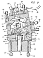
- FIG. 9 A general layout of another embodiment is shown in Figure 9 .
- the microscope is compact, formed from an aluminum block housing 140 carried on a base plate 142 which has a central opening 144.
- the housing 140 defines a cavity 146 in which is disposed a cantilever module 148.
- the module 148 is formed with a medial opening 150 in which a lower lens 152 and upper lens assembly 154 are fixed above a cantilever 156 carried on a cantilever chip 158 which is secured to the bottom of the module 148.
- the housing 140 supports a movable lens 160 carried by a lens holder 162 which is movable against a spring 164 by a bolt 166 threadably carried in a bolthole 168 in the block 140 and turned against the bias of the spring 164 by a focus knob 170.
- a polarizing beam splitter 172, above and integral with a quarterwave plate 174 is supported in the path of the light between movable lens 160 and the upper lens assembly 154.
- the beamsplitter 176 is supported on a tiltstage 182 which includes two adjustment screws 184 and 186 and a pivot point (not shown).
- Light from an optical fiber 188 goes through a collimator 190 to be directed by the incident light beamsplitter 176 through openings 192 and 194, respectively, in the tiltstage 182 and block 140.
- the forward end of the collimator 190 abuts a slit 191 into what can be placed on a plate having an aperture opening shaped as desired.
- the tiltstage 182 positions the focused spot on the cantilever 156.
- Collimated light from the incident beam splitter 176 travels through the movable lens 160, polarizing beam splitter 172, quarterwave plate 174 and fixed lenses 154 and 152 to impinge on the top side of the cantilever 156.
- Light reflected from the cantilever travels back through the fixed lenses 152 and 154, through the quarterwave plate 174 and is reflected by the beamsplitter 172.
- a detector 196 is positioned in the block cavity 146 and is carried by an arm 198 connected to a detector tiltstage 200 which, by means of adjustment screws two of which, 202 and 204, are shown, centers the reflected beam onto the detector 196.
- the cantilever module 148 is carried on the base plate 142 by a steel ball 206 on one side and by a steel hemisphere 208 on the other side, and which are located by cavities, respectively 210 and 212 formed in the bottom of the cantilever module 148.
- the steel hemisphere 208 is glued to a z-directional tapping piezoelectric actuator 214 which has wires (not shown) leading to a control (not shown) to enable a tapping mode to the cantilever operation. While such placement of the tapping piezoelectric actuator 214 simplifies construction of the device and can replace the piezoelectric tapping actuator and can be placed in other locations, for example, in the fluid cell. Alternatively, a piezoelectric actuator can be located and each ball supporting the cantilever module.
- the sample 216 is supported on a piezoelectric scan tube 218 carried in a scanner assembly 220.
- the scan tube 218 is of conventional design well-known in the art whereby application of x-, y-, and z-directional voltages over wires (not shown) moves the sample horizontally and vertically.
- the base plate 142 is supported on the scanner assembly 220 by means of locating cavities 222 and 224 which interface with steel balls, respectively, 226 and 228 carried on adjustment screws, respectively, 230 and 232.
Landscapes
- Nuclear Medicine, Radiotherapy & Molecular Imaging (AREA)
- General Health & Medical Sciences (AREA)
- General Physics & Mathematics (AREA)
- Health & Medical Sciences (AREA)
- Radiology & Medical Imaging (AREA)
- Physics & Mathematics (AREA)
- Chemical & Material Sciences (AREA)
- Nanotechnology (AREA)
- Engineering & Computer Science (AREA)
- Analytical Chemistry (AREA)
- Crystallography & Structural Chemistry (AREA)
- Length Measuring Devices By Optical Means (AREA)
- Microscoopes, Condenser (AREA)
- Measurement Of Length, Angles, Or The Like Using Electric Or Magnetic Means (AREA)
- Length Measuring Devices With Unspecified Measuring Means (AREA)
Claims (18)
- Rasterkraftmikroskop mit
zumindest einem Mikroskopbalken (14; 156), der in dem Rasterkraftmikroskop angebracht ist;
einem optischen Detektor (46; 196);
einem optischen System mit einer Lichtquelle (32) und einer Einrichtung (24, 34, 38; 60, 62; 94; 152, 154, 160) zum Erzeugen eines fokussierten einfallenden Strahls (44, 44a) von Licht, der aus einem einzelnen Strahl besteht, der den einfallenden Strahl bildet, und zum Ausrichten des fokussierten einfallenden Strahls (44, 44a) auf den Mikroskopbalken (14; 156); und
einer Einrichtung (40, 42; 172, 174) zum vollständigen Ausrichten des von dem Mikroskopbalken (14; 156) reflektierten Strahls auf den Detektor (46; 196), wobei die Komponenten des optischen Systems so angeordnet sind, dass zumindest Abschnitte der einfallenden und reflektierten Strahlen überlappen und sie eine Einrichtung zum Trennen des reflektierten Strahls von dem einfallenden Strahl und zum Ausrichten des getrennten reflektierten Strahls auf den Detektor (46, 196) enthält,
dadurch gekennzeichnet, dass
das optische System eine numerische Apertur hat, die ausreichend ist, um mit der Wellenlänge des fokussierten einfallenden Strahls (44, 44a) einen Einfallsstrahlfleck auf den Mikroskopbalken (14; 156) mit einer Größe von 8 µm oder weniger in zumindest einer Dimension zu bilden, und dass es ferner eine Einrichtung (62, 70, 82; 94, 98, 100, 102) zum Anordnen der Fokusebene des einfallenden Strahls (44, 44a) auf die Ebene des Mikroskopbalkens (14, 10, 156) aufweist, wobei die Fokusebenenanordnungseinrichtung zumindest eines von einer Fokuslinse (94), die angeordnet ist, den einfallenden Strahl (44, 44a) auf den Mikroskopbalken (14) zu fokussieren, und einer Einrichtung (98, 100, 102) zum Neigen der Fokuslinse (94) aufweist, bis ihre Fokusebene auf der Ebene des Mikroskopbalkens (14) ist. - Rasterkraftmikroskop nach Anspruch 1, wobei der Mikroskopbalken (14; 156) eine Länge von weniger als 30 µm hat.
- Rasterkraftmikroskop nach Anspruch 1 oder 2, ferner mit einer Einrichtung zum Definieren einer Apertur (34) in dem Pfad des einfallenden Strahls (44, 44a) und einer Einrichtung (39) zum Anpassen der Größe der Apertur (34), wodurch die Größe des Einfallsstrahlflecks auf dem Mikroskopbalken (14; 156) gesteuert wird.
- Rasterkraftmikroskop nach Anspruch 1 oder 2, ferner mit einer Einrichtung zum Definieren einer Apertur (34) in dem Pfad des einfallenden Strahls (44, 44a) und einer Einrichtung zum Anpassen der Form der Apertur (34), wodurch die Form des Einfallsstrahlflecks auf dem Mikroskopbalken (14; 156) gesteuert wird.
- Rasterkraftmikroskop nach Anspruch 4, wobei die Trenneinrichtung einen Polarisationsstrahlteiler (40; 172) in dem Pfad des einfallenden Strahls (44, 44a) und des reflektierten Strahls, der angebracht ist, Licht einer ersten Polarisationsrichtung durchzulassen und Licht einer zweiten Polarisationsrichtung zu reflektieren, und eine Umwandlungseinrichtung (42; 174) aufweist, die zwischen dem Strahlteiler (40; 172) und dem Mikroskopbalken (14; 156) in dem Pfad der überlappenden Strahlen lokalisiert ist, um zumindest einen Teil des reflektierten Strahls in die zweite Polarisationsrichtung umzuwandeln.
- Rasterkraftmikroskop nach Anspruch 5, wobei die Umwandlungseinrichtung eine Viertelwellenplatte (42; 174) aufweist, die den einfallenden Strahl (44, 44a) elliptisch polarisiert und den reflektierten Strahl linear polarisiert.
- Rasterkraftmikroskop nach Anspruch 1, ferner mit einem Polarisierer in dem Pfad des einfallenden Strahls (44, 44a), aber außerhalb des Pfads der überlappenden Strahlen, der angeordnet ist, Licht mit im Wesentlichen nur einer Polarisationsrichtung durchzulassen, wobei die Trenneinrichtung einen Strahlteiler (40; 172) in dem Pfad des einfallenden Strahls (44, 44a) und des reflektierten Strahls aufweist, der angeordnet ist, Licht mit einer ersten Polarisationsrichtung durchzulassen und Licht mit einer zweiten Polarisationsrichtung zu reflektieren, und einer Umwandlungseinrichtung (42; 174) zum Umwandeln von zumindest einem Teil des reflektierten Lichtstrahls in die zweite Polarisationsrichtung, die zwischen dem Strahlteiler (40; 172) und dem Mikroskopbalken (14; 156) in dem Pfad der überlappenden Strahlen lokalisiert ist.
- Rasterkraftmikroskop nach Anspruch 7, wobei die Umwandlungseinrichtung eine Viertelwellenplatte (42; 174) aufweist, die den einfallenden Strahl (44, 44a) elliptisch polarisiert und den reflektierten Strahl linear polarisiert.
- Rasterkraftmikroskop nach einem der Ansprüche 1 bis 8, mit einer Sichteinrichtung (38; 160), die konfokal mit der Linse (24; 60; 94; 152, 154) ist, um den Ort des Einfallsstrahlflecks zu sehen.
- Rasterkraftmikroskop nach Anspruch 9, wobei sich zumindest Teile des einfallenden Strahls (44, 44a) und des reflektierten Strahls und der Sichteinrichtung (38; 160) einen gemeinsamen optischen Pfad teilen.
- Rasterkraftmikroskop nach Anspruch 10, wobei die Lichtquelle (32) eine Quelle kollimierten Lichts ist, und die Optik der Sichteinrichtung auf unendlich korrigiert ist.
- Rasterkraftmikroskop nach Anspruch 10 oder 11, wobei die Sichteinrichtung eine verlagerbare Linse (38, 160) in dem gemeinsamen optischen Pfad enthält, wodurch ihre Verlagerung, um das Bild des Mikroskopbalkens (14; 156) in der Sichteinrichtung zu fokussieren, darin resultiert, dass der Einfallsstrahl (44, 44a) in der Ebene des Mikroskopbalkens (14; 156) fokussiert wird.
- Rasterkraftmikroskop nach Anspruch 1, wobei die Fokusebenenanordnungseinrichtung zumindest eine Fokuslinse aufweist, die angeordnet ist, den einfallenden Strahl (44, 44a) auf dem Mikroskopbalken (14) zu fokussieren, wobei ihre optische Achse so angeordnet ist, dass sie senkrecht zu der Ebene des Mikroskoparms (14) ist.
- Rasterkraftmikroskop nach einem der Ansprüche 1 bis 13 mit einer Vielzahl von Mikroskoparmen (14i bis 14iv), einer Einrichtung zum Verschieben des Fokusflecks des einfallenden Strahls (44, 44a) von einem Mikroskopbalken zu einem anderen, und einer Einrichtung zum Anordnen der Fokusebene des einfallenden Strahls (44, 44a) auf der Ebene von zumindest einem der Vielzahl von Mikroskopbalken (14i bis 14iv), wodurch der einfallende Strahl (44, 44a) im Wesentlichen auf den Mikroskopbalken fokussiert ist, auf den der Fokusfleck verschoben wurde.
- Rasterkraftmikroskop nach einem der Ansprüche 1 bis 14, ferner mit einem entfernbar angebrachten Modul (10; 76; 114; 148), an das der Mikroskopbalken (14; 156) montiert ist, wobei eine oder die Fokuslinse (24; 60; 94; 154) zum Fokussieren des einfallenden Strahls (44, 44a) auf den Einfallsstrahlfleck auf dem Mikroskopbalken (14; 56) an dem Modul montiert ist.
- Rasterkraftmikroskop nach Anspruch 15, ferner mit zumindest einem piezoelektrischen Intermittentelement (214), von dem das Modul (148) getragen wird, um den Intermittent-Modus-Betrieb zu erleichtern.
- Rasterkraftmikroskop nach Anspruch 16, wobei das Modul (148) an einem Träger (142) angeordnet ist, in dem das piezoelektrische Intermittentelement (214) eingebettet ist.
- Rasterkraftmikroskop nach einem der Ansprüche 1 bis 17, wobei die Wellenlänge des Lichts von der Lichtquelle (32) 670 nm beträgt und die numerische Apertur größer als 0,05 ist.
Applications Claiming Priority (2)
| Application Number | Priority Date | Filing Date | Title |
|---|---|---|---|
| US08/709,349 US5825020A (en) | 1996-09-06 | 1996-09-06 | Atomic force microscope for generating a small incident beam spot |
| EP97938447A EP1012862B1 (de) | 1996-09-06 | 1997-08-20 | Rasterkraftmikroskop zur erzeugung eines kleinen einfallsstrahlflecks |
Related Parent Applications (1)
| Application Number | Title | Priority Date | Filing Date |
|---|---|---|---|
| EP97938447A Division EP1012862B1 (de) | 1996-09-06 | 1997-08-20 | Rasterkraftmikroskop zur erzeugung eines kleinen einfallsstrahlflecks |
Publications (3)
| Publication Number | Publication Date |
|---|---|
| EP1892499A2 EP1892499A2 (de) | 2008-02-27 |
| EP1892499A3 EP1892499A3 (de) | 2010-01-27 |
| EP1892499B1 true EP1892499B1 (de) | 2014-03-19 |
Family
ID=24849492
Family Applications (2)
| Application Number | Title | Priority Date | Filing Date |
|---|---|---|---|
| EP07121018.1A Expired - Lifetime EP1892499B1 (de) | 1996-09-06 | 1997-08-20 | Atomkraftmikroskop zur Erzeugung eines kleinen Ereignisstrahlenpunktes |
| EP97938447A Expired - Lifetime EP1012862B1 (de) | 1996-09-06 | 1997-08-20 | Rasterkraftmikroskop zur erzeugung eines kleinen einfallsstrahlflecks |
Family Applications After (1)
| Application Number | Title | Priority Date | Filing Date |
|---|---|---|---|
| EP97938447A Expired - Lifetime EP1012862B1 (de) | 1996-09-06 | 1997-08-20 | Rasterkraftmikroskop zur erzeugung eines kleinen einfallsstrahlflecks |
Country Status (7)
| Country | Link |
|---|---|
| US (1) | US5825020A (de) |
| EP (2) | EP1892499B1 (de) |
| JP (1) | JP2000517433A (de) |
| AU (1) | AU4076797A (de) |
| CA (1) | CA2264747A1 (de) |
| DE (1) | DE69738317T2 (de) |
| WO (1) | WO1998010458A1 (de) |
Families Citing this family (37)
| Publication number | Priority date | Publication date | Assignee | Title |
|---|---|---|---|---|
| US6490913B1 (en) | 1995-05-19 | 2002-12-10 | The United States Of America As Represented By The Secretary Of Commerce | Humidity chamber for scanning stylus atomic force microscope with cantilever tracking |
| US6200022B1 (en) * | 1997-04-21 | 2001-03-13 | Ta Instruments, Inc. | Method and apparatus for localized dynamic mechano-thermal analysis with scanning probe microscopy |
| JP3497734B2 (ja) * | 1997-07-24 | 2004-02-16 | オリンパス株式会社 | 走査型プローブ顕微鏡 |
| US6123819A (en) | 1997-11-12 | 2000-09-26 | Protiveris, Inc. | Nanoelectrode arrays |
| US6455838B2 (en) * | 1998-10-06 | 2002-09-24 | The Regents Of The University Of California | High sensitivity deflection sensing device |
| JP3995819B2 (ja) * | 1999-01-18 | 2007-10-24 | エスアイアイ・ナノテクノロジー株式会社 | 走査型プローブ顕微鏡 |
| DE19957418B4 (de) * | 1999-11-29 | 2016-02-04 | Leica Microsystems Cms Gmbh | Verfahren zur lichtoptischen Abtastung eines Objekts und Rastermikroskop zur Anwendung des Verfahrens |
| DE10297054T5 (de) * | 2001-07-18 | 2004-10-14 | The Regents Of The University Of California, Oakland | Messkopf für ein Rasterkraftmikroskop und weitere Anwendungen |
| US6884981B2 (en) * | 2001-08-23 | 2005-04-26 | Asylum Research Corp. | Diffractive optical position detector |
| EP1430486B1 (de) * | 2001-09-24 | 2007-10-31 | JPK Instruments AG | Verfahren und vorrichtung zum messen einer probe mit hilfe eines rastersondenmikroskops |
| US6718821B1 (en) | 2001-11-07 | 2004-04-13 | Sandia Corporation | Laser interferometry force-feedback sensor for an interfacial force microscope |
| US7687767B2 (en) * | 2002-12-20 | 2010-03-30 | Agilent Technologies, Inc. | Fast scanning stage for a scanning probe microscope |
| JPWO2005015570A1 (ja) * | 2003-08-11 | 2007-11-22 | 独立行政法人科学技術振興機構 | 透明基板を用いるプローブ顕微鏡のプローブ、その製造方法およびプローブ顕微鏡装置 |
| US7278298B2 (en) * | 2004-11-30 | 2007-10-09 | The Regents Of The University Of California | Scanner for probe microscopy |
| US7249494B2 (en) * | 2005-06-06 | 2007-07-31 | Academia Sinica | Beam tracking system for scanning-probe type atomic force microscope |
| JP4810251B2 (ja) * | 2006-02-16 | 2011-11-09 | キヤノン株式会社 | 原子間力顕微鏡 |
| DE112007001927B4 (de) * | 2006-08-18 | 2016-07-07 | Jpk Instruments Ag | Vorrichtung und Verfahren zum sondermikroskopischen Untersuchen einer Probe |
| US7692138B1 (en) | 2006-10-23 | 2010-04-06 | David James Ray | Integrated scanning probe microscope and confocal microscope |
| US8166567B2 (en) * | 2007-03-16 | 2012-04-24 | Bruker Nano, Inc. | Fast-scanning SPM scanner and method of operating same |
| US8156568B2 (en) * | 2007-04-27 | 2012-04-10 | Picocal, Inc. | Hybrid contact mode scanning cantilever system |
| DE102007033441B4 (de) * | 2007-07-18 | 2013-04-18 | SIOS Meßtechnik GmbH | Vorrichtung zur gleichzeitigen Messung von Kräften |
| US7759631B2 (en) | 2008-01-22 | 2010-07-20 | Nanosurf Ag | Raster scanning microscope having transparent optical element with inner curved surface |
| AU2009273838A1 (en) * | 2008-07-25 | 2010-01-28 | Oregon Health & Science University | Rapid confocal microscopy to support surgical procedures |
| US20140223612A1 (en) * | 2013-02-05 | 2014-08-07 | Asylum Corporation | Modular Atomic Force Microscope |
| JP5232681B2 (ja) * | 2009-02-16 | 2013-07-10 | 日本電子株式会社 | 走査プローブ顕微鏡及びその動作方法 |
| US8667611B2 (en) * | 2010-04-29 | 2014-03-04 | The Royal Institution For The Advancement Of Learning/Mcgill University | Method and apparatus for measuring cantilever deflection in constrained spaces |
| DE102010026171A1 (de) * | 2010-07-06 | 2012-01-12 | Carl Zeiss Surgical Gmbh | Digitales Mikroskopiesystem |
| JP5913818B2 (ja) * | 2011-03-07 | 2016-04-27 | オリンパス株式会社 | 走査機構および走査型プローブ顕微鏡 |
| JP2013113727A (ja) * | 2011-11-29 | 2013-06-10 | Hitachi High-Technologies Corp | ヘッド素子検査機 |
| WO2013150624A1 (ja) * | 2012-04-04 | 2013-10-10 | オリンパス株式会社 | 走査機構および走査型プローブ顕微鏡 |
| US9383386B2 (en) | 2013-03-14 | 2016-07-05 | Oxford Instruments Asylum Research, Inc. | Optical beam positioning unit for atomic force microscope |
| US9097737B2 (en) | 2013-11-25 | 2015-08-04 | Oxford Instruments Asylum Research, Inc. | Modular atomic force microscope with environmental controls |
| US9804193B2 (en) | 2014-03-12 | 2017-10-31 | Oxford Instruments Asylum Research, Inc | Metrological scanning probe microscope |
| US10705114B2 (en) | 2014-03-12 | 2020-07-07 | Oxford Instruments Asylum Research Inc | Metrological scanning probe microscope |
| AT517809B1 (de) | 2015-08-19 | 2017-11-15 | Anton Paar Gmbh | Mit Masterkraft werkzeuglos betätigbarer und eine Messsonde lösbar fixierender Fixiermechanismus für Rastersondenmikroskop |
| WO2018109803A1 (ja) * | 2016-12-12 | 2018-06-21 | オリンパス株式会社 | 原子間力顕微鏡 |
| US11519935B2 (en) * | 2020-08-18 | 2022-12-06 | Oxford Instruments Asylum Research, Inc. | Atomic force microscope |
Family Cites Families (18)
| Publication number | Priority date | Publication date | Assignee | Title |
|---|---|---|---|---|
| DE3856575T2 (de) * | 1987-08-12 | 2005-11-10 | Olympus Optical Co., Ltd. | Rastertunnelmikroskop |
| US4935634A (en) * | 1989-03-13 | 1990-06-19 | The Regents Of The University Of California | Atomic force microscope with optional replaceable fluid cell |
| US5260824A (en) * | 1989-04-24 | 1993-11-09 | Olympus Optical Co., Ltd. | Atomic force microscope |
| US5017010A (en) * | 1989-05-16 | 1991-05-21 | International Business Machines Corporation | High sensitivity position sensor and method |
| US5206702A (en) * | 1989-10-09 | 1993-04-27 | Olympus Optical Co., Ltd. | Technique for canceling the effect of external vibration on an atomic force microscope |
| JP2679339B2 (ja) * | 1990-03-07 | 1997-11-19 | 松下電器産業株式会社 | 微小変位検出装置 |
| US5394741A (en) * | 1990-07-11 | 1995-03-07 | Olympus Optical Co., Ltd. | Atomic probe microscope |
| US5231286A (en) * | 1990-08-31 | 1993-07-27 | Olympus Optical Co., Ltd. | Scanning probe microscope utilizing an optical element in a waveguide for dividing the center part of the laser beam perpendicular to the waveguide |
| US5144833A (en) * | 1990-09-27 | 1992-09-08 | International Business Machines Corporation | Atomic force microscopy |
| US5157251A (en) | 1991-03-13 | 1992-10-20 | Park Scientific Instruments | Scanning force microscope having aligning and adjusting means |
| US5172002A (en) * | 1991-08-22 | 1992-12-15 | Wyko Corporation | Optical position sensor for scanning probe microscopes |
| US5298975A (en) * | 1991-09-27 | 1994-03-29 | International Business Machines Corporation | Combined scanning force microscope and optical metrology tool |
| US5291775A (en) * | 1992-03-04 | 1994-03-08 | Topometrix | Scanning force microscope with integrated optics and cantilever mount |
| US5672816A (en) * | 1992-03-13 | 1997-09-30 | Park Scientific Instruments | Large stage system for scanning probe microscopes and other instruments |
| US5463897A (en) * | 1993-08-17 | 1995-11-07 | Digital Instruments, Inc. | Scanning stylus atomic force microscope with cantilever tracking and optical access |
| US5388452A (en) * | 1993-10-15 | 1995-02-14 | Quesant Instrument Corporation | Detection system for atomic force microscopes |
| JP3425615B2 (ja) * | 1994-03-24 | 2003-07-14 | 科学技術庁長官官房会計課長 | 走査型近視野原子間力顕微鏡 |
| JP3174465B2 (ja) * | 1994-11-28 | 2001-06-11 | 松下電器産業株式会社 | 原子間力顕微鏡 |
-
1996
- 1996-09-06 US US08/709,349 patent/US5825020A/en not_active Expired - Lifetime
-
1997
- 1997-08-20 EP EP07121018.1A patent/EP1892499B1/de not_active Expired - Lifetime
- 1997-08-20 AU AU40767/97A patent/AU4076797A/en not_active Abandoned
- 1997-08-20 WO PCT/US1997/014622 patent/WO1998010458A1/en not_active Ceased
- 1997-08-20 CA CA002264747A patent/CA2264747A1/en not_active Abandoned
- 1997-08-20 EP EP97938447A patent/EP1012862B1/de not_active Expired - Lifetime
- 1997-08-20 DE DE69738317T patent/DE69738317T2/de not_active Expired - Lifetime
- 1997-08-20 JP JP10512687A patent/JP2000517433A/ja active Pending
Also Published As
| Publication number | Publication date |
|---|---|
| JP2000517433A (ja) | 2000-12-26 |
| EP1892499A2 (de) | 2008-02-27 |
| DE69738317T2 (de) | 2008-10-02 |
| CA2264747A1 (en) | 1998-03-12 |
| US5825020A (en) | 1998-10-20 |
| EP1012862B1 (de) | 2007-11-21 |
| EP1012862A4 (de) | 2001-03-28 |
| EP1892499A3 (de) | 2010-01-27 |
| EP1012862A1 (de) | 2000-06-28 |
| AU4076797A (en) | 1998-03-26 |
| DE69738317D1 (de) | 2008-01-03 |
| WO1998010458A1 (en) | 1998-03-12 |
Similar Documents
| Publication | Publication Date | Title |
|---|---|---|
| EP1892499B1 (de) | Atomkraftmikroskop zur Erzeugung eines kleinen Ereignisstrahlenpunktes | |
| KR100192097B1 (ko) | 원자간력현미경 | |
| EP0640829B1 (de) | Rastertunnelmikroskop | |
| US6181474B1 (en) | Scanning confocal microscope with objective lens position tracking | |
| US7738113B1 (en) | Wafer measurement system and apparatus | |
| US6144028A (en) | Scanning probe microscope assembly and method for making confocal, spectrophotometric, Near-Field, and Scanning probe measurements and associated images | |
| US5859364A (en) | Scanning probe microscope | |
| JP2002512697A (ja) | 固体界浸レンズを用いた走査プローブ光学顕微鏡 | |
| US5739527A (en) | Near-field optical microscope for angle resolved measurements | |
| JPH05256641A (ja) | カンチレバー変位検出装置 | |
| US10054612B2 (en) | Optical beam positioning unit for atomic force microscope | |
| KR20060124786A (ko) | 광섬유 탐침, 광검출 장치, 및 광검출 방법 | |
| JPH07128595A (ja) | 光学顕微鏡を用いて緻密なライン幅構造を映像化する方法及び装置 | |
| JP2791121B2 (ja) | 微細表面形状計測装置 | |
| JPH09105865A (ja) | 走査型近接場光学顕微鏡 | |
| JP2008134190A (ja) | カンチレバーホルダーおよびこれを備えた走査型プローブ顕微鏡 | |
| JP4262621B2 (ja) | 原子間力顕微鏡 | |
| JP2833631B2 (ja) | 近視野光学顕微鏡 | |
| JPH0972924A (ja) | 走査型プローブ顕微鏡 | |
| JP2000234994A (ja) | 走査プローブ顕微鏡におけるカンチレバー変位測定方法 | |
| JPH0626853A (ja) | 原子間力顕微鏡 | |
| JPH08220114A (ja) | 走査型力顕微鏡の変位検出装置 | |
| JP4500033B2 (ja) | 近接場光学顕微鏡 | |
| JPH05312561A (ja) | 原子間力顕微鏡 | |
| JPH1073605A (ja) | カンチレバー変位検出装置 |
Legal Events
| Date | Code | Title | Description |
|---|---|---|---|
| PUAI | Public reference made under article 153(3) epc to a published international application that has entered the european phase |
Free format text: ORIGINAL CODE: 0009012 |
|
| AC | Divisional application: reference to earlier application |
Ref document number: 1012862 Country of ref document: EP Kind code of ref document: P |
|
| AK | Designated contracting states |
Kind code of ref document: A2 Designated state(s): AT BE BG CH CY CZ DE DK EE ES FI FR GB GR HU IE IS IT LI LT LU LV MC MT NL PL PT RO SE SI SK TR |
|
| AX | Request for extension of the european patent |
Extension state: AL BA HR MK YU |
|
| PUAL | Search report despatched |
Free format text: ORIGINAL CODE: 0009013 |
|
| AK | Designated contracting states |
Kind code of ref document: A3 Designated state(s): AT BE BG CH CY CZ DE DK EE ES FI FR GB GR HU IE IS IT LI LT LU LV MC MT NL PL PT RO SE SI SK TR |
|
| AX | Request for extension of the european patent |
Extension state: AL BA HR MK RS |
|
| RIC1 | Information provided on ipc code assigned before grant |
Ipc: G01B 7/34 20060101AFI20080123BHEP Ipc: H01J 3/14 20060101ALI20091223BHEP |
|
| 17P | Request for examination filed |
Effective date: 20100303 |
|
| 17Q | First examination report despatched |
Effective date: 20100330 |
|
| AKX | Designation fees paid |
Designated state(s): DE FR GB |
|
| RIC1 | Information provided on ipc code assigned before grant |
Ipc: G01Q 70/06 20100101ALI20130712BHEP Ipc: H01J 3/14 20060101ALI20130712BHEP Ipc: G01B 7/34 20060101AFI20130712BHEP Ipc: G01Q 60/38 20100101ALI20130712BHEP Ipc: G01Q 20/02 20100101ALI20130712BHEP Ipc: B82Y 35/00 20110101ALI20130712BHEP |
|
| GRAP | Despatch of communication of intention to grant a patent |
Free format text: ORIGINAL CODE: EPIDOSNIGR1 |
|
| INTG | Intention to grant announced |
Effective date: 20131009 |
|
| GRAS | Grant fee paid |
Free format text: ORIGINAL CODE: EPIDOSNIGR3 |
|
| GRAA | (expected) grant |
Free format text: ORIGINAL CODE: 0009210 |
|
| AC | Divisional application: reference to earlier application |
Ref document number: 1012862 Country of ref document: EP Kind code of ref document: P |
|
| AK | Designated contracting states |
Kind code of ref document: B1 Designated state(s): DE FR GB |
|
| REG | Reference to a national code |
Ref country code: GB Ref legal event code: FG4D |
|
| REG | Reference to a national code |
Ref country code: DE Ref legal event code: R096 Ref document number: 69740701 Country of ref document: DE Effective date: 20140430 |
|
| REG | Reference to a national code |
Ref country code: DE Ref legal event code: R097 Ref document number: 69740701 Country of ref document: DE |
|
| PLBE | No opposition filed within time limit |
Free format text: ORIGINAL CODE: 0009261 |
|
| STAA | Information on the status of an ep patent application or granted ep patent |
Free format text: STATUS: NO OPPOSITION FILED WITHIN TIME LIMIT |
|
| 26N | No opposition filed |
Effective date: 20141222 |
|
| REG | Reference to a national code |
Ref country code: DE Ref legal event code: R097 Ref document number: 69740701 Country of ref document: DE Effective date: 20141222 |
|
| REG | Reference to a national code |
Ref country code: FR Ref legal event code: PLFP Year of fee payment: 20 |
|
| PGFP | Annual fee paid to national office [announced via postgrant information from national office to epo] |
Ref country code: GB Payment date: 20160824 Year of fee payment: 20 |
|
| PGFP | Annual fee paid to national office [announced via postgrant information from national office to epo] |
Ref country code: FR Payment date: 20160829 Year of fee payment: 20 |
|
| PGFP | Annual fee paid to national office [announced via postgrant information from national office to epo] |
Ref country code: DE Payment date: 20161012 Year of fee payment: 20 |
|
| REG | Reference to a national code |
Ref country code: DE Ref legal event code: R071 Ref document number: 69740701 Country of ref document: DE |
|
| REG | Reference to a national code |
Ref country code: GB Ref legal event code: PE20 Expiry date: 20170819 |
|
| PG25 | Lapsed in a contracting state [announced via postgrant information from national office to epo] |
Ref country code: GB Free format text: LAPSE BECAUSE OF EXPIRATION OF PROTECTION Effective date: 20170819 |