EP1860767A2 - Halbleitervorrichtung für eine Motoransteuerung und Motor damit, Motoransteuerungsvorrichtung und Luftkühlanlage - Google Patents
Halbleitervorrichtung für eine Motoransteuerung und Motor damit, Motoransteuerungsvorrichtung und Luftkühlanlage Download PDFInfo
- Publication number
- EP1860767A2 EP1860767A2 EP07010278A EP07010278A EP1860767A2 EP 1860767 A2 EP1860767 A2 EP 1860767A2 EP 07010278 A EP07010278 A EP 07010278A EP 07010278 A EP07010278 A EP 07010278A EP 1860767 A2 EP1860767 A2 EP 1860767A2
- Authority
- EP
- European Patent Office
- Prior art keywords
- dead time
- motor
- semiconductor device
- heat exchanger
- driving
- Prior art date
- Legal status (The legal status is an assumption and is not a legal conclusion. Google has not performed a legal analysis and makes no representation as to the accuracy of the status listed.)
- Granted
Links
Images






Classifications
-
- H—ELECTRICITY
- H02—GENERATION; CONVERSION OR DISTRIBUTION OF ELECTRIC POWER
- H02M—APPARATUS FOR CONVERSION BETWEEN AC AND AC, BETWEEN AC AND DC, OR BETWEEN DC AND DC, AND FOR USE WITH MAINS OR SIMILAR POWER SUPPLY SYSTEMS; CONVERSION OF DC OR AC INPUT POWER INTO SURGE OUTPUT POWER; CONTROL OR REGULATION THEREOF
- H02M7/00—Conversion of AC power input into DC power output; Conversion of DC power input into AC power output
- H02M7/003—Constructional details, e.g. physical layout, assembly, wiring or busbar connections
-
- H—ELECTRICITY
- H02—GENERATION; CONVERSION OR DISTRIBUTION OF ELECTRIC POWER
- H02M—APPARATUS FOR CONVERSION BETWEEN AC AND AC, BETWEEN AC AND DC, OR BETWEEN DC AND DC, AND FOR USE WITH MAINS OR SIMILAR POWER SUPPLY SYSTEMS; CONVERSION OF DC OR AC INPUT POWER INTO SURGE OUTPUT POWER; CONTROL OR REGULATION THEREOF
- H02M1/00—Details of apparatus for conversion
- H02M1/38—Means for preventing simultaneous conduction of switches
-
- H—ELECTRICITY
- H02—GENERATION; CONVERSION OR DISTRIBUTION OF ELECTRIC POWER
- H02P—CONTROL OR REGULATION OF ELECTRIC MOTORS, ELECTRIC GENERATORS OR DYNAMO-ELECTRIC CONVERTERS; CONTROLLING TRANSFORMERS, REACTORS OR CHOKE COILS
- H02P25/00—Arrangements or methods for the control of AC motors characterised by the kind of AC motor or by structural details
- H02P25/02—Arrangements or methods for the control of AC motors characterised by the kind of AC motor or by structural details characterised by the kind of motor
- H02P25/022—Synchronous motors
- H02P25/03—Synchronous motors with brushless excitation
Definitions
- the present invention relates to a semiconductor device for motor driving and a motor having the semiconductor device, a motor driving apparatus and an air conditioner.
- Inverter-controlled three-phase brushless motors are widely adopted recently as motors of electrical household appliances and industrial machines. Price competition is severe particularly for electrical household appliances. It is desired to supply inexpensive inverters.
- a 120-degree rectangular wave driving method is therefore adopted as an inverter operation method, because this driving method uses a relatively simple circuit structure, can increase a motor efficiency and provide an inexpensive inverter.
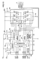
- reference numeral 1 represents a commercial power source and reference numeral 2 represents a power source circuit.
- VDC, Vcc and Vm are generated from AC voltage of the commercial power source 1.
- VDC is a main power supply voltage for inverter motor drive
- Vcc is a power supply voltage for driving circuits in a semiconductor device 100 which drives a 120-degree rectangular wave driving type motor
- Vm is a power supply voltage for a microcomputer 3.
- the microcomputer 3 outputs a speed command signal Vsp to a motor 50 and receives a speed signal FG from the motor 50.
- the power source circuit 2 and microcomputer 3 are mounted on a first board 4.
- the motor 50 has a board 60 built in the motor.
- the semiconductor device 100 for driving the 120-degree rectangular wave driving type motor, a Hall IC 90 and a shunt resistor Rs are disposed on the board 60 built in the motor.
- Coils 8 are connected to output terminals of the semiconductor device 100 for driving the 120-degree rectangular wave driving type motor.
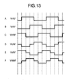
- Fig. 13 is a timing chart illustrating the 120-degree rectangular wave driving method.
- a to C in Fig. 13 indicate magnetic pole position signals VHU', VHV' and VHW'
- D to F in Fig. 13 indicate the outline of waveforms of output voltages VUM', VVM' and VWM'.
- the semiconductor device 100 for driving the 120-degree rectangular wave driving type motor outputs an H signal and an L signal each having a 120-degree electrical angle period, in accordance with the magnetic pole position signals VHU', VHV' and VHW'. Current flows through the coils 8 during the 120-degree period, and a non-feeding period of 60 degrees exist between respective 120-degree periods. As the motor is driven by the 120-degree rectangular wave driving method, torque ripples of the motor become large so that noises are likely to be generated during motor driving.
- Patent Document 1 JP-A-2004-120841 discloses a method of changing a phase current to a quasi sine waveform with low cost by using analog circuits.
- Another method of reducing noises of a motor is a method called a sine wave driving method which changes a phase current of the motor to a sine waveform.
- a sine wave driving method which changes a phase current of the motor to a sine waveform.
- High performance and low price of a microcomputer is advancing nowadays, and the sine wave driving method using a microcomputer is an optimum method of reducing noises of a motor.
- Patent Document 1 JP-A-2004-120841
- a controlling semiconductor device such as a microcomputer has generally a lower resistance against noises and the like than a semiconductor device for driving a motor, and is likely to have a malfunction. If the controlling semiconductor device enters an abnormal state during noise superposition or the like and outputs an abnormal control signal, there is a possibility that the semiconductor device for driving the motor has upper and lower electrical shortage and is broken.
- a device particularly a microcomputer
- the semiconductor device for driving the motor is broken during a period until a watch dog timer operates after the microcomputer runs away. Further, even while the controlling semiconductor device outputs a normal control signal, there is a possibility that the semiconductor device for driving the motor is broken because of upper and lower electrical shortage, when noises are superposed on a wiring interconnecting the controlling semiconductor device and the semiconductor device for driving the motor or in other cases.
- a motor driving semiconductor device comprising: six switching elements for driving a three-phase motor; three output terminals for applying output voltages to three terminals of coils of the three-phase motor; drive circuits for driving the six switching elements; and six control signal input terminals for receiving six control signals for on/off control of the six switching elements, wherein the motor driving semiconductor device is formed by sealing at least one semiconductor chip in one package with resin, and further comprises a dead time generation function of generating a dead time relative to the six control signals.
- the present invention it is possible to reduce torque ripples of a motor without lowering reliability, in a sine wave driving method using a controlling semiconductor device such as a microcomputer. Even if the controlling semiconductor device enters an abnormal state or noises are superposed on a control signal, the semiconductor device for driving the motor will not be broken so that the controlling semiconductor device and the semiconductor device for controlling the motor can be disposed in an environment having large noises such as the inside of a housing of the motor.
- the present invention provides the advantages of preventing breakage to be caused by upper and lower through conduction and obtaining high reliability in the application fields other than the sine wave driving method using a controlling semiconductor device such as a microcomputer.
- the advantages of preventing breakage to be caused by upper and lower through conduction and obtaining high reliability are also presented to, for example, a quasi sine wave driving method, a 150-degree driving method, a broad angle control method and an overlap control method. Any control method can have the advantages of preventing breakage to be caused by upper and lower through conduction and obtaining high reliability, irrespective of the types of control methods.
- Fig. 1 shows the first embodiment of the present invention.
- reference numeral 1 represents a commercial power source and reference numeral 2 represents a power source circuit.
- DC voltages of VDC, Vcc and Vm are generated from AC voltage of the commercial power source 1.
- VDC is a high voltage, e.g., about 141 V to about 450 V, and is a main power supply voltage for inverter motor drive.
- Vcc is, e.g., about 15 V and is a power supply voltage for driving circuits used in a semiconductor device 10 for driving a motor.
- Vm is, e.g., about 3 V to 5.5 V and is a power supply voltage for a microcomputer 3.
- the power source circuit 2 and microcomputer 3 are disposed on a first board 4.
- the microcomputer 3 outputs a speed command signal Vsp to a motor 5 and receives a speed signal FG from the motor 5.
- the microcomputer 3 adjusts a speed of the motor 5 by using the speed command signal Vsp.
- the speed command signal Vsp may be either an analog signal or a pulse signal.
- the microcomputer 3 and a controlling semiconductor device 7 are directly connected by wirings, a Vsp line and an FG line. Alternately, the microcomputer and controlling semiconductor device may be coupled via photocouplers or buffer circuits.
- the microcomputer 3 may output a pulsate speed command signal which is converted into an analog signal by a CR integrator circuit constituted of a capacitor and a resistor, and the analog speed command signal is input to the controlling semiconductor device 7.
- reference numeral 6 represents a board 6 built in a motor 5. Disposed on the board 6 built in the motor are the controlling semiconductor device 7, a semiconductor device 10 for driving a motor, having a dead time generation function, a Hall IC 9, a shunt resistor Rs, a high power supply voltage detector circuit 15 and a temperature detector circuit 16.
- Vcc or VB is used as the power supply voltage of the Hall IC 9.
- Hall IC 9 and Hall device are examples of a magnetic pole position detector, and output a magnetic pole position signal representative of a position of a permanent magnet rotor of the motor 5.
- An output voltage of each Hall device is a voltage across two terminals. Since an output voltage of the Hall device is a small voltage of 1 V or lower, this voltage signal is required to be amplified by an amplifier.
- Input to the controlling semiconductor device 7 shown in Fig. 1 are: the power supply voltage VB; the speed command signal Vsp from the microcomputer 3; a current polarity signal VUP and a fault signal Vf from the semiconductor device 10 for driving the motor, having the dead time generation function; a high power supply voltage signal Vh from the high power supply voltage detector circuit 15; a temperature signal Vt from the temperature detector circuit 16; and magnetic pole position signals VHU and VHV from the Hall IC 9.
- the controlling semiconductor device 7 may be a general microcomputer or a dedicated IC for driving a motor.
- VB is a power supply voltage for the controlling semiconductor device 7, and about 3 V to 8.2 V for example.
- VB is generated in the motor driving semiconductor device 10 having the dead time generation function.
- VB may be generated from Vcc by using an external regulator, a Zener diode or the like.
- Vm in the first board 4 may be input to the controlling semiconductor device 7.
- the controlling semiconductor device 7 outputs control signals VUT, VVT, VWT, VUB, WB and VWB to the motor driving semiconductor device 10 having the dead time generation function.
- the control signals VUT, VVT, VWT, VUB, VVB and VWB are signals for controlling on/off of switching elements in the motor driving semiconductor device 10 having the dead time generation function.
- the controlling semiconductor device 7 is equipped with the dead time generation function, and the control signals VUT, VVT, VWT, VUB, VVB and VWB contain dead times. Since the semiconductor device 10 for controlling the motor, having the dead time generation function, also has the dead time generation function, the control signals VUT, VVT, VWT, VUB, VVB and VWB output from the controlling semiconductor device 7 may not have the dead times.
- the controlling semiconductor device 7 compensates for the generated dead times.
- the motor driving semiconductor device 10 having the dead time generation function is equipped with an internal power source circuit 11, a current polarity detector circuit 13 and a protective circuit 14. Although not shown in Fig. 1, it is also equipped with a dead time generator circuit, switching elements, drive circuits for driving the switching elements and the like.
- the motor driving semiconductor device 10 having the dead time generation function outputs voltages VUM, VVM and VWM from its output terminals. The details of the motor driving semiconductor device 10 having the dead time generation function, will be later given.
- Coils 8 of the motor 5 are connected to output terminals of the motor driving semiconductor device 10 having the dead time generation function.
- the shunt resistor Rs is disposed between a ground potential GND and lower arm switching elements in the motor driving semiconductor device 10 having the dead time generation function.
- the shunt resistor Rs is used for monitoring the value of current flowing through the switching elements.
- the temperature detector circuit 16 outputs a temperature signal Vt containing temperature information to the controlling semiconductor.
- the temperature detector circuit 16 is constituted of a resistor and a thermistor as a temperature detector element.
- the controlling semiconductor 7 performs excessive heat protection, for example, by lowering current flowing through the motor coils or stopping the motor, when the temperature signal Vt indicates an abnormally high temperature. This excessive heat protection function can prevent a malfunction or breakage at an abnormally high temperature of the motor driving semiconductor device 10 having the dead time generation function, and the controlling semiconductor device 7.
- a highest operation temperature of the controlling semiconductor device 7 is, e.g., 85 °C which is lower than that of the motor driving semiconductor device 10 having the dead time generation function. There is therefore a fear that a temperature in the motor may exceed the highest operation temperature of the controlling semiconductor device 7.
- the controlling semiconductor device 7 it is effective to conduct excessive heat protection of the controlling semiconductor device 7 by using the temperature detector circuit 16. With this excessive heat protection, it becomes possible to mount the controlling semiconductor device 7 in the housing of the motor 5, even if the highest operation temperature of the controlling semiconductor device 7 is low. However, the controlling semiconductor device 7 can be mounted in the motor 5 without excessive heat protection of the controlling semiconductor device 7, if the highest operation temperature of the controlling semiconductor device 7 is high, or if the temperature in the motor is lower than the highest operation temperature of the controlling semiconductor device even if the highest operation temperature is low.
- the thermistor is preferably disposed near the controlling semiconductor device 7.
- thermistors having a positive temperature dependency of a resistance value thermistors having a negative temperature dependency of a resistance value
- thermistors whose resistance value changes abruptly at some temperature A thermistor of any type may be used for the temperature detector circuit 16.
- a diode or a Si semiconductor temperature sensor may be used as a temperature detector element.
- Fig. 1 mounted on the board 6 built in the motor are the controlling semiconductor device 7, motor driving semiconductor device 10 having the dead time generation function, temperature detector circuit 16 and shunt resistor Rs. These may be mounted on the first board 4.
- the first board 4 is a main board of the outdoor apparatus
- the motor 5 is a fan motor of the outdoor apparatus.
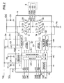
- FIG. 2 shows an example of the detailed diagram of the motor driving semiconductor device 10 having the dead time generation function.
- T1 to T6 indicate six switching elements for driving a three-phase motor.
- IGBT as a power semiconductor switching element
- a power MOSFET and a bipolar transistor may also be used.
- D1 to D6 indicate flywheel diodes connected in reverse parallel with IGBT's.
- P9 indicates a U-phase output terminal
- P10 indicates a V-phase output terminal
- P11 indicates a W-phase output terminal.
- VUT which is a U-phase upper arm control signal is input from a U-phase upper arm control signal input terminal P1 and transmitted to a logical circuit LG1, to a dead time generator circuit DL1, to an upper arm drive circuit KT and to a U-phase upper arm IGBT T1.
- VVT which is a V-phase upper arm control signal is input from a V-phase upper arm control signal input terminal P2 and transmitted to the logical circuit LG1, to the dead time generator circuit DL1, to the upper arm drive circuit KT and to a V-phase upper arm IGBT T2.
- VWT which is a W-phase upper arm control signal is input from a W-phase upper arm control signal input terminal P3 and transmitted to the logical circuit LG1, to the dead time generator circuit DL1, to the upper arm drive circuit KT and to a W-phase upper arm IGBT T3.
- VUB which is a U-phase lower arm control' signal is input from a U-phase lower arm control signal input terminal P4 and transmitted to the logical circuit LG1, to the dead time generator circuit DL1, to a lower arm drive circuit KB and to a U-phase lower arm IGBT T4.
- VVB which is a V-phase lower arm control signal is input from a V-phase lower arm control signal input terminal P5 and transmitted to the logical circuit LG1, to the dead time generator circuit DL1, to the lower arm drive circuit KB and to a V-phase lower arm IGBT T5.
- VWB which is a W-phase lower arm control signal is input from a W-phase lower arm control signal input terminal P6 and transmitted to the logical circuit LG1, to the dead time generator circuit DL1, to the lower arm drive circuit KB and to a W-phase lower arm IGBT T6.
- a charge pump circuit CH is a circuit for generating a power supply voltage VCP for driving the upper arm IGBT's.
- the charge pump circuit has external components including diodes D7 and D8 and capacitors C3 and C4.
- the diodes D7 and D8 may be built in the motor driving semiconductor device 10 having the dead time generation function.
- a clock signal VCL for operating the charge pump circuit CH is input to the charge pump circuit CH via a clock signal input terminal P12. Although not shown in Fig. 1, the clock signal VCL is output from, for example, the controlling semiconductor device 7.
- An internal power source circuit 11 generates a power supply voltage VB of the controlling semiconductor device 7 from the drive circuit power supply voltage Vcc.
- VB is used as the power supply voltage of the controlling semiconductor device 7 and also as the power supply voltage of some circuits in the motor driving semiconductor device 10 having the dead time generation function.
- a current polarity detector circuit 13 detects, for example, a U-phase current polarity and outputs a U-phase current polarity signal VUP from a current polarity signal output terminal P7.
- the current polarity signal may be a V-phase or W-phase current polarity signal instead of the U-phase polarity signal.
- a Vcc-low-voltage detection circuit 14A monitors the drive circuit power supply voltage Vcc, and when the drive circuit power supply voltage Vcc becomes a threshold voltage or lower, outputs a low voltage detection signal to a fault circuit 14C.
- the fault circuit 14C outputs an off signal to the logical circuit LG1 and outputs a fault signal Vf from a fault signal output terminal P8, upon reception of the Vcc low voltage detection signal from the insufficient Vcc voltage detector circuit 14C or an overcurrent detection signal from an overcurrent detector circuit 14B.
- the fault circuit 14C Upon reception of the Vcc low voltage detection signal or overcurrent detection signal, the fault circuit 14C outputs an off command signal to the logical circuit LG1.
- the logical circuit LG1 Upon reception of the off command signal from the fault circuit 14C, the logical circuit LG1 outputs a signal to turn off all IGBT's irrespective of whether the control signals VUT, VVT, VWT, VUB, VVB and VWB take H or L.
- the motor driving semiconductor device 10 having the dead time generation function turns off the switching elements upon detection of an abnormal state such as overcurrent and low Vcc voltage.
- the motor driving semiconductor device 10 having the dead time generation function may not turn off the switching elements but may output the fault signal Vf indicating an abnormal event to the controlling semiconductor device 7, and the controlling semiconductor device 7 outputs a control signal to turn off the switching elements.
- C1, C2 and C5 shown in Fig. 2 are power supply voltage stabilizing capacitors.
- the motor driving semiconductor device 10 having the dead time generation function is constituted of one semiconductor chip, high and low voltage breakdown components exist mixedly in the single semiconductor chip. Each component in the semiconductor chip is electrically isolated by dielectric isolation (DI), SOI, PN junction isolation or the like.
- DI dielectric isolation
- SOI SOI
- PN junction isolation PN junction isolation
- the motor driving semiconductor device 10 having the dead time generation function is constituted of one semiconductor device sealed in one package with resin such as epoxy based resin mixed with filler such as silica.
- the motor driving semiconductor device 10 may be constituted of a plurality of resin sealed semiconductor devices.
- the motor driving semiconductor device 10 having the dead time generation function is constituted of one resin sealed semiconductor device to make the motor driving semiconductor device 10 compact.
- the motor driving semiconductor device 10 having the dead time generation function, and the controlling semiconductor device 7 are constituted of two discrete resin sealed semiconductor devices.
- the semiconductor devices 10 and 7 may be constituted of one resin sealed semiconductor device.
- the switching elements of the motor driving semiconductor device 10 having the dead time generation function generate heat and raise their temperatures during motor driving. In order to prevent the high temperature from being transferred to the controlling semiconductor device 7, it is necessary to use different stages on which chips are mounted, even if the motor driving semiconductor device 10 having the dead time generation function, and the controlling semiconductor 7 are constituted of one resin sealed semiconductor device.
- a general package cannot be used and a special package is required to be used, resulting in a rise in cost.
- the motor driving semiconductor device 10 having the dead time generation function, and the controlling semiconductor device 7 be constituted of two discrete resin sealed semiconductor devices.
- the motor driving semiconductor device 10 having the dead time generation function contains all of the dead time generator circuit DL1, upper arm drive circuit KT, lower arm drive circuit KB and switching elements T1 to T6, in one resin sealed semiconductor device.
- Delay times from the dead time generator circuit DL1 to the switching elements T1 to T6 L1 can therefore be known correctly. Therefore, for example, by setting a dead time generated at the dead time generator circuit DL1 longer than the delay times from the dead time generator circuit DL1 to the switching elements T1 to T6, it is possible to perfectly avoid breakages of the motor driving semiconductor device 10 having the dead time generation function, otherwise to be caused by upper and lower through conduction.
- Fig. 3 is the first example of the logical circuit LG1 and dead time generator circuit DL1.
- the logical circuit LG1 and dead time generator circuit DL1 have circuits of three phases including the U-, V- and W-phases, only the circuit for the U-phase are shown in Fig. 3, omitting the V- and W-phases.
- a U-phase logical circuit LG1_U has NOT circuits L1, L2, L4, L9, L10 and L12 and NAND circuits L3 and L11.
- a U-phase dead time generator circuit DL1_U has NOT circuits L6, L7, L8, L14, L15 and L16, NAND circuits L5 and L13, resistors R1 and R2 and capacitors C1 and C2.
- U-phase upper arm control signals VUT, VUT1 and VUT2 each have an on-signal of "H” and an off signal of "L”.
- U-phase lower arm control signals VUB, VUB1 and VUB2 each have an on-signal of "H” and an off signal of "L”.
- the U-phase upper arm control signal VUT is input to the U-phase logical circuit LG1_U and transmitted to the NOT circuit L1, to the NOT circuit L2, to the NAND circuit L3 and to the NOT circuit L4 to be output from the U-phase logical circuit LG1_U as the U-phase upper arm control signal VUT1.
- the U-phase upper arm control signal VUT1 is input to the U-phase dead time generator circuit DL1_U and transmitted to the NAND circuit L5, to the NOT circuit L6, to a CR circuit constituted of the resistor R1 and capacitor C1, to the NOT circuit L7 and to the NOT circuit L8 to be output from the U-phase dead time generator circuit DL1_U as the U-phase upper arm control signal VUT2.
- the U-phase lower arm control signal VUB is input to the U-phase logical circuit LG1_U and transmitted to the NOT circuit L9, to the NOT circuit L10, to the NAND circuit L11 and to the NOT circuit L12 to be output from the U-phase logical circuit LG1_U1 as the U-phase lower arm control signal VUB1.
- the U-phase lower arm control signal VUB1 is input to the U-phase dead time generator circuit DL1_U and transmitted to the NAND circuit L13, to the NOT circuit L14, to a CR circuit constituted of the resistor R2 and capacitor C2, to the NOT circuit L15 and to the NOT circuit L16 to be output from the U-phase dead time generator circuit DL1_U as the U-phase lower arm control signal VUB2.
- the fault circuit 14C outputs normally "H” to the NAND circuits L3 and L11, and when an off command is to be output, outputs "L” to the NAND circuits L3 and L11.
- An output signal of the NOT circuit L1 is input not only to the NOT circuit L2, but also to the NAND circuit L11. The reason for this is to prevent an on-signal from being transmitted to the U-phase lower arm switching element while the U-phase upper arm control signal VUT takes "H".
- an output signal of the NOT circuit L9 is input not only to the NOT circuit L10, but also to the NAND circuit L3. The reason for this is to prevent an on-signal from being transmitted to the U-phase upper arm switching element while the U-phase lower arm control signal VUT takes "H”.
- An output signal of the NOT circuit L7 is input not only to the NOT circuit L8 but also to the NAND circuit L13.
- the reason for this is to prevent the U-phase lower arm on-signal from transmitting to the stage after L13-until an off-signal ("L") is transmitted to the NOT circuit L8 after the U-phase upper arm control signal VUT1 changes from an on-signal ("H") to the off-signal.
- an output signal of the NOT circuit L15 is input not only to the NOT circuit L16 but also to the NAND circuit L5.
- the reason for this is to prevent the U-phase upper arm on-signal from transmitting to the stage after L5 until an off-signal ("L") is transmitted to the NOT circuit L16 after the U-phase lower arm control signal VUB1 changes from an on-signal ("H") to the off-signal (L").
- a dead time is therefore formed between the U-phase upper arm control signal VUT2 and U-phase lower arm control signal VUB2.
- the dead time generated when the U-phase upper arm control signal VUT1 changes from the on- - signal to off-signal and at the same time the U-phase lower arm control signal VUB1 changes from the off-signal to on-signal, is approximately the delay time by the CR circuit constituted of the resistor R1 and capacitor C1.
- the U-phase dead time generator circuit DL1_U outputs the dead time without changing it. Further, the dead time, generated when the U-phase lower arm control signal VUB1 changes from the on-signal to off-signal and at the same time the U-phase upper arm control signal VUT1 changes from the off-signal to on-signal, is approximately the delay time by the CR circuit constituted of the resistor R2 and capacitor C2.
- the U-phase dead time generator circuit DL1_U outputs the dead time without changing it.
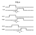
- Figs. 4 to 7 are timing charts illustrating the operations of the U-phase logical circuit LG1_U and U-phase dead time generator circuit DL1-U shown in Fig. 3. These timing charts show the dead time while the U-phase upper arm control signal changes from the on-signal to off-signal and the U-phase lower arm control signal changes from the off-signal to on-signal.
- Ta shown in Figs. 4 and 6 indicates the dead time generated by the CR circuit constituted of the resistor R1 and capacitor C1 in the U-phase dead time generator circuit DL1_U.
- Fig. 4 shows the case in which there is a dead time having a time duration of T1 shorter than Ta between the U-phase upper arm control signal VUT and U-phase lower arm control signal VUB.
- a dead time is T1 between the U-phase upper arm control signal VUT1 and U-phase lower arm control signal VUB1. Since T1 ⁇ Ta, the U-phase dead time generator circuit DL1_U prolongs the dead time to set the dead time Ta between the U-phase upper arm control signal VUT2 and U-phase lower arm control signal VUB2.
- Fig. 5 shows the case in which there is a dead time having a time duration of T2 longer than Ta between the U-phase upper arm control signal VUT and U-phase lower arm control signal VUB.
- a dead time is T2 between the U-phase upper arm control signal VUT1 and U-phase lower arm control signal VUB1. Since T2 > Ta, the U-phase dead time generator circuit DL1_U does not prolong the dead time to set the dead time T2 between the U-phase upper arm control signal VUT2 and U-phase lower arm control signal VUB2.
- Fig. 6 shows the case in which both the U-phase upper arm control signal VUT and U-phase lower arm control signal VUB take “H” during a period of T3 shorter than Ta. Both signals during the period of "H” are output as signals "L” by the U-phase logical circuit LG1_U. Therefore, a dead time having a time duration of T3 is generated between the U-phase upper arm control signal VUT1 and U-phase lower arm control signal VUB1. Since T3 ⁇ Ta, the U-phase dead time generator circuit DL1_U prolongs the dead time to set the dead time Ta between the U-phase upper arm control signal VUT2 and U-phase lower arm control signal VUB2.
- Fig. 7 shows the case in which both the U-phase upper arm control signal VUT and U-phase lower arm control signal VUB take “H” during a period of T4 longer than Ta. Both signals during the period of "H” are output as signals "L” by the U-phase logical circuit LG1_U. Therefore, a dead time having a time duration of T4 is generated between the U-phase upper arm control signal VUT1 and U-phase lower arm control signal VUB1. Since T4 > Ta, the U-phase dead time generator circuit DL1_U does not prolong the dead time to set the dead time T4 between the U-phase upper arm control signal VUT2 and U-phase lower arm control signal VUB2.
- Fig. 8 is a diagram showing an example of the relation between a dead time between the U-phase upper arm control signal VUT and U-phase lower arm control signal VUB and a dead time between the U-phase upper arm control signal VUT2 and U-phase lower arm control signal VUB2.
- the abscissa represents a dead time between the U-phase upper arm control signal VUT and U-phase lower arm control signal VUB
- the ordinate represents a dead time between the U-phase upper arm control signal VUT2 and U-phase lower arm control signal VUB2.
- a minus sign of the dead time of the abscissa between the U-phase upper arm control signal VUT and U-phase lower arm control signal VUB means the period while both the U-phase upper arm control signal VUT and U-phase lower arm control signal VUB take "H". For example, if both the U-phase upper arm control signal VUT and U-phase lower arm control signal VUB take "H" during a period of 3 ⁇ s, a dead time (abscissa) between the U-phase upper arm control signal VUT and U-phase lower arm control signal VUB is - 3 ⁇ s in Fig. 8.
- Ta 2 ⁇ s.
- Ta takes generally a value of about 1 ⁇ s to 10 ⁇ s.
- a dead time equal to or longer than Ta is essentially generated between the U-phase upper arm control signal.VUT2 and U-phase lower arm control signal VUB2 respectively output from the U-phase dead time generator circuit DL1-U. If there is a dead time equal to or longer than Ta between the U-phase upper arm control signal VUT and U-phase lower arm control signal VUB, the dead time is not prolonged and is output without being changed.
- the dead time generation function of the motor driving semiconductor device 10 has the performance described above. Therefore, a dead time can be retained by all means in the motor driving semiconductor device 10 having the dead time generation function, even if an abnormal state occurs in the controlling semiconductor device or noises are superposed upon the control signal input to the motor driving semiconductor device 10 having the dead time generation function. Accordingly, the motor driving semiconductor device 10 having the dead time generation function, will not be broken otherwise to be caused by upper and lower electrical shortage.
- the controlling semiconductor device 7 In performing the sine wave driving method by using the controlling semiconductor device such as a microcomputer, the controlling semiconductor device 7 has often the dead time generation function, and the dead time generated by the controlling semiconductor device is often compensated in the controlling semiconductor device.
- the dead time generation function of the present invention if the dead time of input control signals is equal to or longer than a predetermined value, the dead time is not changed and this value is set shorter than the dead time to be generated by the controlling semiconductor device 7. Since the motor driving semiconductor device 10 having the dead time generation function, does not change the dead time generated by the controlling semiconductor device 7 in a normal case, the dead time can be compensated correctly.
- the motor driving semiconductor device 10 having the dead time generation function retains the dead time, it is possible to prevent breakage of the motor driving semiconductor device 10 having the dead time generation function, even if an abnormal state occurs in the controlling semiconductor device 7 or noises are superposed upon the control signal input to the motor driving semiconductor device 10 having the dead time generation function.
- Fig. 9 shows the second embodiment. This embodiment pertains to a second example of the logical circuit LG1 and dead time generator circuit DL1.
- the circuit shown in Fig. 9 deletes the NAND circuits L3, L5, L11 and L13 and the NOT circuits L4 and L12 from the circuit Fig. 3D, and adds NAND circuits L17 and L18.
- the NAND circuit L17 shown in Fig. 9 realizes the operations of the NAND circuits L3 and L5 shown in Fig. 3, and the NAND circuit 18 shown in Fig. 9 realizes the operations of the NAND circuits L11 and L13 shown in Fig. 3.
- the operation of the circuit shown in Fig. 9 is similar to that of the circuit shown in Fig. 3, and the detailed description thereof is omitted.
- Fig. 10 shows the third embodiment.
- NMOSFET's are used as switching elements T1' to T6' shown in Fig. 10
- IGBT's or bipolar transistors may also be used.
- PMOSFET's may be used as the upper arm switching elements T1' to T3'.
- parasitic diodes in MOSFET's may be used instead of flywheel diodes.
- the motor driving semiconductor device 10 having the dead time generation function is divided into a pre-drive semiconductor device 10A having the dead time generation function and a motor drive switching device 10B.
- the other structures are similar to those shown in Fig. 2, and the detailed description thereof is omitted.
- the pre-drive portion is constituted of one pre-drive semiconductor device 10A having the dead time generation function and sealed in one package with resin such as epoxy based resin mixed with filler such as silica
- the pre-drive portion may be constituted of a plurality of IC's.
- the pre-drive portion may be constituted of three pre-drive semiconductor devices having the dead time generation function for respective phases. If PMOSFET's or PNP transistors are used as the upper arm switching elements, the pre-drive portion can be realized by a very simple circuit structure. Therefore, the pre-drive portion may be constituted of a discrete circuit using bipolar transistors, resistors and the like without using IC's.
- the motor drive switching device 10B is sealed in one package with resin
- the device may be realized by using a plurality of packages.
- the upper arm switching elements and the lower arm switching elements may be sealed in different packages with resin
- six switching elements may be sealed in six different packages
- the upper arm switching element and lower arm switching element for each phase may be sealed in one package to use three packages in total.
- the motor drive switching device 10B is a discrete component, a motor drive power can be adjusted properly by selecting a suitable motor drive switching device 10B.
- the pre-drive semiconductor device 10A Since the pre-drive semiconductor device 10A has the dead time generation function, it is possible to prevent breakage of the motor drive switching device 10B otherwise to be caused by upper and lower through conduction.
- Fig. 11 shows an example of the structure of the motor 5 adopted in this embodiment.
- a motor shown in Fig. 11 is a three-phase motor.
- Disposed on a board 6 built in the motor are the controlling semiconductor device 7, semiconductor device 10 for driving the motor, having the dead time generation function, high power supply voltage detector circuit 15, temperature detector circuit 16, shunt resistor Rs and Hall IC 9, respectively of the first embodiment shown in Fig. 1.
- coils 8 are fitted in a motor housing lower portion 5B, and a permanent magnet rotor 22 is disposed inside the coils 8, being set not to contact the coils by involving a proper gap therebetween.
- the board 6 built in the motor is disposed above the permanent magnet rotor 22.
- the Hall IC 9 is mounted on the board 6 on the side of the permanent magnet rotor 22 (on the bottom side in Fig. 11).
- the controlling semiconductor device 7, high power supply voltage detector circuit 15, temperature detector circuit 16 and shunt resistor Rs are mounted on the board on the side of the permanent magnet rotor 22 (on the bottom side in Fig. 11), and the motor driving semiconductor device 10 having the dead time generation function, is mounted on the board on the side opposite to the permanent magnet rotor 22 (on the top side in Fig. 11).
- the thermistor in the temperature detector circuit 16 is disposed near the controlling semiconductor device 7, whereas if the temperature detector circuit 16 is to be used for detecting a temperature of the motor driving semiconductor device 10 having the dead time generation function, the thermistor in the temperature detector circuit 16 is disposed near the motor driving semiconductor device 10 having the dead time generation function.
- Coil connection terminals 21 are disposed on the board 6, and the coils 8 are connected to the terminals by soldering.
- Lead wirings 20 are connected to the board 6 by soldering.
- the lead wirings 20 include five wirings: a VDC wiring, a Vcc wiring, a Vsp wiring, an FG wiring, and a GND wiring.
- a motor housing upper portion 5A is mounted above the board 6 like a cap. In an assembled state of the motor, the board 6 is disposed inside the motor housing constituted of the motor housing upper portion 5A and motor housing lower portion 5B.
- the motor 5 may have molded coils 8 without using the housing lower portion 5B of the motor 5.
- the motor may have molded coils 8 and the board 6 without using the housing upper portion 5A and housing lower portion 5B of the motor 5.
- the motor of the fourth embodiment is applied to an air conditioner.
- an outdoor apparatus is equipped with a compressor for compressing refrigerant, an outdoor heat exchanger, a compressor drive motor for driving the compressor and an outdoor fan motor for blowing air to the outdoor heat exchanger
- an indoor apparatus is equipped with an indoor heat exchanger and an indoor fan motor for blowing air to the indoor heat exchanger.
- anti-vibration rubber is used for the 120-degree rectangular wave driving type motor.
- the anti-vibration rubber is used, for example, at a fixing part for fixing the fan motor to the main body of the outdoor apparatus and at a position between a permanent magnet and a shaft of the permanent or between the shaft and fan.
- torque ripples of the motor are reduced by the sine wave driving method to reduce vibrations of the motor. It is therefore possible to reduce noises even if anti-vibration rubber is not used. In order to further reduce noises, obviously it is possible to use anti-vibration rubber for the motor of the present invention.
- the outdoor apparatus of the air conditioner has many noises from the compressor drive motor. Therefore, if the controlling semiconductor device 7 is disposed in the inside of the outdoor apparatus of the air conditioner, the controlling semiconductor device 7 is likely to enter an abnormal state because of noises, and noises are likely to superpose upon control signals.
- the outdoor apparatus of the air conditioner is provided with the advantages of reliably ensuring the dead time to prevent breakage of the motor driving semiconductor device 10 otherwise to be caused by upper and lower trough conduction thereof, if an abnormal state occurs in the controlling semiconductor device 7 or noises are applied to control signals.
- the motor of the fourth embodiment may be used as the indoor apparatus fan motor of the air conditioner. Also in this case, since the motor has small vibrations, the indoor apparatus can be run with small noises similar to the outdoor apparatus, and breakage to be caused by upper and lower through conduction can be prevented so that high reliability is ensured.
Landscapes
- Engineering & Computer Science (AREA)
- Power Engineering (AREA)
- Inverter Devices (AREA)
- Control Of Motors That Do Not Use Commutators (AREA)
Applications Claiming Priority (1)
| Application Number | Priority Date | Filing Date | Title |
|---|---|---|---|
| JP2006146082A JP4742989B2 (ja) | 2006-05-26 | 2006-05-26 | モータ駆動用半導体装置とそれを有するモータ及びモータ駆動装置並びに空調機 |
Publications (3)
| Publication Number | Publication Date |
|---|---|
| EP1860767A2 true EP1860767A2 (de) | 2007-11-28 |
| EP1860767A3 EP1860767A3 (de) | 2009-12-30 |
| EP1860767B1 EP1860767B1 (de) | 2012-08-01 |
Family
ID=38476838
Family Applications (1)
| Application Number | Title | Priority Date | Filing Date |
|---|---|---|---|
| EP07010278A Active EP1860767B1 (de) | 2006-05-26 | 2007-05-23 | Halbleitervorrichtung für eine Motoransteuerung und dieselbige enthaltender Motor, Motoransteuerungsvorrichtung und Luftkühlanlage |
Country Status (3)
| Country | Link |
|---|---|
| US (1) | US7710064B2 (de) |
| EP (1) | EP1860767B1 (de) |
| JP (1) | JP4742989B2 (de) |
Cited By (2)
| Publication number | Priority date | Publication date | Assignee | Title |
|---|---|---|---|---|
| EP1971020A2 (de) | 2007-03-16 | 2008-09-17 | Hitachi, Ltd. | Halbleiterbaugruppe für einen Antriebsmotor, Dreiphasenmotor sowie Motorantriebsvorrichtung mit der Halbleiterbaugruppe und Lüftermotor |
| CN105703690A (zh) * | 2014-12-13 | 2016-06-22 | 包米勒公司 | 变频器 |
Families Citing this family (14)
| Publication number | Priority date | Publication date | Assignee | Title |
|---|---|---|---|---|
| JP2009081930A (ja) * | 2007-09-26 | 2009-04-16 | Jtekt Corp | モータ制御装置および電動パワーステアリング装置 |
| JP5097228B2 (ja) * | 2010-02-24 | 2012-12-12 | パナソニック株式会社 | モータ及びそれを備えたポンプ |
| JP5453183B2 (ja) * | 2010-06-25 | 2014-03-26 | パナソニック株式会社 | モータ及びそれを備えたポンプ |
| US9083244B2 (en) * | 2010-12-02 | 2015-07-14 | Mitsubishi Electric Corporation | Power conversion apparatus |
| KR101272595B1 (ko) * | 2011-12-12 | 2013-06-11 | 기아자동차주식회사 | Dc 모터용 스위칭 소자 제어 장치 및 방법 |
| JP2013158219A (ja) * | 2012-01-31 | 2013-08-15 | Nippon Densan Corp | モータユニット |
| US9347837B2 (en) | 2012-04-17 | 2016-05-24 | Honeywell International Inc. | Multi-phase brushless DC motor control integrated circuit having magnetic sensor and band-gap temperature sensor formed thereon |
| JP2014007856A (ja) * | 2012-06-25 | 2014-01-16 | Mitsubishi Electric Corp | 送風機 |
| US9160269B2 (en) * | 2013-03-01 | 2015-10-13 | Regal Beloit America, Inc. | Motor assembly with integrated on/off detection with speed profile operation |
| JP6650626B2 (ja) * | 2015-03-13 | 2020-02-19 | パナソニックIpマネジメント株式会社 | 非接触給電装置および非接触給電システム |
| WO2018020615A1 (ja) * | 2016-07-27 | 2018-02-01 | 三菱電機株式会社 | 電力変換装置 |
| JP2019161891A (ja) | 2018-03-14 | 2019-09-19 | 日本電産株式会社 | モータの制御装置およびモータの制御方法 |
| TWI711239B (zh) * | 2019-12-27 | 2020-11-21 | 新唐科技股份有限公司 | 晶片以及其升溫電路與升溫控制方法 |
| CN119908066A (zh) * | 2022-12-21 | 2025-04-29 | 日立安斯泰莫株式会社 | 电动机控制装置以及电动机控制方法 |
Family Cites Families (31)
| Publication number | Priority date | Publication date | Assignee | Title |
|---|---|---|---|---|
| JP3242729B2 (ja) | 1993-02-18 | 2001-12-25 | 東芝キヤリア株式会社 | 空気調和装置の制御装置 |
| JPH0731162A (ja) | 1993-07-08 | 1995-01-31 | Toshiba Corp | インバータ回路の制御方法 |
| US5506484A (en) * | 1994-06-10 | 1996-04-09 | Westinghouse Electric Corp. | Digital pulse width modulator with integrated test and control |
| JPH07337080A (ja) * | 1994-06-10 | 1995-12-22 | Hitachi Ltd | 空気調和機 |
| JP3356551B2 (ja) | 1994-07-13 | 2002-12-16 | 東芝キヤリア株式会社 | 空気調和機 |
| US6032869A (en) * | 1996-04-03 | 2000-03-07 | Denso Corporation | Heating apparatus for vehicle |
| JPH09331682A (ja) * | 1996-06-12 | 1997-12-22 | Meidensha Corp | 電力変換器 |
| US5671130A (en) * | 1996-08-23 | 1997-09-23 | Allen-Bradley Company, Inc. | Method and apparatus for controlling voltage reflections using a motor controller |
| JP3372436B2 (ja) * | 1996-11-28 | 2003-02-04 | オークマ株式会社 | インバータの制御装置 |
| US6492719B2 (en) * | 1999-07-30 | 2002-12-10 | Hitachi, Ltd. | Semiconductor device |
| JP3708292B2 (ja) * | 1997-06-17 | 2005-10-19 | 三菱電機株式会社 | Pwmインバータ装置の制御方法および制御装置 |
| US5917721A (en) * | 1997-11-21 | 1999-06-29 | Allen-Bradley Company, Llc | Apparatus for reducing the effects of turn on delay errors in motor control |
| JP2000092886A (ja) * | 1998-09-14 | 2000-03-31 | Mitsubishi Electric Corp | 電動機駆動装置 |
| US6324085B2 (en) * | 1999-12-27 | 2001-11-27 | Denso Corporation | Power converter apparatus and related method |
| JP2001128417A (ja) | 2000-09-18 | 2001-05-11 | Hitachi Ltd | 電動機 |
| JP3641232B2 (ja) | 2001-11-13 | 2005-04-20 | 本田技研工業株式会社 | インバータ装置及びその製造方法 |
| US6714424B2 (en) * | 2001-11-30 | 2004-03-30 | Ballard Power Systems Corporation | Dead-time compensation with narrow pulse elimination in solid- state switch devices |
| JP3854190B2 (ja) * | 2002-04-26 | 2006-12-06 | 株式会社ジェイテクト | モータ制御装置 |
| JP3831296B2 (ja) * | 2002-05-24 | 2006-10-11 | 株式会社東芝 | 三相モータ駆動装置 |
| US6958922B2 (en) * | 2002-07-22 | 2005-10-25 | Magnetic Design Labs Inc. | High output power quasi-square wave inverter circuit |
| JP3888272B2 (ja) | 2002-09-25 | 2007-02-28 | 株式会社日立製作所 | 交流電動機の制御装置及び半導体装置 |
| US7045884B2 (en) * | 2002-10-04 | 2006-05-16 | International Rectifier Corporation | Semiconductor device package |
| JP2004215406A (ja) * | 2002-12-28 | 2004-07-29 | Daikin Ind Ltd | 空気調和装置用モータ駆動装置 |
| JP3879688B2 (ja) | 2003-03-26 | 2007-02-14 | 株式会社デンソー | 半導体装置 |
| US20040232864A1 (en) * | 2003-05-23 | 2004-11-25 | Hideki Sunaga | Apparatus for controlling motor |
| JP4239723B2 (ja) * | 2003-07-24 | 2009-03-18 | トヨタ自動車株式会社 | 発電電動装置を備える駆動システムおよび発電電動装置の制御をコンピュータに実行させるためのプログラムを記録したコンピュータ読取り可能な記録媒体 |
| JP4157010B2 (ja) * | 2003-10-27 | 2008-09-24 | 三菱電機株式会社 | 駆動回路及び半導体装置 |
| US20050155369A1 (en) | 2004-01-15 | 2005-07-21 | Toshiba Carrier Corporation | Air conditioner |
| JP4422567B2 (ja) * | 2004-06-30 | 2010-02-24 | 株式会社日立製作所 | モータ駆動装置,電動アクチュエータおよび電動パワーステアリング装置 |
| US7075267B1 (en) * | 2004-12-29 | 2006-07-11 | Prolific Technology Inc. | Space vector-based current controlled PWM inverter for motor drives |
| JP4894312B2 (ja) * | 2005-03-30 | 2012-03-14 | パナソニック株式会社 | インバータ装置 |
-
2006
- 2006-05-26 JP JP2006146082A patent/JP4742989B2/ja active Active
-
2007
- 2007-05-22 US US11/751,747 patent/US7710064B2/en active Active
- 2007-05-23 EP EP07010278A patent/EP1860767B1/de active Active
Cited By (6)
| Publication number | Priority date | Publication date | Assignee | Title |
|---|---|---|---|---|
| EP1971020A2 (de) | 2007-03-16 | 2008-09-17 | Hitachi, Ltd. | Halbleiterbaugruppe für einen Antriebsmotor, Dreiphasenmotor sowie Motorantriebsvorrichtung mit der Halbleiterbaugruppe und Lüftermotor |
| EP1971020A3 (de) * | 2007-03-16 | 2011-09-21 | Hitachi, Ltd. | Halbleiterbaugruppe für einen Antriebsmotor, Dreiphasenmotor sowie Motorantriebsvorrichtung mit der Halbleiterbaugruppe und Lüftermotor |
| CN105703690A (zh) * | 2014-12-13 | 2016-06-22 | 包米勒公司 | 变频器 |
| EP3032732A3 (de) * | 2014-12-13 | 2016-07-27 | Baumüller Nürnberg GmbH | Umrichter |
| US9762172B2 (en) | 2014-12-13 | 2017-09-12 | Baumueller Nuernberg Gmbh | Converter |
| AT17880U1 (de) * | 2014-12-13 | 2023-06-15 | Baumueller Nuernberg Gmbh | Umrichter |
Also Published As
| Publication number | Publication date |
|---|---|
| EP1860767A3 (de) | 2009-12-30 |
| JP2007318921A (ja) | 2007-12-06 |
| US7710064B2 (en) | 2010-05-04 |
| EP1860767B1 (de) | 2012-08-01 |
| US20070273312A1 (en) | 2007-11-29 |
| JP4742989B2 (ja) | 2011-08-10 |
Similar Documents
| Publication | Publication Date | Title |
|---|---|---|
| EP1860767B1 (de) | Halbleitervorrichtung für eine Motoransteuerung und dieselbige enthaltender Motor, Motoransteuerungsvorrichtung und Luftkühlanlage | |
| JP4586034B2 (ja) | モータ駆動用半導体装置とそれを有する3相モータ及びモータ駆動装置並びにファンモータ | |
| JP6270549B2 (ja) | 半導体装置およびそれを用いるモータ並びに空調機 | |
| JP3419157B2 (ja) | モータ駆動方法及びそれを用いた電気機器 | |
| JP6091632B2 (ja) | 電力変換装置 | |
| JP5556353B2 (ja) | モータ電流検出器及びモータ制御装置 | |
| US20120256573A1 (en) | Motor driving device, and control method of motor driving device | |
| EP2224587B1 (de) | Schaltkreis zur Erfassung induzierter Spannung, Motorantriebshalbleiterbauelement mit diesem Schaltkreis, Motor und Klimaanlage | |
| KR101085962B1 (ko) | 반도체장치와 그것을 가지는 모터 및 모터 구동장치 | |
| JP4682985B2 (ja) | ブラシレスdcモータおよびそれを搭載した電気機器 | |
| JP4899801B2 (ja) | 半導体装置とそれを有するモータ及びモータ駆動装置 | |
| CN100376076C (zh) | Mos型fet、及配有它的电机驱动装置和电机 | |
| EP3960381B1 (de) | Elektrische vorrichtung | |
| JP4749663B2 (ja) | モータの制御装置 | |
| JP3831296B2 (ja) | 三相モータ駆動装置 | |
| US12438420B2 (en) | Electric motor, air conditioner, and control board | |
| KR101335619B1 (ko) | 스위치드 릴럭턴스 모터 구동용 고집적 반도체 모듈 | |
| WO2023135743A1 (ja) | 電動機、空気調和機、および制御基板 | |
| WO2024047863A1 (ja) | 電動機、空気調和機、および制御基板 | |
| KR20080097283A (ko) | 모터 구동 장치 | |
| JP2000092886A (ja) | 電動機駆動装置 |
Legal Events
| Date | Code | Title | Description |
|---|---|---|---|
| PUAI | Public reference made under article 153(3) epc to a published international application that has entered the european phase |
Free format text: ORIGINAL CODE: 0009012 |
|
| AK | Designated contracting states |
Kind code of ref document: A2 Designated state(s): AT BE BG CH CY CZ DE DK EE ES FI FR GB GR HU IE IS IT LI LT LU LV MC MT NL PL PT RO SE SI SK TR |
|
| AX | Request for extension of the european patent |
Extension state: AL BA HR MK YU |
|
| 17P | Request for examination filed |
Effective date: 20090406 |
|
| PUAL | Search report despatched |
Free format text: ORIGINAL CODE: 0009013 |
|
| AK | Designated contracting states |
Kind code of ref document: A3 Designated state(s): AT BE BG CH CY CZ DE DK EE ES FI FR GB GR HU IE IS IT LI LT LU LV MC MT NL PL PT RO SE SI SK TR |
|
| AX | Request for extension of the european patent |
Extension state: AL BA HR MK RS |
|
| RIC1 | Information provided on ipc code assigned before grant |
Ipc: H02P 25/02 20060101AFI20070919BHEP Ipc: H02M 1/38 20070101ALI20091120BHEP |
|
| 17Q | First examination report despatched |
Effective date: 20100326 |
|
| AKX | Designation fees paid |
Designated state(s): DE FR |
|
| GRAP | Despatch of communication of intention to grant a patent |
Free format text: ORIGINAL CODE: EPIDOSNIGR1 |
|
| GRAS | Grant fee paid |
Free format text: ORIGINAL CODE: EPIDOSNIGR3 |
|
| GRAA | (expected) grant |
Free format text: ORIGINAL CODE: 0009210 |
|
| AK | Designated contracting states |
Kind code of ref document: B1 Designated state(s): DE FR |
|
| REG | Reference to a national code |
Ref country code: DE Ref legal event code: R096 Ref document number: 602007024259 Country of ref document: DE Effective date: 20120927 |
|
| PLBE | No opposition filed within time limit |
Free format text: ORIGINAL CODE: 0009261 |
|
| STAA | Information on the status of an ep patent application or granted ep patent |
Free format text: STATUS: NO OPPOSITION FILED WITHIN TIME LIMIT |
|
| 26N | No opposition filed |
Effective date: 20130503 |
|
| REG | Reference to a national code |
Ref country code: DE Ref legal event code: R097 Ref document number: 602007024259 Country of ref document: DE Effective date: 20130503 |
|
| REG | Reference to a national code |
Ref country code: DE Ref legal event code: R082 Ref document number: 602007024259 Country of ref document: DE Representative=s name: MERH-IP MATIAS ERNY REICHL HOFFMANN, DE |
|
| REG | Reference to a national code |
Ref country code: DE Ref legal event code: R081 Ref document number: 602007024259 Country of ref document: DE Owner name: HITACHI POWER SEMICONDUCTOR DEVICE, LTD., HITA, JP Free format text: FORMER OWNER: HITACHI, LTD., TOKYO, JP Effective date: 20120803 Ref country code: DE Ref legal event code: R082 Ref document number: 602007024259 Country of ref document: DE Representative=s name: MERH-IP MATIAS ERNY REICHL HOFFMANN, DE Effective date: 20141127 Ref country code: DE Ref legal event code: R081 Ref document number: 602007024259 Country of ref document: DE Owner name: HITACHI POWER SEMICONDUCTOR DEVICE, LTD., HITA, JP Free format text: FORMER OWNER: HITACHI, LTD., TOKYO, JP Effective date: 20141127 Ref country code: DE Ref legal event code: R082 Ref document number: 602007024259 Country of ref document: DE Representative=s name: MERH-IP MATIAS ERNY REICHL HOFFMANN PATENTANWA, DE Effective date: 20141127 |
|
| REG | Reference to a national code |
Ref country code: FR Ref legal event code: TP Owner name: HITACHI POWER SEMICONDUCTOR DEVICE, LTD., JP Effective date: 20141209 |
|
| REG | Reference to a national code |
Ref country code: FR Ref legal event code: PLFP Year of fee payment: 10 |
|
| REG | Reference to a national code |
Ref country code: FR Ref legal event code: PLFP Year of fee payment: 11 |
|
| REG | Reference to a national code |
Ref country code: FR Ref legal event code: PLFP Year of fee payment: 12 |
|
| REG | Reference to a national code |
Ref country code: FR Ref legal event code: PLFP Year of fee payment: 17 |
|
| REG | Reference to a national code |
Ref country code: DE Ref legal event code: R082 Ref document number: 602007024259 Country of ref document: DE Representative=s name: DENNEMEYER & ASSOCIATES RECHTSANWALTSGESELLSCH, DE Ref country code: DE Ref legal event code: R081 Ref document number: 602007024259 Country of ref document: DE Owner name: MINEBEA POWER SEMICONDUCTOR DEVICE INC., HITAC, JP Free format text: FORMER OWNER: HITACHI POWER SEMICONDUCTOR DEVICE, LTD., HITACHI-SHI, LBARAKI, JP |
|
| PGFP | Annual fee paid to national office [announced via postgrant information from national office to epo] |
Ref country code: DE Payment date: 20250521 Year of fee payment: 19 |
|
| PGFP | Annual fee paid to national office [announced via postgrant information from national office to epo] |
Ref country code: FR Payment date: 20250528 Year of fee payment: 19 |