EP1840979A2 - Halbleiterschicht, Verfahren zu deren Herstellung und lichtemittierendes Halbleiterbauelement - Google Patents
Halbleiterschicht, Verfahren zu deren Herstellung und lichtemittierendes Halbleiterbauelement Download PDFInfo
- Publication number
- EP1840979A2 EP1840979A2 EP07006263A EP07006263A EP1840979A2 EP 1840979 A2 EP1840979 A2 EP 1840979A2 EP 07006263 A EP07006263 A EP 07006263A EP 07006263 A EP07006263 A EP 07006263A EP 1840979 A2 EP1840979 A2 EP 1840979A2
- Authority
- EP
- European Patent Office
- Prior art keywords
- semiconductor
- light emitting
- base plate
- layer
- electrical conduction
- Prior art date
- Legal status (The legal status is an assumption and is not a legal conclusion. Google has not performed a legal analysis and makes no representation as to the accuracy of the status listed.)
- Granted
Links
Images



Classifications
-
- H—ELECTRICITY
- H10—SEMICONDUCTOR DEVICES; ELECTRIC SOLID-STATE DEVICES NOT OTHERWISE PROVIDED FOR
- H10H—INORGANIC LIGHT-EMITTING SEMICONDUCTOR DEVICES HAVING POTENTIAL BARRIERS
- H10H29/00—Integrated devices, or assemblies of multiple devices, comprising at least one light-emitting semiconductor element covered by group H10H20/00
- H10H29/10—Integrated devices comprising at least one light-emitting semiconductor component covered by group H10H20/00
- H10H29/14—Integrated devices comprising at least one light-emitting semiconductor component covered by group H10H20/00 comprising multiple light-emitting semiconductor components
-
- C—CHEMISTRY; METALLURGY
- C30—CRYSTAL GROWTH
- C30B—SINGLE-CRYSTAL GROWTH; UNIDIRECTIONAL SOLIDIFICATION OF EUTECTIC MATERIAL OR UNIDIRECTIONAL DEMIXING OF EUTECTOID MATERIAL; REFINING BY ZONE-MELTING OF MATERIAL; PRODUCTION OF A HOMOGENEOUS POLYCRYSTALLINE MATERIAL WITH DEFINED STRUCTURE; SINGLE CRYSTALS OR HOMOGENEOUS POLYCRYSTALLINE MATERIAL WITH DEFINED STRUCTURE; AFTER-TREATMENT OF SINGLE CRYSTALS OR A HOMOGENEOUS POLYCRYSTALLINE MATERIAL WITH DEFINED STRUCTURE; APPARATUS THEREFOR
- C30B25/00—Single-crystal growth by chemical reaction of reactive gases, e.g. chemical vapour-deposition growth
- C30B25/02—Epitaxial-layer growth
- C30B25/10—Heating of the reaction chamber or the substrate
- C30B25/105—Heating of the reaction chamber or the substrate by irradiation or electric discharge
-
- C—CHEMISTRY; METALLURGY
- C30—CRYSTAL GROWTH
- C30B—SINGLE-CRYSTAL GROWTH; UNIDIRECTIONAL SOLIDIFICATION OF EUTECTIC MATERIAL OR UNIDIRECTIONAL DEMIXING OF EUTECTOID MATERIAL; REFINING BY ZONE-MELTING OF MATERIAL; PRODUCTION OF A HOMOGENEOUS POLYCRYSTALLINE MATERIAL WITH DEFINED STRUCTURE; SINGLE CRYSTALS OR HOMOGENEOUS POLYCRYSTALLINE MATERIAL WITH DEFINED STRUCTURE; AFTER-TREATMENT OF SINGLE CRYSTALS OR A HOMOGENEOUS POLYCRYSTALLINE MATERIAL WITH DEFINED STRUCTURE; APPARATUS THEREFOR
- C30B29/00—Single crystals or homogeneous polycrystalline material with defined structure characterised by the material or by their shape
- C30B29/10—Inorganic compounds or compositions
- C30B29/40—AIIIBV compounds wherein A is B, Al, Ga, In or Tl and B is N, P, As, Sb or Bi
- C30B29/403—AIII-nitrides
-
- H—ELECTRICITY
- H10—SEMICONDUCTOR DEVICES; ELECTRIC SOLID-STATE DEVICES NOT OTHERWISE PROVIDED FOR
- H10H—INORGANIC LIGHT-EMITTING SEMICONDUCTOR DEVICES HAVING POTENTIAL BARRIERS
- H10H20/00—Individual inorganic light-emitting semiconductor devices having potential barriers, e.g. light-emitting diodes [LED]
- H10H20/01—Manufacture or treatment
- H10H20/011—Manufacture or treatment of bodies, e.g. forming semiconductor layers
- H10H20/013—Manufacture or treatment of bodies, e.g. forming semiconductor layers having light-emitting regions comprising only Group III-V materials
- H10H20/0133—Manufacture or treatment of bodies, e.g. forming semiconductor layers having light-emitting regions comprising only Group III-V materials with a substrate not being Group III-V materials
- H10H20/01335—Manufacture or treatment of bodies, e.g. forming semiconductor layers having light-emitting regions comprising only Group III-V materials with a substrate not being Group III-V materials the light-emitting regions comprising nitride materials
-
- H—ELECTRICITY
- H10—SEMICONDUCTOR DEVICES; ELECTRIC SOLID-STATE DEVICES NOT OTHERWISE PROVIDED FOR
- H10P—GENERIC PROCESSES OR APPARATUS FOR THE MANUFACTURE OR TREATMENT OF DEVICES COVERED BY CLASS H10
- H10P14/00—Formation of materials, e.g. in the shape of layers or pillars
- H10P14/20—Formation of materials, e.g. in the shape of layers or pillars of semiconductor materials
- H10P14/24—Formation of materials, e.g. in the shape of layers or pillars of semiconductor materials using chemical vapour deposition [CVD]
-
- H—ELECTRICITY
- H10—SEMICONDUCTOR DEVICES; ELECTRIC SOLID-STATE DEVICES NOT OTHERWISE PROVIDED FOR
- H10P—GENERIC PROCESSES OR APPARATUS FOR THE MANUFACTURE OR TREATMENT OF DEVICES COVERED BY CLASS H10
- H10P14/00—Formation of materials, e.g. in the shape of layers or pillars
- H10P14/20—Formation of materials, e.g. in the shape of layers or pillars of semiconductor materials
- H10P14/29—Formation of materials, e.g. in the shape of layers or pillars of semiconductor materials characterised by the substrates
- H10P14/2901—Materials
- H10P14/2913—Materials being Group IIB-VIA materials
- H10P14/2914—Oxides
-
- H—ELECTRICITY
- H10—SEMICONDUCTOR DEVICES; ELECTRIC SOLID-STATE DEVICES NOT OTHERWISE PROVIDED FOR
- H10P—GENERIC PROCESSES OR APPARATUS FOR THE MANUFACTURE OR TREATMENT OF DEVICES COVERED BY CLASS H10
- H10P14/00—Formation of materials, e.g. in the shape of layers or pillars
- H10P14/20—Formation of materials, e.g. in the shape of layers or pillars of semiconductor materials
- H10P14/32—Formation of materials, e.g. in the shape of layers or pillars of semiconductor materials characterised by intermediate layers between substrates and deposited layers
- H10P14/3202—Materials thereof
- H10P14/3214—Materials thereof being Group IIIA-VA semiconductors
- H10P14/3216—Nitrides
-
- H—ELECTRICITY
- H10—SEMICONDUCTOR DEVICES; ELECTRIC SOLID-STATE DEVICES NOT OTHERWISE PROVIDED FOR
- H10P—GENERIC PROCESSES OR APPARATUS FOR THE MANUFACTURE OR TREATMENT OF DEVICES COVERED BY CLASS H10
- H10P14/00—Formation of materials, e.g. in the shape of layers or pillars
- H10P14/20—Formation of materials, e.g. in the shape of layers or pillars of semiconductor materials
- H10P14/32—Formation of materials, e.g. in the shape of layers or pillars of semiconductor materials characterised by intermediate layers between substrates and deposited layers
- H10P14/3242—Structure
- H10P14/3244—Layer structure
- H10P14/3251—Layer structure consisting of three or more layers
-
- H—ELECTRICITY
- H10—SEMICONDUCTOR DEVICES; ELECTRIC SOLID-STATE DEVICES NOT OTHERWISE PROVIDED FOR
- H10P—GENERIC PROCESSES OR APPARATUS FOR THE MANUFACTURE OR TREATMENT OF DEVICES COVERED BY CLASS H10
- H10P14/00—Formation of materials, e.g. in the shape of layers or pillars
- H10P14/20—Formation of materials, e.g. in the shape of layers or pillars of semiconductor materials
- H10P14/34—Deposited materials, e.g. layers
- H10P14/3402—Deposited materials, e.g. layers characterised by the chemical composition
- H10P14/3414—Deposited materials, e.g. layers characterised by the chemical composition being group IIIA-VIA materials
- H10P14/3416—Nitrides
-
- H—ELECTRICITY
- H10—SEMICONDUCTOR DEVICES; ELECTRIC SOLID-STATE DEVICES NOT OTHERWISE PROVIDED FOR
- H10W—GENERIC PACKAGES, INTERCONNECTIONS, CONNECTORS OR OTHER CONSTRUCTIONAL DETAILS OF DEVICES COVERED BY CLASS H10
- H10W72/00—Interconnections or connectors in packages
- H10W72/30—Die-attach connectors
-
- H—ELECTRICITY
- H10—SEMICONDUCTOR DEVICES; ELECTRIC SOLID-STATE DEVICES NOT OTHERWISE PROVIDED FOR
- H10H—INORGANIC LIGHT-EMITTING SEMICONDUCTOR DEVICES HAVING POTENTIAL BARRIERS
- H10H20/00—Individual inorganic light-emitting semiconductor devices having potential barriers, e.g. light-emitting diodes [LED]
- H10H20/80—Constructional details
- H10H20/81—Bodies
- H10H20/811—Bodies having quantum effect structures or superlattices, e.g. tunnel junctions
- H10H20/812—Bodies having quantum effect structures or superlattices, e.g. tunnel junctions within the light-emitting regions, e.g. having quantum confinement structures
-
- H—ELECTRICITY
- H10—SEMICONDUCTOR DEVICES; ELECTRIC SOLID-STATE DEVICES NOT OTHERWISE PROVIDED FOR
- H10H—INORGANIC LIGHT-EMITTING SEMICONDUCTOR DEVICES HAVING POTENTIAL BARRIERS
- H10H20/00—Individual inorganic light-emitting semiconductor devices having potential barriers, e.g. light-emitting diodes [LED]
- H10H20/80—Constructional details
- H10H20/81—Bodies
- H10H20/813—Bodies having a plurality of light-emitting regions, e.g. multi-junction LEDs or light-emitting devices having photoluminescent regions within the bodies
-
- H—ELECTRICITY
- H10—SEMICONDUCTOR DEVICES; ELECTRIC SOLID-STATE DEVICES NOT OTHERWISE PROVIDED FOR
- H10W—GENERIC PACKAGES, INTERCONNECTIONS, CONNECTORS OR OTHER CONSTRUCTIONAL DETAILS OF DEVICES COVERED BY CLASS H10
- H10W72/00—Interconnections or connectors in packages
- H10W72/50—Bond wires
- H10W72/551—Materials of bond wires
- H10W72/552—Materials of bond wires comprising metals or metalloids, e.g. silver
- H10W72/5522—Materials of bond wires comprising metals or metalloids, e.g. silver comprising gold [Au]
-
- H—ELECTRICITY
- H10—SEMICONDUCTOR DEVICES; ELECTRIC SOLID-STATE DEVICES NOT OTHERWISE PROVIDED FOR
- H10W—GENERIC PACKAGES, INTERCONNECTIONS, CONNECTORS OR OTHER CONSTRUCTIONAL DETAILS OF DEVICES COVERED BY CLASS H10
- H10W72/00—Interconnections or connectors in packages
- H10W72/851—Dispositions of multiple connectors or interconnections
- H10W72/874—On different surfaces
- H10W72/884—Die-attach connectors and bond wires
-
- H—ELECTRICITY
- H10—SEMICONDUCTOR DEVICES; ELECTRIC SOLID-STATE DEVICES NOT OTHERWISE PROVIDED FOR
- H10W—GENERIC PACKAGES, INTERCONNECTIONS, CONNECTORS OR OTHER CONSTRUCTIONAL DETAILS OF DEVICES COVERED BY CLASS H10
- H10W90/00—Package configurations
- H10W90/701—Package configurations characterised by the relative positions of pads or connectors relative to package parts
- H10W90/751—Package configurations characterised by the relative positions of pads or connectors relative to package parts of bond wires
- H10W90/754—Package configurations characterised by the relative positions of pads or connectors relative to package parts of bond wires between a chip and a stacked insulating package substrate, interposer or RDL
Definitions
- This invention also relates to a process for forming the semiconductor layer.
- This invention further relates to a semiconductor light emitting device, which comprises the semiconductor layer, and a semiconductor light emitting apparatus, which comprises the semiconductor light emitting device.
- GaN type materials have been developed, and high-efficiency blue to green light emitting diodes have been used in practice.
- the light emitting diodes for the three primary colors of red, green, and blue have thus become available, and application of the light emitting diodes to displaying use applications, and the like, has come into existence.
- the white light emitting diode comprises a blue light emitting diode and fluorescent substances located around the blue light emitting diode, which fluorescent substances are capable of being excited by the light having been produced by the blue light emitting diode and are thus capable of producing light havingwavelengths falling within wavelength regions different from the blue wavelength region.
- the white light emitting diode With the white light emitting diode, the light having been produced by the blue light emitting diode and the light having been produced by the fluorescent substances are combined together, and white light is thereby obtained.
- semiconductor lasers capable of producing laser beams having wavelengths falling within the range of 375nm (of the near ultraviolet light wavelength region) to 450nm (of the blue light wavelength region) have been used in practice.
- semiconductor lasers which are capable of producing laser beams having longer wavelengths falling within the green to yellow light wavelength region, in practice.
- An AlGaInN type semiconductor laser utilizing a ZnO base plate as a base plate has been proposed in, for example, Japanese Unexamined Patent PublicationNo. 1 (1989)-017484 .
- One of causes for the limitation of the possible wavelengths of the laser beams, which are produced by the currently used semiconductor lasers, to the blue light wavelength region of 450nm is the use of the GaN base plate as the base plate.
- the band gap energy of the AlGaInN type material which is lattice matched with the ZnO base plate, is capable of being set to be small, and that a semiconductor laser producing a laser beam having a longer wavelength is thus capable of being obtained.
- the semiconductor active layer has a bulk structure.
- the semiconductor laser as proposed in, for example, Japanese Unexamined Patent Publication No. 1(1989)-017484 thus has a device structure such that high efficiency characteristics are not always capable of being obtained.
- the semiconductor laser as proposed in, for example, Japanese Unexamined Patent PublicationNo. 1(1989)-017484 has the production problems with regard to the deterioration of the base plate and the low crystalline characteristics of the AlGaInN material and the problems with regard to the device structure in which the semiconductor active layer has the bulk structure. Therefore, with the semiconductor laser as proposed in, for example, Japanese Unexamined Patent Publication No. 1(1989)-017484 , it is not always possible to obtain a semiconductor laser having a high efficiency and good light emission characteristics. Also, in the examples described in, for example, Japanese Unexamined Patent Publication No. 1 (1989)-017484 , only the production of blue to violet laser beams is described. Thus in, for example, Japanese Unexamined Patent Publication No. 1(1989)-017484 , nothing is reported with respect to the production of a laser beam having a long wavelength falling within the green light wavelength region or a longer wavelength region.
- the light emitting diodes alone are not capable directly producing the white light.
- the fluorescent substances are excited by the blue light emitting diode, the light having been produced by the blue light emitting diode and the light having been produced by the fluorescent substances are combined together, and the white light is thus indirectly obtained.
- the white light emitting diode capable of directly producing the white light is capable of being obtained.
- the primary object of the present invention is to provide a film forming process, with which an AlGaInN layer or a GaInN layer is caused to grow on a base plate, such as a ZnO base plate, such that deterioration of the base plate may be suppressed, and such that the formed layer may have good crystalline characteristics.
- Another object of the present invention is to provide a semiconductor layer having been formed with the film forming process.
- a further object of the present invention is to provide a semiconductor light emitting device, which has a high efficiency and good light emission characteristics, by use of the film forming technique.
- a still further object of the present invention is to provide a semiconductor laser capable of producing a laser beam having a wavelength falling within a green to yellow light wavelength region.
- the specific object of the present invention is to provide a white light emitting diode, which has a high efficiency and is capable of directly producing white light.
- a laser assisted MOVPE technique i.e., a laser assisted MOVPE technique
- the laser assisted MOVPE technique while a laser beam is being irradiated to a base plate, at least one kind of a film formation raw material, which contains a metalorganic compound, is supplied in a vapor phase onto the base plate. At least a part of the film formation raw material is thus decomposed, and a film containing the constituent element of the film formation raw material is caused to grow in the vapor phase on the base plate.
- principal constituent means the constituent contained in a proportion of at least 99 mol%.
- the semiconductor layer in accordance with the present invention may be modified such that metalorganic compounds are used as the Group-III raw materials, and ammonia is used as the Group-V raw material. Also, the semiconductor layer in accordance with the present invention may be modified such that the semiconductor layer is formed on a ZnO base plate. Further, the semiconductor layer in accordance with the present invention may be modified such that the semiconductor layer is formed at a film formation temperature of at most 800°C.
- the present invention also provides a process for forming a semiconductor layer, comprising the steps of:
- the process for forming a semiconductor layer in accordance with the present invention should preferably be modified such that a laser beam is irradiated to the base plate from at least one direction, such that the laser beam passes just above the base plate and in a direction approximately parallel with a base plate surface of the base plate, supply of film formation raw materials with respect to the base plate is performed, while the laser beam is being thus irradiated to the base plate, and the semiconductor layer is thereby formed.
- direction approximately parallel with a base plate surface means the direction of irradiation of the laser beam, which direction makes an angle falling within the range of 90 ⁇ 2 degrees with respect to the direction normal to the base plate surface of the base plate.
- the process for forming a semiconductor layer in accordance with the present invention should more preferably be modified such that the irradiation of the laser beam to the base plate is performed with a laser beam profile, such that a distribution of a laser beam intensity, which distribution is taken in the direction parallel with the base plate surface, is approximately uniform, and such that the distribution of the laser beam intensity, which distribution is taken in the direction normal to the base plate surface, is the distribution approximately represented by the Gaussian distribution, and the laser beam is irradiated to the base plate, such that a peak of the distribution of the laser beam intensity, which distribution is taken in the direction normal to the base plate surface, is present within the range of at most 2mm from the base plate surface, which range is taken in the direction normal to the base plate surface.
- the present invention further provides a first semiconductor light emitting device, comprising the semiconductor layer in accordance with the present invention.
- the present invention still further provides a second semiconductor light emitting device, comprising:
- first electrical conduction type means either one of a p-type and an n-type
- second electrical conduction type means the other type.
- first electrical conduction type and the term “second electrical conduction type” as used herein means the different electrical conduction types.
- the second semiconductor light emitting device in accordance with the present invention may be constituted such that the first electrical conduction type electrode and the second electrical conduction type electrode are formed on different surfaces of the semiconductor base plate.
- the second semiconductor light emitting device in accordance with the present invention may be constituted such that the first electrical conduction type electrode and the second electrical conduction type electrode are formed on an identical surface of the semiconductor base plate.
- an electrically conductive ZnO base plate may be used as the electrically conductive ZnO base plate. In such cases, the electrically conductive ZnO base platemay act also as the first electrical conduction type electrode.
- the second semiconductor light emitting device in accordance with the present invention should preferably be modified such that the first electrical conduction type semiconductor base plate is a ZnO (0001) base plate, and the first electrical conduction type cladding layer and the second electrical conduction type cladding layer are approximately lattice matched with the first electrical conduction type semiconductor base plate.
- the second semiconductor light emitting device in accordance with the present invention should more preferably be modified such that a lattice constant of each of the GaInN quantum well layers constituting the semiconductor active layer is larger than the lattice constant of the first electrical conduction type semiconductor base plate, and the at least one barrier layer constituting the semiconductor active layer, which barrier layer is selected from the group consisting of the GaInN barrier layer and the AlGaInN barrier layer, is approximately lattice matched with the first electrical conduction type semiconductor base plate.
- approximately lattice matching means that the two layers satisfy the condition of (a1-a2)/a1 ⁇ 3%, wherein a1 represents the lattice constant of one of the two layers, and a2 represents the lattice constant of the other layer.
- a semiconductor laser which has the device constitution of the second semiconductor light emitting device in accordance with the present invention, and which is capable of producing a laser beam having a wavelength falling within the range of 480nm to 630nm (the green to red light wavelength region).
- a light emitting diode which has the device constitution of the second semiconductor light emitting device in accordance with the present invention, and which has a constitution such that the plurality of the GaInN quantum well layers constituting the semiconductor active layer vary in transition wavelength from one another.
- the light emitting diode having the constitution described above shouldmore preferably be modified such that the transition wavelengths of the plurality of the GaInN quantum well layers constituting the semiconductor active layer are set such that the transition wavelength of the GaInN quantum well layer, which is located closest to the first electrical conduction type semiconductor base plate, is the shortest, and the transition wavelengths of the GaInN quantum well layers are set to be long successively as the positions of the GaInN quantum well layers become remote from the base plate.
- the light emitting diode having the constitution described above should more preferably be modified such that the plurality of the GaInN quantum well layers constituting the semiconductor active layer have different compositions and/or different thicknesses, and the transition wavelengths of the plurality of the GaInN quantum well layers are thereby varied.
- the light emitting diode having the constitution described above should more preferably be modified such that the first electrical conduction type electrode is formed in a pattern provided with an aperture, and light is taken out via the aperture to the exterior.
- white light as used herein means the broad light containing light having wavelengths falling within the blue to red light wavelength range, i.e. the wavelength range of 470nm to 640nm.
- a light emitting diode which has the device constitution of the second semiconductor light emitting device in accordance with the present invention, and which has a plurality of light emitting sections varying in center emission wavelength. With the constitution described above, it is possible to obtain a light emitting diode capable of producing the white light.
- At least one characteristic selected from among the area, the thickness, and the composition of the semiconductor active layer may be varied for each of the light emitting sections, and the center emission wavelengths of the plurality of the light emitting sections may thereby be varied.
- the light emitting diode having the constitution described above should more preferably be modified such that the first electrical conduction type electrodes of the plurality of the light emitting sections are electrically isolated from one another, and/or the second electrical conduction type electrodes of the plurality of the light emitting sections are electrically isolated from one another.
- the present invention also provides a semiconductor light emitting apparatus, comprising:
- the AlGaInN layer or the GaInN layer is caused to grow on the base plate, such as the ZnO base plate, by use of the laser assisted metalorganic vapor phase epitaxy technique (i.e. the laser assisted MOVPE technique).
- the AlGaInN layer or the GaInN layer is capable of being caused to grow on the base plate, such as the ZnO base plate, such that the deterioration of the base plate may be suppressed, and such that the formed layer may have good crystalline characteristics.
- the film forming technique described above it is possible to obtain the semiconductor light emitting device, which has a high efficiency and good light emission characteristics.
- the semiconductor laser which has a high efficiency and is capable of producing the laser beam having the wavelength falling within the green to yellow light wavelength region.
- the semiconductor lasers for the three primary colors of red, green, and blue become available. It is expected that the semiconductor lasers are capable of being utilized for full color laser display devices, and the like.
- the white light emitting diode which has a high efficiency and is capable of directly producing the white light.
- a markedly higher light emission efficiency is capable of being obtained, and electric power consumption is capable of being kept markedly lower than with the conventional white light emitting diode, in which the fluorescent substances are excited by the blue light emitting diode, in which the light having been produced by the blue light emitting diode and the light having been produced by the fluorescent substances are combined together, and in which the white light is thus obtained indirectly.
- the laser assisted MOVPE technique i.e., the laser assisted MOVPE technique
- the semiconductor layer in accordance with the present invention may be a doped semiconductor layer, which has been doped with a p-type dopant or an n-type dopant.
- the semiconductor layer in accordance with the present invention maybe a non-doped semiconductor layer.
- the semiconductor layer in accordance with the present invention is capable of being formed on an arbitrary base plate.
- the semiconductor layer in accordance with the present invention is capable of being formed on a ZnO base plate, which undergoes deterioration in cases where the ordinary MOVPE technique is utilized.
- the ZnO base plate should preferably be an n-type ZnO (0001) base plate.
- the semiconductor layer in accordance with the present invention is capable of being formed with a process, in which the metalorganic compounds are used as the Group-III raw materials, and ammonia is used as the Group-V raw material.
- the Group-III rawmaterials should preferably be TMA (trimethylaluminum) / TMG (trimethylgallium) or TEG (triethylgallium) / TMI (trimethylindium).
- the raw materials described above are supplied onto the base plate with a hydrogen gas or a nitrogen gas being used as a carrier gas, and the film formation is performed under the conditions of the base plate temperature falling within the range of 800°C to 1,100°C.
- the temperature of approximately 1,000°C is required.
- the temperature of approximately 1, 000°C is required.
- the inventors have found that, in cases where the laser assisted MOVPE technique, with which the metalorganic vapor phase growth is performed while the laser beam is being irradiated to the base plate, is employed, the decomposition of the raw material, such as ammonia, is capable of being promoted by photon energy of the laser beam, and the AlGaInN layer or the GaInN layer is capable of being caused to grow at a low temperature.
- the raw material such as ammonia
- the semiconductor layer in accordance with the present invention is capable of being formed at a film formation temperature (a base plate temperature) of at most 800°C.
- a film formation temperature a base plate temperature
- the inventors have confirmed that the metalorganic vapor phase growth is capable of being performed at a temperature of at most 500°C.
- the film formation temperature should preferably fall within the range of 500°C to 800°C, and that the best crystal quality is capable of being obtained at a film formation temperature of approximately 700°C.
- the low temperature growth is capable of being performed. Therefore, in accordance with the present invention, in cases where the ZnO base plate is used as the base plate, the deterioration of the base plate is capable of being suppressed, and a crystal having good quality is capable of being caused to grow.
- Figure 1A is a schematic plan view showing a film forming apparatus, which is appropriate for use in film formation of a semiconductor layer in accordance with the present invention.
- Figure 1B is a schematic side view showing the film forming apparatus of Figure 1A.
- a film forming apparatus 100 comprises a reaction tube 110, which is constituted such that at least a part for allowing the passage of a laser beam L has light transmissivity.
- the film forming apparatus 100 also comprises a laser beam irradiating optical system 120 for irradiating the laser beam L into the reaction tube 110.
- the laser beam L may be a continuous laser beam, typically a carbon dioxide laser beam.
- the laser beam L may be a pulsed laser beam, typically an excimer laser beam.
- a receptor 111 which is made from carbon, or the like, and on which a base plate 200, such as the ZnO base plate, is supported, is located within the reaction tube 110.
- the receptor 111 and the base plate 200 have circular disk-like shapes.
- the receptor 111 is capable of being heated to a desired temperature by a heater (not shown), and the base plate 200 is thus capable of being heated to the desired temperature.
- the film formation is capable of being performed at a film formation temperature (a base plate temperature) of at most 800°C.
- a raw material gas G which contains the Group-III raw materials (e.g., TMA/TEG/TMI), the Group-V raw material (e.g., ammonia), and, when necessary, a carrier gas, such as a hydrogen gas, is introduced into the reaction tube 110.
- the Group-III raw materials e.g., TMA/TEG/TMI
- the Group-V raw material e.g., ammonia
- a carrier gas such as a hydrogen gas
- the laser beam irradiating optical system 120 comprises a laser beam source 121.
- the laser beam irradiating optical system 120 also comprises an enlarging lens 122 for enlarging the beam diameter of the laser beam having been radiated out from the laser beam source 121.
- the laser beam irradiating optical system 120 further comprises a collimator lens 123 for collimating the laser beam having been radiated out from the enlarging lens 122.
- the laser beam irradiating optical system 120 still further comprises a reflectionmirror 124 for reflecting the laser beam, which has been radiated out from the collimator lens 123, toward the side of the base plate 200. It is sufficient for the laser beam irradiating optical system 120 to irradiate the laser beam L to the base plate 200, and the optical system may be designed in various other ways.
- the laser beam source 121 should preferably be an ultraviolet laser, which is capable of producing the laser beam having a wavelength falling within the range of 150nm to 310nm.
- the ultraviolet laser is advantageous in that photon energy is high, and in that the raw material decomposition promoting effect is expected to be large in view of the bond energy.
- the ultraviolet lasers include excimer lasers (such as ArF, KrF, XeCl, XeF, or F 2 ) and ultraviolet solid lasers.
- the location of the laser beam irradiating optical system 120 is designed such that the laser beam L passes just above the base plate 200 and from one direction to the direction approximately parallel with the base plate surface of the base plate 200. Also, the enlarging optical system, or the like, of the laser beam irradiating optical system 120 is designed such that the laser beam L may be irradiated to the entire area of the surface of the base plate 200.
- the direction of irradiation of the laser beam L may be designed arbitrarily.
- the laser beam L may be irradiated from a direction normal to the base plate surface or from a direction oblique with respect to the base plate surface.
- the laser beam L is irradiated from the direction normal to the base plate surface or from the direction oblique with respect to the base plate surface, there will be the risk, under certain conditions of irradiation, that the laser beam L will strongly impinge upon the base plate surface and will damage the base plate 200 or the growing crystal.
- the laser beam L should most preferably be irradiated to the base plate 200, such that the laser beam L may pass just above the base plate 200 and in the direction approximately parallel with the base plate surface of the base plate 200.
- damage to the base plate 200 is capable of being suppressed, and decomposition and elimination of the growing crystal by the laser beam L are capable of being suppressed.
- the irradiation of the laser beam L to the base plate 200 may be performed with the laser beam profile, such that the distribution of the laser beam intensity, which distribution is taken in the direction parallel with the base plate surface, is approximately uniform, and such that the distribution of the laser beam intensity, which distribution is taken in the direction normal to the base plate surface, is the distribution approximately represented by the Gaussian distribution.
- approximately the entire area of the surface of the base plate 200 is capable of being processed approximately uniformly, and a film having uniform quality is capable of being caused to grow.
- Figure 1C is a graph showing an example of a distribution of the laser beam intensity of the laser beam L, which distribution is taken in the direction normal to the base plate surface.
- the laser beam L should preferably be irradiated to the base plate 200, such that the peak of the distribution of the laser beam intensity, which distribution is taken in the direction normal to the base plate surface, is present within the range of at most 2mm from the base plate surface, which range is taken in the direction normal to the base plate surface.
- the laser beam intensity of the laser beam L passing just above the base plate 200 is capable of being kept high, and the reaction for the vapor phase growth on the base plate 200 is capable of being performed efficiently.
- Only one laser beam source 121 may be utilized.
- a plurality of laser beam sources 121, 121, ... may be utilized.
- the number of the laser beam sources 121, 121, ... is set to be large, it is expected that the total laser beam quantity irradiated to the base plate 200 is capable of being set to be large, and that, as for certain kinds of the rawmaterials, the rawmaterial decomposition is capable of being promoted even further.
- the laser beams L, L, ... having been produced by the plurality of the laser beam sources 121, 121, ... maybe irradiated to the base plate 200 in independent manners from different directions with respect to the base plate 200.
- the laser beams L, L, ... having been produced by the plurality of the laser beam sources 121, 121, ... may be combined together and irradiated as the combined laser beam to the base plate 200.
- the laser beams L, L, ... havingbeenproduced by the plurality of the laser beam sources 121, 121, ... may have an identical wavelength.
- the laser beams L, L, ... having been produced by the plurality of the laser beam sources 121, 121, ... may have different wavelengths.
- the plurality of the laser beam sources 121, 121, ... capable of producing the laser beams L, L, ... having different wavelengths should preferably be used.
- the laser beams L, L, ... having the different wavelengths should preferably be irradiated in the independent manners to the base plate 200.
- the laser beams L, L, ... having the different wavelengths should preferably be combined together and irradiated as the combined laser beam to the base plate 200.
- the multiple kinds of the film formation rawmaterials are capable of being decomposed efficiently.
- the metalorganic vapor phase growth is capable of being performed, while the laser beam L (preferably the ultraviolet laser beam) is being irradiated to the base plate 200, and the AlGaInN layer or the GaInN layer is capable of being caused to grow at a low temperature.
- the laser beam L preferably the ultraviolet laser beam
- the AlGaInN layer or the GaInN layer is caused to grow on the base plate, such as the ZnO base plate, by use of the laser assisted MOVPE technique.
- the growth at a low temperature is capable of being achieved.
- the AlGaInN layer or the GaInN layer is capable of being caused to grow on the base plate, such that the deterioration of the base plate may be suppressed, and such that the formed layer may have good crystalline characteristics.
- FIG. 2A is a sectional view showing a semiconductor laser, which acts as a first embodiment of the semiconductor light emitting device in accordance with the present invention.
- Figure 2B is an enlarged sectional view showing a semiconductor active layer constituting the semiconductor laser of Figure 2A.
- this embodiment of a semiconductor laser (a semiconductor light emitting device) 1 comprises an n-type (i.e., a first electrical conduction type) semiconductor base plate 11.
- the semiconductor laser 1 also comprises an n-type cladding layer 12, a non-doped lower light guiding layer 13, a semiconductor active layer 14, a non-doped upper light guiding layer 15, a p-type (i.e., a second electrical conduction type) cladding layer 16, a p-type contact layer 17, an insulating film 20, and a p-type electrode 21, which are overlaid on a top surface of the n-type semiconductor base plate 11 and in this order from the side of the n-type semiconductor base plate 11. Further, an n-type electrode 22 is formed on the bottom surface of the n-type semiconductor base plate 11.
- the semiconductor active layer 14 is a multiple quantum well active layer having a laminate structure comprising quantum well layers 14A, 14A, 14A and barrier layers 14B, 14B, which are overlaid alternately.
- the insulating film 20 is formed in a pattern having an aperture 20A. Also, each of the other layers is formed over the entire area of the surface of the n-type semiconductor base plate 11. Specifically, this embodiment of the semiconductor laser 1 has a striped structure, inwhich an electric current flows selectively only through the opening region of the aperture 20A of the insulating film 20.
- the layer compositions are adjusted such that the n-type cladding layer 12, the non-doped lower light guiding layer 13, the non-dopedupper light guiding layer 15, the p-type cladding layer 16, and the p-type contact layer 17 are approximately lattice matched with the n-type semiconductor base plate 11.
- the layer compositions are adjusted such that the lattice constant of each of the quantum well layers 14A, 14A, 14A constituting the semiconductor active layer 14 is larger than the lattice constant of the n-type semiconductor base plate 11, and such that the barrier layers 14B, 14B constituting the semiconductor active layer 14 are approximately lattice matched with the n-type semiconductor base plate 11.
- the wavelength of the produced laser beam is capable of being shifted to the longer wavelength side, and the production of the laser beam having a wavelength falling within the wavelength range up to the red wavelength region of 630nm becomes possible. Also, since the effect of lowering the threshold current due to strain is capable of being obtained, the actuation current is capable of being set to be low, and the effects of enhancing the efficiency and suppressing the electric power consumption are capable of being obtained.
- each of the semiconductor layers ranging from the n-type cladding layer 12 to the p-type contact layer 17 is the semiconductor layer in accordance with the present invention, which has been formed with the laser assisted MOVPE technique.
- This embodiment of the semiconductor laser 1 is constituted in the manner described above.
- This embodiment of the semiconductor laser 1 is produced with a process, in which the ZnObase plate is used as the n-type semiconductor base plate 11, and in which the semiconductor layers 12 to 17, each of which is the AlGaInN layer or the GaInN layer, are formed on the n-type semiconductor base plate 11 by use of the laser assisted MOVPE technique.
- the AlGaInN layer or the GaInN layer is capable of being caused to grow on the n-type semiconductor base plate 11, such that the deterioration of the n-type semiconductor base plate 11 at the time of the production may be suppressed, and such that the formed layer may have good crystalline characteristics.
- the semiconductor active layer 14 in contrast with the semiconductor laser proposed in, for example, Japanese Unexamined Patent Publication No. 1 (1989)-017484 , the semiconductor active layer 14 has the multiple quantum well structure.
- the semiconductor laser 1 in which the deterioration of the n-type semiconductor base plate 11 is capable of being suppressed, in which the semiconductor layers 12 to 17 have good crystalline characteristics, and in which the semiconductor active layer 14 has the multiple quantum well structure, by virtue of the effects of the features described above, the semiconductor laser having a high efficiency and good light emission characteristics is capable of being obtained.
- the semiconductor laser 1 which is capable of producing the laser beam having a wavelength falling within the range of 480nm to 630nm.
- the semiconductor laser 1 which has a high efficiency and is capable of producing the laser beam having the wavelength falling within the green to yellow light wavelength region, and which was not capable of being used in practice in the past. (Reference may be made to Example 1, which will be described later.)
- the electrically conductive ZnO base plate may be used as the n-type semiconductor base plate 11.
- the n-type semiconductor base plate 11 may act also as the n-type electrode 22.
- FIG. 3 is a sectional view showing a single transverse mode semiconductor laser, which acts as a second embodiment of the semiconductor light emitting device in accordance with the present invention.
- similar elements are numbered with the same reference numerals with respect to Figure 2A.
- this embodiment of a semiconductor laser (a semiconductor light emitting device) 2 comprises the n-type (i.e., the first electrical conduction type) semiconductor base plate 11.
- the semiconductor laser 2 also comprises the n-type cladding layer 12, the non-doped lower light guiding layer 13, the semiconductor active layer 14, the non-doped upper light guiding layer 15, a p-type (i.e., the second electrical conduction type) first cladding layer 16, an n-type current blocking layer 18, a p-type second cladding layer 19, the p-type contact layer 17, and the p-type electrode 21, which are overlaid on the top surface of the n-type semiconductor base plate 11 and in this order from the side of the n-type semiconductor base plate 11.
- the n-type electrode 22 is formed on the bottom surface of the n-type semiconductor base plate 11.
- This embodiment of the semiconductor laser 2 is produced with a process described below. Specifically, after the entire area of the p-type first cladding layer 16 has been formed, partial regions of the p-type first cladding layer 16 are selectively removed by etching processing, and a ridge stripe section 16A is thereby formed. Thereafter, the n-type current blocking layer 18 is caused to grow selectively in the regions on the p-type first cladding layer 16, in which regions the ridge stripe section 16A has not been formed, such that the n-type current blocking layer 18 may sandwich the ridge stripe section 16A.
- the p-type second cladding layer 19 is formed on the entire areas of the top surfaces of the ridge stripe section 16A and the n-type current blocking layer 18.
- This embodiment of the semiconductor laser 2 has a striped structure, in which an electric current flows selectively only through the region, in which the ridge stripe section 16A of the p-type first cladding layer 16 has been formed.
- the semiconductor active layer 14 is a multiple quantum well active layer having a laminate structure comprising quantum well layers 14A, 14A, 14A, 14A and barrier layers 14B, 14B, 14B, which are overlaid alternately. (Reference may be made to Figure 2B.)
- the layer compositions are adjusted such that the semiconductor layers 12 to 19 ranging from the n-type cladding layer to the p-type contact layer are approximately lattice matched with the n-type semiconductor base plate 11.
- Each of the semiconductor layers 12 to 19 is the semiconductor layer in accordance with the present invention, which has been formed with the laser assisted MOVPE technique.
- This embodiment of the semiconductor laser 2 is constituted in the manner described above.
- This embodiment of the semiconductor laser 2 is produced with a process, in which the ZnO base plate is used as the n-type semiconductor base plate 11, and in which the semiconductor layers 12 to 19, each of which is the AlGaInN layer or the GaInN layer, are formed on the n-type semiconductor base plate 11 by use of the laser assisted MOVPE technique.
- the AlGaInN layer or the GaInN layer is capable of being caused to grow on the n-type semiconductor base plate 11, such that the deterioration of the n-type semiconductor base plate 11 at the time of the production may be suppressed, and such that the formed layer may have good crystalline characteristics.
- the semiconductor active layer 14 in contrast with the semiconductor laser proposed in, for example, Japanese Unexamined Patent Publication No.1 (1989) -017484 , the semiconductor active layer 14 has the multiple quantum well structure.
- the semiconductor laser 2 in which the deterioration of the n-type semiconductor base plate 11 is capable of being suppressed, in which the semiconductor layers 12 to 19 have good crystalline characteristics, and in which the semiconductor active layer 14 has the multiple quantum well structure, by virtue of the effects of the features described above, the semiconductor laser having a high efficiency and good light emission characteristics is capable of being obtained.
- the semiconductor laser 2 which is capable of producing the laser beam having a wavelength falling within the range of 480nm to 630nm.
- the semiconductor laser 2 which has a high efficiency and is capable of producing the laser beam having the wavelength falling within the green to yellow light wavelength region, and which was not capable of being used in practice in the past. (Reference may be made to Example 2, which will be described later.)
- the electrically conductive ZnO base plate may be used as the n-type semiconductor base plate 11.
- the n-type semiconductor base plate 11 may act also as the n-type electrode 22.
- FIG. 4A is a sectional view showing a light emitting diode, which acts as a third embodiment of the semiconductor light emitting device in accordance with the present invention.
- Figure 4B is a band diagram showing a base plate and principal layers constituting the light emitting diode of Figure 4A.
- this embodiment of a light emitting diode (a semiconductor light emitting device) 3 comprises the n-type (i.e., the first electrical conduction type) semiconductor base plate 11.
- the light emitting diode 3 also comprises the n-type cladding layer 12, the non-doped lower light guiding layer 13, the semiconductor active layer 14, the non-doped upper light guiding layer 15, the p-type (i.e., the second electrical conduction type) cladding layer 16, the p-type contact layer 17, the insulating film 20, and the p-type electrode 21, which are overlaid on the top surface of the n-type semiconductor base plate 11 and in this order from the side of the n-type semiconductor base plate 11.
- the n-type electrode 22 is formed on the bottom surface of the n-type semiconductor base plate 11.
- the semiconductor active layer 14 is a multiple quantum well active layer having a laminate structure comprising quantum well layers 14A, 14A, 14A, 14Aandbarrier layers 14B, 14B, 14B, which are overlaid alternately.
- the insulating film 20 is formed in the pattern having the aperture 20A.
- the n-type electrode 22 is formed in a pattern having an aperture 22A.
- each of the other layers is formed over the entire area of the surface of the n-type semiconductor base plate 11.
- the aperture 20A of the insulating film20 and the aperture 22A of the n-type electrode 22 are open at approximately identical positions and with approximately identical widths.
- this embodiment of the light emitting diode 3 has a striped structure, in which an electric current flows selectively only through the opening region of the aperture 20A of the insulating film 20. Also, light is taken out through the aperture 22A of the n-type electrode 22 to the exterior.
- the plurality of the quantum well layers 14A, 14A, ... (in this case, the four quantum well layers 14A, 14A, 14A, 14A) constituting the semiconductor active layer 14 are designed so as to vary in transition wavelength.
- the plurality of the quantum well layers 14A, 14A, ... constituting the semiconductor active layer 14 have an identical composition and have different thicknesses.
- the transition wavelengths of the quantum well layers 14A, 14A, ... are thereby set to be different from one another, and the wavelengths of the light beams produced by the quantum well layers 14A, 14A, ... are designed to be different from one another.
- the layer number of the quantum well layers 14A, 14A, ... constituting the semiconductor active layer 14 may be designed arbitrarily. Such that the light emission spectrum may be set to be of a broad band, or such that the light emission spectrum may be set to be of a smooth spectral shape, the number of the quantum well layers 14A, 14A, ... may be set to be at least five. Conversely, the number of the quantum well layers 14A, 14A, ... may be set to be at most three.
- the plurality of the quantumwell layers 14A, 14A, ... constituting the semiconductor active layer 14 have an identical composition and have different thicknesses.
- the transition wavelengths of the quantumwell layers 14A, 14A, ... are capable of being set to be different from one another.
- the transition wavelengths of the plurality of the quantum well layers 14A, 14A, ... constituting the semiconductor active layer 14 should preferably be designed such that the transition wavelength of the quantum well layer 14A, which is located closest to the n-type semiconductor base plate 11, is the shortest, and the transition wavelengths of the quantum well layers 14A, 14A, ... are set to be long successively as the positions of the quantum well layers 14A, 14A, ... become remote from the n-type semiconductor base plate 11.
- the layer compositions are adjusted such that the n-type cladding layer 12, the non-doped lower light guiding layer 13, the non-doped upper light guiding layer 15, the p-type cladding layer 16, and the p-type contact layer 17 are approximately lattice matched with the n-type semiconductor base plate 11.
- the layer compositions are adjusted such that the lattice constant of each of the quantum well layers 14A, 14A, ... constituting the semiconductor active layer 14 is larger than the lattice constant of the n-type semiconductor base plate 11, and such that the barrier layers 14B, 14B, ... constituting the semiconductor active layer 14 are approximately lattice matched with the n-type semiconductor base plate 11.
- each of the semiconductor layers ranging from the n-type cladding layer 12 to the p-type contact layer 17 is the semiconductor layer in accordance with the present invention, which has been formed with the laser assisted MOVPE technique.
- This embodiment of the light emitting diode 3 is constituted in the manner described above.
- This embodiment of the light emitting diode 3 is produced with the process, in which the ZnO base plate is used as the n-type semiconductor base plate 11, and in which the semiconductor layers 12 to 17, each of which is the AlGaInN layer or the GaInN layer, are formed on the n-type semiconductor base plate 11 by use of the laser assisted MOVPE technique.
- the AlGaInN layer or the GaInN layer is capable of being caused to grow on the n-type semiconductor base plate 11, such that the deterioration of the n-type semiconductor base plate 11 at the time of the production may be suppressed, and such that the formed layer may have good crystalline characteristics.
- the semiconductor active layer 14 in contrast with the technique proposed in, for example, Japanese Unexamined Patent Publication No. 1(1989)-017484 , the semiconductor active layer 14 has the multiple quantum well structure.
- the light emitting diode 3 in which the deterioration of the n-type semiconductor base plate 11 is capable of being suppressed, in which the semiconductor layers 12 to 17 have good crystalline characteristics, and in which the semiconductor active layer 14 has the multiple quantum well structure, by virtue of the effects of the features described above, the light emitting diode having a high efficiency and good light emission characteristics is capable of being obtained.
- the white light emitting diode which is capable of directly producing the white light from the semiconductor active layer 14.
- Example 3 which will be described later.
- the white light emitting diode in accordance with the present invention a markedly higher light emission efficiency is capable of being obtained, and electric power consumption is capable of being kept markedly lower than with the conventional white light emitting diode, in which the fluorescent substances are excited by the blue light emitting diode, in which the light having been produced by the blue light emitting diode and the light having been produced by the fluorescent substances are combined together, and in which the white light is thus obtained indirectly.
- the electrically conductive ZnO base plate may be used as the n-type semiconductor base plate 11.
- the n-type semiconductor base plate 11 may act also as the n-type electrode 22.
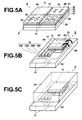
- FIG. 5A is a perspective view showing a light emitting diode, which acts as a fourth embodiment of the semiconductor light emitting device in accordance with the present invention.
- Figure 5B is a perspective view showing a semiconductor light emitting apparatus, which is provided with the light emitting diode of Figure 5A, with a sealing resin being omitted for clearness.
- Figure 5C is a perspective view showing the semiconductor light emitting apparatus of Figure 5B, with the sealing resin being illustrated.
- Figure 6 is a sectional view taken on line X-X' of Figure 5A.
- similar elements are numbered with the same reference numerals with respect to Figure 4A.
- this embodiment of a light emitting diode (a semiconductor light emitting device) 4 comprises an n-type (i.e., the first electrical conduction type) semiconductor base plate 11'.
- the light emitting diode 4 also comprises the n-type cladding layer 12, the non-doped lower light guiding layer 13 (not shown), the semiconductor active layer 14, the non-doped upper light guiding layer 15 (not shown), the p-type (i.e., the second electrical conduction type) cladding layer 16, the p-type contact layer 17 (not shown), and the p-type electrode 21, which are overlaid on the top surface of the n-type semiconductor base plate 11' and in this order from the side of the n-type semiconductor base plate 11'.
- the non-doped lower light guiding layer 13, the non-doped upper light guiding layer 15, and the p-type contact layer 17 reference may be made to Figure 4A.
- the semiconductor active layer 14 is a multiple quantum well active layer having a laminate structure comprising the quantum well layers 14A, 14A, ... and the barrier layers 14B, 14B, ..., which are overlaid alternately.
- the n-type semiconductor base plate 11' is constituted of the electrically conductive ZnO base plate and acts also as the n-type (i.e., the first electrical conduction type) electrode.
- the transition wavelengths of the plurality of the quantum well layers 14A, 14A, ... constituting the semiconductor active layer 14 are set to be different from one another, and the white light emission is thereby accomplished.
- the light emitting diode 4 comprises a plurality of light emitting sections 4A, 4B, 4C, and 4D, the center emission wavelengths of the light emitting sections 4A, 4B, 4C, and 4D are set to be different from one another, and the white light emission is thereby accomplished.
- the number of the light emitting sections is set at four. However, the number of the light emitting sections may be designed arbitrarily.
- the constitution itself of the light emitting diode, in which the plurality of the light emitting sections varying in center emission wavelength are provided, and in which the mixed light of the light having been produced by the light emitting sections is obtained, is the novel constitution.
- the n-type cladding layer 12 and the non-doped lower light guiding layer 13 are formed over the entire area of the surface of the n-type semiconductor base plate 11'. Also, the semiconductor active layer 14, the non-doped upper light guiding layer 15 (not shown), the p-type first cladding layer 16, the p-type contact layer 17 (not shown), and the p-type electrode 21 are formed in predetermined patterns on the non-doped lower light guiding layer 13 (not shown).
- the p-type electrodes 21, 21, 21, 21 of the light emitting sections 4A, 4B, 4C, and 4D are electrically isolated from one another.
- the semiconductor active layer 14 and the layers located on the side upward from the semiconductor active layer 14 are formed with a selective growth technique utilizing insulating film masks 23, 23, ...
- the opening rate of the insulating film masks 23, 23, ... is altered, and the area of the semiconductor active layer 14 is thereby altered.
- the insulating film masks 23, 23, ... are not formed, and the area of the light emitting section 4A and the area of the semiconductor active layer 14 coincide with each other.
- the insulating filmmasks 23, 23, ... are formed at each of the light emitting sections 4B, 4C, and 4D.
- the insulating filmmasks 23, 23, ... are formed such that the formation area of the insulating film masks 23, 23, ... becomes large (i.e., the opening rate of the insulating filmmasks 23, 23, ... becomes small) in the order of the light emitting section 4B, the light emitting section 4C, and the light emitting section 4D.
- the area of the semiconductor active layer 14 becomes small in the order of the light emitting section 4A, the light emitting section 4B, the light emitting section 4C, and the light emitting section 4D.
- the opening rate and the opening pattern of the insulating film masks 23, 23, ... are not limited to the examples illustrated in Figure 5A and may be designed arbitrarily.
- the crystal growth areas of the semiconductor active layer 14 and the layers located on the side upward from the semiconductor active layer 14 are determined by the opening rate of the insulating film masks 23, 23, ... Also, the crystal growth rate varies in accordance with the crystal growth area. Therefore, the thicknesses and the compositions of the semiconductor active layer 14 and the layers located on the side upward from the semiconductor active layer 14 are capable of being altered for each of the light emitting sections 4A, 4B, 4C, and 4D.
- the opening rate of the insulating film masks 23, 23, ... is varied for the light emitting sections 4A, 4B, 4C, and 4D.
- the area, the thickness, and the composition of the semiconductor active layer 14 are altered, and the center emission wavelengths of the light emitting sections 4A, 4B, 4C, and 4D are set at different values.
- the center emission wavelengths of the light emitting sections 4A, 4B, 4C, and 4D are capable of being varied.
- n-Type semiconductor base plate 11' Electrically conductive n-ZnO (0001) base plate
- the inventors have accomplished, for example, a center emission wavelength of 450nm (at the light emitting section 4A) / a center emission wavelength of 520nm (at the light emitting section 4B) / a center emission wavelength of 580nm (at the light emitting section 4C) / a center emission wavelength of 630nm (at the light emitting section 4D). Also, the inventors have accomplished the white light emission by the color mixing of the light emitted by the light emitting sections 4A, 4B, 4C, and 4D.
- each of the semiconductor layers ranging from the n-type cladding layer 12 to the p-type contact layer 17 is the semiconductor layer in accordance with the present invention, which has been formed with the laser assisted MOVPE technique.
- This embodiment of the light emitting diode 4 is constituted in the manner described above.
- This embodiment of the light emitting diode 4 is produced with the process, in which the ZnO base plate is used as the n-type semiconductor base plate 11', and in which the semiconductor layers 12 to 17, each of which is the AlGaInN layer or the GaInN layer, are formed on the n-type semiconductor base plate 11 by use of the laser assisted MOVPE technique.
- the AlGaInN layer or the GaInN layer is capable of being caused to grow on the n-type semiconductor base plate 11', such that the deterioration of the n-type semiconductor base plate 11' at the time of the production may be suppressed, and such that the formed layer may have good crystalline characteristics.
- the semiconductor active layer 14 in contrast with the technique proposed in, for example, Japanese Unexamined Patent Publication No. 1(1989)-017484 , the semiconductor active layer 14 has the multiple quantum well structure.
- the light emitting diode 4 in which the deterioration of the n-type semiconductor base plate 11' is capable of being suppressed, in which the semiconductor layers 12 to 17 have good crystalline characteristics, and in which the semiconductor active layer 14 has the multiple quantum well structure, by virtue of the effects of the features described above, the light emitting diode having a high efficiency and good light emission characteristics is capable of being obtained.
- the white light emitting diode With the constitution of this embodiment, it is possible to accomplish the white light emitting diode.
- the white light emitting diode in accordance with the present invention a markedly higher light emission efficiency is capable of being obtained, and electric power consumption is capable of being kept markedly lower than with the conventional white light emitting diode, in which the fluorescent substances are excited by the blue light emitting diode, in which the light having been produced by the blue light emitting diode and the light having been produced by the fluorescent substances are combined together, and in which the white light is thus obtained indirectly.
- This embodiment of the light emitting diode 4 also has the advantages of longer light emission life time over the conventional white light emitting diode, in which the fluorescent substances are excited by the blue light emitting diode, in which the light having been produced by the blue light emitting diode and the light having been produced by the fluorescent substances are combined together, and in which the white light is thus obtained indirectly.
- a ZnO base plate which is transparent with respect to visible light and which has high electric conductivity, is available commercially.
- the electrically conductive ZnO base plate is used as the n-type semiconductor base plate 11', and the n-type semiconductor base plate 11' acts also as the n-type electrode.
- an n-type SiC base plate or an n-type GaN base plate is ordinarily used. In such cases, it is essential to use an n-type electrode.
- the n-type electrodes include indium tin oxide (ITO), a very thin metal film, and a mesh-like metal film.
- ITO indium tin oxide
- the above-enumerated n-type electrodes are accompanied by slight loss and constitute a factor for lowering the light take-out efficiency.
- the n-type semiconductor base plate 11' acts also as the n-type electrode, the light take-out efficiency is capable of being kept higher than with the conventional light emitting diode provided with an n-type electrode.
- the ZnO base plate has the flat surface.
- recesses and protrusions should preferably be formed on the surface of the ZnO base plate.
- the recess and protrusion shapes on the surface of the ZnO base plate should preferably be of a moth-eye structure, in which small circular cone shapes or small pyramidal shapes stand side by side in an array pattern.
- the sizes of the recess and protrusion shapes on the surface of the ZnO base plate should preferably be approximately identical with wavelengths or smaller than the wavelengths.
- a semiconductor light emitting apparatus 5 comprises a mounting base plate 30 having a surface, on which electrodes 31, 31, wiring, and the like, have been formed in predetermined patterns.
- the semiconductor light emitting apparatus 5 also comprises the light emitting diode 4 described above, which has been mounted on a heat sink of the mounting base plate 30.
- This embodiment of the semiconductor light emitting apparatus 5 employs the so-called junction technique, in which the side of the p-type electrode 21 of the light emitting diode 4 is fusion bonded to the mounting base plate 30. Also, the n-type semiconductor base plate 11' of the light emitting diode 4, which base plate acts also as the n-type electrode, and the mounting base plate 30 are electrically connected with each other by bonding wires 33, 33, which may be gold wires, or the like.
- this embodiment of the semiconductor light emitting apparatus 5 is provided with a current control section 32 for controlling and optimizing the electric currents caused to flow across the light emitting sections 4A, 4B, 4C, and 4D.
- the current control section 32 comprises resistors 32A, 32B, 32C, and 32Dvarying in resistance value. Eachof the resistors 32A, 32B, 32C, and 32D is inserted in series between the electrodes 31, 31 and each of the light emitting sections 4A, 4B, 4C, and 4D.
- the electric current caused to flow across each of the light emitting sections 4A, 4B, 4C, and 4D is capable of being optimized by the current control section 32. Therefore, adjustment of the color temperature is capable of being performed. In accordance with the design conditions, it may often occur that the electric currents caused to flow across the light emitting sections 4A, 4B, 4C, and 4D should preferably be identical with one another. In such cases, by use of the current control section 32, the electric currents caused to flow across the light emitting sections 4A, 4B, 4C, and 4D are capable of being set to be identical with one another.
- This embodiment of the semiconductor light emitting apparatus 5 has the constitution, such that the electric currents caused to flow across the light emitting sections 4A, 4B, 4C, and 4D are controlled and optimized with the current control section 32 formed on the semiconductor light emitting apparatus 5.
- the constitution described above is convenient for preparation of commodity line-up. For example, in cases where commodity line-up varying in color temperature is to be prepared, the kinds of products of the semiconductor light emitting apparatus 5 need not be increased, and the resistors loaded on the semiconductor light emitting apparatus 5 may merely be altered for coping with different kinds of products.
- the feature described above is advantageous for keeping the cost low.
- the region of the semiconductor light emitting apparatus 5 other than the electrodes 31, 31 are sealed with a sealing resin 34 having the light transmissivity.
- This embodiment of the semiconductor light emitting apparatus 5 is constituted in the manner described above.
- the life time of the conventional white light emitting diodes is limited by the deterioration of the sealing resin. It has been thought that the deterioration of the sealing resin is caused to occur by blue light having high photon energy. Recently, the problems described above constitute detrimental problems for enhancement of the output of light emitting diodes. For the reasons of the problems described above, it is not always possible to apply the conventional white light emitting diodes in use applications for illumination, and the like. However, with this embodiment of the semiconductor light emitting apparatus 5, since the proportion of blue light emission is lower than with the conventional white light emitting diodes, the life time of the semiconductor light emitting apparatus 5 is capable of being kept long. Accordingly, this embodiment of the semiconductor light emitting apparatus 5 is advantageous also from the view point of the running cost.
- the present invention is not limited to the embodiments described above, and the device structures may be altered in various other ways.
- the layer compositions and the layer thicknesses were set as described above for the aforesaid embodiment of the semiconductor laser 1.
- An ArF excimer laser was used as the laser beam source 121, the output of the laser beam was set at 200mJ, and the pulse period was set at 100Hz.
- the laser beam having been radiated out from the laser beam source 121 was enlarged by the enlarging lens 122 and was then collimated by the collimator lens 123 into a collimated laser beam having a beam diameter of 2 inches.
- the laser beam L was thus irradiated to the base plate, such that the laser beam L might pass just above the base plate and in the direction parallel with the base plate surface.
- the irradiation of the laser beam L to the base plate was continued during the period of time from the beginning of the temperature rise of the base plate to the finish of the temperature fall of the base plate.
- the temperature of the base plate was set at 500°C.
- TMA/TEG/TMI were used.
- Group-V raw material ammonia was used.
- a hydrogen gas was introduced as a carrier gas into the reaction tube 110.
- SiH 4 silane
- a p-type dopant source Cp 2 Mg (bicyclopentadienylmagnesium) was used.
- the pressure in the reaction tube 110 was set at 20kPa.
- the SiO 2 insulating film 20 was formed in a predetermined pattern.
- the p-type electrode 21 was then formed with vacuum evaporation processing and heat treatment.
- the base plate 11 was then polished until the entire thickness of the device became equal to approximately 100 ⁇ m.
- the n-type electrode 22 was formed with the vacuum evaporation processing and the heat treatment. In this manner, the semiconductor laser 1 was obtained.
- the stripe width of the semiconductor laser 1 was set at 50 ⁇ m, and the resonator length was set at 500 ⁇ m.
- a dielectric multi-layer coating film having a reflectivity of 10% was formed on a front end face of the device. Also, a dielectric multi-layer coating film having a reflectivity of 90% was formed on a rear end face of the device.
- the device having thus been obtained was mounted with a junction down technique on a copper heat sink of a mounting base plate.
- the obtained device exhibited an external quantum efficiency of 10% and thus had a high efficiency.
- the wavelength of the produced laser beam was 520nm at the room temperature, and green light was obtained.
- the layer compositions and the layer thicknesses were set as described above for the aforesaid embodiment of the semiconductor laser 2.
- the resonator length was set at 300 ⁇ m.
- a dielectric multi-layer coating film having a reflectivity of 30% was formed on a front end face of the device. Also, a dielectric multi-layer coating film having a reflectivity of 60% was formed on a rear end face of the device.
- the device having thus been obtained was mounted with a junction up technique on an iron heat sink of a mounting base plate.
- the wavelength of the produced laser beam was 600nm at the room temperature, and yellow light was obtained.
- the layer compositions and the layer thicknesses were set as described above for the aforesaid embodiment of the light emitting diode 3.
- the fourGaInNquantumwell layers 14A, 14A, 14A, 14A constituting the semiconductor active layer 14 had an identical composition and had different thicknesses.
- the transition wavelengths of the quantum well layers 14A, 14A, 14A, 14A were set at 440nm/510nm/580nm/640nm in this order from the side of the base plate.
- the side of the p-type electrode 21 of the obtained device was mounted on an iron heat sink of a mounting base plate, such that the light might be taken out from the side of the n-type electrode 22.
- the light emission efficiency of the obtained light emitting diode was equal to 1201m/W.
- the light emission efficiency of the obtained light emitting diode was approximately three times as high as the light emission efficiency of the conventional white light emitting diode, in which the fluorescent substances are excited by the blue light emitting diode, in which the light having been produced by the blue light emitting diode and the light having been produced by the fluorescent substances are combined together, and in which the white light is thus obtained indirectly.
- the techniques in accordance with the present invention are capable of being applied appropriately to semiconductor light emitting devices, such as semiconductor lasers and light emitting diodes.
Landscapes
- Chemical & Material Sciences (AREA)
- Engineering & Computer Science (AREA)
- Crystallography & Structural Chemistry (AREA)
- Materials Engineering (AREA)
- Metallurgy (AREA)
- Organic Chemistry (AREA)
- Inorganic Chemistry (AREA)
- Chemical Kinetics & Catalysis (AREA)
- General Chemical & Material Sciences (AREA)
- Semiconductor Lasers (AREA)
- Led Devices (AREA)
Applications Claiming Priority (2)
| Application Number | Priority Date | Filing Date | Title |
|---|---|---|---|
| JP2006096879 | 2006-03-31 | ||
| JP2007042239A JP2007294878A (ja) | 2006-03-31 | 2007-02-22 | 半導体層とその成膜方法、半導体発光素子、及び半導体発光装置 |
Publications (3)
| Publication Number | Publication Date |
|---|---|
| EP1840979A2 true EP1840979A2 (de) | 2007-10-03 |
| EP1840979A3 EP1840979A3 (de) | 2010-10-20 |
| EP1840979B1 EP1840979B1 (de) | 2011-11-30 |
Family
ID=38069371
Family Applications (1)
| Application Number | Title | Priority Date | Filing Date |
|---|---|---|---|
| EP07006263A Expired - Fee Related EP1840979B1 (de) | 2006-03-31 | 2007-03-27 | Verfahren zur Herstellung einer Halbleiterschicht |
Country Status (4)
| Country | Link |
|---|---|
| US (1) | US7727791B2 (de) |
| EP (1) | EP1840979B1 (de) |
| JP (1) | JP2007294878A (de) |
| TW (1) | TWI407493B (de) |
Cited By (4)
| Publication number | Priority date | Publication date | Assignee | Title |
|---|---|---|---|---|
| CN101740600A (zh) * | 2008-11-18 | 2010-06-16 | Lg伊诺特有限公司 | 发光器件以及具有该发光器件的发光器件封装 |
| WO2011018411A1 (de) * | 2009-08-12 | 2011-02-17 | Osram Opto Semiconductors Gmbh | Strahlungsemittierendes halbleiterbauteil |
| WO2012059848A3 (en) * | 2010-11-02 | 2012-06-28 | Koninklijke Philips Electronics N.V. | Iii-nitride light emitting device |
| FR3112026A1 (fr) * | 2020-06-30 | 2021-12-31 | Aledia | Dispositif optoélectronique et procédé de fabrication |
Families Citing this family (4)
| Publication number | Priority date | Publication date | Assignee | Title |
|---|---|---|---|---|
| EP2200630B1 (de) * | 2007-09-28 | 2013-05-01 | Ut-Battelle, Llc | Nell1 zur behandlung von kardiovaskulärer erkrankungen |
| JP5801542B2 (ja) | 2010-07-13 | 2015-10-28 | 昭和電工株式会社 | 発光ダイオード及び発光ダイオードランプ |
| JP2013125847A (ja) * | 2011-12-14 | 2013-06-24 | Sumitomo Electric Ind Ltd | 受光素子、その製造方法、光学装置 |
| US10710116B2 (en) * | 2017-09-21 | 2020-07-14 | General Electric Company | Methods and systems for manufacturing an ultrasound probe |
Family Cites Families (18)
| Publication number | Priority date | Publication date | Assignee | Title |
|---|---|---|---|---|
| US4885260A (en) * | 1987-02-17 | 1989-12-05 | Matsushita Electric Industrial Co., Ltd. | Method of laser enhanced vapor phase growth for compound semiconductor |
| JPS6417484U (de) | 1988-05-09 | 1989-01-27 | ||
| JP3102647B2 (ja) * | 1990-12-10 | 2000-10-23 | 日本電信電話株式会社 | 半導体発光素子 |
| US5173751A (en) * | 1991-01-21 | 1992-12-22 | Pioneer Electronic Corporation | Semiconductor light emitting device |
| JP3557011B2 (ja) * | 1995-03-30 | 2004-08-25 | 株式会社東芝 | 半導体発光素子、及びその製造方法 |
| EP0772249B1 (de) * | 1995-11-06 | 2006-05-03 | Nichia Corporation | Halbleitervorrichtung aus einer Nitridverbindung |
| JPH11503879A (ja) * | 1995-12-21 | 1999-03-30 | フィリップス エレクトロニクス ネムローゼ フェンノートシャップ | 多色光放出ダイオード、その製造方法及びこのledが組み込まれた多色表示装置 |
| JPH11135838A (ja) * | 1997-10-20 | 1999-05-21 | Ind Technol Res Inst | 白色発光ダイオード及びその製造方法 |
| JPH11135436A (ja) * | 1997-10-29 | 1999-05-21 | Kyocera Corp | 化合物半導体膜の形成方法 |
| WO2000007221A2 (en) * | 1998-07-31 | 2000-02-10 | Emory University | Holographic, laser-induced fabrication of indium nitride quantum wires and quantum dots |
| JP3439179B2 (ja) * | 2000-07-28 | 2003-08-25 | 三菱重工業株式会社 | レーザーエッチング方法 |
| JP4374156B2 (ja) * | 2000-09-01 | 2009-12-02 | 日本碍子株式会社 | Iii−v族窒化物膜の製造装置及び製造方法 |
| US7229498B2 (en) * | 2002-10-29 | 2007-06-12 | Midwest Research Institute | Nanostructures produced by phase-separation during growth of (III-V)1-x(IV2)x alloys |
| JP2005210084A (ja) * | 2003-12-22 | 2005-08-04 | Ngk Insulators Ltd | エピタキシャル基板、半導体積層構造、転位低減方法およびエピタキシャル形成用基板 |
| JP2005303250A (ja) * | 2004-03-18 | 2005-10-27 | Matsushita Electric Ind Co Ltd | 半導体装置及びその製造方法 |
| JP2005268601A (ja) * | 2004-03-19 | 2005-09-29 | Sumitomo Chemical Co Ltd | 化合物半導体発光素子 |
| JP4864766B2 (ja) * | 2006-03-31 | 2012-02-01 | 富士フイルム株式会社 | 半導体層の成膜方法 |
| US20080132081A1 (en) * | 2006-12-04 | 2008-06-05 | Shaheen Mohamad A | Thin III-V semiconductor films with high electron mobility |
-
2007
- 2007-02-22 JP JP2007042239A patent/JP2007294878A/ja active Pending
- 2007-03-27 EP EP07006263A patent/EP1840979B1/de not_active Expired - Fee Related
- 2007-03-30 TW TW096111265A patent/TWI407493B/zh not_active IP Right Cessation
- 2007-04-02 US US11/730,459 patent/US7727791B2/en active Active
Non-Patent Citations (1)
| Title |
|---|
| YOSHIDA S. ET AL.: "GatnNP MQW structure LED grown by laser-assisted MOCVD", PHYSICA STATUS SOLIDI C, vol. 0, no. 7, 2003, pages 2236 - 2239 |
Cited By (8)
| Publication number | Priority date | Publication date | Assignee | Title |
|---|---|---|---|---|
| CN101740600A (zh) * | 2008-11-18 | 2010-06-16 | Lg伊诺特有限公司 | 发光器件以及具有该发光器件的发光器件封装 |
| EP2187442A3 (de) * | 2008-11-18 | 2010-12-29 | LG Innotek Co., Ltd. | Lichtemittierende Vorrichtung und lichtemittierende Vorrichtungsverpackung damit |
| WO2011018411A1 (de) * | 2009-08-12 | 2011-02-17 | Osram Opto Semiconductors Gmbh | Strahlungsemittierendes halbleiterbauteil |
| US9012926B2 (en) | 2009-08-12 | 2015-04-21 | Osram Opto Semiconductor Gmbh | Radiation-emitting semiconductor component |
| WO2012059848A3 (en) * | 2010-11-02 | 2012-06-28 | Koninklijke Philips Electronics N.V. | Iii-nitride light emitting device |
| US10304997B2 (en) | 2010-11-02 | 2019-05-28 | Lumileds Llc | III-nitride light emitting device with a region including only ternary, quaternary, and/or quinary III-nitride layers |
| FR3112026A1 (fr) * | 2020-06-30 | 2021-12-31 | Aledia | Dispositif optoélectronique et procédé de fabrication |
| WO2022002896A1 (fr) * | 2020-06-30 | 2022-01-06 | Aledia | Dispositif optoélectronique et procédé de fabrication correspondant |
Also Published As
| Publication number | Publication date |
|---|---|
| EP1840979A3 (de) | 2010-10-20 |
| EP1840979B1 (de) | 2011-11-30 |
| JP2007294878A (ja) | 2007-11-08 |
| TWI407493B (zh) | 2013-09-01 |
| US7727791B2 (en) | 2010-06-01 |
| US20070228394A1 (en) | 2007-10-04 |
| TW200802551A (en) | 2008-01-01 |
Similar Documents
| Publication | Publication Date | Title |
|---|---|---|
| CN100438088C (zh) | 制造发光装置的方法 | |
| EP1840979A2 (de) | Halbleiterschicht, Verfahren zu deren Herstellung und lichtemittierendes Halbleiterbauelement | |
| US9595813B2 (en) | Laser package having multiple emitters configured on a substrate member | |
| EP1754265B1 (de) | Led mit leuchtstoff | |
| JP4864766B2 (ja) | 半導体層の成膜方法 | |
| US7998773B2 (en) | Method of growing semiconductor heterostructures based on gallium nitride | |
| JP2001160627A (ja) | Iii族窒化物系化合物半導体発光素子 | |
| EP2037508A1 (de) | Zno-basiertes halbleiterelement | |
| KR100752007B1 (ko) | 3족 질화물계 화합물 반도체 발광 소자 및 그 제조 방법 | |
| JP2008227002A (ja) | 窒化物半導体レーザ素子 | |
| US20100259184A1 (en) | Light-emitting device | |
| JP3424465B2 (ja) | 窒化物半導体素子及び窒化物半導体の成長方法 | |
| WO2009142265A1 (ja) | Iii族窒化物半導体発光素子及びその製造方法、並びにランプ | |
| JPH11340505A (ja) | 窒化ガリウム系化合物半導体発光素子 | |
| CN101454908A (zh) | 发光元件及其制造方法 | |
| JP5075298B1 (ja) | 窒化物系半導体発光素子およびその製造方法 | |
| JP2000183466A (ja) | 化合物半導体レーザおよびその製造方法 | |
| JP4145108B2 (ja) | GaNP結晶の成長方法 | |
| JP5158834B2 (ja) | 半導体発光素子および半導体発光素子の製造方法 | |
| JPH09289352A (ja) | 半導体レーザ装置およびその製造方法 | |
| JP4567896B2 (ja) | 半導体発光素子の製造方法 | |
| JP3211383B2 (ja) | 半導体多層膜反射鏡の製造方法 | |
| JP2003046203A (ja) | 窒化物半導体の成長方法 | |
| JP2006019713A (ja) | Iii族窒化物半導体発光素子およびそれを用いたled | |
| JPH05347431A (ja) | 半導体素子用基板および半導体素子 |
Legal Events
| Date | Code | Title | Description |
|---|---|---|---|
| PUAI | Public reference made under article 153(3) epc to a published international application that has entered the european phase |
Free format text: ORIGINAL CODE: 0009012 |
|
| AK | Designated contracting states |
Kind code of ref document: A2 Designated state(s): AT BE BG CH CY CZ DE DK EE ES FI FR GB GR HU IE IS IT LI LT LU LV MC MT NL PL PT RO SE SI SK TR |
|
| AX | Request for extension of the european patent |
Extension state: AL BA HR MK YU |
|
| PUAL | Search report despatched |
Free format text: ORIGINAL CODE: 0009013 |
|
| AK | Designated contracting states |
Kind code of ref document: A3 Designated state(s): AT BE BG CH CY CZ DE DK EE ES FI FR GB GR HU IE IS IT LI LT LU LV MC MT NL PL PT RO SE SI SK TR |
|
| AX | Request for extension of the european patent |
Extension state: AL BA HR MK RS |
|
| 17P | Request for examination filed |
Effective date: 20110419 |
|
| REG | Reference to a national code |
Ref country code: DE Ref legal event code: R079 Ref document number: 602007019000 Country of ref document: DE Free format text: PREVIOUS MAIN CLASS: H01L0033000000 Ipc: H01L0021205000 |
|
| AKX | Designation fees paid |
Designated state(s): DE FR GB |
|
| GRAP | Despatch of communication of intention to grant a patent |
Free format text: ORIGINAL CODE: EPIDOSNIGR1 |
|
| RIC1 | Information provided on ipc code assigned before grant |
Ipc: H01S 5/343 20060101ALN20110610BHEP Ipc: H01L 21/205 20060101AFI20110610BHEP Ipc: H01L 33/32 20100101ALN20110610BHEP Ipc: C30B 25/10 20060101ALI20110610BHEP Ipc: H01L 27/15 20060101ALN20110610BHEP Ipc: C30B 29/40 20060101ALI20110610BHEP |
|
| RTI1 | Title (correction) |
Free format text: PROCESS FOR FORMING A SEMICONDUCTOR LAYER |
|
| GRAS | Grant fee paid |
Free format text: ORIGINAL CODE: EPIDOSNIGR3 |
|
| GRAA | (expected) grant |
Free format text: ORIGINAL CODE: 0009210 |
|
| AK | Designated contracting states |
Kind code of ref document: B1 Designated state(s): DE FR GB |
|
| REG | Reference to a national code |
Ref country code: GB Ref legal event code: FG4D |
|
| REG | Reference to a national code |
Ref country code: DE Ref legal event code: R096 Ref document number: 602007019000 Country of ref document: DE Effective date: 20120202 |
|
| REG | Reference to a national code |
Ref country code: DE Ref legal event code: R082 Ref document number: 602007019000 Country of ref document: DE Representative=s name: KLUNKER, SCHMITT-NILSON, HIRSCH, DE |
|
| REG | Reference to a national code |
Ref country code: DE Ref legal event code: R081 Ref document number: 602007019000 Country of ref document: DE Owner name: NICHIA CORP., JP Free format text: FORMER OWNER: FUJIFILM CORPORATION, TOKIO/TOKYO, JP Effective date: 20120521 Ref country code: DE Ref legal event code: R081 Ref document number: 602007019000 Country of ref document: DE Owner name: NICHIA CORP., JP Free format text: FORMER OWNER: FUJIFILM CORP., TOKIO/TOKYO, JP Effective date: 20111208 Ref country code: DE Ref legal event code: R082 Ref document number: 602007019000 Country of ref document: DE Representative=s name: KLUNKER, SCHMITT-NILSON, HIRSCH, DE Effective date: 20120521 Ref country code: DE Ref legal event code: R081 Ref document number: 602007019000 Country of ref document: DE Owner name: NICHIA CORP., ANAN-SHI, JP Free format text: FORMER OWNER: FUJIFILM CORP., TOKIO/TOKYO, JP Effective date: 20111208 Ref country code: DE Ref legal event code: R081 Ref document number: 602007019000 Country of ref document: DE Owner name: NICHIA CORP., ANAN-SHI, JP Free format text: FORMER OWNER: FUJIFILM CORPORATION, TOKIO/TOKYO, MINATO-KU, JP Effective date: 20120521 |
|
| REG | Reference to a national code |
Ref country code: GB Ref legal event code: 732E Free format text: REGISTERED BETWEEN 20120621 AND 20120627 |
|
| REG | Reference to a national code |
Ref country code: FR Ref legal event code: TP Owner name: NICHIA CORPORATION, JP Effective date: 20120806 |
|
| PLBE | No opposition filed within time limit |
Free format text: ORIGINAL CODE: 0009261 |
|
| STAA | Information on the status of an ep patent application or granted ep patent |
Free format text: STATUS: NO OPPOSITION FILED WITHIN TIME LIMIT |
|
| 26N | No opposition filed |
Effective date: 20120831 |
|
| REG | Reference to a national code |
Ref country code: DE Ref legal event code: R097 Ref document number: 602007019000 Country of ref document: DE Effective date: 20120831 |
|
| REG | Reference to a national code |
Ref country code: FR Ref legal event code: PLFP Year of fee payment: 9 |
|
| PGFP | Annual fee paid to national office [announced via postgrant information from national office to epo] |
Ref country code: DE Payment date: 20150324 Year of fee payment: 9 |
|
| PGFP | Annual fee paid to national office [announced via postgrant information from national office to epo] |
Ref country code: FR Payment date: 20150309 Year of fee payment: 9 Ref country code: GB Payment date: 20150325 Year of fee payment: 9 |
|
| REG | Reference to a national code |
Ref country code: DE Ref legal event code: R119 Ref document number: 602007019000 Country of ref document: DE |
|
| GBPC | Gb: european patent ceased through non-payment of renewal fee |
Effective date: 20160327 |
|
| REG | Reference to a national code |
Ref country code: FR Ref legal event code: ST Effective date: 20161130 |
|
| PG25 | Lapsed in a contracting state [announced via postgrant information from national office to epo] |
Ref country code: FR Free format text: LAPSE BECAUSE OF NON-PAYMENT OF DUE FEES Effective date: 20160331 Ref country code: DE Free format text: LAPSE BECAUSE OF NON-PAYMENT OF DUE FEES Effective date: 20161001 Ref country code: GB Free format text: LAPSE BECAUSE OF NON-PAYMENT OF DUE FEES Effective date: 20160327 |