EP1829113B1 - Normally-off integrated jfet power switches in wide bandgap semiconductors - Google Patents
Normally-off integrated jfet power switches in wide bandgap semiconductors Download PDFInfo
- Publication number
- EP1829113B1 EP1829113B1 EP05849440A EP05849440A EP1829113B1 EP 1829113 B1 EP1829113 B1 EP 1829113B1 EP 05849440 A EP05849440 A EP 05849440A EP 05849440 A EP05849440 A EP 05849440A EP 1829113 B1 EP1829113 B1 EP 1829113B1
- Authority
- EP
- European Patent Office
- Prior art keywords
- layer
- region
- drain
- semiconductor material
- jfet
- Prior art date
- Legal status (The legal status is an assumption and is not a legal conclusion. Google has not performed a legal analysis and makes no representation as to the accuracy of the status listed.)
- Expired - Lifetime
Links
Images


Classifications
-
- H—ELECTRICITY
- H03—ELECTRONIC CIRCUITRY
- H03K—PULSE TECHNIQUE
- H03K17/00—Electronic switching or gating, i.e. not by contact-making and –breaking
- H03K17/51—Electronic switching or gating, i.e. not by contact-making and –breaking characterised by the components used
- H03K17/56—Electronic switching or gating, i.e. not by contact-making and –breaking characterised by the components used by the use, as active elements, of semiconductor devices
- H03K17/567—Circuits characterised by the use of more than one type of semiconductor device, e.g. BIMOS, composite devices such as IGBT
-
- H—ELECTRICITY
- H10—SEMICONDUCTOR DEVICES; ELECTRIC SOLID-STATE DEVICES NOT OTHERWISE PROVIDED FOR
- H10D—INORGANIC ELECTRIC SEMICONDUCTOR DEVICES
- H10D48/00—Individual devices not covered by groups H10D1/00 - H10D44/00
- H10D48/30—Devices controlled by electric currents or voltages
- H10D48/32—Devices controlled by only the electric current supplied, or only the electric potential applied, to an electrode which does not carry the current to be rectified, amplified or switched
- H10D48/36—Unipolar devices
-
- H—ELECTRICITY
- H10—SEMICONDUCTOR DEVICES; ELECTRIC SOLID-STATE DEVICES NOT OTHERWISE PROVIDED FOR
- H10D—INORGANIC ELECTRIC SEMICONDUCTOR DEVICES
- H10D30/00—Field-effect transistors [FET]
- H10D30/80—FETs having rectifying junction gate electrodes
- H10D30/83—FETs having PN junction gate electrodes
- H10D30/831—Vertical FETs having PN junction gate electrodes
-
- H—ELECTRICITY
- H10—SEMICONDUCTOR DEVICES; ELECTRIC SOLID-STATE DEVICES NOT OTHERWISE PROVIDED FOR
- H10D—INORGANIC ELECTRIC SEMICONDUCTOR DEVICES
- H10D30/00—Field-effect transistors [FET]
- H10D30/80—FETs having rectifying junction gate electrodes
- H10D30/83—FETs having PN junction gate electrodes
- H10D30/832—Thin-film junction FETs [JFET]
-
- H—ELECTRICITY
- H10—SEMICONDUCTOR DEVICES; ELECTRIC SOLID-STATE DEVICES NOT OTHERWISE PROVIDED FOR
- H10D—INORGANIC ELECTRIC SEMICONDUCTOR DEVICES
- H10D8/00—Diodes
-
- H—ELECTRICITY
- H10—SEMICONDUCTOR DEVICES; ELECTRIC SOLID-STATE DEVICES NOT OTHERWISE PROVIDED FOR
- H10D—INORGANIC ELECTRIC SEMICONDUCTOR DEVICES
- H10D8/00—Diodes
- H10D8/50—PIN diodes
-
- H—ELECTRICITY
- H10—SEMICONDUCTOR DEVICES; ELECTRIC SOLID-STATE DEVICES NOT OTHERWISE PROVIDED FOR
- H10D—INORGANIC ELECTRIC SEMICONDUCTOR DEVICES
- H10D8/00—Diodes
- H10D8/60—Schottky-barrier diodes
-
- H—ELECTRICITY
- H10—SEMICONDUCTOR DEVICES; ELECTRIC SOLID-STATE DEVICES NOT OTHERWISE PROVIDED FOR
- H10D—INORGANIC ELECTRIC SEMICONDUCTOR DEVICES
- H10D84/00—Integrated devices formed in or on semiconductor substrates that comprise only semiconducting layers, e.g. on Si wafers or on GaAs-on-Si wafers
- H10D84/80—Integrated devices formed in or on semiconductor substrates that comprise only semiconducting layers, e.g. on Si wafers or on GaAs-on-Si wafers characterised by the integration of at least one component covered by groups H10D12/00 or H10D30/00, e.g. integration of IGFETs
- H10D84/87—Integrated devices formed in or on semiconductor substrates that comprise only semiconducting layers, e.g. on Si wafers or on GaAs-on-Si wafers characterised by the integration of at least one component covered by groups H10D12/00 or H10D30/00, e.g. integration of IGFETs of PN-junction gate FETs
-
- H—ELECTRICITY
- H10—SEMICONDUCTOR DEVICES; ELECTRIC SOLID-STATE DEVICES NOT OTHERWISE PROVIDED FOR
- H10D—INORGANIC ELECTRIC SEMICONDUCTOR DEVICES
- H10D62/00—Semiconductor bodies, or regions thereof, of devices having potential barriers
- H10D62/80—Semiconductor bodies, or regions thereof, of devices having potential barriers characterised by the materials
- H10D62/83—Semiconductor bodies, or regions thereof, of devices having potential barriers characterised by the materials being Group IV materials, e.g. B-doped Si or undoped Ge
- H10D62/832—Semiconductor bodies, or regions thereof, of devices having potential barriers characterised by the materials being Group IV materials, e.g. B-doped Si or undoped Ge being Group IV materials comprising two or more elements, e.g. SiGe
- H10D62/8325—Silicon carbide
-
- H—ELECTRICITY
- H10—SEMICONDUCTOR DEVICES; ELECTRIC SOLID-STATE DEVICES NOT OTHERWISE PROVIDED FOR
- H10D—INORGANIC ELECTRIC SEMICONDUCTOR DEVICES
- H10D62/00—Semiconductor bodies, or regions thereof, of devices having potential barriers
- H10D62/80—Semiconductor bodies, or regions thereof, of devices having potential barriers characterised by the materials
- H10D62/85—Semiconductor bodies, or regions thereof, of devices having potential barriers characterised by the materials being Group III-V materials, e.g. GaAs
- H10D62/8503—Nitride Group III-V materials, e.g. AlN or GaN
Definitions
- the present invention relates generally to field effect transistors (FETs), and in particular, to such transistors formed in wide bandgap semiconductor materials. Further, this invention relates to monolithic and hybrid integrated circuits comprising low-voltage control circuitry and to power switches built using the above transistors.
- FETs field effect transistors
- monolithic and hybrid integrated circuits comprising low-voltage control circuitry and to power switches built using the above transistors.
- Wide bandgap semiconductor materials such as silicon carbide (SiC) or Group III nitride compound semiconductors (e.g. , gallium nitride or GaN) are very attractive for use in high-power, high-temperature, and/or radiation resistant electronics.
- SiC silicon carbide
- Group III nitride compound semiconductors e.g. , gallium nitride or GaN
- Monolithic or hybrid integration of a power transistor and control circuitry in a single or multi-chip wide bandgap power semiconductor module is highly desirable for such applications in order to improve the efficiency and reliability of the system.
- SiC smart power technology has been a topic of discussion in recent years, but has experienced limited scientific investigation. Proposed solutions have been met with skepticism relating to the operation of both the power switch and control circuitry.
- CMOS Complementary Metal-Oxide-Semiconductor
- DCFL Direct Coupled FET Logic
- MOSFETs SiC Lateral DMOS Field-Effect Transistors
- LDMOSFETs SiC Lateral DMOS Field-Effect Transistors
- Various issues limit the use of MOSFET-based SiC integrated circuits in the applications where high-temperature and/or radiation tolerance is required.
- the first such issue is on-state insulator reliability as a result of a much smaller conduction band offset of SiC to SiO 2 as compared to that of silicon. This issue becomes even more significant at high temperatures and in extreme radiation environments.
- Other issues include: low inversion channel mobility due to high interface state density at the SiC/SiO 2 interface and high fixed charge density in the insulator; and significant threshold voltage shift with temperature due to ionization of interface states.
- SiC bipolar junction transistor Another transistor candidate for use in SiC Smart Power electronics, a SiC bipolar junction transistor (BJT), also suffers from interface-related issues such as high recombination velocity on the surface between the emitter and the base resulting in low current gain and high control losses.
- SiC MESFET Metal Semiconductor Field-Effect Transistor
- VJFET switches Several attempts to build normally-off SiC high-voltage VJFET switches have been reported recently. Typically, these devices comprise both lateral and vertical channel regions (e.g ., [10]-[12]). These devices, however, exhibit a drastic contradiction between the device blocking capabilities and the specific on-resistance. For example, a VJFET with a 75 ⁇ m, 7x10 14 cm -3 n-type drift region was able to block above 5.5 kV at zero gate-to-source voltage [13].
- this device demonstrated a specific on-resistance (R sp-on ) of more then 200 m ⁇ *cm 3 .
- the intrinsic resistance of its drift layer estimated from its thickness and doping was slightly above 60 m ⁇ *cm 3 , with the remainder of the on-resistance was contributed by the channel regions.
- these devices can be driven in bipolar mode by applying high positive gate-to-source voltage.
- the device discussed above and disclosed in [13] demonstrated an R sp-on of 66.7 m ⁇ *cm 3 when a gate-to-source bias of 5 V was applied [14]. This approach, however, can lead to significant power losses due to high gate current.
- a cascode connection of a low-voltage control JFET with a high-voltage JFET wherein the drain of the control JFET is connected to the source of the high-voltage device and the gate of high-voltage JFET is connected to the source of the control JFET has been disclosed in U.S. Patent No. 3,767,946 [15].
- a compound field-effect transistor monolithically implementing such a cascode connection has also been disclosed in U.S. Patent No. 4,107,725 [16].
- Similar types of cascode circuits, where low-voltage normally-off devices control high-voltage normally-on devices are disclosed in U.S. Patent No.
- JP 59147467 describes a static induction transistor in which a drain region, channel region and source region are formed on an insulating semiconductor substrate and a p type gate region is formed in the channel region.
- WO 02/37200 describes a circuit comprising a first JFET connected in series to a second JFET with a gate of a first JFET connected to a source of the second JFET and to a load and not to ground.
- the gate of the second JFET is connected to ground.
- the JFETs may be formed by silicon on insulator integration technology.
- JP 2002076020 describes a normally-off-type JFET and a normally-on-type JFET combined with each other with the source electrode of the normally-off-type JFET connected with the gate electrode of the normally-on-type JFET and the drain electrode of the normally-off-type JFET connected with the source electrode of the normally-on-type JFET.
- Described herein is a monolithic integrated circuit which comprises:
- Described herein is an integrated circuit which comprises:
- Described herein is an integrated circuit which comprises:
- JFET monolithic lateral channel junction field-effect transistor
- Described herein is an integrated circuit which comprises:
- a monolithic integrated circuit which comprises a lateral junction field effect transistor and a vertical junction field effect transistor; the lateral junction field effect transistor comprising:
- a monolithic integrated circuit which comprises a lateral junction field effect transistor and a vertical junction field effect transistor; the lateral junction field effect transistor comprising:
- SiC silicon carbide
- Silicon carbide crystallizes in numerous (i.e., more than 200) different modifications (polytypes). The most important are: 3C-SiC (cubic unit cell, zincblende); 2H-SiC; 4H-SiC; 6H-SiC (hexagonal unit cell, wurtzile); 15R-SiC (rhombohedral unit cell).
- the 4H polytype is more attractive for power devices, because of its higher electron mobility.
- the 4H-SiC is preferred, it is to be understood that the present invention is applicable to devices and integrated circuits described herein made of other wide bandgap semiconductor materials such as gallium nitride, and other polytypes of silicon carbide, by way of example.
- FIG. 1 shows a schematic cross-section of enhanced and depletion mode semiconductor devices referred to a Lateral Trench Junction Field-Effect Transistors (LTJFETs), and a schematic presentation of electrical connections used to form a monolithic inverter circuit.
- the devices used to form the inverter are built on a wide bandgap semiconductor substrate (1), which can be either: semi-insulating; p-type; or n-type with a p-type buffer layer.
- the devices comprise drain (3), drift (4), channel (5), and source (6) expitaxially grown n-type layers, and p-type implanted gate regions (7).
- the device structures can be defined using plasma etching and ion implantation.
- the ohmic contacts to the source, gate, and drain regions can be formed on the same side of the wafer, which allows for the devices to be used in monolithic integrated circuits.
- a complete description of a device as described above and shown in Figure 1 as well as an exemplary fabrication method for this device can be found in U.S. Patent Application Serial No. 10/999,954 , entitled: "Lateral Trench Field-Effect Transistors in Wide Bandgap Semiconductor Materials, methods of Making, and Integrated Circuits Incorporating the Transistors", filed on even date herewith.
- FIG. 2 is a schematic representation of a monolithic normally-off JFET comprising single-finger enhanced and depletion mode LTJFETs and having a built-in PiN diode.
- a schematic presentation of electrical connections is also shown in Figure 2 .
- the devices are connected in cascode configuration in such a way that the drain of the enhanced mode transistor (referred to as an "EJFET”) is connected to the source of the depletion mode transistor (referred to as a "DJFET”), and the gate of the DJFET is connected to the source of the control EJFET.
- EJFET enhanced mode transistor
- DJFET depletion mode transistor
- the p-n junctions formed in between the gate regions (7) and the drift layer (4) of the DJFET of this device form a so called anti-parallel free-wheeling PiN diode.
- the size of this diode can be defined by the widths of implanted gate regions.
- Figure 2 shows single-finger device implementation of a normally-off JFET
- multi-finger LTJFETs can be used to form power switches.
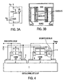
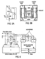
- Figures 3A and 3B shows a schematic circuit representation ( Figure 3A ) and an exemplary layout design ( Figure 3B ) of a monolithic multi-finger normally-off power switch.
- the PiN diode shown as in Figures 3A and 3B can be replaced with a Schottky Barrier diode (SBD) or a Junction Barrier Schottky (JBS) diode.
- SBD Schottky Barrier diode
- JBS Junction Barrier Schottky
- Methods of forming Schottky gates in a trench structure are disclosed in U.S. Patent Application No. 60/585,881, filed July 8, 2004 .
- Figure 4 provides a schematic cross-section of a monolithic normally-off JFET power switch with an integrated free-wheeling SBD or JBS diode
- Figures 5A and 5B provide a schematic circuit representation ( Figure 5A ) and exemplary layout design ( Figure 5B ) of such a switch monolithically formed using multi-finger LTJFETs.
- Figures 6 and 7 are schematic cross-sectional representations of single-finger normally-off JFET power switches where enhancement-mode low-voltage LTJFETs control high-voltage discrete normally-on depletion-mode VJFETs.
- Figure 6 shows a hybrid JFET power switch with a built-in anti-parallel PiN diode
- Figure 7 shows a JFET power switch comprising an anti-parallel SBD or JBS diode monolithically integrated with a high-voltage VJFET.
- a monolithic LTJFET timer circuit drives a built-on-chip low-voltage high-current enhanced-mode LTJFET connected in cascode with a discrete high-voltage normally-on power VJFET.
- FIGS. 9-17 illustrate various exemplary embodiments of integrated JFET switches built using enhanced and depletion mode Lateral Junction Field-Effect Transistors (LJFETs).
- LJFETs Lateral Junction Field-Effect Transistors
- Figure 9 is a schematic cross-sectional representation with electrical connections of a lateral channel JFET integrated circuit comprising enhanced and depletion mode LJFETs having expitaxially overgrown gates.
- the integrated circuit forms a monolithic inverter circuit.
- the LJFETs used to form the inverter are built on the wide bandgap semiconductor substrate (1), which can be either: semi-insulating; p-type; or n-type with a p-type buffer layer.
- the integrated circuit comprises buffer (2) and channel (5a) epitaxially grown n-type layers, as well as implanted source and drain (6a) regions and expitaxially grown p-type gate regions (7a).
- the device structures can be defined using plasma etch and ion implantation.
- the ohmic contacts (8) to the source, gate, and drain regions can be formed on the same side of the wafer allowing for the use of the device in monolithic integrated circuits.
- Figure 10 is a schematic representation of a pitch of a monolithic normally-off JFET power switch built using enhanced and depletion mode LJFETs with overgrown gate regions.
- the devices are connected in cascode configuration in such a way that the drain of the low-voltage enhanced mode LJFET (referred to as an "ELJFET”) is connected to the source of the higher-voltage depletion mode LJFET (referred to as a "DLJFET”), and the gate of the DLJFET is connected to the source of the control ELJFET.
- ELJFET low-voltage enhanced mode LJFET
- DLJFET higher-voltage depletion mode LJFET
- Figure 11 shows a schematic cross-section of a hybrid normally-off JFET power switch wherein a low-voltage ELJFET controls a high-voltage discrete normally-on depletion-mode VJFET.
- LJFET structure where source and drain regions are formed in an epitaxially grown n-type layer and gate regions are defined by ion implantation can also be used. Devices of this type are shown in Figures 12-17 .
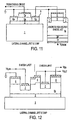
- Figure 12 shows is a schematic cross-sectional representation with electrical connections of a monolithic inverter circuit comprising enhanced and depletion mode implanted-gate LJFETs.
- the devices used to form the inverter are built on a wide bandgap semiconductor substrate (1), which can be either: semi-insulating; p-type; or n-type with a p-type buffer layer.
- the device comprises buffer (2), channel (5b), source and drain (6) epitaxially grown n-type layers, as well as implanted gate (7) regions.
- Figure 13 is a schematic cross-sectional representation of a pitch of a monolithic normally-off JFET power switch built using enhanced and depletion mode implanted-gate LJFETs. As shown in Figure 13 , the drain of the D-mode LJFET is laterally spaced from the gate on the channel layer (5b) to form a lateral drift region in the device.
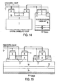
- Figure 14 is a schematic cross-sectional representation of a normally-off JFET power switch where an enhancement-mode low-voltage implanted-gate LJFET controls a high-voltage discrete normally-on depletion-mode VJFET.
- Figure 15 is a schematic cross-sectional representation of a monolithic normally-off JFET power switch wherein an enhancement-mode low-voltage dual-gate LJFET controls a high-voltage discrete normally-on depletion-mode VJFET. As shown in Figure 15 , the bottom gate of the LJFET is implanted into drift region (4) before the channel region is grown thereon.
- Figure 16 is a schematic cross-sectional representation of a device as shown in Figure 3D wherein the bottom gate of the LJFET is implanted into drift region 4 together with guard rings.
- the guard rings can be used to increase the voltage blocking capability of the switch.
- FIG 17 is a schematic cross-sectional representation of a device as shown in Figure 16 wherein the implanted p-type top gate of the LJFET and the implanted gate of the discrete normally-on depletion-mode VJFET are replaced with Schottky gates.
- the Schottky gate of the discrete normally-on FET also serves as an integrated anti-parallel free-wheeling diode.
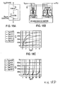
- Figures 18A-18D shows a simulated device structure ( Figure 18A ), schematic cross-sectional representation ( Figure 18B ) and graphs showing the output DC characteristics ( Figures 18C and 18D ) of a SiC LTJFET integrated switch, where both the EJFET and the DJFET have channel peripheries of 1 cm.
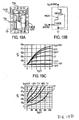
- FIGS 19A-19D are a photograph ( Figure 19A ), a schematic representation ( Figure 19B ) and graphs showing measured characteristics ( Figures 19C and 19D ) of a hybrid normally-off, 900 V power switch.
- the voltage-controlled SiC power switch was controlled by as little as 2.75 V.
- VGS the enhanced mode transistor
- the specific on-resistance of the integrated switch can be minimized as follows. First, the ratios of pinch-off voltages and channel peripheries of both transistors (e.g ., EJFET and DJFET) can be adjusted so that they will have approximately equal on-resistances and neither one will therefore limit the overall current. Second, the device can be constructed such that the gate-to-source breakdown voltage of DJFET is equal or higher than the drain-to-source breakdown voltage of EJFET.
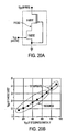
- FIGS 21A and 21B are schematic representations of distributed drain resistances of LTJFET ( Figure 21 A) and VJFET ( Figure 21B ), and graph ( Figure 21 C) showing resistance of the lateral drain layer of LTJFET normalized to the resistance of the vertical drain of VJFET as a function of finger length for different dopings of the lateral drain layer.
- the finger length of the LTJFET will preferably not exceed 100 ⁇ m in length. The finger length, however, can be increased by increasing the thickness and/or the doping levels of the drain layer (3).
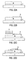
- Figures 22A-22H illustrate a method of making a device as set forth in Figure 9 .
- Figure 22A shows a multi-layer structure comprising a substrate (1), an epitaxially grown p-type layer (2), and an epitaxially grown n-type layer (5a).
- An etch mask (10) is positioned on the exposed surface of epitaxially grown n-type layer (5a) as shown in Figure 22B .
- Epitaxially grown n-type layer (5a) is then selectively etched (12) as shown in Figure 22B .
- Etch mask (10) is then removed and ion implantation mask (14) is then placed on the etched surface of epitaxially grown n-type layer (5a) as shown in Figure 22D .
- Ion implantation of n-type dopants through mask (14) results in the formation of highly n-doped regions (6a) in epitaxially grown n-type layer (5a) as shown in Figure 22E .
- Mask (14) is then removed and a layer of p-type semiconductor material (7a) is grown on the etched and implanted surface of epitaxially grown n-type layer (5a) as shown in Figure 22F .
- Etch mask (16) is then positioned on the exposed surface of layer (7a) as shown in Figure 22G .
- Etching through mask (16) results in selective removal of layer (7a) and formation of raised p-type features as also shown in Figure 22G .
- mask (16) is removed and ohmic contacts are formed on exposed surfaces of the raised p-type features and the implanted regions (6a).
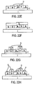
- Figures 23A-23H illustrate a method of making a structure as shown in Figure 12 .
- Figure 23A shows a substrate (1), an epitaxially grown p-type layer (2) on the substrate (1), and an epitaxially grown n-type layer (5b) on layer (2).
- an etch mask (18) is positioned on the exposed surface of layer (5b).
- Etching (20) results in selective removal of material from layer (5b) as shown in Figure 23C .
- an n-type epitaxial layer (6) is grown on the etched surface of layer (5b) as shown in Figure 23D .
- Etch mask (22) is positioned on the exposed surface of layer (6) as shown in Figure 23E and etching (24) results in selective removal of material from layer (6) and exposure of underlying layer (5b) as shown in Figure 23F .
- Mask (22) is then used to selectively implant p-type donors in exposed surface of layer (5b) to form implanted gate regions (7) as shown in Figure 23G .
- Ohmic contacts (8) are then formed on the implanted p-type gate regions (7) to form the gate contacts and on the raised n-type regions (6) to form the source and drain contacts for the device as shown in Figure 23H .
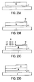
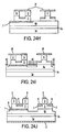
- Figures 24A-24J illustrate a method of making a structure as shown in Figure 15 .
- Figure 24A shows an n-type substrate (1a), an epitaxially grown n-type layer (3a) on substrate (1a), and an epitaxially grown n-type layer (4a) on layer (3a).
- An ion implantation mask (26) is also shown on the exposed upper surface of layer (4a).
- layer (4a) is selectively implanted with p-type donor atoms through mask (26) to form gate region (7).
- an n-type epitaxial layer (5) and an n-type epitaxial layer (6) are successively grown on the implanted surface of layer (4a) as shown in Figures24C and 24D .
- Etch mask (30) is then positioned on the exposed surface of layer (6) as shown in Figure 24D followed by etching (31) through layer (6) and partially through underlying layer (5) ( Figure 24E ). Exposed portions of layer (5) are then implanted with p-type donor atoms through mask (30) to form additional gate regions (7) as shown in Figure 24F .
- Etch mask (34) is then positioned on the surface of the etched and implanted structure and etching (36) results in selective removal of portions of layer (5) including portions of the p-type implanted gate regions ( Figure 24H ). Exposed portions of layer (4a) are then etched (40) thorugh mask (38) as shown in Figure 24I . Ohmic contacts (8) are then formed on the etched and implanted structure to form the device as shown in Figure 24J .
- the method as outlined above can also be used to form a structure as shown in Figure 16 .
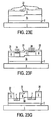
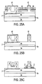
- FIGs 25A-25D illustrate a method of making a structure as shown in Figure 17 .
- a structure a shown in Figure 24E is etched (44) through mask (42) to expose portions of underlying layer (4a) ( Figure 25B ).
- Schottky contacts (9) are then formed on the etched/implanted structure as shown in Figure 25C .
- the formation of ohmic contacts (8) results in the device as shown in Figure 25D .
- GaN n-type epitaxial layers can be grown on silicon carbide, sapphire, or silicon substrates to form a starting material stack for the fabrication of the proposed device structure.
- a substrate material comprising a conducting SiC substrate with a semi-insulating epitaxially grown buffer layer can be used as disclosed in U.S. Patent Application Serial No. 10/033,785, filed January 3, 2002 (published as U.S. Patent Publication No. 2002-0149021 ).
- the SiC layers can be formed by doping the layers with donor or acceptor materials using known techniques.
- exemplary donor materials include nitrogen and phosphorus. Nitrogen is a preferred donor material.
- exemplary acceptor materials for doping SiC include boron and aluminum. Aluminum is preferred acceptor material.
- the above materials are merely exemplary, however, and any acceptor and donor materials which can be doped into silicon carbide can be used.
- the doping levels and thicknesses of the various layers of the LTJFETs, LJFETs and VJFETs described herein can be varied to produce a device having desired characteristics for a particular application. Similarly, the dimensions of the various features of the device can also be varied to produce a device having desired characteristics for a particular application.
- the SiC layers can be formed by epitaxial growth on a suitable substrate.
- the layers can be doped during epitaxial growth.
Landscapes
- Junction Field-Effect Transistors (AREA)
- Electrodes Of Semiconductors (AREA)
- Insulated Gate Type Field-Effect Transistor (AREA)
- Semiconductor Integrated Circuits (AREA)
Applications Claiming Priority (2)
| Application Number | Priority Date | Filing Date | Title |
|---|---|---|---|
| US11/000,222 US7202528B2 (en) | 2004-12-01 | 2004-12-01 | Normally-off integrated JFET power switches in wide bandgap semiconductors and methods of making |
| PCT/US2005/042982 WO2006060337A2 (en) | 2004-12-01 | 2005-11-30 | Normally-off integrated jfet power switches in wide bandgap semiconductors and methods of making |
Publications (3)
| Publication Number | Publication Date |
|---|---|
| EP1829113A2 EP1829113A2 (en) | 2007-09-05 |
| EP1829113A4 EP1829113A4 (en) | 2011-06-15 |
| EP1829113B1 true EP1829113B1 (en) | 2012-12-26 |
Family
ID=36570005
Family Applications (1)
| Application Number | Title | Priority Date | Filing Date |
|---|---|---|---|
| EP05849440A Expired - Lifetime EP1829113B1 (en) | 2004-12-01 | 2005-11-30 | Normally-off integrated jfet power switches in wide bandgap semiconductors |
Country Status (9)
| Country | Link |
|---|---|
| US (2) | US7202528B2 (enExample) |
| EP (1) | EP1829113B1 (enExample) |
| JP (2) | JP5349799B2 (enExample) |
| KR (2) | KR101260082B1 (enExample) |
| CN (1) | CN101124678B (enExample) |
| AU (1) | AU2005312067B2 (enExample) |
| CA (3) | CA2793244A1 (enExample) |
| NZ (1) | NZ555629A (enExample) |
| WO (1) | WO2006060337A2 (enExample) |
Families Citing this family (84)
| Publication number | Priority date | Publication date | Assignee | Title |
|---|---|---|---|---|
| US7112860B2 (en) | 2003-03-03 | 2006-09-26 | Cree, Inc. | Integrated nitride-based acoustic wave devices and methods of fabricating integrated nitride-based acoustic wave devices |
| US7898047B2 (en) * | 2003-03-03 | 2011-03-01 | Samsung Electronics Co., Ltd. | Integrated nitride and silicon carbide-based devices and methods of fabricating integrated nitride-based devices |
| US7820511B2 (en) | 2004-07-08 | 2010-10-26 | Semisouth Laboratories, Inc. | Normally-off integrated JFET power switches in wide bandgap semiconductors and methods of making |
| US7119380B2 (en) * | 2004-12-01 | 2006-10-10 | Semisouth Laboratories, Inc. | Lateral trench field-effect transistors in wide bandgap semiconductor materials, methods of making, and integrated circuits incorporating the transistors |
| US7592841B2 (en) * | 2006-05-11 | 2009-09-22 | Dsm Solutions, Inc. | Circuit configurations having four terminal JFET devices |
| JP2009530862A (ja) * | 2006-03-20 | 2009-08-27 | インターナショナル レクティファイアー コーポレイション | 併合ゲートカスコードトランジスタ |
| US7274083B1 (en) * | 2006-05-02 | 2007-09-25 | Semisouth Laboratories, Inc. | Semiconductor device with surge current protection and method of making the same |
| US8269262B2 (en) * | 2006-05-02 | 2012-09-18 | Ss Sc Ip Llc | Vertical junction field effect transistor with mesa termination and method of making the same |
| US20080197422A1 (en) * | 2007-02-20 | 2008-08-21 | National Central University | Planar combined structure of a bipolar junction transistor and N-type/P-type metal semiconductor field-effect transistors and method for forming the same |
| US7501670B2 (en) * | 2007-03-20 | 2009-03-10 | Velox Semiconductor Corporation | Cascode circuit employing a depletion-mode, GaN-based FET |
| JP4980126B2 (ja) * | 2007-04-20 | 2012-07-18 | 株式会社日立製作所 | フリーホイールダイオードとを有する回路装置 |
| US7782118B2 (en) * | 2007-04-30 | 2010-08-24 | Northrop Grumman Systems Corporation | Gate drive for wide bandgap semiconductor device |
| US7719055B1 (en) * | 2007-05-10 | 2010-05-18 | Northrop Grumman Systems Corporation | Cascode power switch topologies |
| US7982239B2 (en) * | 2007-06-13 | 2011-07-19 | Northrop Grumman Corporation | Power switching transistors |
| US7763506B2 (en) * | 2007-09-10 | 2010-07-27 | Infineon Technologies Austria Ag | Method for making an integrated circuit including vertical junction field effect transistors |
| US8659275B2 (en) * | 2008-01-11 | 2014-02-25 | International Rectifier Corporation | Highly efficient III-nitride power conversion circuit |
| US8063616B2 (en) * | 2008-01-11 | 2011-11-22 | International Rectifier Corporation | Integrated III-nitride power converter circuit |
| US7965126B2 (en) * | 2008-02-12 | 2011-06-21 | Transphorm Inc. | Bridge circuits and their components |
| US7977713B2 (en) * | 2008-05-08 | 2011-07-12 | Semisouth Laboratories, Inc. | Semiconductor devices with non-punch-through semiconductor channels having enhanced conduction and methods of making |
| US8120072B2 (en) * | 2008-07-24 | 2012-02-21 | Micron Technology, Inc. | JFET devices with increased barrier height and methods of making same |
| US8232585B2 (en) | 2008-07-24 | 2012-07-31 | Micron Technology, Inc. | JFET devices with PIN gate stacks |
| US7772620B2 (en) * | 2008-07-25 | 2010-08-10 | Suvolta, Inc. | Junction field effect transistor using a silicon on insulator architecture |
| KR20110099006A (ko) * | 2008-11-05 | 2011-09-05 | 세미사우스 래보러토리즈, 인크. | 측벽이 경사진 vjfet 및 그 제조방법 |
| US8481372B2 (en) | 2008-12-11 | 2013-07-09 | Micron Technology, Inc. | JFET device structures and methods for fabricating the same |
| US8278691B2 (en) | 2008-12-11 | 2012-10-02 | Micron Technology, Inc. | Low power memory device with JFET device structures |
| JP5492518B2 (ja) * | 2009-10-02 | 2014-05-14 | 株式会社日立製作所 | 半導体駆動回路、及びそれを用いた半導体装置 |
| DE102009046258B3 (de) * | 2009-10-30 | 2011-07-07 | Infineon Technologies AG, 85579 | Leistungshalbleitermodul und Verfahren zum Betrieb eines Leistungshalbleitermoduls |
| US8130023B2 (en) * | 2009-11-23 | 2012-03-06 | Northrop Grumman Systems Corporation | System and method for providing symmetric, efficient bi-directional power flow and power conditioning |
| JP5012886B2 (ja) * | 2009-12-25 | 2012-08-29 | 株式会社デンソー | 半導体装置およびその製造方法 |
| WO2011100304A1 (en) | 2010-02-09 | 2011-08-18 | Massachusetts Institute Of Technology | Dual-gate normally-off nitride transistors |
| JP2013530527A (ja) * | 2010-05-25 | 2013-07-25 | エスエス エスシー アイピー、エルエルシー | 逆方向バイアス下においてゲート−ソース漏れが低減された自己整合半導体デバイスおよび作製方法 |
| CN102315270B (zh) * | 2010-07-09 | 2013-04-24 | 科轩微电子股份有限公司 | 具有场效整流元件的功率半导体结构及其制造方法 |
| IT1401755B1 (it) | 2010-08-30 | 2013-08-02 | St Microelectronics Srl | Dispositivo elettronico integrato a conduzione verticale e relativo metodo di fabbricazione. |
| IT1401754B1 (it) * | 2010-08-30 | 2013-08-02 | St Microelectronics Srl | Dispositivo elettronico integrato e relativo metodo di fabbricazione. |
| IT1401756B1 (it) | 2010-08-30 | 2013-08-02 | St Microelectronics Srl | Dispositivo elettronico integrato con struttura di terminazione di bordo e relativo metodo di fabbricazione. |
| US8896131B2 (en) * | 2011-02-03 | 2014-11-25 | Alpha And Omega Semiconductor Incorporated | Cascode scheme for improved device switching behavior |
| US8847408B2 (en) * | 2011-03-02 | 2014-09-30 | International Rectifier Corporation | III-nitride transistor stacked with FET in a package |
| US8766375B2 (en) | 2011-03-21 | 2014-07-01 | International Rectifier Corporation | Composite semiconductor device with active oscillation prevention |
| US9236376B2 (en) | 2011-03-21 | 2016-01-12 | Infineon Technologies Americas Corp. | Power semiconductor device with oscillation prevention |
| US9859882B2 (en) | 2011-03-21 | 2018-01-02 | Infineon Technologies Americas Corp. | High voltage composite semiconductor device with protection for a low voltage device |
| US9362905B2 (en) * | 2011-03-21 | 2016-06-07 | Infineon Technologies Americas Corp. | Composite semiconductor device with turn-on prevention control |
| US20120242405A1 (en) * | 2011-03-25 | 2012-09-27 | Younkyu Chung | Frequency-Desensitizer for Broadband Predistortion Linearizers |
| CN102194885B (zh) * | 2011-05-12 | 2013-06-26 | 西安电子科技大学 | N型隐埋沟道的碳化硅demosfet器件及制备方法 |
| US9467047B2 (en) * | 2011-05-31 | 2016-10-11 | Semiconductor Energy Laboratory Co., Ltd. | DC-DC converter, power source circuit, and semiconductor device |
| JP2013153027A (ja) * | 2012-01-24 | 2013-08-08 | Fujitsu Ltd | 半導体装置及び電源装置 |
| US8933461B2 (en) * | 2012-08-09 | 2015-01-13 | Texas Instruments Incorporated | III-nitride enhancement mode transistors with tunable and high gate-source voltage rating |
| JPWO2014034346A1 (ja) * | 2012-08-28 | 2016-08-08 | シャープ株式会社 | 複合型半導体装置 |
| US9064887B2 (en) * | 2012-09-04 | 2015-06-23 | Infineon Technologies Austria Ag | Field-effect semiconductor device and manufacturing method therefor |
| ITTO20121081A1 (it) * | 2012-12-14 | 2014-06-15 | St Microelectronics Srl | Componente elettronico di potenza normalmente spento |
| US20150108958A1 (en) | 2012-12-28 | 2015-04-23 | Eaton Corporation | Hybrid three-level t-type converter for power applications |
| JP6113542B2 (ja) * | 2013-03-21 | 2017-04-12 | 株式会社東芝 | 半導体装置 |
| JP6201422B2 (ja) * | 2013-05-22 | 2017-09-27 | 富士電機株式会社 | 半導体装置 |
| US20140353473A1 (en) * | 2013-05-31 | 2014-12-04 | General Electric Company | System and method for determination of flames in a harsh environment |
| JP6223729B2 (ja) | 2013-06-25 | 2017-11-01 | 株式会社東芝 | 半導体装置 |
| JP6211829B2 (ja) * | 2013-06-25 | 2017-10-11 | 株式会社東芝 | 半導体装置 |
| US9007117B2 (en) * | 2013-08-02 | 2015-04-14 | Infineon Technologies Dresden Gmbh | Solid-state switching device having a high-voltage switching transistor and a low-voltage driver transistor |
| US9443787B2 (en) | 2013-08-09 | 2016-09-13 | Infineon Technologies Austria Ag | Electronic component and method |
| JP5968548B2 (ja) * | 2013-09-17 | 2016-08-10 | 三菱電機株式会社 | 半導体装置 |
| US9257424B2 (en) | 2013-11-08 | 2016-02-09 | Infineon Technologies Austria Ag | Semiconductor device |
| JP6096932B2 (ja) * | 2013-11-26 | 2017-03-15 | シャープ株式会社 | 半導体装置 |
| US9735078B2 (en) | 2014-04-16 | 2017-08-15 | Infineon Technologies Ag | Device including multiple semiconductor chips and multiple carriers |
| US9722581B2 (en) | 2014-07-24 | 2017-08-01 | Eaton Corporation | Methods and systems for operating hybrid power devices using driver circuits that perform indirect instantaneous load current sensing |
| US9397657B1 (en) | 2014-07-24 | 2016-07-19 | Eaton Corporation | Methods and systems for operating hybrid power devices using multiple current-dependent switching patterns |
| CN104409335B (zh) * | 2014-11-18 | 2017-11-21 | 中国电子科技集团公司第五十五研究所 | 一种具有整流的碳化硅jfet栅结构的制备方法 |
| US9768274B2 (en) * | 2014-11-25 | 2017-09-19 | Power Integrations, Inc. | Laterally-graded doping of materials |
| US10050620B2 (en) * | 2015-02-27 | 2018-08-14 | Renesas Electronics America Inc. | Cascode connected SiC-JFET with SiC-SBD and enhancement device |
| JP6509621B2 (ja) * | 2015-04-22 | 2019-05-08 | ルネサスエレクトロニクス株式会社 | 半導体装置 |
| US9455701B1 (en) * | 2015-10-02 | 2016-09-27 | The United States Of America As Represented By The Secretary Of The Navy | Apparatus and methods for modulating current / voltage response using multiple semi-conductive channel regions (SCR) produced from different integrated semiconductor structures |
| FI20160183L (fi) * | 2016-07-14 | 2016-07-15 | Artto Mikael Aurola | Parannettu puolijohdekokoonpano |
| TWI706566B (zh) * | 2016-08-01 | 2020-10-01 | 晶元光電股份有限公司 | 一種高功率半導體元件 |
| US10355132B2 (en) * | 2017-03-20 | 2019-07-16 | North Carolina State University | Power MOSFETs with superior high frequency figure-of-merit |
| US11322545B2 (en) | 2018-04-27 | 2022-05-03 | Hewlett Packard Enterprise Development Lp | Vertical JFET device for memristor array interface |
| CN109148565A (zh) * | 2018-07-25 | 2019-01-04 | 深圳大学 | 一种结型场效应管及其制备方法 |
| US10504995B1 (en) * | 2018-08-09 | 2019-12-10 | Semiconductor Components Industries, Llc | Short-circuit performance for silicon carbide semiconductor device |
| US12136646B2 (en) | 2019-06-19 | 2024-11-05 | Power Integrations, Inc. | Coupled polysilicon guard rings for enhancing breakdown voltage in a power semiconductor device |
| US11579645B2 (en) * | 2019-06-21 | 2023-02-14 | Wolfspeed, Inc. | Device design for short-circuitry protection circuitry within transistors |
| CN110739349A (zh) * | 2019-10-22 | 2020-01-31 | 深圳第三代半导体研究院 | 一种碳化硅横向jfet器件及其制备方法 |
| JP7319614B2 (ja) | 2020-01-09 | 2023-08-02 | 株式会社東芝 | 半導体装置 |
| CN113437149B (zh) * | 2020-03-23 | 2023-10-20 | 中芯国际集成电路制造(上海)有限公司 | 半导体结构及其形成方法 |
| CN111599856B (zh) * | 2020-05-27 | 2022-06-21 | 南京大学 | 双沟道增强型准垂直结构GaN基JFET及其制备方法 |
| CN112420694B (zh) * | 2020-11-06 | 2023-06-23 | 电子科技大学 | 集成反向肖特基续流二极管的可逆导碳化硅jfet功率器件 |
| TWI818652B (zh) * | 2022-07-29 | 2023-10-11 | 鴻海精密工業股份有限公司 | 半導體裝置的製造方法 |
| WO2025046981A1 (ja) * | 2023-08-28 | 2025-03-06 | パナソニックホールディングス株式会社 | 窒化物半導体デバイス |
| CN117317023B (zh) * | 2023-11-23 | 2024-03-29 | 北京智芯微电子科技有限公司 | 抗辐射半导体器件、工艺、电路、芯片及电子设备 |
Citations (1)
| Publication number | Priority date | Publication date | Assignee | Title |
|---|---|---|---|---|
| US5391895A (en) * | 1992-09-21 | 1995-02-21 | Kobe Steel Usa, Inc. | Double diamond mesa vertical field effect transistor |
Family Cites Families (38)
| Publication number | Priority date | Publication date | Assignee | Title |
|---|---|---|---|---|
| US3767946A (en) * | 1972-07-17 | 1973-10-23 | Western Electric Co | Junction field effect transistor device for replacing a pentode |
| US4107725A (en) * | 1974-08-02 | 1978-08-15 | Nippon Gakki Seizo Kabushiki Kaisha | Compound field effect transistor |
| US4663547A (en) * | 1981-04-24 | 1987-05-05 | General Electric Company | Composite circuit for power semiconductor switching |
| US4587712A (en) * | 1981-11-23 | 1986-05-13 | General Electric Company | Method for making vertical channel field controlled device employing a recessed gate structure |
| JPS59147467A (ja) * | 1983-02-12 | 1984-08-23 | New Japan Radio Co Ltd | 静電誘導トランジスタ |
| JPH03233966A (ja) * | 1990-02-08 | 1991-10-17 | Sumitomo Electric Ind Ltd | 半導体装置 |
| US5264713A (en) * | 1991-06-14 | 1993-11-23 | Cree Research, Inc. | Junction field-effect transistor formed in silicon carbide |
| US6344663B1 (en) * | 1992-06-05 | 2002-02-05 | Cree, Inc. | Silicon carbide CMOS devices |
| FR2693314B1 (fr) * | 1992-07-02 | 1994-10-07 | Alain Chantre | Transistor JFET vertical à mode de fonctionnement bipolaire optimisé et procédé de fabrication correspondant. |
| US5406096A (en) * | 1993-02-22 | 1995-04-11 | Texas Instruments Incorporated | Device and method for high performance high voltage operation |
| EP0654827A1 (en) * | 1993-05-26 | 1995-05-24 | Texas Instruments Incorporated | Integrated power cascode |
| KR950015809A (ko) * | 1993-11-29 | 1995-06-17 | 윌리엄 이. 힐러 | 에피택셜 과성장 방법 및 디바이스 |
| US5610085A (en) * | 1993-11-29 | 1997-03-11 | Texas Instruments Incorporated | Method of making a vertical FET using epitaxial overgrowth |
| US5396085A (en) * | 1993-12-28 | 1995-03-07 | North Carolina State University | Silicon carbide switching device with rectifying-gate |
| US5710455A (en) * | 1996-07-29 | 1998-01-20 | Motorola | Lateral MOSFET with modified field plates and damage areas |
| JPH10107214A (ja) * | 1996-10-01 | 1998-04-24 | Masashi Mukogawa | 半導体装置 |
| JP3483716B2 (ja) * | 1996-12-09 | 2004-01-06 | 三菱電機株式会社 | 半導体装置 |
| US6011278A (en) * | 1997-10-28 | 2000-01-04 | Philips Electronics North America Corporation | Lateral silicon carbide semiconductor device having a drift region with a varying doping level |
| US5945701A (en) * | 1997-12-19 | 1999-08-31 | Northrop Grumman Corporation | Static induction transistor |
| US6545297B1 (en) * | 1998-05-13 | 2003-04-08 | Micron Technology, Inc. | High density vertical SRAM cell using bipolar latchup induced by gated diode breakdown |
| US6156611A (en) * | 1998-07-20 | 2000-12-05 | Motorola, Inc. | Method of fabricating vertical FET with sidewall gate electrode |
| JP4552055B2 (ja) * | 1998-10-01 | 2010-09-29 | 独立行政法人情報通信研究機構 | 半導体装置、電子機器、及びこれらの動作方法 |
| JP4132011B2 (ja) * | 1998-10-09 | 2008-08-13 | 関西電力株式会社 | 電界効果半導体装置 |
| CN1194416C (zh) * | 1999-12-21 | 2005-03-23 | 住友电气工业株式会社 | 横向结型场效应晶体管 |
| JP4850993B2 (ja) * | 2000-01-25 | 2012-01-11 | 古河電気工業株式会社 | 半導体装置およびその製造方法 |
| JP2001308102A (ja) * | 2000-04-19 | 2001-11-02 | Nippon Telegr & Teleph Corp <Ntt> | 三端子電子素子 |
| DE10036208B4 (de) * | 2000-07-25 | 2007-04-19 | Siced Electronics Development Gmbh & Co. Kg | Halbleiteraufbau mit vergrabenem Inselgebiet und Konaktgebiet |
| JP2002076020A (ja) * | 2000-08-31 | 2002-03-15 | Sumitomo Electric Ind Ltd | 半導体装置 |
| WO2002037200A1 (en) * | 2000-10-31 | 2002-05-10 | Koninklijke Philips Electronics N.V. | Voltage supply circuit |
| EP1358681A4 (en) * | 2001-01-03 | 2008-04-30 | Univ Mississippi | SILICON CARBIDE AND RELATED TRANSISTORS WITH LARGE BAND GAP FOR HALF INSULATING EPITAXIA FOR FAST HIGH PERFORMANCE APPLICATIONS |
| US6503782B2 (en) * | 2001-03-02 | 2003-01-07 | Mississippi State University Research And Technology Corporation (Rtc) | Complementary accumulation-mode JFET integrated circuit topology using wide (>2eV) bandgap semiconductors |
| US6855981B2 (en) * | 2001-08-29 | 2005-02-15 | Denso Corporation | Silicon carbide power device having protective diode |
| US6841812B2 (en) * | 2001-11-09 | 2005-01-11 | United Silicon Carbide, Inc. | Double-gated vertical junction field effect power transistor |
| JP2003209263A (ja) * | 2002-01-11 | 2003-07-25 | Sumitomo Electric Ind Ltd | 縦型接合型電界効果トランジスタ、及び縦型接合型電界効果トランジスタの製造方法 |
| US6958275B2 (en) * | 2003-03-11 | 2005-10-25 | Integrated Discrete Devices, Llc | MOSFET power transistors and methods |
| US6943407B2 (en) * | 2003-06-17 | 2005-09-13 | International Business Machines Corporation | Low leakage heterojunction vertical transistors and high performance devices thereof |
| US20050067630A1 (en) * | 2003-09-25 | 2005-03-31 | Zhao Jian H. | Vertical junction field effect power transistor |
| US7633101B2 (en) * | 2006-07-11 | 2009-12-15 | Dsm Solutions, Inc. | Oxide isolated metal silicon-gate JFET |
-
2004
- 2004-12-01 US US11/000,222 patent/US7202528B2/en not_active Expired - Lifetime
-
2005
- 2005-11-30 EP EP05849440A patent/EP1829113B1/en not_active Expired - Lifetime
- 2005-11-30 AU AU2005312067A patent/AU2005312067B2/en not_active Ceased
- 2005-11-30 CA CA2793244A patent/CA2793244A1/en not_active Abandoned
- 2005-11-30 CA CA2793067A patent/CA2793067C/en not_active Expired - Fee Related
- 2005-11-30 KR KR1020077014641A patent/KR101260082B1/ko not_active Expired - Fee Related
- 2005-11-30 NZ NZ555629A patent/NZ555629A/en not_active IP Right Cessation
- 2005-11-30 KR KR1020127027277A patent/KR101239564B1/ko not_active Expired - Fee Related
- 2005-11-30 CN CN2005800467925A patent/CN101124678B/zh not_active Expired - Fee Related
- 2005-11-30 CA CA002589031A patent/CA2589031A1/en not_active Abandoned
- 2005-11-30 JP JP2007544421A patent/JP5349799B2/ja not_active Expired - Fee Related
- 2005-11-30 WO PCT/US2005/042982 patent/WO2006060337A2/en not_active Ceased
-
2007
- 2007-04-06 US US11/783,224 patent/US7556994B2/en not_active Expired - Fee Related
-
2012
- 2012-07-20 JP JP2012161908A patent/JP5647191B2/ja not_active Expired - Fee Related
Patent Citations (1)
| Publication number | Priority date | Publication date | Assignee | Title |
|---|---|---|---|---|
| US5391895A (en) * | 1992-09-21 | 1995-02-21 | Kobe Steel Usa, Inc. | Double diamond mesa vertical field effect transistor |
Also Published As
| Publication number | Publication date |
|---|---|
| AU2005312067A1 (en) | 2006-06-08 |
| WO2006060337A3 (en) | 2006-09-14 |
| CA2589031A1 (en) | 2006-06-08 |
| EP1829113A2 (en) | 2007-09-05 |
| JP2012212934A (ja) | 2012-11-01 |
| CA2793067C (en) | 2014-04-15 |
| EP1829113A4 (en) | 2011-06-15 |
| KR101260082B1 (ko) | 2013-05-02 |
| KR101239564B1 (ko) | 2013-03-05 |
| NZ555629A (en) | 2011-07-29 |
| KR20120121930A (ko) | 2012-11-06 |
| JP2008522436A (ja) | 2008-06-26 |
| JP5647191B2 (ja) | 2014-12-24 |
| CN101124678A (zh) | 2008-02-13 |
| US7556994B2 (en) | 2009-07-07 |
| US20070243668A1 (en) | 2007-10-18 |
| US7202528B2 (en) | 2007-04-10 |
| CA2793244A1 (en) | 2006-06-08 |
| CA2793067A1 (en) | 2006-06-08 |
| AU2005312067B2 (en) | 2012-01-19 |
| CN101124678B (zh) | 2010-04-14 |
| KR20070091162A (ko) | 2007-09-07 |
| WO2006060337A2 (en) | 2006-06-08 |
| US20060113593A1 (en) | 2006-06-01 |
| JP5349799B2 (ja) | 2013-11-20 |
Similar Documents
| Publication | Publication Date | Title |
|---|---|---|
| EP1829113B1 (en) | Normally-off integrated jfet power switches in wide bandgap semiconductors | |
| US7820511B2 (en) | Normally-off integrated JFET power switches in wide bandgap semiconductors and methods of making | |
| CN101317271B (zh) | 宽能带隙半导体横向沟槽场效应晶体管及制造方法 | |
| HK1161424A (en) | Lateral trench field-effect transistors in wide bandgap semiconductor materials, methods of making, and integrated circuits incorporating the transistors |
Legal Events
| Date | Code | Title | Description |
|---|---|---|---|
| PUAI | Public reference made under article 153(3) epc to a published international application that has entered the european phase |
Free format text: ORIGINAL CODE: 0009012 |
|
| 17P | Request for examination filed |
Effective date: 20070622 |
|
| AK | Designated contracting states |
Kind code of ref document: A2 Designated state(s): AT BE BG CH CY CZ DE DK EE ES FI FR GB GR HU IE IS IT LI LT LU LV MC NL PL PT RO SE SI SK TR |
|
| AX | Request for extension of the european patent |
Extension state: AL BA HR MK YU |
|
| REG | Reference to a national code |
Ref country code: HK Ref legal event code: DE Ref document number: 1102722 Country of ref document: HK |
|
| A4 | Supplementary search report drawn up and despatched |
Effective date: 20110517 |
|
| RAP1 | Party data changed (applicant data changed or rights of an application transferred) |
Owner name: SS SC IP, LLC |
|
| GRAP | Despatch of communication of intention to grant a patent |
Free format text: ORIGINAL CODE: EPIDOSNIGR1 |
|
| GRAS | Grant fee paid |
Free format text: ORIGINAL CODE: EPIDOSNIGR3 |
|
| GRAA | (expected) grant |
Free format text: ORIGINAL CODE: 0009210 |
|
| AK | Designated contracting states |
Kind code of ref document: B1 Designated state(s): AT BE BG CH CY CZ DE DK EE ES FI FR GB GR HU IE IS IT LI LT LU LV MC NL PL PT RO SE SI SK TR |
|
| AX | Request for extension of the european patent |
Extension state: AL BA HR MK YU |
|
| REG | Reference to a national code |
Ref country code: GB Ref legal event code: FG4D |
|
| REG | Reference to a national code |
Ref country code: CH Ref legal event code: EP |
|
| REG | Reference to a national code |
Ref country code: AT Ref legal event code: REF Ref document number: 590863 Country of ref document: AT Kind code of ref document: T Effective date: 20130115 |
|
| REG | Reference to a national code |
Ref country code: DE Ref legal event code: R096 Ref document number: 602005037653 Country of ref document: DE Effective date: 20130307 |
|
| PG25 | Lapsed in a contracting state [announced via postgrant information from national office to epo] |
Ref country code: LT Free format text: LAPSE BECAUSE OF FAILURE TO SUBMIT A TRANSLATION OF THE DESCRIPTION OR TO PAY THE FEE WITHIN THE PRESCRIBED TIME-LIMIT Effective date: 20121226 Ref country code: FI Free format text: LAPSE BECAUSE OF FAILURE TO SUBMIT A TRANSLATION OF THE DESCRIPTION OR TO PAY THE FEE WITHIN THE PRESCRIBED TIME-LIMIT Effective date: 20121226 Ref country code: SE Free format text: LAPSE BECAUSE OF FAILURE TO SUBMIT A TRANSLATION OF THE DESCRIPTION OR TO PAY THE FEE WITHIN THE PRESCRIBED TIME-LIMIT Effective date: 20121226 |
|
| REG | Reference to a national code |
Ref country code: AT Ref legal event code: MK05 Ref document number: 590863 Country of ref document: AT Kind code of ref document: T Effective date: 20121226 |
|
| REG | Reference to a national code |
Ref country code: LT Ref legal event code: MG4D |
|
| REG | Reference to a national code |
Ref country code: NL Ref legal event code: VDEP Effective date: 20121226 |
|
| PG25 | Lapsed in a contracting state [announced via postgrant information from national office to epo] |
Ref country code: SI Free format text: LAPSE BECAUSE OF FAILURE TO SUBMIT A TRANSLATION OF THE DESCRIPTION OR TO PAY THE FEE WITHIN THE PRESCRIBED TIME-LIMIT Effective date: 20121226 Ref country code: LV Free format text: LAPSE BECAUSE OF FAILURE TO SUBMIT A TRANSLATION OF THE DESCRIPTION OR TO PAY THE FEE WITHIN THE PRESCRIBED TIME-LIMIT Effective date: 20121226 Ref country code: GR Free format text: LAPSE BECAUSE OF FAILURE TO SUBMIT A TRANSLATION OF THE DESCRIPTION OR TO PAY THE FEE WITHIN THE PRESCRIBED TIME-LIMIT Effective date: 20130327 |
|
| PG25 | Lapsed in a contracting state [announced via postgrant information from national office to epo] |
Ref country code: AT Free format text: LAPSE BECAUSE OF FAILURE TO SUBMIT A TRANSLATION OF THE DESCRIPTION OR TO PAY THE FEE WITHIN THE PRESCRIBED TIME-LIMIT Effective date: 20121226 Ref country code: EE Free format text: LAPSE BECAUSE OF FAILURE TO SUBMIT A TRANSLATION OF THE DESCRIPTION OR TO PAY THE FEE WITHIN THE PRESCRIBED TIME-LIMIT Effective date: 20121226 Ref country code: SK Free format text: LAPSE BECAUSE OF FAILURE TO SUBMIT A TRANSLATION OF THE DESCRIPTION OR TO PAY THE FEE WITHIN THE PRESCRIBED TIME-LIMIT Effective date: 20121226 Ref country code: IS Free format text: LAPSE BECAUSE OF FAILURE TO SUBMIT A TRANSLATION OF THE DESCRIPTION OR TO PAY THE FEE WITHIN THE PRESCRIBED TIME-LIMIT Effective date: 20130426 Ref country code: BG Free format text: LAPSE BECAUSE OF FAILURE TO SUBMIT A TRANSLATION OF THE DESCRIPTION OR TO PAY THE FEE WITHIN THE PRESCRIBED TIME-LIMIT Effective date: 20130326 Ref country code: CZ Free format text: LAPSE BECAUSE OF FAILURE TO SUBMIT A TRANSLATION OF THE DESCRIPTION OR TO PAY THE FEE WITHIN THE PRESCRIBED TIME-LIMIT Effective date: 20121226 Ref country code: BE Free format text: LAPSE BECAUSE OF FAILURE TO SUBMIT A TRANSLATION OF THE DESCRIPTION OR TO PAY THE FEE WITHIN THE PRESCRIBED TIME-LIMIT Effective date: 20121226 Ref country code: CY Free format text: LAPSE BECAUSE OF FAILURE TO SUBMIT A TRANSLATION OF THE DESCRIPTION OR TO PAY THE FEE WITHIN THE PRESCRIBED TIME-LIMIT Effective date: 20121226 Ref country code: ES Free format text: LAPSE BECAUSE OF FAILURE TO SUBMIT A TRANSLATION OF THE DESCRIPTION OR TO PAY THE FEE WITHIN THE PRESCRIBED TIME-LIMIT Effective date: 20130406 |
|
| PG25 | Lapsed in a contracting state [announced via postgrant information from national office to epo] |
Ref country code: PL Free format text: LAPSE BECAUSE OF FAILURE TO SUBMIT A TRANSLATION OF THE DESCRIPTION OR TO PAY THE FEE WITHIN THE PRESCRIBED TIME-LIMIT Effective date: 20121226 Ref country code: PT Free format text: LAPSE BECAUSE OF FAILURE TO SUBMIT A TRANSLATION OF THE DESCRIPTION OR TO PAY THE FEE WITHIN THE PRESCRIBED TIME-LIMIT Effective date: 20130426 Ref country code: RO Free format text: LAPSE BECAUSE OF FAILURE TO SUBMIT A TRANSLATION OF THE DESCRIPTION OR TO PAY THE FEE WITHIN THE PRESCRIBED TIME-LIMIT Effective date: 20121226 Ref country code: NL Free format text: LAPSE BECAUSE OF FAILURE TO SUBMIT A TRANSLATION OF THE DESCRIPTION OR TO PAY THE FEE WITHIN THE PRESCRIBED TIME-LIMIT Effective date: 20121226 |
|
| PG25 | Lapsed in a contracting state [announced via postgrant information from national office to epo] |
Ref country code: DK Free format text: LAPSE BECAUSE OF FAILURE TO SUBMIT A TRANSLATION OF THE DESCRIPTION OR TO PAY THE FEE WITHIN THE PRESCRIBED TIME-LIMIT Effective date: 20121226 |
|
| PLBE | No opposition filed within time limit |
Free format text: ORIGINAL CODE: 0009261 |
|
| STAA | Information on the status of an ep patent application or granted ep patent |
Free format text: STATUS: NO OPPOSITION FILED WITHIN TIME LIMIT |
|
| 26N | No opposition filed |
Effective date: 20130927 |
|
| PG25 | Lapsed in a contracting state [announced via postgrant information from national office to epo] |
Ref country code: IT Free format text: LAPSE BECAUSE OF FAILURE TO SUBMIT A TRANSLATION OF THE DESCRIPTION OR TO PAY THE FEE WITHIN THE PRESCRIBED TIME-LIMIT Effective date: 20121226 |
|
| REG | Reference to a national code |
Ref country code: DE Ref legal event code: R097 Ref document number: 602005037653 Country of ref document: DE Effective date: 20130927 |
|
| REG | Reference to a national code |
Ref country code: HK Ref legal event code: WD Ref document number: 1102722 Country of ref document: HK |
|
| REG | Reference to a national code |
Ref country code: CH Ref legal event code: PL |
|
| PG25 | Lapsed in a contracting state [announced via postgrant information from national office to epo] |
Ref country code: CH Free format text: LAPSE BECAUSE OF NON-PAYMENT OF DUE FEES Effective date: 20131130 Ref country code: LI Free format text: LAPSE BECAUSE OF NON-PAYMENT OF DUE FEES Effective date: 20131130 Ref country code: MC Free format text: LAPSE BECAUSE OF FAILURE TO SUBMIT A TRANSLATION OF THE DESCRIPTION OR TO PAY THE FEE WITHIN THE PRESCRIBED TIME-LIMIT Effective date: 20121226 |
|
| REG | Reference to a national code |
Ref country code: IE Ref legal event code: MM4A |
|
| PG25 | Lapsed in a contracting state [announced via postgrant information from national office to epo] |
Ref country code: IE Free format text: LAPSE BECAUSE OF NON-PAYMENT OF DUE FEES Effective date: 20131130 |
|
| PGFP | Annual fee paid to national office [announced via postgrant information from national office to epo] |
Ref country code: FR Payment date: 20141118 Year of fee payment: 10 Ref country code: GB Payment date: 20141127 Year of fee payment: 10 Ref country code: DE Payment date: 20141128 Year of fee payment: 10 |
|
| PG25 | Lapsed in a contracting state [announced via postgrant information from national office to epo] |
Ref country code: TR Free format text: LAPSE BECAUSE OF FAILURE TO SUBMIT A TRANSLATION OF THE DESCRIPTION OR TO PAY THE FEE WITHIN THE PRESCRIBED TIME-LIMIT Effective date: 20121226 |
|
| PG25 | Lapsed in a contracting state [announced via postgrant information from national office to epo] |
Ref country code: HU Free format text: LAPSE BECAUSE OF FAILURE TO SUBMIT A TRANSLATION OF THE DESCRIPTION OR TO PAY THE FEE WITHIN THE PRESCRIBED TIME-LIMIT; INVALID AB INITIO Effective date: 20051130 Ref country code: LU Free format text: LAPSE BECAUSE OF NON-PAYMENT OF DUE FEES Effective date: 20131130 |
|
| REG | Reference to a national code |
Ref country code: DE Ref legal event code: R119 Ref document number: 602005037653 Country of ref document: DE |
|
| GBPC | Gb: european patent ceased through non-payment of renewal fee |
Effective date: 20151130 |
|
| REG | Reference to a national code |
Ref country code: FR Ref legal event code: ST Effective date: 20160729 |
|
| PG25 | Lapsed in a contracting state [announced via postgrant information from national office to epo] |
Ref country code: GB Free format text: LAPSE BECAUSE OF NON-PAYMENT OF DUE FEES Effective date: 20151130 Ref country code: DE Free format text: LAPSE BECAUSE OF NON-PAYMENT OF DUE FEES Effective date: 20160601 |
|
| PG25 | Lapsed in a contracting state [announced via postgrant information from national office to epo] |
Ref country code: FR Free format text: LAPSE BECAUSE OF NON-PAYMENT OF DUE FEES Effective date: 20151130 |