EP1801893A2 - Mit einer Linse versehenen lichtemittierende Diodenvorrichtung und dessen Herstellungsverfahren - Google Patents
Mit einer Linse versehenen lichtemittierende Diodenvorrichtung und dessen Herstellungsverfahren Download PDFInfo
- Publication number
- EP1801893A2 EP1801893A2 EP06026839A EP06026839A EP1801893A2 EP 1801893 A2 EP1801893 A2 EP 1801893A2 EP 06026839 A EP06026839 A EP 06026839A EP 06026839 A EP06026839 A EP 06026839A EP 1801893 A2 EP1801893 A2 EP 1801893A2
- Authority
- EP
- European Patent Office
- Prior art keywords
- emitting diode
- lens
- light
- resin
- diode device
- Prior art date
- Legal status (The legal status is an assumption and is not a legal conclusion. Google has not performed a legal analysis and makes no representation as to the accuracy of the status listed.)
- Withdrawn
Links
Images

Classifications
-
- H—ELECTRICITY
- H10—SEMICONDUCTOR DEVICES; ELECTRIC SOLID-STATE DEVICES NOT OTHERWISE PROVIDED FOR
- H10H—INORGANIC LIGHT-EMITTING SEMICONDUCTOR DEVICES HAVING POTENTIAL BARRIERS
- H10H20/00—Individual inorganic light-emitting semiconductor devices having potential barriers, e.g. light-emitting diodes [LED]
- H10H20/80—Constructional details
- H10H20/85—Packages
- H10H20/855—Optical field-shaping means, e.g. lenses
-
- B—PERFORMING OPERATIONS; TRANSPORTING
- B29—WORKING OF PLASTICS; WORKING OF SUBSTANCES IN A PLASTIC STATE IN GENERAL
- B29C—SHAPING OR JOINING OF PLASTICS; SHAPING OF MATERIAL IN A PLASTIC STATE, NOT OTHERWISE PROVIDED FOR; AFTER-TREATMENT OF THE SHAPED PRODUCTS, e.g. REPAIRING
- B29C45/00—Injection moulding, i.e. forcing the required volume of moulding material through a nozzle into a closed mould; Apparatus therefor
- B29C45/16—Making multilayered or multicoloured articles
- B29C45/1671—Making multilayered or multicoloured articles with an insert
-
- B—PERFORMING OPERATIONS; TRANSPORTING
- B29—WORKING OF PLASTICS; WORKING OF SUBSTANCES IN A PLASTIC STATE IN GENERAL
- B29C—SHAPING OR JOINING OF PLASTICS; SHAPING OF MATERIAL IN A PLASTIC STATE, NOT OTHERWISE PROVIDED FOR; AFTER-TREATMENT OF THE SHAPED PRODUCTS, e.g. REPAIRING
- B29C45/00—Injection moulding, i.e. forcing the required volume of moulding material through a nozzle into a closed mould; Apparatus therefor
- B29C45/14—Injection moulding, i.e. forcing the required volume of moulding material through a nozzle into a closed mould; Apparatus therefor incorporating preformed parts or layers, e.g. injection moulding around inserts or for coating articles
- B29C45/14639—Injection moulding, i.e. forcing the required volume of moulding material through a nozzle into a closed mould; Apparatus therefor incorporating preformed parts or layers, e.g. injection moulding around inserts or for coating articles for obtaining an insulating effect, e.g. for electrical components
- B29C45/14655—Injection moulding, i.e. forcing the required volume of moulding material through a nozzle into a closed mould; Apparatus therefor incorporating preformed parts or layers, e.g. injection moulding around inserts or for coating articles for obtaining an insulating effect, e.g. for electrical components connected to or mounted on a carrier, e.g. lead frame
-
- B—PERFORMING OPERATIONS; TRANSPORTING
- B29—WORKING OF PLASTICS; WORKING OF SUBSTANCES IN A PLASTIC STATE IN GENERAL
- B29L—INDEXING SCHEME ASSOCIATED WITH SUBCLASS B29C, RELATING TO PARTICULAR ARTICLES
- B29L2011/00—Optical elements, e.g. lenses, prisms
- B29L2011/0016—Lenses
-
- H—ELECTRICITY
- H10—SEMICONDUCTOR DEVICES; ELECTRIC SOLID-STATE DEVICES NOT OTHERWISE PROVIDED FOR
- H10H—INORGANIC LIGHT-EMITTING SEMICONDUCTOR DEVICES HAVING POTENTIAL BARRIERS
- H10H20/00—Individual inorganic light-emitting semiconductor devices having potential barriers, e.g. light-emitting diodes [LED]
- H10H20/80—Constructional details
- H10H20/85—Packages
- H10H20/852—Encapsulations
- H10H20/853—Encapsulations characterised by their shape
-
- H—ELECTRICITY
- H10—SEMICONDUCTOR DEVICES; ELECTRIC SOLID-STATE DEVICES NOT OTHERWISE PROVIDED FOR
- H10W—GENERIC PACKAGES, INTERCONNECTIONS, CONNECTORS OR OTHER CONSTRUCTIONAL DETAILS OF DEVICES COVERED BY CLASS H10
- H10W90/00—Package configurations
- H10W90/701—Package configurations characterised by the relative positions of pads or connectors relative to package parts
- H10W90/751—Package configurations characterised by the relative positions of pads or connectors relative to package parts of bond wires
- H10W90/756—Package configurations characterised by the relative positions of pads or connectors relative to package parts of bond wires between a chip and a stacked lead frame, conducting package substrate or heat sink
Definitions
- the present invention relates to a lens-equipped light-emitting diode device which extracts light from a light-emitting diode through a lens and a method of manufacturing the same, and particularly to a lens-equipped light-emitting diode device which is excellent for light extraction efficiency and reliability and whose production cost can be reduced.
- FIG. 13 is a longitudinal sectional view showing a conventional lens-equipped light-emitting diode device 100.
- a light-emitting diode element 102 is mounted through a die mounting material (not shown) on a lead frame 101 in which an electrode is formed, and an electrode of the light-emitting diode element 102 and an electrode exposed outside the lead frame are connected by a bonding wire 103.
- a sealing portion 104 made of resin is formed around the light-emitting diode element 102, and an outer peripheral unit 105 is formed outside the lead frame 101 and light-emitting diode element 102 using a white thermoplastic resin.
- a lens 106 is attached to upwardly collect light emitted from the light-emitting diode element, and the lens 106 is made of a transparent resin produced in a different process.
- the number 107 designates a bonding agent.
- a transparent resin is used as the sealing portion 104.
- a white light-emitting diode device is proceeding toward the practical use in illumination. In this case, frequently a fluorescent material for converting blue or UV light emitted from the light-emitting diode element is mixed into the transparent resin.
- the lens 106 produced in the different process is attached to the outer peripheral unit 105 by bonding or fitting.
- a method of casting a thermosetting resin into the outer peripheral unit 105 is also adopted (for example, see Jpn. Pat. Appln. KOKAI Publication No. 2004-343059 ).
- the following factors become an obstacle for reducing assembly cost. That is, an assembly process of attaching the lens 106 to the outer peripheral unit 105 is required, and an optical axis adjustment process is required to accurately attaching the lens 106 to the outer peripheral unit 105.
- the lens 106 is formed by casting, only the thermosetting resin is used.
- a long-time curing process is required for the casting, so that the cost reduction also becomes the problem in the casting.
- an object of the invention is to provide a lens-equipped light-emitting diode which is excellent in light extraction efficiency and reliability while production cost can be reduced, and a production method thereof.
- the lens-equipped light-emitting diode device according to the invention and the production method thereof have the following configurations.
- a lens-equipped light-emitting diode device comprises: a support member in which an electrode is formed; a light-emitting diode which is mounted on the electrode of the support member; an outer peripheral unit which is provided on the support member, a hollow portion being formed while an area including at least the light-emitting diode is exposed in the outer peripheral unit made of a first resin; a sealing portion which is made of a second resin, the support member side of the hollow portion of the outer peripheral unit being filled with the second resin to seal the light-emitting diode; and a lens unit which is made of a third resin, the lens unit being laminated on the sealing portion by integral molding.
- a method of producing a lens-equipped light-emitting diode device comprises: a process of mounting a light-emitting diode element on a support member; a first positioning process of positioning the support member in a first die; an outer peripheral unit forming process of supplying a resin into the first die to form an outer peripheral unit; a sealing process of sealing the light-emitting diode element; a second positioning process of positioning the support member in a second die; and a lens unit forming process of supplying a resin into the second die to form a lens unit.
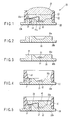
- FIG. 1 is a longitudinal sectional view showing a lens-equipped light-emitting diode device 10 according to a first embodiment of the invention.
- the lens-equipped light-emitting diode device 10 includes a lead frame 20, an outer peripheral unit 30, a sealing portion 40, and a lens unit 50.
- the lead frame 20 is a support member in which an electrode is formed.
- the outer peripheral unit 30 is formed on the lead frame 20.
- the sealing portion 40 is provided in the outer peripheral unit 30 and seals a light-emitting diode 22 and a bonding wire 23.
- the lens unit 50 is arranged in an upper portion of the sealing portion 40.
- Plural electrodes 21 are formed on the side of a surface 20a of the lead frame 20, and a light-emitting diode 22 is mounted on the electrode 21.
- a bonding wire 23 is connected to one of the electrodes of the light-emitting diode 22, and the bonding wire 23 is connected to the electrode 21.
- the number 20b designates a backside of the lead frame 20.
- a white color thermoplastic resin such as PPA, PC, and epoxy resin is used as a first resin forming the outer peripheral unit 30.
- a thermosetting resin or a UV curing resin, such as a transparent epoxy resin and transparent silicone, is used as a second resin forming the sealing portion 40.
- a fluorescent material for wavelength conversion is mixed to the resin.
- the thermosetting resin such as the transparent epoxy resin and the transparent silicone or the thermoplastic resin such as PMMA, PC, and COP is used as a third resin forming the lens unit 50.
- the lead frame 20 is prepared as shown in FIG. 2, and the light-emitting diode element is mounted on the lead frame with a die mounting material (not shown) as shown in FIG. 3. Then, these components are inserted in an injection molding die to form the outer peripheral unit 30 using a first white thermoplastic resin as shown in FIG. 4.
- wire bonding is performed between the electrode of the light-emitting diode element 22 and the electrode 21 of the lead frame 20, and the sealing portion 40 is formed around the light-emitting diode element 22 using a second sealing resin.
- the sealing portion 40 may be formed by the injection mold with the die or a potting method.
- molded components are inserted in the injection molding die different from those for molding the outer peripheral unit 30 and the sealing portion 40, and a lens unit 50 is integrally molded using a third transparent resin as shown in FIG. 6.
- a LIM method is adopted in the case where the thermosetting resin is used, and the injection molding method is adopted in the case where the thermoplastic resin is used.
- the molding of the lens unit 50 and the attachment of the lens unit 50 to the outer peripheral unit 30 can simultaneously be performed, a process of attaching a resin lens produced by another process to the outer peripheral unit and a process of adjusting an optical axis are not required, which allows cost to be reduced in an assembly process.
- a gap generated between the lens unit 50 and the outer peripheral unit 30 and a gap generated between the lens unit 50 and the sealing portion 40 can be prevented to improve the light extraction efficiency. Furthermore, attachment strength can be enhanced because the resins are fused at a boundary surface between the lens unit 50 and the sealing portion 40.
- the lens-equipped light-emitting diode device of the first embodiment is excellent in the light extraction efficiency and the reliability, and the production cost can be reduced.
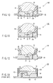
- FIG. 7 is a longitudinal sectional view showing a lens-equipped light-emitting diode device 10A according to a second embodiment of the invention.
- the same components as those of FIG. 1 are designated by the same numbers, and detailed description thereof will be omitted.
- a penetration portion 51 is provided in the lens unit 50, and the penetration portion 51 is latched in the lead frame 20 at a front-edge portion 52 of the penetration portion 51.
- the penetration portion 51 penetrates the lead frame 20 to the backside 20b where the light-emitting diode 22 is not mounted.
- the same effect as the lens-equipped light-emitting diode device 10 can also be obtained.
- the lens-equipped light-emitting diode device 10A further has the following effect.
- the resins forming the outer peripheral unit 30 and the lens unit 50 are different from each other, it is difficult to secure adhesive strength between the outer peripheral unit 30 and the lens unit 50. Therefore, in the integral molding with the lens unit 50, the penetration portion 51 is formed to prevent drop-out of the lens unit 50 in such a manner that the penetration portion 51 is filled with a transparent resin to the backside 20b of the lead frame 20. This enables the adhesive strength to be enhanced to improve the reliability.
- the resin having a large shrinkage ratio and linear thermal expansion coefficient is used as the third resin forming the lens unit 51, which allows the effect to be increased.
- the thermoplastic resin or the thermosetting resin can be used as the third resin.
- FIG. 8 is a longitudinal sectional view showing a lens-equipped light-emitting diode device 10B according to a third embodiment of the invention.
- the same components as those of FIG. 1 are designated by the same numbers, and detailed description thereof will be omitted.
- a penetration portion 53 is provided in the lens unit 50, and the penetration portion 53 is latched in the lead frame 20 at a front-edge portion 54 of the penetration portion 53.
- the penetration portion 53 penetrates the outer peripheral unit 30 and the lead frame 20 to the backside 20b where the light-emitting diode 22 is not mounted.
- the same effect as the lens-equipped light-emitting diode device 10A can also be obtained.
- FIG. 9 is a longitudinal sectional view showing a lens-equipped light-emitting diode device 10C according to a fourth embodiment of the invention.
- the same components as those of FIG. 1 are designated by the same numbers, and detailed description thereof will be omitted.
- a micro-rib 31 is provided in an upper edge portion of the outer peripheral unit 30.
- the same effect as the lens-equipped light-emitting diode device 10 can also be obtained, and only the micro-rib 31 is re-melted to weld the lens unit 50 by heat of the transparent resin when the lens unit 50 is molded. At this point, the welding strength can be enhanced by utilizing the resin having a higher melting point.
- the thermoplastic resin is used as the first resin and the third resin.
- FIG. 10 is a longitudinal sectional view showing a lens-equipped light-emitting diode device 10D according to a fifth embodiment of the invention.
- the same components as those of FIG. 1 are designated by the same numbers, and detailed description thereof will be omitted.
- a notch portion 24 is provided in the lead frame 20.
- a latch portion 55 is provided in the lens unit 50, and a front-edge portion 56 of the latch portion 55 is engaged with the notch portion 24.
- the latch portion 55 penetrates the lead frame 20, and is extended to the backside 20b where the light-emitting diode 22 is not mounted.
- the same effect as the lens-equipped light-emitting diode device 10A can also be obtained.
- FIG. 11 is a longitudinal sectional view showing a lens-equipped light-emitting diode device 10E according to a sixth embodiment of the invention.
- the same components as those of FIG. 1 are designated by the same numbers, and detailed description thereof will be omitted.
- the lens-equipped light-emitting diode device 10E can be applied to the case where the latch portion 55 is provided in a side face different from that of the lens-equipped light-emitting diode device 10D.
- the notch portion 24 is provided in the lead frame 20.
- the latch portion 55 is also provided in the lens unit 50, and the front-edge portion 56 of the latch portion 55 is engaged with the notch portion 24.
- the latch portion 55 is extended along the side face of the lead frame 20, and the latch portion 55 is extended to the backside 20b where the light-emitting diode 22 is not mounted.
- the same effect as the lens-equipped light-emitting diode device 10D can also be obtained.
- the latch portion 55 penetrate the lead frame 20.
- FIG. 12 is a longitudinal sectional view showing a lens-equipped light-emitting diode device 10F according to a seventh embodiment of the invention.
- the same components as those of FIG. 1 are designated by the same numbers, and detailed description thereof will be omitted.
- a through hole 32 is provided in the outer peripheral unit 30.
- a latch portion 57 is provided in the lens unit 50 while inserted into the through hole 32, and a front-edge portion 58 is engaged with the through hole 32.
- the notch portion may be provided in place of the through hole 32.
- the same effect as the lens-equipped light-emitting diode device 10A can also be obtained.
- the electrode of the light-emitting diode element 22 may be connected to the external electrode 21 not by the wire bonding but by the flip chip bonding.
- the light-emitting diode element 22 may be mounted after the outer peripheral unit 30 is formed in the lead frame 20 using the white resin.
- the lens integral molding can also be injection-molded not on the lead frame 20 but on a support member in which the electrode is formed, e.g., a glass epoxy substrate and a ceramic substrate.
Landscapes
- Engineering & Computer Science (AREA)
- Manufacturing & Machinery (AREA)
- Mechanical Engineering (AREA)
- Led Device Packages (AREA)
Applications Claiming Priority (1)
| Application Number | Priority Date | Filing Date | Title |
|---|---|---|---|
| JP2005373498A JP4965858B2 (ja) | 2005-12-26 | 2005-12-26 | レンズ付発光ダイオード装置 |
Publications (2)
| Publication Number | Publication Date |
|---|---|
| EP1801893A2 true EP1801893A2 (de) | 2007-06-27 |
| EP1801893A3 EP1801893A3 (de) | 2011-08-03 |
Family
ID=37888282
Family Applications (1)
| Application Number | Title | Priority Date | Filing Date |
|---|---|---|---|
| EP06026839A Withdrawn EP1801893A3 (de) | 2005-12-26 | 2006-12-22 | Mit einer Linse versehenen lichtemittierende Diodenvorrichtung und dessen Herstellungsverfahren |
Country Status (4)
| Country | Link |
|---|---|
| US (1) | US7378647B2 (de) |
| EP (1) | EP1801893A3 (de) |
| JP (1) | JP4965858B2 (de) |
| CN (1) | CN1992361B (de) |
Cited By (3)
| Publication number | Priority date | Publication date | Assignee | Title |
|---|---|---|---|---|
| WO2009072786A2 (en) | 2007-12-06 | 2009-06-11 | Seoul Semiconductor Co., Ltd. | Led package and method for fabricating the same |
| GB2466633A (en) * | 2008-12-12 | 2010-07-07 | Glory Science Co Ltd | Method of manufacturing a light emitting unit |
| EP2846368B1 (de) * | 2013-09-04 | 2019-04-24 | LG Innotek Co., Ltd. | Gehäuse für lichtemittierende Vorrichtung |
Families Citing this family (25)
| Publication number | Priority date | Publication date | Assignee | Title |
|---|---|---|---|---|
| US6697658B2 (en) | 2001-07-02 | 2004-02-24 | Masimo Corporation | Low power pulse oximeter |
| JP5328159B2 (ja) | 2005-03-01 | 2013-10-30 | セルカコア・ラボラトリーズ・インコーポレーテッド | 多波長センサ発光体 |
| US8044412B2 (en) | 2006-01-20 | 2011-10-25 | Taiwan Semiconductor Manufacturing Company, Ltd | Package for a light emitting element |
| JP2009094282A (ja) * | 2007-10-09 | 2009-04-30 | Cosmo Electronics Corp | ハイパワー発光ダイオード構造 |
| JP2009206370A (ja) * | 2008-02-28 | 2009-09-10 | Apic Yamada Corp | Ledパッケージ用基板、ledパッケージ用基板の製造方法、ledパッケージ用基板のモールド金型、ledパッケージ、及び、ledパッケージの製造方法 |
| US20100004518A1 (en) | 2008-07-03 | 2010-01-07 | Masimo Laboratories, Inc. | Heat sink for noninvasive medical sensor |
| US8630691B2 (en) | 2008-08-04 | 2014-01-14 | Cercacor Laboratories, Inc. | Multi-stream sensor front ends for noninvasive measurement of blood constituents |
| JP5368809B2 (ja) * | 2009-01-19 | 2013-12-18 | ローム株式会社 | Ledモジュールの製造方法およびledモジュール |
| CN101852384B (zh) * | 2009-03-31 | 2013-08-28 | 光宝科技股份有限公司 | 形成发光二极管的透镜结构的方法及其相关架构 |
| TWI485878B (zh) * | 2009-04-01 | 2015-05-21 | 光寶科技股份有限公司 | 形成發光二極體之透鏡結構之方法及其相關架構 |
| TW201041192A (en) * | 2009-05-11 | 2010-11-16 | Semi Photonics Co Ltd | LED device with a roughened light extraction structure and manufacturing methods thereof |
| KR101114197B1 (ko) * | 2010-08-09 | 2012-02-22 | 엘지이노텍 주식회사 | 발광 소자 및 이를 구비한 조명 시스템 |
| WO2012102107A1 (ja) * | 2011-01-28 | 2012-08-02 | 昭和電工株式会社 | 量子ドット蛍光体を含む組成物、量子ドット蛍光体分散樹脂成形体、量子ドット蛍光体を含む構造物、発光装置、電子機器、機械装置及び量子ドット蛍光体分散樹脂成形体の製造方法 |
| CA2842434A1 (en) | 2011-08-05 | 2013-02-14 | Gui Global Products, Ltd. | Apparatus for cleaning view screens and lenses and method for the use thereof |
| TW201415673A (zh) * | 2012-10-03 | 2014-04-16 | 隆達電子股份有限公司 | 發光裝置 |
| US20200137906A9 (en) | 2012-11-05 | 2020-04-30 | Gui Global Products, Ltd. | Devices and accessories employing a living hinge |
| KR101433261B1 (ko) | 2013-01-15 | 2014-08-27 | 루미마이크로 주식회사 | 발광소자 |
| CN103400927B (zh) * | 2013-07-25 | 2016-04-27 | 广东晶科电子股份有限公司 | 一种高可靠性led支架及其led器件 |
| JP2015050016A (ja) * | 2013-08-30 | 2015-03-16 | 東芝ライテック株式会社 | 発光モジュール及び照明装置 |
| JP6179555B2 (ja) * | 2015-06-01 | 2017-08-16 | 日亜化学工業株式会社 | 発光装置 |
| JP6110528B2 (ja) * | 2016-02-03 | 2017-04-05 | 京セラコネクタプロダクツ株式会社 | 半導体発光素子用ホルダ、及び、半導体発光素子モジュール |
| JP6680302B2 (ja) * | 2018-01-10 | 2020-04-15 | 日亜化学工業株式会社 | 発光装置 |
| KR20220129033A (ko) | 2020-01-13 | 2022-09-22 | 마시모 코오퍼레이션 | 생리학적 파라미터 모니터링 기능이 있는 웨어러블 디바이스 |
| JP7299537B2 (ja) * | 2020-03-18 | 2023-06-28 | 日亜化学工業株式会社 | 発光装置 |
| EP4370022A1 (de) | 2021-07-13 | 2024-05-22 | Masimo Corporation | Tragbare vorrichtung mit überwachung physiologischer parameter |
Family Cites Families (25)
| Publication number | Priority date | Publication date | Assignee | Title |
|---|---|---|---|---|
| JPS63318173A (ja) * | 1987-06-19 | 1988-12-27 | New Japan Radio Co Ltd | 光半導体装置の製造方法 |
| JPH03254162A (ja) * | 1990-03-02 | 1991-11-13 | Mitsui Petrochem Ind Ltd | 発光素子用キャップ、そのキャップを用いた発光素子、その製造方法及び装置 |
| IT1265106B1 (it) * | 1993-07-23 | 1996-10-30 | Solari Udine Spa | Sistema ottico per diodi emettitori di luce |
| JPH07307492A (ja) * | 1994-05-11 | 1995-11-21 | Mitsubishi Cable Ind Ltd | Led集合体モジュールおよびその作製方法 |
| JP3141373B2 (ja) * | 1996-01-18 | 2001-03-05 | 日亜化学工業株式会社 | 光電装置 |
| JP3492178B2 (ja) * | 1997-01-15 | 2004-02-03 | 株式会社東芝 | 半導体発光装置及びその製造方法 |
| US6274890B1 (en) * | 1997-01-15 | 2001-08-14 | Kabushiki Kaisha Toshiba | Semiconductor light emitting device and its manufacturing method |
| JP2000108144A (ja) * | 1998-10-06 | 2000-04-18 | Taiyo Ltd | 部品の製造方法 |
| JP2000156528A (ja) * | 1998-11-19 | 2000-06-06 | Sharp Corp | 発光素子 |
| JP3913435B2 (ja) * | 2000-02-29 | 2007-05-09 | 株式会社小糸製作所 | 車両用灯具の製造方法 |
| JP3614776B2 (ja) * | 2000-12-19 | 2005-01-26 | シャープ株式会社 | チップ部品型ledとその製造方法 |
| JP2002299699A (ja) * | 2001-03-30 | 2002-10-11 | Sumitomo Electric Ind Ltd | 発光装置およびその製造方法 |
| JP2004071908A (ja) * | 2002-08-07 | 2004-03-04 | Matsushita Electric Works Ltd | 発光装置 |
| US6682331B1 (en) * | 2002-09-20 | 2004-01-27 | Agilent Technologies, Inc. | Molding apparatus for molding light emitting diode lamps |
| JP2004265979A (ja) * | 2003-02-28 | 2004-09-24 | Noritsu Koki Co Ltd | 発光ダイオード光源ユニット |
| JP4599857B2 (ja) | 2003-04-24 | 2010-12-15 | 日亜化学工業株式会社 | 半導体装置及びその製造方法 |
| JP2005197369A (ja) * | 2004-01-05 | 2005-07-21 | Toshiba Corp | 光半導体装置 |
| JP2005223216A (ja) * | 2004-02-06 | 2005-08-18 | Matsushita Electric Ind Co Ltd | 発光光源、照明装置及び表示装置 |
| KR100585916B1 (ko) * | 2004-03-30 | 2006-06-01 | 서울반도체 주식회사 | 발광 다이오드 |
| US7280288B2 (en) * | 2004-06-04 | 2007-10-09 | Cree, Inc. | Composite optical lens with an integrated reflector |
| JP4146406B2 (ja) * | 2004-08-31 | 2008-09-10 | シャープ株式会社 | 発光素子および発光素子の製造方法 |
| EP1794808B1 (de) * | 2004-09-10 | 2017-08-09 | Seoul Semiconductor Co., Ltd. | Leuchtdiodenkapselung mit mehreren formharzen |
| JP2006261049A (ja) * | 2005-03-18 | 2006-09-28 | Koizumi Sangyo Corp | 多点光源ユニット |
| JP2006351816A (ja) * | 2005-06-16 | 2006-12-28 | Toshiaki Inoue | 砲弾型発光ダイオードレンズキャップ |
| JP2007080879A (ja) * | 2005-09-09 | 2007-03-29 | Matsushita Electric Works Ltd | Ledユニット |
-
2005
- 2005-12-26 JP JP2005373498A patent/JP4965858B2/ja not_active Expired - Fee Related
-
2006
- 2006-09-05 CN CN200610129054.3A patent/CN1992361B/zh not_active Expired - Fee Related
- 2006-12-20 US US11/613,503 patent/US7378647B2/en not_active Expired - Fee Related
- 2006-12-22 EP EP06026839A patent/EP1801893A3/de not_active Withdrawn
Cited By (5)
| Publication number | Priority date | Publication date | Assignee | Title |
|---|---|---|---|---|
| WO2009072786A2 (en) | 2007-12-06 | 2009-06-11 | Seoul Semiconductor Co., Ltd. | Led package and method for fabricating the same |
| US9698319B2 (en) | 2007-12-06 | 2017-07-04 | Seoul Semiconductor Co., Ltd. | LED package with lead terminals having protrusions of differing widths and method for fabricating the same |
| EP2215667B1 (de) * | 2007-12-06 | 2019-02-27 | Seoul Semiconductor Co., Ltd. | Herstellungsverfahren für ein led-bauelement |
| GB2466633A (en) * | 2008-12-12 | 2010-07-07 | Glory Science Co Ltd | Method of manufacturing a light emitting unit |
| EP2846368B1 (de) * | 2013-09-04 | 2019-04-24 | LG Innotek Co., Ltd. | Gehäuse für lichtemittierende Vorrichtung |
Also Published As
| Publication number | Publication date |
|---|---|
| JP2007180069A (ja) | 2007-07-12 |
| JP4965858B2 (ja) | 2012-07-04 |
| CN1992361A (zh) | 2007-07-04 |
| US7378647B2 (en) | 2008-05-27 |
| CN1992361B (zh) | 2010-05-12 |
| US20070145255A1 (en) | 2007-06-28 |
| EP1801893A3 (de) | 2011-08-03 |
Similar Documents
| Publication | Publication Date | Title |
|---|---|---|
| US7378647B2 (en) | Lens-equipped light-emitting diode device having an integrally molded lens unit being laminated on a sealing portion | |
| JP4945106B2 (ja) | 半導体発光装置 | |
| CN100382345C (zh) | 光半导体装置 | |
| CN101499429B (zh) | 注射成形用模具、半导体封装和半导体封装的制造方法 | |
| JP5720759B2 (ja) | 光半導体装置 | |
| KR101843402B1 (ko) | 표면 장착 가능한 광전자 소자 그리고 표면 장착 가능한 광전자 소자를 제조하기 위한 방법 | |
| US20060049422A1 (en) | Surface mount LED | |
| CN101361201B (zh) | 光元件的树脂密封成形方法 | |
| JP2010003743A (ja) | 発光装置 | |
| JP2011176347A (ja) | 反射レンズを備えたパワー発光ダイパッケージ | |
| TW201448290A (zh) | 發光裝置及其製造方法 | |
| JP2007311445A (ja) | 半導体発光装置及びその製造方法 | |
| JP2002368281A (ja) | 発光ダイオードの製造方法 | |
| KR20130114745A (ko) | 렌즈 부착 광반도체 장치 및 그 제조방법 | |
| KR20100115365A (ko) | 발광 장치 | |
| JP2012038999A (ja) | 発光デバイス及びその製造方法 | |
| US11929452B2 (en) | Method of manufacturing light-emitting device and method of manufacturing illumination device | |
| JP5180694B2 (ja) | Ledチップ実装用基板の製造方法、ledチップ実装用基板のモールド金型、ledチップ実装用基板、及び、led | |
| JP2007005378A (ja) | 発光装置、発光装置の製造方法および電子機器 | |
| JP2016213250A (ja) | パッケージ及びその製造方法、並びに発光装置 | |
| KR101945057B1 (ko) | 광학 반도체 장치용 베이스 및 그의 제조 방법, 및 광학 반도체 장치 | |
| JP2008140944A (ja) | 発光装置およびその製造方法 | |
| KR20140121507A (ko) | 플래시용 led 모듈 및 그 제조방법 | |
| JP4884074B2 (ja) | 半導体発光装置 | |
| JP2018157232A (ja) | パッケージ、発光装置及びそれらの製造方法 |
Legal Events
| Date | Code | Title | Description |
|---|---|---|---|
| PUAI | Public reference made under article 153(3) epc to a published international application that has entered the european phase |
Free format text: ORIGINAL CODE: 0009012 |
|
| 17P | Request for examination filed |
Effective date: 20061222 |
|
| AK | Designated contracting states |
Kind code of ref document: A2 Designated state(s): AT BE BG CH CY CZ DE DK EE ES FI FR GB GR HU IE IS IT LI LT LU LV MC NL PL PT RO SE SI SK TR |
|
| AX | Request for extension of the european patent |
Extension state: AL BA HR MK YU |
|
| PUAL | Search report despatched |
Free format text: ORIGINAL CODE: 0009013 |
|
| AK | Designated contracting states |
Kind code of ref document: A3 Designated state(s): AT BE BG CH CY CZ DE DK EE ES FI FR GB GR HU IE IS IT LI LT LU LV MC NL PL PT RO SE SI SK TR |
|
| AX | Request for extension of the european patent |
Extension state: AL BA HR MK RS |
|
| RIC1 | Information provided on ipc code assigned before grant |
Ipc: H01L 33/00 20100101AFI20110630BHEP |
|
| AKX | Designation fees paid |
Designated state(s): DE FR GB |
|
| STAA | Information on the status of an ep patent application or granted ep patent |
Free format text: STATUS: THE APPLICATION HAS BEEN WITHDRAWN |
|
| 18W | Application withdrawn |
Effective date: 20160111 |