EP1798778A2 - Integrierte Dünnfilm-Solarzelle und Verfahren zu ihrer Herstellung - Google Patents
Integrierte Dünnfilm-Solarzelle und Verfahren zu ihrer Herstellung Download PDFInfo
- Publication number
- EP1798778A2 EP1798778A2 EP06025934A EP06025934A EP1798778A2 EP 1798778 A2 EP1798778 A2 EP 1798778A2 EP 06025934 A EP06025934 A EP 06025934A EP 06025934 A EP06025934 A EP 06025934A EP 1798778 A2 EP1798778 A2 EP 1798778A2
- Authority
- EP
- European Patent Office
- Prior art keywords
- conductive material
- solar cell
- substrate
- transparent conductive
- forming
- Prior art date
- Legal status (The legal status is an assumption and is not a legal conclusion. Google has not performed a legal analysis and makes no representation as to the accuracy of the status listed.)
- Withdrawn
Links
- 239000010409 thin film Substances 0.000 title claims abstract description 72
- 238000004519 manufacturing process Methods 0.000 title claims abstract description 37
- 239000004020 conductor Substances 0.000 claims abstract description 320
- 239000000758 substrate Substances 0.000 claims abstract description 174
- 238000000034 method Methods 0.000 claims abstract description 132
- 238000000151 deposition Methods 0.000 claims abstract description 68
- 238000005530 etching Methods 0.000 claims abstract description 44
- 238000000059 patterning Methods 0.000 claims abstract description 42
- 229910052751 metal Inorganic materials 0.000 claims description 70
- 239000002184 metal Substances 0.000 claims description 70
- 239000010408 film Substances 0.000 claims description 26
- 229920002120 photoresistant polymer Polymers 0.000 claims description 16
- 239000007769 metal material Substances 0.000 claims description 15
- 229920000642 polymer Polymers 0.000 claims description 14
- 238000007639 printing Methods 0.000 claims description 13
- 239000011248 coating agent Substances 0.000 claims description 6
- 238000000576 coating method Methods 0.000 claims description 6
- 238000004049 embossing Methods 0.000 claims description 2
- 239000004065 semiconductor Substances 0.000 abstract description 33
- 239000010410 layer Substances 0.000 description 91
- 230000008021 deposition Effects 0.000 description 41
- XOLBLPGZBRYERU-UHFFFAOYSA-N tin dioxide Chemical compound O=[Sn]=O XOLBLPGZBRYERU-UHFFFAOYSA-N 0.000 description 36
- 238000010586 diagram Methods 0.000 description 33
- 229910021417 amorphous silicon Inorganic materials 0.000 description 32
- 229910052782 aluminium Inorganic materials 0.000 description 24
- XAGFODPZIPBFFR-UHFFFAOYSA-N aluminium Chemical compound [Al] XAGFODPZIPBFFR-UHFFFAOYSA-N 0.000 description 24
- PCHJSUWPFVWCPO-UHFFFAOYSA-N gold Chemical compound [Au] PCHJSUWPFVWCPO-UHFFFAOYSA-N 0.000 description 16
- XUIMIQQOPSSXEZ-UHFFFAOYSA-N Silicon Chemical compound [Si] XUIMIQQOPSSXEZ-UHFFFAOYSA-N 0.000 description 15
- 229910000577 Silicon-germanium Inorganic materials 0.000 description 15
- 229910052710 silicon Inorganic materials 0.000 description 15
- 239000010703 silicon Substances 0.000 description 15
- XLOMVQKBTHCTTD-UHFFFAOYSA-N Zinc monoxide Chemical compound [Zn]=O XLOMVQKBTHCTTD-UHFFFAOYSA-N 0.000 description 14
- AMGQUBHHOARCQH-UHFFFAOYSA-N indium;oxotin Chemical compound [In].[Sn]=O AMGQUBHHOARCQH-UHFFFAOYSA-N 0.000 description 12
- 238000003754 machining Methods 0.000 description 12
- 229910001887 tin oxide Inorganic materials 0.000 description 12
- 238000009413 insulation Methods 0.000 description 11
- 239000000203 mixture Substances 0.000 description 8
- 238000002310 reflectometry Methods 0.000 description 8
- 239000000126 substance Substances 0.000 description 8
- 238000009834 vaporization Methods 0.000 description 8
- 230000008016 vaporization Effects 0.000 description 8
- 238000010894 electron beam technology Methods 0.000 description 6
- KTSFMFGEAAANTF-UHFFFAOYSA-N [Cu].[Se].[Se].[In] Chemical compound [Cu].[Se].[Se].[In] KTSFMFGEAAANTF-UHFFFAOYSA-N 0.000 description 5
- 150000001875 compounds Chemical class 0.000 description 5
- 238000005520 cutting process Methods 0.000 description 4
- 238000005516 engineering process Methods 0.000 description 4
- LEVVHYCKPQWKOP-UHFFFAOYSA-N [Si].[Ge] Chemical compound [Si].[Ge] LEVVHYCKPQWKOP-UHFFFAOYSA-N 0.000 description 3
- 238000005137 deposition process Methods 0.000 description 3
- 238000000313 electron-beam-induced deposition Methods 0.000 description 3
- 229910021432 inorganic complex Inorganic materials 0.000 description 3
- 238000000206 photolithography Methods 0.000 description 3
- 229910021425 protocrystalline silicon Inorganic materials 0.000 description 3
- 239000002994 raw material Substances 0.000 description 3
- 238000002207 thermal evaporation Methods 0.000 description 3
- MARUHZGHZWCEQU-UHFFFAOYSA-N 5-phenyl-2h-tetrazole Chemical compound C1=CC=CC=C1C1=NNN=N1 MARUHZGHZWCEQU-UHFFFAOYSA-N 0.000 description 2
- 238000006243 chemical reaction Methods 0.000 description 2
- 239000000356 contaminant Substances 0.000 description 2
- 229910021419 crystalline silicon Inorganic materials 0.000 description 2
- 230000006866 deterioration Effects 0.000 description 2
- 230000000694 effects Effects 0.000 description 2
- 238000001020 plasma etching Methods 0.000 description 2
- 229910021420 polycrystalline silicon Inorganic materials 0.000 description 2
- 239000000523 sample Substances 0.000 description 2
- JBRZTFJDHDCESZ-UHFFFAOYSA-N AsGa Chemical compound [As]#[Ga] JBRZTFJDHDCESZ-UHFFFAOYSA-N 0.000 description 1
- GPXJNWSHGFTCBW-UHFFFAOYSA-N Indium phosphide Chemical compound [In]#P GPXJNWSHGFTCBW-UHFFFAOYSA-N 0.000 description 1
- ZOKXTWBITQBERF-UHFFFAOYSA-N Molybdenum Chemical compound [Mo] ZOKXTWBITQBERF-UHFFFAOYSA-N 0.000 description 1
- 238000007796 conventional method Methods 0.000 description 1
- 230000002542 deteriorative effect Effects 0.000 description 1
- 238000011161 development Methods 0.000 description 1
- 238000001312 dry etching Methods 0.000 description 1
- 230000005611 electricity Effects 0.000 description 1
- 239000011521 glass Substances 0.000 description 1
- 239000012212 insulator Substances 0.000 description 1
- 239000000463 material Substances 0.000 description 1
- 238000012986 modification Methods 0.000 description 1
- 230000004048 modification Effects 0.000 description 1
- 229910052750 molybdenum Inorganic materials 0.000 description 1
- 239000011733 molybdenum Substances 0.000 description 1
- 229920003023 plastic Polymers 0.000 description 1
- 238000012545 processing Methods 0.000 description 1
- 239000011241 protective layer Substances 0.000 description 1
- 239000011347 resin Substances 0.000 description 1
- 229920005989 resin Polymers 0.000 description 1
- 238000007650 screen-printing Methods 0.000 description 1
- 238000004544 sputter deposition Methods 0.000 description 1
- 239000011787 zinc oxide Substances 0.000 description 1
Images


Classifications
-
- H—ELECTRICITY
- H01—ELECTRIC ELEMENTS
- H01L—SEMICONDUCTOR DEVICES NOT COVERED BY CLASS H10
- H01L31/00—Semiconductor devices sensitive to infrared radiation, light, electromagnetic radiation of shorter wavelength or corpuscular radiation and specially adapted either for the conversion of the energy of such radiation into electrical energy or for the control of electrical energy by such radiation; Processes or apparatus specially adapted for the manufacture or treatment thereof or of parts thereof; Details thereof
- H01L31/18—Processes or apparatus specially adapted for the manufacture or treatment of these devices or of parts thereof
- H01L31/1804—Processes or apparatus specially adapted for the manufacture or treatment of these devices or of parts thereof comprising only elements of Group IV of the Periodic Table
-
- H—ELECTRICITY
- H01—ELECTRIC ELEMENTS
- H01L—SEMICONDUCTOR DEVICES NOT COVERED BY CLASS H10
- H01L31/00—Semiconductor devices sensitive to infrared radiation, light, electromagnetic radiation of shorter wavelength or corpuscular radiation and specially adapted either for the conversion of the energy of such radiation into electrical energy or for the control of electrical energy by such radiation; Processes or apparatus specially adapted for the manufacture or treatment thereof or of parts thereof; Details thereof
- H01L31/04—Semiconductor devices sensitive to infrared radiation, light, electromagnetic radiation of shorter wavelength or corpuscular radiation and specially adapted either for the conversion of the energy of such radiation into electrical energy or for the control of electrical energy by such radiation; Processes or apparatus specially adapted for the manufacture or treatment thereof or of parts thereof; Details thereof adapted as photovoltaic [PV] conversion devices
- H01L31/042—PV modules or arrays of single PV cells
- H01L31/0445—PV modules or arrays of single PV cells including thin film solar cells, e.g. single thin film a-Si, CIS or CdTe solar cells
- H01L31/046—PV modules composed of a plurality of thin film solar cells deposited on the same substrate
- H01L31/0463—PV modules composed of a plurality of thin film solar cells deposited on the same substrate characterised by special patterning methods to connect the PV cells in a module, e.g. laser cutting of the conductive or active layers
-
- H—ELECTRICITY
- H01—ELECTRIC ELEMENTS
- H01L—SEMICONDUCTOR DEVICES NOT COVERED BY CLASS H10
- H01L31/00—Semiconductor devices sensitive to infrared radiation, light, electromagnetic radiation of shorter wavelength or corpuscular radiation and specially adapted either for the conversion of the energy of such radiation into electrical energy or for the control of electrical energy by such radiation; Processes or apparatus specially adapted for the manufacture or treatment thereof or of parts thereof; Details thereof
- H01L31/18—Processes or apparatus specially adapted for the manufacture or treatment of these devices or of parts thereof
-
- H—ELECTRICITY
- H01—ELECTRIC ELEMENTS
- H01L—SEMICONDUCTOR DEVICES NOT COVERED BY CLASS H10
- H01L31/00—Semiconductor devices sensitive to infrared radiation, light, electromagnetic radiation of shorter wavelength or corpuscular radiation and specially adapted either for the conversion of the energy of such radiation into electrical energy or for the control of electrical energy by such radiation; Processes or apparatus specially adapted for the manufacture or treatment thereof or of parts thereof; Details thereof
- H01L31/02—Details
- H01L31/0224—Electrodes
- H01L31/022466—Electrodes made of transparent conductive layers, e.g. TCO, ITO layers
-
- H—ELECTRICITY
- H01—ELECTRIC ELEMENTS
- H01L—SEMICONDUCTOR DEVICES NOT COVERED BY CLASS H10
- H01L31/00—Semiconductor devices sensitive to infrared radiation, light, electromagnetic radiation of shorter wavelength or corpuscular radiation and specially adapted either for the conversion of the energy of such radiation into electrical energy or for the control of electrical energy by such radiation; Processes or apparatus specially adapted for the manufacture or treatment thereof or of parts thereof; Details thereof
- H01L31/18—Processes or apparatus specially adapted for the manufacture or treatment of these devices or of parts thereof
- H01L31/1884—Manufacture of transparent electrodes, e.g. TCO, ITO
-
- Y—GENERAL TAGGING OF NEW TECHNOLOGICAL DEVELOPMENTS; GENERAL TAGGING OF CROSS-SECTIONAL TECHNOLOGIES SPANNING OVER SEVERAL SECTIONS OF THE IPC; TECHNICAL SUBJECTS COVERED BY FORMER USPC CROSS-REFERENCE ART COLLECTIONS [XRACs] AND DIGESTS
- Y02—TECHNOLOGIES OR APPLICATIONS FOR MITIGATION OR ADAPTATION AGAINST CLIMATE CHANGE
- Y02E—REDUCTION OF GREENHOUSE GAS [GHG] EMISSIONS, RELATED TO ENERGY GENERATION, TRANSMISSION OR DISTRIBUTION
- Y02E10/00—Energy generation through renewable energy sources
- Y02E10/50—Photovoltaic [PV] energy
- Y02E10/547—Monocrystalline silicon PV cells
-
- Y—GENERAL TAGGING OF NEW TECHNOLOGICAL DEVELOPMENTS; GENERAL TAGGING OF CROSS-SECTIONAL TECHNOLOGIES SPANNING OVER SEVERAL SECTIONS OF THE IPC; TECHNICAL SUBJECTS COVERED BY FORMER USPC CROSS-REFERENCE ART COLLECTIONS [XRACs] AND DIGESTS
- Y02—TECHNOLOGIES OR APPLICATIONS FOR MITIGATION OR ADAPTATION AGAINST CLIMATE CHANGE
- Y02P—CLIMATE CHANGE MITIGATION TECHNOLOGIES IN THE PRODUCTION OR PROCESSING OF GOODS
- Y02P70/00—Climate change mitigation technologies in the production process for final industrial or consumer products
- Y02P70/50—Manufacturing or production processes characterised by the final manufactured product
Definitions
- the present invention relates to an integrated thin-film solar cell, and more particularly, to an integrated thin-film solar cell minimizing its loss incurred in a manufacture process and achieved even by a cheap process, and a method of manufacturing the same.
- Solar cell refers to a semiconductor device for directly converting solar energy into electricity.
- the solar cell can be mainly classified into a silicon-based solar cell, a compound-based solar cell, and an organic solar cell depending on its use material.
- the silicon-based solar cell is in detail classified into a single crystalline silicon solar cell, a polycrystalline silicon solar cell, and an amorphous silicon solar cell depending on a semiconductor phase.
- the solar cell is classified into a bulk (substrate) solar cell and a thin film solar cell depending on a semiconductor thickness.
- a semiconductor layer has a thickness of to several ⁇ m to several tens of ⁇ m.
- the single crystalline and polycrystalline silicon solar cells belong to the bulk solar cell.
- the amorphous silicon solar cell belongs to the thin film solar cell.
- the compound-based solar cell is classified into the bulk solar cell based on gallium arsenide (GaAs) and indium phosphide (InP) of groups III-V, and the thin film solar cell based on cadmium telluride (CdTe) of groups II-VI and copper indium diselenide (CIS) (CuInSe 2 ) of groups I-III-VI.
- the organic solar cell is mainly classified into an organic molecular solar cell and an organic/inorganic complex solar cell. In addition, there is a dye-sensitized solar cell. They all belong to the thin film solar cell.
- the bulk silicon solar cell having a high-energy conversion efficiency and a cheap manufacturing cost is being popularly utilized for ground power.
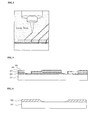
- FIG. 1 is a diagram illustrating a structure of a conventional integrated thin-film solar cell.
- FIG. 2 is a diagram illustrating an example of a laser patterning process for machining a transparent electrode, a solar cell (semiconductor) layer, a metal back electrode in a conventional integrated thin-film solar cell.
- a conventional integrated thin-film solar cell 1 is of a structure in which a plurality of unit cells 20 are connected in series and integrated on a glass substrate or transparent plastic substrate 10 (hereinafter, referred to as "transparent substrate").
- the integrated thin-film solar cell includes a transparent electrode 22 mutually cut (insulated), and formed in a band shape on the transparent substrate 10 that is an insulator; a unit solar cell (semiconductor) layer 24 covering the transparent electrode 22 and formed in a band shape; and a metal back electrode layer 26 covering the solar cell layer 24 and formed in a band shape.
- the integrated thin-film solar cell is of a structure in which the plurality of cut (insulated) unit cells 20 connect in series with each other.
- the metal back electrode is covered with a back protective layer 30 formed of resin for preventing electrical short-circuiting of the solar cell and protecting the solar cell.
- a laser patterning method In general, a laser patterning method, a chemical vaporization machining (CVM) method, a metal probe-based mechanical scribing method are being used to manufacture the integrated thin-film solar cell 1.
- CVM chemical vaporization machining
- the laser patterning method refers to a technology for etching the transparent electrode 22, the solar cell (semiconductor) layer 24, and the metal back electrode layer 26, mainly using YAG laser beam. A detailed usage method will be described as follows.
- the transparent electrode 22 is formed on the transparent substrate 10, and is etched using laser beam under the atmosphere.
- the solar cell (semiconductor) layer 24 is formed and is cut (insulated) using the laser beam under the atmosphere.
- the metal back electrode layer 26 is formed and is etched using the laser patterning process under the atmosphere, thereby electrically connecting the solar cells in series and forming the integrated solar cell.
- the transparent electrode 22 is formed on an entire upper surface of the transparent substrate 10. After that, the transparent electrode 22 is cut in the laser patterning method, and is cut (insulated) in the band shape having a predetermined width. Then, the cut transparent electrode 22 has a width of 50 ⁇ m to several 100 ⁇ m in general.
- the metal back electrode layer 26 is formed under the vacuum by a sputtering method and is again laser-patterned under the atmosphere, thereby manufacturing the integrated solar cell.
- This process can cause process discontinuity and contaminant drawbacks as described above.
- An ineffective area (cut width) between the unit cells 20 of the solar cell increases through a total of three-times laser patterning including two times of laser patterning for cutting the transparent electrode 22 and the solar cell (semiconductor) layer 24, and one time of laser patterning for cutting the metal back electrode layer 26 and concurrently electrically connecting the solar cells in series.
- a loss of an effective area of the solar cell increases.
- a laser patterning equipment is expensive, and a precision position control system is required for patterning at an accurate position, thereby increasing a manufacturing cost.
- the chemical vaporization machining method refers to a technology for simultaneously cutting the solar cell (semiconductor) layer into the plurality of unit cells having a uniform width, by locally generating atmospheric pressure plasma around line electrodes that have diameters of tens of ⁇ m and are arranged in a grid form in proximity to an upper portion of a substrate, using SF 6 /He gas.
- the chemical vaporization machining method has a feature of short process time, excellent film selectivity, and less film damage compared with the laser patterning method.
- the chemical vaporization machining method has an advantage of preventing a performance of the solar cell from being deteriorated by the exposure of the substrate to the atmosphere because etching is performed under the vacuum unlike the laser patterning method, and reducing the manufacturing cost compared with the laser patterning method.
- the precision position control system capable of accurately controlling a position within a vacuum device is needed because the etching should be performed in an accurate position adaptively to the patterned transparent electrode. This is of very difficult matter when the solar cell is manufactured using a large-scale substrate.
- a gap obtained by the etching is about 200 ⁇ m to the minimum, and is greater than an insulation gap obtained using the laser patterning method.
- Another etching method is the mechanical scribing method.
- This method makes it possible to perform collective scribing, by a plurality of metal probes, correspondingly to the number of necessary unit cells, and is greater in extensibility and adaptability to high-speed processing than the laser patterning method.
- the mechanical scribing method refers to an etching method in which device and operation costs are most cheap compared with the above two methods.
- a CdS/CIS layer is being popularly used to manufacture the CIS solar cell because it is softer than molybdenum (Mo), thereby facilitating scribing based on the scribing method.
- the conventional mechanical scribing method has a drawback that it needs the laser patterning equipment for etching a back electrode (Mo) and a front electrode (ZnO), and the precision position control device for accurately controlling the position because it is limitedly used only for the solar cell (semiconductor) layer.
- the present invention is to provide an integrated thin-film solar cell for reducing an insulation gap between unit elements reduces, thereby increasing an effective area of the solar cell, performing all processes under vacuum after forming a transparent electrode, and electrically connecting the unit elements of the solar cell in series by a simple process, thereby achieving its unit cell type.
- the present invention is to provide a method of manufacturing an integrated thin-film solar cell, for preventing deterioration of a performance of a unit cell, and reducing a manufacturing cost.
- the present invention is to provide a method of manufacturing an integrated thin-film solar cell, for acquiring a desired high voltage from one solar cell even while performance deterioration is as little as disregardful.
- a method of manufacturing an integrated thin-film solar cell comprises forming and patterning a first conductive material to be adjacently spaced a predetermined distance apart from each other on a substrate; forming a solar cell layer on the resultant substrate; obliquely depositing a second conductive material on the solar cell layer; etching the solar cell layer using the second conductive material as a mask; and obliquely depositing a third conductive material on the resultant substrate, and electrically connecting the first conductive material with the second conductive material adjacent to the first conductive material.
- the first to third conductive material may be a transparent conductive material or a metallic material.
- the transparent conductive material may be any one or more selected from the group consisting of zinc oxide (ZnO), tin oxide (SnO 2 ), and Indium Tin Oxide (ITO).
- ZnO zinc oxide
- SnO 2 tin oxide
- ITO Indium Tin Oxide
- the depositing of the second transparent conductive material may further comprise forming and patterning a metal electrode to be spaced a predetermined distance apart from each other.
- the forming of the conductive material further comprise thinly forming the first conductive material on the substrate; coating and forming a pattern of photoresist or polymer band to be spaced a predetermined distance apart on the first conductive material by a printing method; etching the first conductive material using the coated photoresist or polymer pattern as a mask; and removing the photoresist or polymer pattern.
- the conductive material is etched in an isotropic etching method to have a curved slant section as an etching section.
- the conductive material is mesa etched to have a slant section.
- the conductive material is etched in an anisotropic etching method so that etching is performed in a vertical direction of the substrate.
- the solar cell layer is etched in a vertical direction.
- the solar cell layer is obliquely etched in a slant direction.
- the substrate is a substrate with an insulating film formed on a conductive substrate, or an insulating substrate.
- an integrated thin-film solar cell whose unit elements electrically connect in series by the above solar cell manufacturing method.
- a method of manufacturing an integrated thin-film solar cell comprises forming and patterning a first conductive material to be adjacently spaced a predetermined distance apart from each other on a substrate; obliquely depositing a second conductive material on the resultant substrate; forming a solar cell layer on the resultant substrate; obliquely depositing a third conductive material on the solar cell layer; etching the solar cell layer using the third conductive material as a mask; and obliquely depositing a fourth conductive material on the resultant substrate, and electrically connecting the second conductive material with the third conductive material adjacent to the second conductive material.
- the first and second conductive materials may be transparent conductive materials or metallic materials.
- the first to fourth conductive materials are transparent conductive materials or metallic materials.
- the depositing of the second transparent conductive material further comprises: forming and patterning a metal electrode to be spaced a predetermined distance apart from each other.
- the substrate is a substrate with an insulating film formed on a conductive substrate, or an insulating substrate.
- an integrated thin-film solar cell whose unit elements electrically connect in series by the above solar cell manufacturing method.
- a method of manufacturing an integrated thin-film solar cell comprises obliquely depositing a first conductive material on a substrate on which prominence and depression are provided and spaced a predetermined distance apart from each other; forming a solar cell layer on the resultant substrate; obliquely depositing a second conductive material on the solar cell layer; etching the solar cell layer using the second conductive material as a mask; and obliquely depositing a third conductive material on the resultant substrate, and electrically connecting the first conductive material with the second conductive material.
- the first to third conductive materials are a transparent conductive material or a metallic material.
- the depositing of the second transparent conductive material further comprises: forming and patterning a metal electrode to be spaced a predetermined distance apart from each other.
- the substrate is a substrate with an insulating film formed on a conductive substrate, or an insulating substrate.
- an integrated thin-film solar cell whose unit elements electrically connect in series by the above solar cell manufacturing method.
- FIG. 1 is a diagram illustrating a structure of a conventional integrated thin-film solar cell
- FIG. 2 is a diagram illustrating an example of a laser patterning process for machining a transparent electrode, a solar cell (semiconductor) layer, a metal back electrode in a conventional integrated thin-film solar cell;
- FIG. 3 is a cross sectional diagram illustrating a structure of an integrated thin-film solar cell formed by two slant depositions on an insulating substrate according to an exemplary embodiment of the present invention
- FIG. 4 is a cross sectional view illustrating a substrate on which a patterned conductive material is formed according to the present invention
- FIG. 5 is a sequential diagram illustrating a printing method for patterning the conductive material of FIG. 4;
- FIGS. 6A and 6B illustrate patterned conductive materials according another exemplary embodiment of the present invention
- FIG. 7 is a cross sectional diagram illustrating a state where a solar cell layer is formed according to the present invention.
- FIG. 8 is a cross sectional diagram illustrating a state where a first transparent conductive material is formed according to the present invention.
- FIGS. 9A and 9B are cross sectional diagrams illustrating vertical etching states with a first transparent conductive material used as a mask according to the present invention.
- FIG. 9C is a cross sectional diagram illustrating a slant etching state with a first transparent conductive material used as a mask according to the present invention.
- FIGS. 10A and 10B are cross sectional diagrams illustrating states where second transparent conductive materials are formed according to the present invention.
- FIG. 11 is a cross sectional diagram illustrating a structure and a forming process of an integrated thin-film solar cell formed by two slant depositions on a conductive substrate according to another exemplary embodiment of the present invention
- FIG. 12 is a cross sectional diagram illustrating a structure and a forming process of an integrated thin-film solar cell formed by three slant depositions on an insulating substrate according to a further another exemplary embodiment of the present invention
- FIG. 13 is a cross sectional diagram illustrating a structure and a forming process of an integrated thin-film solar cell formed by three slant depositions on a conductive substrate according to a still another exemplary embodiment of the present invention
- FIG. 14 is a cross sectional diagram illustrating a structure and a forming process of an integrated thin-film solar cell formed by three slant depositions on an insulating substrate with prominence and depression according to a yet another exemplary embodiment of the present invention.
- FIG. 15 is a cross sectional diagram illustrating a structure and a forming process of an integrated thin-film solar cell formed by three slant depositions on a conductive substrate with prominence and depression according to a yet another exemplary embodiment of the present invention.
- a substrate refers to a substrate with an insulating film formed on a conductive substrate, or an insulating substrate.
- a description will be made for two cases where a substrate has a conductive property and an insulating property.
- the substrate comprises the substrate with the insulating film formed on the conductive substrate, and the insulating substrate. This is to employ the insulating film because the conductive substrate electrically connects with other conductive materials.
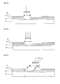
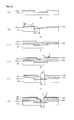
- FIG. 3 is a cross sectional diagram illustrating a structure of an integrated thin-film solar cell formed by two slant depositions on an insulating substrate 101 according to an exemplary embodiment of the present invention.
- the integrated thin-film solar cell according to the present invention is of a structure where a conductive material 102 having a slant section, a solar cell (semiconductor) layer 103, a first transparent conductive material 104, and a second transparent conductive material 105 are sequentially layered on the insulating substrate 101.
- the conductive material 102 is patterned to have an insulating gap for insulation from left/right adjacent conductive materials 102.
- the solar cell (semiconductor) layer and the first transparent conductive material 104 are deposited on the patterned conductive material 102.
- the second transparent conductive material 105 is positioned on the first transparent conductive material 104.
- the second transparent conductive material 105 is of a structure in which it gets in contact with and electrically connects in series with the adjacent conductive material 102 of one direction.
- the patterned conductive material 102 can have a slant section with a predetermined slope at its side portion. But, this is not intended to limit the scope of the present invention and thus, the patterned conductive material 102 can have a curved slant section or a section vertical with the substrate 101.
- a method of manufacturing the integrated thin-film solar cell will be described in sequence as follows.
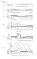
- FIGS. 4 to 10 are cross sectional diagrams sequentially illustrating a method of manufacturing the integrated solar cell according to the present invention.
- FIG. 4 is a cross sectional diagram illustrating the insulating substrate 101 on which the patterned conductive material 102 is formed according to the present invention.
- the patterned conductive material 102 is formed on the insulating substrate 101 in a first process of the manufacturing method of the integrated thin-film solar cell according to the present invention.
- the insulating substrate 101 is a transparent substrate or a non-transparent substrate.
- the conductive material 102 is a transparent conductive material that is any one or more selected from the group consisting of zinc oxide (ZnO), tin oxide (SnO 2 ), and Indium Tin Oxide (ITO), a single metal with a high reflectivity such as aluminum (Al), argentums (Ag), and aurum (Au), a multi metal being a mixture of aluminum (Al)/argentums (Ag), or a metallic material that is any one or more selected from the group consisting of argentums (Ag), aluminum (Al), and aurum (Au).
- ZnO zinc oxide
- SnO 2 tin oxide
- ITO Indium Tin Oxide
- a single metal with a high reflectivity such as aluminum (Al), argentums (Ag), and aurum (Au)
- a multi metal being a mixture of aluminum (Al)/argentums (Ag)
- the patterned conductive material 102 is possible for all cases where surface prominence and depression is provided or not.
- the conductive material 102 is thinly formed on the substrate 101, photoresist (PR) or polymer 102a is coated on the conductive material 102 by a printing method, and the photoresist or polymer 102a is coated so that the conductive material 102 is mutually spaced a predetermined distance apart by controlling a degree of viscosity of the printed photoresist or polymer 102a.
- the conductive material 102 is etched using the photoresist or polymer 102a as a mask. After that, the photoresist or polymer 102a is removed.
- the printing method refers to a screen printing method for coating and patterning a photoresist or polymer thin film by the simplest printing device and a simple and convenient cheap process, or a gravure press method for forming a fine pitch pattern.
- An anisotropic or isotropic etching method is used for etching the conductive material 102.
- the conductive material 102 can be patterned to have curved and slant surfaces at both sides and a width getting greater as it goes to a lower side as shown in FIG. 4.
- the conductive material 102 can be patterned to have the section vertical with the substrate 101, or the slant section with a predetermined slope as shown in FIGS. 6A and 6B.
- each printing method is used for etching the conductive material 102 as above, high-density pattern printing is possible, a thin film has an excellent homogeneity, a process is relatively simpler, and an expensive equipment for laser patterning is not needed unlike a conventional method. Thus, a manufacturing cost can reduce.
- the photoresist using a photolithography, instead of coating the polymer using the printing method.
- the photolithography is based on a principle in which the photoresist leads to a chemical reaction and varies its property when receiving light.
- a conductive material film can be directly coated on the substrate without using a photoresist or polymer pattern based on the printing method or the photolithography.
- the printing method makes it possible to directly form and pattern the conductive material film in a band shape in a low temperature process without the etching process using the mask.
- a transparent electrode refers to a conductive material.
- the solar cell layer 103 is formed on the above patterned conductive material 102 in compliance with a surface shape of the substrate 101.
- the solar cell can be any one or more of a silicon-based solar cell, a compound-based solar cell, an organic solar cell, a dry dye-sensitized solar cell, and an organic/inorganic complex solar cell.
- the silicon-based solar cell is any one of an amorphous silicon (a-Si:H) single junction solar cell, an a-Si:H/a-Si:H or a-Si:H/a-Si:H/a-Si:H multi-junction solar cell, an amorphous silicon-germanium (a-SiGe:H) single junction solar cell, an a-Si:H/a-SiGe:H double junction solar cell, an a-Si:H/a-SiGe:H/a-SiGe:H triple junction solar cell, an amorphous silicon/microcrystalline (polycrystalline) silicon double junction solar cell, and a protocrystalline silicon solar cell.
- a-Si:H amorphous silicon
- a-Si:H a-Si:H/a-Si:H or a-Si:H/a-Si:H/a-Si:H multi-junction solar cell
- FIG. 8 is a cross sectional diagram illustrating a state where the first transparent conductive material 104 is formed according to the present invention.
- the first transparent conductive material 104 is obliquely deposited and formed on the above formed solar cell layer 103 using a deposition method such as electron beam or thermal deposition.
- the first transparent conductive material 104 is a transparent conductive material, and is at least one selected from the group consisting of zinc oxide (ZnO), tin oxide (SnO 2 ), and Indium Tin Oxide (ITO).
- ZnO zinc oxide
- SnO 2 tin oxide
- ITO Indium Tin Oxide
- the first transparent conductive material 104 when the first transparent conductive material 104 is deposited on a slant with a first angle ( ⁇ 1 ) using an electron beam or thermal depositor, it is thinly deposited on the solar cell layer 103 excluding a portion (1a) comprising the slant surface, owing to deposition straightness (2a).
- the portion (1a) comprising the slant surface represents a region for etching implemented in the following step.
- FIGS. 9A and 9B are cross sectional diagrams illustrating vertical etching states with the first transparent conductive material 104 used as a mask according to the present invention. Three etching methods can be used depending on a section shape of the conductive material 102.
- the solar cell layer 103 is vertically etched using the deposited first transparent conductive material 104 of FIG. 7 as the mask. It is desirable to use a dry etching process such as Reactive Ion Etching (RIE).
- RIE Reactive Ion Etching
- the solar cell layer 103 is etched on a slant with a predetermined angle ( ⁇ 2 ) with respect to the substrate 101, using the deposited first transparent conductive material 104 of FIG. 7 as the mask.
- Non-described symbols 1b and 1c denote regions in which the first transparent conductive material 104 is not deposited over the conductive material 102' or 102" having the slant section or the vertical section.
- the region represents a region for etching implemented in the following step.
- This method can make it possible to minutely etch the solar cell layer 103 without needing a specific mask, thereby realizing the insulation gap of several ⁇ m to several tens of ⁇ m between the unit elements. This can reduce by more than tens of times to hundreds of times compared with conventional plasma-based chemical vaporization machining method and laser beam-based laser patterning method, thereby maximizing an effective area of the solar cell.
- FIG. 10A illustrates a process of forming the second transparent conductive material 105 on the first transparent conductive material 104 of FIG. 9A.
- FIG. 10B illustrates a process of forming the second transparent conductive material 105 on the first transparent conductive material 104 of FIG. 9C.
- a process of forming the second transparent conductive material 105 on the first transparent conductive material 104 of FIG. 9B is the same as that of FIG. 10A and thus, its description will be omitted.
- the second transparent conductive material 105 is formed using the same deposition process as the first transparent conductive material 104 in a state where a predetermined insulating gap between unit elements is provided in a previous etching process.
- the second transparent conductive materials 105 are deposited on a slant with predetermined angle ( ⁇ 3 and ⁇ 4 ) using an electron beam or thermal depositor, it is thinly deposited on the first transparent conductive material 104 excluding portions (1d) of the slant surfaces, owing to deposition straightness (2b and 2c).
- the second transparent conductive material 105 is a transparent conductive material, and is at least one selected from the group consisting of zinc oxide (ZnO), tin oxide (SnO 2 ), and Indium Tin Oxide (ITO).
- ZnO zinc oxide
- SnO 2 tin oxide
- ITO Indium Tin Oxide
- the conductive material 102 of a left unit element and the second transparent conductive material 105 of a right unit element adjacent to the left unit element get in contact with each other, while the solar cell (semiconductor) layer 103 of the left unit element and the second transparent conductive material 105 of the right unit element electrically connect with each other in series between the unit elements.
- a metal line electrode is desirably formed and patterned to be spaced a predetermined distance apart from each other after the second transparent conductive material 105 is deposited. By forming so, the transparent conductive material can be enhanced in conductivity.
- the metal line is to improve a low conductivity of the transparent conductive material. In case where the transparent conductive material is formed, the metal line can be additionally formed anytime.
- the metal line uses a single metal with a high reflectivity such as aluminum (Al), argentums (Ag), and aurum (Au), a multi metal being a mixture of aluminum (Al)/argentums (Ag), or a metallic material that is any one or more selected from the group consisting of argentums (Ag), aluminum (Al), and aurum (Au).
- a single metal with a high reflectivity such as aluminum (Al), argentums (Ag), and aurum (Au)
- a multi metal being a mixture of aluminum (Al)/argentums (Ag)
- a metallic material that is any one or more selected from the group consisting of argentums (Ag), aluminum (Al), and aurum (Au).
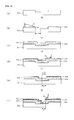
- FIG. 11 is a cross sectional diagram illustrating a structure and a forming process of an integrated thin-film solar cell formed by two slant depositions on a conductive substrate 101 according to another exemplary embodiment of the present invention.
- FIG. 11A an insulating film 101a is formed on the conductive substrate 101.
- a conductive material 102 is formed and patterned so that it is spaced a predetermined distance apart and insulated from each other on the insulating film 101 a.
- a solar cell (semiconductor) layer 103 is formed on the substrate comprising the conductive material 102.
- the solar cell layer 103 is etched using the first transparent conductive material 104 as a mask in FIG. 11E.
- a second transparent conductive material 105 is obliquely deposited on the substrate comprising the etched solar cell layer 103 to connect with the conductive material 102, thereby electrically connecting the solar cells with each other in series.
- the integrated thin-film solar cell according to the present invention is of a structure where the insulating film 101a, the conductive material 102, the solar cell (semiconductor) layer 103, the first transparent conductive material 104, and the second transparent conductive material 105 are sequentially layered on the conductive substrate 101.
- the conductive material 102 is patterned to have an insulating gap for insulation from left/right adjacent conductive materials 102.
- the solar cell (semiconductor) layer 103 and the first transparent conductive material 104 are deposited on the patterned conductive material 102.
- the second transparent conductive material 105 formed on the first transparent conductive material 104 is of a structure in which it gets in contact with the adjacent conductive material 102 of one direction, thereby accomplishing electrical serial connection between unit elements.
- the patterned conductive material 102 can have a slant section with a predetermined slope at its side portion. But, this is not intended to limit the scope of the present invention and thus, the patterned conductive material 102 can have a curved slant section or a section vertical with the substrate 101.
- the insulating film 101a should be formed on the substrate 101 because the substrate 101 has a conductive property.
- Other detailed descriptions of forming relation and content of the solar cell are the same as in the "(1) Integrated solar cell formed by two slant depositions on insulating substrate" and thus, will be omitted.
- FIG. 12 is a cross sectional diagram illustrating a structure and a forming process of an integrated thin-film solar cell formed by three slant depositions on an insulating substrate 201 according to a further another exemplary embodiment of the present invention.
- a first conductive material 202 is formed and patterned so that it is spaced a predetermined distance apart and insulated from each other on the insulating film 201.
- a second conductive material 203 is obliquely deposited on the substrate comprising the first conductive material 202.
- a solar cell (semiconductor) layer 204 is formed on the substrate comprising the second conductive material 203.
- the solar cell layer 204 is etched using the first transparent conductive material 205 as a mask in FIG. 12F.
- a second transparent conductive material 206 is obliquely deposited on the substrate comprising the etched solar cell layer 204 to connect with the second conductive material 203, thereby electrically connecting the solar cells with each other in series.
- the integrated thin-film solar cell according to the present invention is of a structure where the first conductive material 202, the second conductive material 203, the solar cell (semiconductor) layer 204, the first transparent conductive material 205, and the second transparent conductive material 206 are sequentially layered on the insulating substrate 101.
- the first conductive material 202 is patterned to have an insulating gap for insulation from left/right adjacent first conductive materials 202.
- the patterned first conductive material 202 can be vertical with the substrate 201 at its side portion as shown. But, this is not intended to limit the scope of the present invention and thus, the patterned first conductive material 202 can have a slant section with a predetermined slope or a curved slant section.
- the second transparent conductive material 206 formed on the first transparent conductive material 205 is of a structure in which it gets in contact with the adjacent second conductive material 203 of one direction, thereby accomplishing electrical serial connection between unit elements.
- a method of manufacturing the integrated thin-film solar cell will be described in sequence as follows.
- the patterned first conductive material 202 is formed on the insulating substrate 201 in a first process of the manufacturing method of the integrated thin-film solar cell according to the present invention.
- the insulating substrate 201 is a transparent substrate or a non-transparent substrate.
- the patterned first conductive material 202 is possible for all cases where surface prominence and depression is provided or not.
- the second conductive material 203 is deposited on a slant with a fifth angle ( ⁇ 5 ) on the substrate comprising the patterned first conductive material 202.
- a fifth angle ( ⁇ 5 ) on the substrate comprising the patterned first conductive material 202.
- the second conductive material 203 is deposited by the fifth angle ( ⁇ 5 )
- it is thinly deposited on the first conductive material 202 excluding a one-side vertical surface of the first conductive material 202 and a portion (1a) caused by the fifth angle ( ⁇ 5 ), owing to deposition straightness (2d).
- the first and second conductive materials 202 and 203 use a transparent conductive material that is any one or more selected from the group consisting of zinc oxide (ZnO), tin oxide (SnO 2 ), and Indium Tin Oxide (ITO), a single metal with a high reflectivity such as aluminum (Al), argentums (Ag), and aurum (Au), a multi metal being a mixture of aluminum (Al)/argentums (Ag), or a metallic material that is any one or more selected from the group consisting of argentums (Ag), aluminum (Al), and aurum (Au).
- a transparent conductive material that is any one or more selected from the group consisting of zinc oxide (ZnO), tin oxide (SnO 2 ), and Indium Tin Oxide (ITO)
- ZnO zinc oxide
- SnO 2 tin oxide
- ITO Indium Tin Oxide
- a single metal with a high reflectivity such as aluminum (Al), argentums (Ag),
- FIG. 12D illustrating a cross sectional diagram illustrating a state where the solar cell layer 204 is formed
- the solar cell layer 204 is formed in compliance to a surface shape of the resultant comprising the above deposited second conductive material 203.
- the solar cell can be any one or more of a silicon-based solar cell, a compound-based solar cell, an organic solar cell, a dry dye-sensitized solar cell, and an organic/inorganic complex solar cell.
- the silicon-based solar cell is any one of an amorphous silicon (a-Si:H) single junction solar cell, an a-Si:H/a-Si:H or a-Si:H/a-Si:H/a-Si:H multi-junction solar cell, an amorphous silicon-germanium (a-SiGe:H) single junction solar cell, an a-Si:H/a-SiGe:H double junction solar cell, an a-Si:H/a-SiGe:H/a-SiGe:H triple junction solar cell, an amorphous silicon/microcrystalline (polycrystalline) silicon double junction solar cell, and a protocrystalline silicon solar cell.
- a-Si:H amorphous silicon
- a-Si:H a-Si:H/a-Si:H or a-Si:H/a-Si:H/a-Si:H multi-junction solar cell
- FIG. 12E illustrating a cross sectional diagram of a state where the first transparent conductive material 205 is formed
- the first transparent conductive material 205 is obliquely deposited and formed on the above formed solar cell layer 204 using a deposition method such as electron beam or thermal deposition.
- the first transparent conductive material 205 is a transparent conductive material, and is at least one selected from the group consisting of zinc oxide (ZnO), tin oxide (SnO 2 ), and Indium Tin Oxide (ITO).
- ZnO zinc oxide
- SnO 2 tin oxide
- ITO Indium Tin Oxide
- the first transparent conductive material 205 when deposited on a slant with a sixth angle ( ⁇ 6 ) using an electron beam or thermal depositor, it is thinly deposited on the solar cell layer 204 excluding a one-side vertical surface of the solar cell layer 204 and a portion (1e) caused by the sixth angle ( ⁇ 6 ), owing to deposition straightness (2e).
- the portion (1e) comprising such a slant surface represents a region for etching implemented in the following step.
- FIG. 12F is a cross sectional diagram illustrating a vertical etching state with the first transparent conductive material 205 used as the mask.
- the above method can make it possible to minutely etch the solar cell layer 204 without needing a specific mask, thereby realizing an insulation gap of several ⁇ m to several tens of ⁇ m between the unit elements. This can reduce by more than tens of times to hundreds of times compared with conventional plasma-based chemical vaporization machining method and laser beam-based laser patterning method, thereby maximizing an effective area of the solar cell.
- the second transparent conductive material 206 is formed on the first transparent conductive material 205.
- the second transparent conductive material 206 is formed using the same deposition process as the first transparent conductive material 205 in a state where a predetermined insulating gap between the unit elements is provided in a previous etching process.
- the second transparent conductive material 206 when the second transparent conductive material 206 is deposited on a slant with a predetermined seventh angle ( ⁇ 7 ) using an electron beam or thermal depositor, it is thinly deposited on the first transparent conductive material 205 excluding one-side vertical surfaces of the first transparent conductive material 205 and the solar cell layer 204 and a portion (1e) caused by the slant angle ( ⁇ 7 ), owing to deposition straightness (2f).
- the second transparent conductive material 206 is a transparent conductive material, and is at least one selected from the group consisting of zinc oxide (ZnO), tin oxide (SnO 2 ), and Indium Tin Oxide (ITO).
- ZnO zinc oxide
- SnO 2 tin oxide
- ITO Indium Tin Oxide
- the second transparent conductive material 206 of a left unit element and the second conductive material 203 of a right unit element adjacent to the left unit element get in contact with each other, thereby achieving electrical serial connection between the unit elements.
- a metal line electrode is desirably formed and patterned to be spaced a predetermined distance apart from each other after the second transparent conductive material 206 is deposited. By forming so, the transparent conductive material can be enhanced in conductivity.
- the metal line is to improve a low conductivity of the transparent conductive material. In case where the transparent conductive material is formed, the metal line can be additionally formed anytime.
- the metal line uses a single metal with a high reflectivity such as aluminum (Al), argentums (Ag), and aurum (Au), a multi metal being a mixture of aluminum (Al)/argentums (Ag), or a metallic material that is any one or more selected from the group consisting of argentums (Ag), aluminum (Al), and aurum (Au).
- a single metal with a high reflectivity such as aluminum (Al), argentums (Ag), and aurum (Au)
- a multi metal being a mixture of aluminum (Al)/argentums (Ag)
- a metallic material that is any one or more selected from the group consisting of argentums (Ag), aluminum (Al), and aurum (Au).
- a method for patterning the conductive material on the substrate and other detailed descriptions of forming relation and content are the same as in the "(1) Integrated solar cell formed by two slant depositions on insulating substrate" and thus, will be omitted.
- FIG. 13 is a cross sectional diagram illustrating a structure and a forming process of an integrated thin-film solar cell formed by three slant depositions on a conductive substrate 201 according to a still another exemplary embodiment of the present invention.
- an insulating film 201 a is formed on the conductive substrate 201.
- a first conductive material 202 is formed and patterned so that it is spaced a predetermined distance apart and insulated from each other on the insulating film 201a.
- a second conductive material 203 is obliquely deposited on the substrate comprising the formed first conductive material 202.
- a solar cell (semiconductor) layer 204 is formed on the substrate comprising the deposited second conductive material 203.
- the solar cell layer 204 is etched using the first transparent conductive material 205 as a mask in FIG. 13F.
- a second transparent conductive material 206 is obliquely deposited on the substrate comprising the etched solar cell layer 204 to connect with the second conductive material 203, thereby electrically connecting the solar cells with each other in series.
- the integrated thin-film solar cell according to the present invention is of a structure where the insulating film 201a, the first conductive material 202, the second conductive material 203, the solar cell (semiconductor) layer 204, the first transparent conductive material 205, and the second transparent conductive material 206 are sequentially layered on the conductive substrate 201.
- the first conductive material 202 is patterned to have an insulating gap for insulation from left/right adjacent first conductive materials 202.
- the patterned first conductive material 202 can be vertical with the substrate 201 at its side portion as shown in FIG. 13G. But, this is not intended to limit the scope of the present invention and thus, the patterned first conductive material 202 can have a slant section with a predetermined slope or a curved slant section.
- the second transparent conductive material 206 formed on the first transparent conductive material 205 is of a structure in which it gets in contact with the adjacent second conductive material 203 of one direction, thereby accomplishing electrical serial connection between unit elements.
- the insulating film 201a should be formed on the substrate 201 because the substrate 201 has a conductive property.
- Other detailed descriptions of forming relation and content are the same as in the "(3) Integrated solar cell formed by three slant depositions on insulating substrate" and thus, will be omitted.
- Integrated solar cell formed by three slant depositions on insulating substrate with patterned prominence and depression surface.
- FIG. 14 is a cross sectional diagram illustrating a structure and a forming process of an integrated thin-film solar cell formed by three slant depositions on an insulating substrate 301 with patterned prominence and depression surface according to a yet another exemplary embodiment of the present invention.
- a conductive material 302 is obliquely deposited on the insulating substrate 301 with prominence and depression.
- a solar cell (semiconductor) layer 303 is formed on the substrate comprising the conductive material 302.
- the solar cell layer 303 is etched using the first transparent conductive material 304 as a mask in FIG. 14E.
- a second transparent conductive material 305 is obliquely deposited on the substrate comprising the etched solar cell layer 303 to connect with the conductive material 302, thereby electrically connecting the solar cells with each other in series.
- the integrated thin-film solar cell according to the present invention is of a structure where the conductive material 302, the solar cell (semiconductor) layer 303, the first transparent conductive material 304, and the second transparent conductive material 305 are sequentially layered on the insulating substrate 301 with the patterned prominence and depression surface.
- a side portion of prominence and depression can be vertical with the patterned prominence and depression surface of in the insulating substrate 301. But, this is not intended to limit the scope of the present invention and thus, the side portion can have a slant section with a predetermined slope or a curved slant section.
- the second transparent conductive material 305 formed on the first transparent conductive material 304 is of a structure in which it gets in contact with the adjacent conductive material 302 of one direction, thereby accomplishing electrical serial connection between unit elements.
- a method of manufacturing the integrated thin-film solar cell will be described in sequence as follows.
- the conductive material 302 is deposited on a slant with a fifth angle ( ⁇ 5 ) on the insulating substrate 301 with the prominence and depression in a first process of the manufacturing method of the integrated thin-film solar cell according to the present invention.
- the conductive material 302 is deposited by the fifth angle ( ⁇ 5 )
- it is thinly deposited on the insulating substrate 301 excluding a one-side vertical surface of the substrate 301 with the prominence and depression and a portion (1d) caused by the fifth angle ( ⁇ 5 ), owing to deposition straightness (2d).
- the conductive material 302 uses a transparent conductive material that is any one or more selected from the group consisting of zinc oxide (ZnO), tin oxide (SnO 2 ), and Indium Tin Oxide (ITO), a single metal with a high reflectivity such as aluminum (Al), argentums (Ag), and aurum (Au), a multi metal being a mixture of aluminum (Al)/argentums (Ag), or a metallic material that is any one or more selected from the group consisting of argentums (Ag), aluminum (Al), and aurum (Au).
- ZnO zinc oxide
- SnO 2 tin oxide
- ITO Indium Tin Oxide
- a single metal with a high reflectivity such as aluminum (Al), argentums (Ag), and aurum (Au)
- a multi metal being a mixture of aluminum (Al)/argentums (Ag)
- a metallic material that is any one or more selected from the group consisting of argentums (
- FIG. 14C illustrating a cross sectional diagram illustrating a state where the solar cell layer 303 is formed
- the solar cell layer 303 is formed in compliance to a surface shape of the resultant comprising the above deposited conductive material 302.
- the solar cell can be any one or more of a silicon-based solar cell, a compound-based solar cell, an organic solar cell, and a dry dye-sensitized solar cell.
- the silicon-based solar cell is any one of an amorphous silicon (a-Si:H) single junction solar cell, an a-Si:H/a-Si:H or a-Si:H/a-Si:H/a-Si:H multi-junction solar cell, an amorphous silicon-germanium (a-SiGe:H) single junction solar cell, an a-Si:H/a-SiGe:H double junction solar cell, an a-Si:H/a-SiGe:H/a-SiGe:H triple junction solar cell, an amorphous silicon/microcrystalline (polycrystalline) silicon double junction solar cell, and a protocrystalline silicon solar cell.
- a-Si:H amorphous silicon
- a-Si:H a-Si:H/a-Si:H or a-Si:H/a-Si:H/a-Si:H multi-junction solar cell
- FIG. 14D illustrating a cross sectional diagram of a state where the first transparent conductive material 304 is formed
- the first transparent conductive material 304 is obliquely deposited and formed on the above formed solar cell layer 303 using a deposition method such as electron beam or thermal deposition.
- the first transparent conductive material 304 is a transparent conductive material, and is at least one selected from the group consisting of zinc oxide (ZnO), tin oxide (SnO 2 ), and Indium Tin Oxide (ITO).
- ZnO zinc oxide
- SnO 2 tin oxide
- ITO Indium Tin Oxide
- the first transparent conductive material 304 is deposited on a slant with a sixth angle ( ⁇ 6 ) using an electron beam or thermal depositor as shown in FIG. 14D, it is thinly deposited on the solar cell layer 303 excluding a one-side vertical surface of the solar cell layer 303 and a portion (1e) caused by the sixth angle ( ⁇ 6 ), owing to deposition straightness (2e).
- the portion (1e) comprising such a slant surface represents a region for etching implemented in the following step.
- FIG. 14E is a cross sectional diagram illustrating a vertical etching state with the first transparent conductive material 304 used as the mask.
- the above method can make it possible to minutely etch the solar cell layer 303 without needing a specific mask, thereby realizing an insulation gap of several ⁇ m to several tens of ⁇ m between the unit elements. This can reduce by more than tens of times to hundreds of times compared with conventional plasma-based chemical vaporization machining method and laser beam-based laser patterning method, thereby maximizing an effective area of the solar cell.
- the second transparent conductive material 305 is formed on the first transparent conductive material 304.
- the second transparent conductive material 305 is formed using the same deposition process as the first transparent conductive material 304 in a state where a predetermined insulating gap between the unit elements is provided in a previous etching process.
- the second transparent conductive material 305 when the second transparent conductive material 305 is deposited on a slant with a predetermined seventh angle ( ⁇ 7 ) using an electron beam or thermal depositor, it is thinly deposited on the first transparent conductive material 304 excluding a one-side vertical surface of the solar cell layer 303 and a portion (1e) caused by the slant angle ( ⁇ 7 ), owing to deposition straightness (2f).
- the second transparent conductive material 305 is a transparent conductive material, and is at least one selected from the group consisting of zinc oxide (ZnO), tin oxide (SnO 2 ), and Indium Tin Oxide (ITO).
- ZnO zinc oxide
- SnO 2 tin oxide
- ITO Indium Tin Oxide
- the second transparent conductive material 305 of a left unit element and the conductive material 302 of a right unit element adjacent to the left unit element get in contact with each other, thereby achieving electrical serial connection between the unit elements.
- a metal line electrode is desirably formed and patterned to be spaced a predetermined distance apart from each other after the second transparent conductive material 305 is deposited. By forming so, the transparent conductive material can be enhanced in conductivity.
- the metal line is to improve a low conductivity of the transparent conductive material. In case where the transparent conductive material is formed, the metal line can be additionally formed anytime.
- the metal line uses a single metal with a high reflectivity such as aluminum (Al), argentums (Ag), and aurum (Au), a multi metal being a mixture of aluminum (Al)/argentums (Ag), or a metallic material that is any one or more selected from the group consisting of argentums (Ag), aluminum (Al), and aurum (Au).
- a single metal with a high reflectivity such as aluminum (Al), argentums (Ag), and aurum (Au)
- a multi metal being a mixture of aluminum (Al)/argentums (Ag)
- a metallic material that is any one or more selected from the group consisting of argentums (Ag), aluminum (Al), and aurum (Au).
- the substrate with the prominence and depression is formed by applying a hot-embossing method to a flat substrate.
- a method for patterning the conductive material on the substrate and other detailed descriptions of forming relation and content are the same as in the "(1) Integrated solar cell formed by two slant depositions on insulating substrate" and thus, will be omitted.
- Integrated solar cell formed by three slant depositions on conductive substrate with patterned prominence and depression surface.
- FIG. 15 is a cross sectional diagram illustrating a structure and a forming process of an integrated thin-film solar cell formed by three slant depositions on a conductive substrate 301 with patterned prominence and depression surface according to a yet another exemplary embodiment of the present invention.
- an insulating film 301a is formed on the conductive substrate 101.
- a conductive material 302 is formed and patterned so that it is spaced a predetermined distance apart and insulated from each other on the insulating film 301a.
- a solar cell (semiconductor) layer 303 is formed on the substrate comprising the conductive material 302.
- the solar cell layer 303 is etched using the first transparent conductive material 304 as a mask in FIG. 15E.
- a second transparent conductive material 305 is obliquely deposited on the substrate comprising the etched solar cell layer 303 to connect with the conductive material 302, thereby electrically connecting the solar cells with each other in series.
- the integrated thin-film solar cell according to the present invention is of a structure where the conductive material 302, the solar cell (semiconductor) layer 303, the first transparent conductive material 304, and the second transparent conductive material 305 are sequentially layered on the conductive substrate 301.
- a side portion of prominence and depression can be vertical with the patterned prominence and depression surface of in the conductive substrate 301. But, this is not intended to limit the scope of the present invention and thus, the side portion can have a slant section with a predetermined slope or a curved slant section.
- the second transparent conductive material 305 formed on the first transparent conductive material 304 is of a structure in which it gets in contact with the adjacent conductive material 302 of one direction, thereby accomplishing electrical serial connection between unit elements.
- a transparent electrode 202 is formed and patterned so that it is spaced a predetermined distance apart and insulated from each other on the transparent substrate 201.
- a transparent conductive material 203 is obliquely deposited on the substrate comprising the transparent electrode 202.
- a solar cell (semiconductor) layer 204 is formed on the substrate comprising the deposited transparent conductive material 203.
- Metal is obliquely deposited on the solar cell layer 204, thereby forming a first metal back electrode 205. After that, the solar cell layer 204 is etched using the first metal back electrode 205 as a mask.
- Metal is obliquely deposited on the substrate comprising the etched solar cell layer 204 to form and connect a second metal back electrode 206 with the transparent conductive material 203, thereby electrically connecting the solar cells with each other in series.
- the integrated thin-film solar cell according to the present invention is of a structure where the transparent electrode 202, the transparent conductive material 203, the solar cell (semiconductor) layer 204, the first metal back electrode 205, and the second metal back electrode 206 are sequentially layered on the transparent substrate 201.
- the transparent electrode 202 is patterned to have an insulating gap for insulation from left/right adjacent transparent electrodes 202.
- the patterned transparent electrode 202 can be vertical with the substrate 201 at its side portion as shown. But, this is not intended to limit the scope of the present invention and thus, the patterned transparent electrode 202 can have a slant section with a predetermined slope or a curved slant section.
- the second metal back electrode 206 formed on the first metal back electrode 205 is of a structure in which it gets in contact with the adjacent transparent conductive material 203 of one direction, thereby accomplishing electrical serial connection between unit elements.
- the first conductive material, the second conductive material, the first transparent conductive material, and the second transparent conductive material in FIG. 12 illustrating the " integrated thin-film solar cell formed by three slant depositions on insulating substrate" correspond to the transparent electrode, the transparent conductive material, the first metal back electrode, and the second metal back electrode in the "integrated thin-film solar cell formed by three slant depositions on transparent substrate", respectively.
- the transparent electrode and the transparent conductive material are a transparent conductive material, and is at least one selected from the group consisting of zinc oxide (ZnO), tin oxide (SnO 2 ), and Indium Tin Oxide (ITO).
- ZnO zinc oxide
- SnO 2 tin oxide
- ITO Indium Tin Oxide
- the first metal back electrode and the second metal back electrode are a single metal with a high reflectivity such as aluminum (Al), argentums (Ag), and aurum (Au), a multi metal being a mixture of aluminum (Al)/argentums (Ag), or a metallic material that is any one or more selected from the group consisting of argentums (Ag), aluminum (Al), and aurum (Au).
- Integrated solar cell formed by three slant depositions on transparent substrate with patterned prominence and depression surface.
- a transparent conductive material 302 is obliquely deposited on a transparent substrate 301 with a patterned prominence and depression surface.
- a solar cell (semiconductor) layer 303 is formed on the substrate comprising the deposited transparent conductive material 302.
- Metal is obliquely deposited on the solar cell layer 303, thereby forming a first metal back electrode 304. After that, the solar cell layer 303 is etched using the first metal back electrode 304 as a mask.
- Metal is obliquely deposited on the substrate comprising the etched solar cell layer 303 to form and connect a second metal back electrode 305 with the transparent conductive material 302, thereby electrically connecting the solar cells with each other in series.
- the integrated thin-film solar cell according to the present invention is of a structure where the transparent conductive material 302, the solar cell (semiconductor) layer 303, the first metal back electrode 304, and the second metal back electrode 305 are sequentially layered on the transparent substrate 301.
- a side portion of prominence and depression can be vertical with the patterned prominence and depression surface of in the transparent substrate 301. But, this is not intended to limit the scope of the present invention and thus, the side portion can have a slant section with a predetermined slope or a curved slant section.
- the second metal back electrode 305 formed on the first metal back electrode 304 is of a structure in which it gets in contact with the adjacent transparent conductive material 302 of one direction, thereby accomplishing electrical serial connection between unit elements.
- the conductive material, the first transparent conductive material, and the second transparent conductive material in the "(5) integrated thin-film solar cell formed by three slant depositions on insulating substrate with patterned prominence and depression surface" correspond to the transparent conductive material, the first metal back electrode, and the second metal back electrode in the "integrated thin-film solar cell formed by three slant depositions on transparent substrate", respectively.
- the transparent electrode and the transparent conductive material are a transparent conductive material, and is at least one selected from the group consisting of zinc oxide (ZnO), tin oxide (SnO 2 ), and Indium Tin Oxide (ITO).
- ZnO zinc oxide
- SnO 2 tin oxide
- ITO Indium Tin Oxide
- the first metal back electrode and the second metal back electrode are a single metal with a high reflectivity such as aluminum (Al), argentums (Ag), and aurum (Au), a multi metal being a mixture of aluminum (Al)/argentums (Ag), or a metallic material that is any one or more selected from the group consisting of argentums (Ag), aluminum (Al), and aurum (Au).
- the present invention has an effect that the insulation gap between the unit elements of the integrated thin-film solar cell can reduce by tens of times to hundreds of times compared with the conventional laser patterning and chemical vaporization machining method, thereby maximizing the effective area of the solar cell and thus, improving a performance of the unit cell of the solar cell.
- the present invention has an effect that a self alignment is possible, thereby making a precision position control unit unnecessary, and the printing method is used at the time of machining the transparent electrode, thereby making an expensive equipment such as a laser and a precision position control system unnecessary and thus, reducing the manufacturing cost, and the unit cell can be prevented from being deteriorated in performance due to its exposure to the atmosphere because all processes after the forming of the transparent electrode are performed under vacuum.
Landscapes
- Engineering & Computer Science (AREA)
- Microelectronics & Electronic Packaging (AREA)
- Electromagnetism (AREA)
- General Physics & Mathematics (AREA)
- Condensed Matter Physics & Semiconductors (AREA)
- Computer Hardware Design (AREA)
- Physics & Mathematics (AREA)
- Power Engineering (AREA)
- Life Sciences & Earth Sciences (AREA)
- Sustainable Development (AREA)
- Sustainable Energy (AREA)
- Manufacturing & Machinery (AREA)
- Photovoltaic Devices (AREA)
- Physical Vapour Deposition (AREA)
Applications Claiming Priority (1)
| Application Number | Priority Date | Filing Date | Title |
|---|---|---|---|
| KR1020050123337A KR100656738B1 (ko) | 2005-12-14 | 2005-12-14 | 집적형 박막 태양전지 및 그 제조 방법 |
Publications (2)
| Publication Number | Publication Date |
|---|---|
| EP1798778A2 true EP1798778A2 (de) | 2007-06-20 |
| EP1798778A3 EP1798778A3 (de) | 2012-05-16 |
Family
ID=37733064
Family Applications (1)
| Application Number | Title | Priority Date | Filing Date |
|---|---|---|---|
| EP06025934A Withdrawn EP1798778A3 (de) | 2005-12-14 | 2006-12-14 | Integrierte Dünnfilm-Solarzelle und Verfahren zu ihrer Herstellung |
Country Status (5)
| Country | Link |
|---|---|
| US (3) | US8148626B2 (de) |
| EP (1) | EP1798778A3 (de) |
| JP (1) | JP4796947B2 (de) |
| KR (1) | KR100656738B1 (de) |
| CN (1) | CN1983568B (de) |
Cited By (6)
| Publication number | Priority date | Publication date | Assignee | Title |
|---|---|---|---|---|
| EP2081234A2 (de) | 2008-01-09 | 2009-07-22 | LG Electronics Inc. | Dünnfilmsolarzellen und Herstellungsverfahren dafür |
| EP2405328A2 (de) * | 2009-03-04 | 2012-01-11 | Dong Sik Nam | Berührungsbildschirmsensor |
| AT512677A1 (de) * | 2012-03-30 | 2013-10-15 | Oesterreichisches Forschungs Und Pruefzentrum Arsenal Ges M B H | Herstellungsverfahren strukturierter Dünnschicht Photovoltaik |
| EP2668667A1 (de) * | 2011-01-24 | 2013-12-04 | LG Innotek Co., Ltd. | Solarzelle und verfahren zu ihrer herstellung |
| WO2014188092A1 (fr) * | 2013-05-23 | 2014-11-27 | Sunpartner Technologies | Mono cellule photovoltaïque semi-transparente en couches minces |
| EP3091584A4 (de) * | 2013-12-31 | 2017-09-06 | Korea Advanced Institute Of Science And Technology | Vorrichtung zur herstellung einer integrierten dünnschichtsolarzelle |
Families Citing this family (35)
| Publication number | Priority date | Publication date | Assignee | Title |
|---|---|---|---|---|
| JP4981020B2 (ja) * | 2005-03-16 | 2012-07-18 | コリア アドバンスト インスティテュート オブ サイエンス アンド テクノロジー | 集積型薄膜太陽電池、その製造方法と集積型薄膜太陽電池用透明電極の加工方法、その構造及びその透明電極が形成された透明基板 |
| KR100725110B1 (ko) * | 2005-12-14 | 2007-06-04 | 한국과학기술원 | 투과형 집적형 박막 태양전지 및 그 제조 방법. |
| KR100656738B1 (ko) * | 2005-12-14 | 2006-12-14 | 한국과학기술원 | 집적형 박막 태양전지 및 그 제조 방법 |
| KR101476125B1 (ko) * | 2008-10-02 | 2014-12-26 | 주성엔지니어링(주) | 박막형 태양전지 및 그 제조방법 |
| US20100126583A1 (en) * | 2008-11-25 | 2010-05-27 | Jeongwoo Lee | Thin film solar cell and method of manufacturing the same |
| US8330040B2 (en) * | 2008-12-03 | 2012-12-11 | Applied Materials, Inc. | Photovoltaic cells including spaced ramps and methods of manufacture |
| TWI422048B (zh) * | 2008-12-03 | 2014-01-01 | Applied Materials Inc | 包括間隔斜坡之光伏電池及其製造方法 |
| US8541680B2 (en) * | 2008-12-03 | 2013-09-24 | Applied Materials, Inc. | Photovoltaic cells including peaks and methods of manufacture |
| KR101573675B1 (ko) * | 2008-12-19 | 2015-12-03 | 주성엔지니어링(주) | 박막형 태양전지 및 그 제조 방법 |
| KR20100090046A (ko) * | 2009-02-05 | 2010-08-13 | 엘지디스플레이 주식회사 | 박막 태양전지 및 그 제조방법 |
| KR101028971B1 (ko) | 2009-05-26 | 2011-04-19 | 한국과학기술원 | 집적형 박막 태양전지 및 그의 제조 방법 |
| US20120073644A1 (en) * | 2009-06-12 | 2012-03-29 | Seung-Yeop Myong | Photovoltaic Device |
| US20120067416A1 (en) * | 2009-06-12 | 2012-03-22 | Seung-Yeop Myong | Photovoltaic Device |
| US20120037225A1 (en) * | 2009-06-16 | 2012-02-16 | Lg Innotek Co., Ltd. | Solar cell and method of fabricating the same |
| KR101112487B1 (ko) * | 2009-08-06 | 2012-03-09 | 한국과학기술원 | 광기전력 장치 및 그 제조 방법 |
| KR101210168B1 (ko) * | 2010-03-24 | 2012-12-07 | 엘지이노텍 주식회사 | 태양광 발전장치 및 이의 제조방법 |
| DE112010005449T5 (de) * | 2010-04-05 | 2013-04-18 | Mitsubishi Electric Corporation | Substrat für eine fotoelektrische Wandlervorrichtung und Verfahren zur Herstellung des Substrats, fotoelektrische Dünnschichtwandlervorrichtung und Verfahren zur Herstellung der fotoelektrischen Dünnschichtwandlervorrichtung, und Solarzellenmodul |
| KR101060239B1 (ko) * | 2010-08-26 | 2011-08-29 | 한국과학기술원 | 집적형 박막 광기전력 소자 및 그의 제조 방법 |
| US8236604B2 (en) * | 2010-09-03 | 2012-08-07 | Tetrasun, Inc. | Fine line metallization of photovoltaic devices by partial lift-off of optical coatings |
| KR101189432B1 (ko) | 2011-01-25 | 2012-10-10 | 엘지이노텍 주식회사 | 태양전지 및 이의 제조방법 |
| US9070810B2 (en) * | 2011-02-04 | 2015-06-30 | Azur Space Solar Power Gmbh | Multiple solar cell and method for manufacturing the same |
| DE102011000521A1 (de) | 2011-02-04 | 2012-08-23 | Azur Space Solar Power Gmbh | Mehrfachsolarzelle sowie Verfahren zur Herstellung einer solchen |
| KR20130014968A (ko) * | 2011-08-01 | 2013-02-12 | 엘지이노텍 주식회사 | 태양전지 및 이의 제조방법 |
| JP2013183065A (ja) * | 2012-03-02 | 2013-09-12 | Idemitsu Kosan Co Ltd | 有機薄膜太陽電池 |
| KR101349411B1 (ko) * | 2012-04-02 | 2014-01-10 | 엘지이노텍 주식회사 | 태양전지 및 이의 제조방법 |
| KR101301003B1 (ko) * | 2012-04-30 | 2013-08-28 | 에스엔유 프리시젼 주식회사 | 박막 태양전지 제조방법 및 이를 이용하는 박막 태양전지 |
| KR101382880B1 (ko) * | 2012-07-31 | 2014-04-09 | 엘지이노텍 주식회사 | 태양광 발전장치 및 이의 제조방법 |
| KR102042026B1 (ko) | 2013-06-20 | 2019-11-27 | 엘지이노텍 주식회사 | 태양전지 |
| CN103700670B (zh) * | 2013-12-20 | 2016-08-17 | 京东方科技集团股份有限公司 | 阵列基板及其制作方法、显示装置 |
| US20150372173A1 (en) * | 2014-06-24 | 2015-12-24 | University Of Florida Research Foundation, Inc. | Graded transparent conducting oxide (g-tco) for thin film solar cells |
| US9673341B2 (en) | 2015-05-08 | 2017-06-06 | Tetrasun, Inc. | Photovoltaic devices with fine-line metallization and methods for manufacture |
| AT518892B1 (de) * | 2017-02-07 | 2018-02-15 | Joanneum Res Forschungsgmbh | Verfahren zur Herstellung eines Photovoltaikbauteils und Photovoltaikbaustein |
| CN111244211A (zh) * | 2018-11-29 | 2020-06-05 | 中国科学院大连化学物理研究所 | 一种飞艇光伏材料器件一体化结构及制备方法 |
| CN110277473B (zh) * | 2019-05-31 | 2024-03-26 | 信利半导体有限公司 | 一种薄膜光伏电池的制造方法及薄膜光伏电池 |
| CN113272987A (zh) * | 2019-12-12 | 2021-08-17 | 株式会社安能科多科技 | 元件的制造方法 |
Family Cites Families (45)
| Publication number | Priority date | Publication date | Assignee | Title |
|---|---|---|---|---|
| US3994012A (en) * | 1975-05-07 | 1976-11-23 | The Regents Of The University Of Minnesota | Photovoltaic semi-conductor devices |
| US4200472A (en) * | 1978-06-05 | 1980-04-29 | The Regents Of The University Of California | Solar power system and high efficiency photovoltaic cells used therein |
| US4292092A (en) * | 1980-06-02 | 1981-09-29 | Rca Corporation | Laser processing technique for fabricating series-connected and tandem junction series-connected solar cells into a solar battery |
| US4514582A (en) | 1982-09-17 | 1985-04-30 | Exxon Research And Engineering Co. | Optical absorption enhancement in amorphous silicon deposited on rough substrate |
| US4501636A (en) * | 1983-12-28 | 1985-02-26 | The United States Of America As Represented By The Secretary Of The Air Force | Apparatus for etching vertical junction solar cell wafers |
| JPS60182757A (ja) | 1984-02-29 | 1985-09-18 | Kanegafuchi Chem Ind Co Ltd | 集積型太陽電池 |
| JPS6135573A (ja) * | 1984-07-27 | 1986-02-20 | Matsushita Electric Ind Co Ltd | 光起電力素子の製造法 |
| JPS6254971A (ja) * | 1985-09-04 | 1987-03-10 | Sanyo Electric Co Ltd | 光起電力装置 |
| JPS62142368A (ja) * | 1985-12-17 | 1987-06-25 | Fuji Electric Co Ltd | 薄膜半導体装置の製造方法 |
| DE3604917A1 (de) | 1986-02-17 | 1987-08-27 | Messerschmitt Boelkow Blohm | Verfahren zur herstellung eines integrierten verbandes in reihe geschalteter duennschicht-solarzellen |
| JPS6342180A (ja) | 1986-08-08 | 1988-02-23 | Toa Nenryo Kogyo Kk | 集積型光起電力装置の製造方法 |
| US4740431A (en) | 1986-12-22 | 1988-04-26 | Spice Corporation | Integrated solar cell and battery |
| US5294869A (en) * | 1991-12-30 | 1994-03-15 | Eastman Kodak Company | Organic electroluminescent multicolor image display device |
| JP2755281B2 (ja) | 1992-12-28 | 1998-05-20 | 富士電機株式会社 | 薄膜太陽電池およびその製造方法 |
| JPH07202229A (ja) | 1994-07-07 | 1995-08-04 | Semiconductor Energy Lab Co Ltd | 選択的被膜形成方法 |
| JPH08274360A (ja) | 1995-03-30 | 1996-10-18 | Japan Energy Corp | 光電変換半導体装置の製造方法 |
| KR0175359B1 (ko) * | 1995-12-15 | 1999-02-01 | 양승택 | 초전도체-절연체-초전도체 조셉슨 터널 접합구조의 제조방법 |
| JPH09260695A (ja) * | 1996-03-19 | 1997-10-03 | Canon Inc | 光起電力素子アレーの製造方法 |
| JP3436858B2 (ja) | 1997-02-27 | 2003-08-18 | シャープ株式会社 | 薄膜太陽電池の製造方法 |
| US6207890B1 (en) * | 1997-03-21 | 2001-03-27 | Sanyo Electric Co., Ltd. | Photovoltaic element and method for manufacture thereof |
| JPH1126793A (ja) | 1997-06-30 | 1999-01-29 | Dainippon Printing Co Ltd | 薄膜太陽電池セルパターンの形成法 |
| DE19741832A1 (de) * | 1997-09-23 | 1999-03-25 | Inst Solarenergieforschung | Verfahren zur Herstellung einer Solarzelle und Solarzelle |
| JPH1197723A (ja) | 1997-09-25 | 1999-04-09 | Citizen Watch Co Ltd | 太陽電池および太陽電池の製造方法 |
| JPH11112010A (ja) * | 1997-10-08 | 1999-04-23 | Sharp Corp | 太陽電池およびその製造方法 |
| JPH11312860A (ja) | 1998-04-27 | 1999-11-09 | Jsr Corp | 電極の製造方法および転写フィルム |
| DE19819200B4 (de) | 1998-04-29 | 2006-01-05 | Fraunhofer-Gesellschaft zur Förderung der angewandten Forschung e.V. | Solarzelle mit Kontaktstrukturen und Verfahren zur Herstellung der Kontaktstrukturen |
| JP3940546B2 (ja) | 1999-06-07 | 2007-07-04 | 株式会社東芝 | パターン形成方法およびパターン形成材料 |
| DE10017610C2 (de) | 2000-03-30 | 2002-10-31 | Hahn Meitner Inst Berlin Gmbh | Verfahren zur Herstellung eines Solarmoduls mit integriert serienverschalteten Dünnschicht-Solarzellen und Verwendung davon |
| KR20020005152A (ko) | 2000-07-08 | 2002-01-17 | 구본준, 론 위라하디락사 | 투명도전막 패터닝 방법 |
| DE10103114A1 (de) * | 2001-01-24 | 2002-10-31 | Univ Stuttgart | Herstellen elektrischer Verbindungen in Substratöffnungen von Schaltungseinheiten mittels gerichteter Abscheidung leitfähiger Schichten |
| CN1291502C (zh) | 2001-03-19 | 2006-12-20 | 信越半导体株式会社 | 太阳能电池及其制造方法 |
| DE10142481A1 (de) | 2001-08-31 | 2003-03-27 | Rudolf Hezel | Solarzelle sowie Verfahren zur Herstellung einer solchen |
| EP1357602A1 (de) * | 2002-03-19 | 2003-10-29 | Scheuten Glasgroep | Selbstjustierende Serienverschaltung von Dünnschichten und Verfahren zur Herstellung |
| US6660930B1 (en) * | 2002-06-12 | 2003-12-09 | Rwe Schott Solar, Inc. | Solar cell modules with improved backskin |
| US20040118444A1 (en) * | 2002-12-20 | 2004-06-24 | General Electric Company | Large-area photovoltaic devices and methods of making same |
| WO2004064167A1 (ja) | 2003-01-10 | 2004-07-29 | Kaneka Corporation | 透光性薄膜太陽電池モジュールおよびその製造方法 |
| JP2005101384A (ja) * | 2003-09-26 | 2005-04-14 | Sanyo Electric Co Ltd | 光起電力装置及びその製造方法 |
| JP2005197537A (ja) * | 2004-01-09 | 2005-07-21 | Matsushita Electric Ind Co Ltd | 集積型薄膜太陽電池およびその製造方法 |
| JP4981020B2 (ja) * | 2005-03-16 | 2012-07-18 | コリア アドバンスト インスティテュート オブ サイエンス アンド テクノロジー | 集積型薄膜太陽電池、その製造方法と集積型薄膜太陽電池用透明電極の加工方法、その構造及びその透明電極が形成された透明基板 |
| KR100756286B1 (ko) * | 2005-03-16 | 2007-09-06 | 한국과학기술원 | 집적형 박막 태양전지 및 그 제조 방법 |
| KR100656738B1 (ko) | 2005-12-14 | 2006-12-14 | 한국과학기술원 | 집적형 박막 태양전지 및 그 제조 방법 |
| KR100725110B1 (ko) * | 2005-12-14 | 2007-06-04 | 한국과학기술원 | 투과형 집적형 박막 태양전지 및 그 제조 방법. |
| US20100185574A1 (en) * | 2009-01-16 | 2010-07-22 | Sondre Skatter | Network mechanisms for a risk based interoperability standard for security systems |
| KR101028971B1 (ko) * | 2009-05-26 | 2011-04-19 | 한국과학기술원 | 집적형 박막 태양전지 및 그의 제조 방법 |
| KR101112487B1 (ko) * | 2009-08-06 | 2012-03-09 | 한국과학기술원 | 광기전력 장치 및 그 제조 방법 |
-
2005
- 2005-12-14 KR KR1020050123337A patent/KR100656738B1/ko not_active IP Right Cessation
-
2006
- 2006-12-13 US US11/610,254 patent/US8148626B2/en not_active Expired - Fee Related
- 2006-12-13 JP JP2006335721A patent/JP4796947B2/ja not_active Expired - Fee Related
- 2006-12-14 CN CN2006101658589A patent/CN1983568B/zh not_active Expired - Fee Related
- 2006-12-14 EP EP06025934A patent/EP1798778A3/de not_active Withdrawn
-
2009
- 2009-09-28 US US12/568,360 patent/US8168882B2/en not_active Expired - Fee Related
- 2009-09-28 US US12/568,370 patent/US8153885B2/en not_active Expired - Fee Related
Non-Patent Citations (1)
| Title |
|---|
| None |
Cited By (14)
| Publication number | Priority date | Publication date | Assignee | Title |
|---|---|---|---|---|
| EP2081234A2 (de) | 2008-01-09 | 2009-07-22 | LG Electronics Inc. | Dünnfilmsolarzellen und Herstellungsverfahren dafür |
| EP2081234A3 (de) * | 2008-01-09 | 2012-08-15 | LG Electronics Inc. | Dünnfilmsolarzellen und Herstellungsverfahren dafür |
| EP2405328A2 (de) * | 2009-03-04 | 2012-01-11 | Dong Sik Nam | Berührungsbildschirmsensor |
| EP2405328A4 (de) * | 2009-03-04 | 2013-10-02 | Dong Sik Nam | Berührungsbildschirmsensor |
| EP2668667A4 (de) * | 2011-01-24 | 2014-06-25 | Lg Innotek Co Ltd | Solarzelle und verfahren zu ihrer herstellung |
| EP2668667A1 (de) * | 2011-01-24 | 2013-12-04 | LG Innotek Co., Ltd. | Solarzelle und verfahren zu ihrer herstellung |
| AT512677B1 (de) * | 2012-03-30 | 2013-12-15 | Oesterreichisches Forschungs Und Pruefzentrum Arsenal Ges M B H | Herstellungsverfahren strukturierter Dünnschicht Photovoltaik |
| AT512677A1 (de) * | 2012-03-30 | 2013-10-15 | Oesterreichisches Forschungs Und Pruefzentrum Arsenal Ges M B H | Herstellungsverfahren strukturierter Dünnschicht Photovoltaik |
| WO2014188092A1 (fr) * | 2013-05-23 | 2014-11-27 | Sunpartner Technologies | Mono cellule photovoltaïque semi-transparente en couches minces |
| CN105378940A (zh) * | 2013-05-23 | 2016-03-02 | 太阳伙伴科技公司 | 薄层半透明光伏单电池 |
| CN105378940B (zh) * | 2013-05-23 | 2018-12-14 | 太阳伙伴科技公司 | 薄层半透明光伏单电池 |
| US10770608B2 (en) | 2013-05-23 | 2020-09-08 | Garmin Switzerland Gmbh | Semi-transparent thin-film photovoltaic mono cell |
| US11424378B2 (en) | 2013-05-23 | 2022-08-23 | Garmin Switzerland Gmbh | Thin-film photovoltaic cell |
| EP3091584A4 (de) * | 2013-12-31 | 2017-09-06 | Korea Advanced Institute Of Science And Technology | Vorrichtung zur herstellung einer integrierten dünnschichtsolarzelle |
Also Published As
| Publication number | Publication date |
|---|---|
| US20100018574A1 (en) | 2010-01-28 |
| US8153885B2 (en) | 2012-04-10 |
| US8168882B2 (en) | 2012-05-01 |
| US20100012173A1 (en) | 2010-01-21 |
| CN1983568B (zh) | 2011-11-23 |
| US20070131271A1 (en) | 2007-06-14 |
| JP2007165903A (ja) | 2007-06-28 |
| US8148626B2 (en) | 2012-04-03 |
| CN1983568A (zh) | 2007-06-20 |
| KR100656738B1 (ko) | 2006-12-14 |
| JP4796947B2 (ja) | 2011-10-19 |
| EP1798778A3 (de) | 2012-05-16 |
Similar Documents
| Publication | Publication Date | Title |
|---|---|---|
| US8148626B2 (en) | Integrated thin-film solar cell and method of manufacturing the same | |
| US8449782B2 (en) | See-through-type integrated thin-film solar cell, method of manufacturing the same and method of electrically series connecting unit cells thereof | |
| KR100756286B1 (ko) | 집적형 박막 태양전지 및 그 제조 방법 | |
| US7927497B2 (en) | Integrated thin-film solar cells and method of manufacturing thereof and processing method of transparent electrode for integrated thin-film solar cells and structure thereof, and transparent substrate having processed transparent electrode | |
| US20180175234A1 (en) | Array Of Monolithically Integrated Thin Film Photovoltaic Cells And Associated Methods | |
| CN100570903C (zh) | 集成薄膜太阳能电池及其制造方法、及集成薄膜太阳能电池的透明电极的处理方法及其结构、及具有处理过的透明电极的透明基板 | |
| US20100300525A1 (en) | Integrated thin-film solar cell and manufacturing method thereof | |
| US8802969B2 (en) | Photovoltaic device and method for manufacturing thereof | |
| US20120048342A1 (en) | Integrated thin-film photovoltaic device and manufacturing method thereof | |
| US20100252109A1 (en) | Thin film type solar cell and method for manufacturing the same | |
| KR101425886B1 (ko) | 박막형 태양전지 및 그 제조방법 | |
| KR101000383B1 (ko) | 집적형 박막 태양전지 및 그 제조 방법 | |
| KR101000380B1 (ko) | 집적형 박막 태양전지 및 그 제조 방법 |
Legal Events
| Date | Code | Title | Description |
|---|---|---|---|
| PUAI | Public reference made under article 153(3) epc to a published international application that has entered the european phase |
Free format text: ORIGINAL CODE: 0009012 |
|
| AK | Designated contracting states |
Kind code of ref document: A2 Designated state(s): AT BE BG CH CY CZ DE DK EE ES FI FR GB GR HU IE IS IT LI LT LU LV MC NL PL PT RO SE SI SK TR |
|
| AX | Request for extension of the european patent |
Extension state: AL BA HR MK YU |
|
| PUAL | Search report despatched |
Free format text: ORIGINAL CODE: 0009013 |
|
| AK | Designated contracting states |
Kind code of ref document: A3 Designated state(s): AT BE BG CH CY CZ DE DK EE ES FI FR GB GR HU IE IS IT LI LT LU LV MC NL PL PT RO SE SI SK TR |
|
| AX | Request for extension of the european patent |
Extension state: AL BA HR MK RS |
|
| RIC1 | Information provided on ipc code assigned before grant |
Ipc: H01L 27/142 20060101ALI20120410BHEP Ipc: H01L 31/18 20060101AFI20120410BHEP |
|
| 17P | Request for examination filed |
Effective date: 20121114 |
|
| AKX | Designation fees paid |
Designated state(s): AT BE BG CH CY CZ DE DK EE ES FI FR GB GR HU IE IS IT LI LT LU LV MC NL PL PT RO SE SI SK TR |
|
| 17Q | First examination report despatched |
Effective date: 20130114 |
|
| STAA | Information on the status of an ep patent application or granted ep patent |
Free format text: STATUS: THE APPLICATION IS DEEMED TO BE WITHDRAWN |
|
| 18D | Application deemed to be withdrawn |
Effective date: 20140701 |