EP1779438B2 - Iii-v-hemt-bauelemente - Google Patents
Iii-v-hemt-bauelemente Download PDFInfo
- Publication number
- EP1779438B2 EP1779438B2 EP05755884.3A EP05755884A EP1779438B2 EP 1779438 B2 EP1779438 B2 EP 1779438B2 EP 05755884 A EP05755884 A EP 05755884A EP 1779438 B2 EP1779438 B2 EP 1779438B2
- Authority
- EP
- European Patent Office
- Prior art keywords
- layer
- iii
- top surface
- gan
- nitride semiconductor
- Prior art date
- Legal status (The legal status is an assumption and is not a legal conclusion. Google has not performed a legal analysis and makes no representation as to the accuracy of the status listed.)
- Expired - Lifetime
Links
Images


Classifications
-
- H—ELECTRICITY
- H10—SEMICONDUCTOR DEVICES; ELECTRIC SOLID-STATE DEVICES NOT OTHERWISE PROVIDED FOR
- H10D—INORGANIC ELECTRIC SEMICONDUCTOR DEVICES
- H10D30/00—Field-effect transistors [FET]
- H10D30/40—FETs having zero-dimensional [0D], one-dimensional [1D] or two-dimensional [2D] charge carrier gas channels
- H10D30/47—FETs having zero-dimensional [0D], one-dimensional [1D] or two-dimensional [2D] charge carrier gas channels having two-dimensional [2D] charge carrier gas channels, e.g. nanoribbon FETs or high electron mobility transistors [HEMT]
-
- H—ELECTRICITY
- H10—SEMICONDUCTOR DEVICES; ELECTRIC SOLID-STATE DEVICES NOT OTHERWISE PROVIDED FOR
- H10D—INORGANIC ELECTRIC SEMICONDUCTOR DEVICES
- H10D30/00—Field-effect transistors [FET]
- H10D30/01—Manufacture or treatment
- H10D30/015—Manufacture or treatment of FETs having heterojunction interface channels or heterojunction gate electrodes, e.g. HEMT
-
- H—ELECTRICITY
- H10—SEMICONDUCTOR DEVICES; ELECTRIC SOLID-STATE DEVICES NOT OTHERWISE PROVIDED FOR
- H10D—INORGANIC ELECTRIC SEMICONDUCTOR DEVICES
- H10D30/00—Field-effect transistors [FET]
- H10D30/40—FETs having zero-dimensional [0D], one-dimensional [1D] or two-dimensional [2D] charge carrier gas channels
- H10D30/47—FETs having zero-dimensional [0D], one-dimensional [1D] or two-dimensional [2D] charge carrier gas channels having two-dimensional [2D] charge carrier gas channels, e.g. nanoribbon FETs or high electron mobility transistors [HEMT]
- H10D30/471—High electron mobility transistors [HEMT] or high hole mobility transistors [HHMT]
- H10D30/475—High electron mobility transistors [HEMT] or high hole mobility transistors [HHMT] having wider bandgap layer formed on top of lower bandgap active layer, e.g. undoped barrier HEMTs such as i-AlGaN/GaN HEMTs
- H10D30/4755—High electron mobility transistors [HEMT] or high hole mobility transistors [HHMT] having wider bandgap layer formed on top of lower bandgap active layer, e.g. undoped barrier HEMTs such as i-AlGaN/GaN HEMTs having wide bandgap charge-carrier supplying layers, e.g. modulation doped HEMTs such as n-AlGaAs/GaAs HEMTs
-
- H—ELECTRICITY
- H10—SEMICONDUCTOR DEVICES; ELECTRIC SOLID-STATE DEVICES NOT OTHERWISE PROVIDED FOR
- H10D—INORGANIC ELECTRIC SEMICONDUCTOR DEVICES
- H10D64/00—Electrodes of devices having potential barriers
- H10D64/01—Manufacture or treatment
- H10D64/011—Manufacture or treatment of electrodes ohmically coupled to a semiconductor
-
- H—ELECTRICITY
- H10—SEMICONDUCTOR DEVICES; ELECTRIC SOLID-STATE DEVICES NOT OTHERWISE PROVIDED FOR
- H10D—INORGANIC ELECTRIC SEMICONDUCTOR DEVICES
- H10D62/00—Semiconductor bodies, or regions thereof, of devices having potential barriers
- H10D62/80—Semiconductor bodies, or regions thereof, of devices having potential barriers characterised by the materials
- H10D62/85—Semiconductor bodies, or regions thereof, of devices having potential barriers characterised by the materials being Group III-V materials, e.g. GaAs
- H10D62/8503—Nitride Group III-V materials, e.g. AlN or GaN
Definitions
- This invention relates to normally-off type semiconductor devices comprising III-V semiconductors.
- the WO 01/57929 A1 discloses new group III nitride based field effect transistors and high electron mobility transistors that provide enhanced high frequency response characteristics.
- the preferred transistors are made from GaN/AlGaN and have a dielectric layer and the surface of their barrier layer.
- the dielectric layer has a high percentage of donor electrons that neutralize traps in the barrier layer such that the traps cannot slow the high frequency response of the transistors.
- a new method of manufacturing the transistors is also disclosed, with the new method using sputtering to deposit a dielectric layer.
- III-V semiconductors have a high breakdown field and a high saturated electron mobility, it is expected that semiconductor devices comprising III-V semiconductors will have a high breakdown voltage and will control large currents.
- Current research includes research on semiconductor devices that have a heterostructure comprising gallium nitride (GaN), an example of which is disclosed in Japanese Laid-Open Patent Application Publication No. 2003- 59946 .
- GaN gallium nitride
- One of this type of semiconductor devices is an HEMT (High Electron Mobility Transistor) having a heterostructure comprising a p-GaN layer, and an n-AlGaN layer stacked on a top surface of the p-GaN layer. Since aluminum (Al) is contained in semiconducting crystals of the n-AlGaN layer, a band gap of this layer is wider than the p-GaN layer.
- a drain electrode, a gate electrode, and a source electrode are formed at a top surface of the n-AlGaN layer. The gate electrode is formed between the drain electrode and the source electrode.
- a potential well is formed by the p-GaN layer and the n-AlGaN layer at their junction, however, an energy level of conduction band of the potential well is above the Fermi level unless a positive gate voltage is not applied to the gate electrode. Consequently 2DEG (2 Dimensional Electron Gas) is not generated in the potential well while the gate voltage is not being applied to the gate electrode. As a result, normally-off operation of the HEMT is possible. While a predetermined on-voltage is applied to the gate electrode, the energy level of conduction band of the potential well becomes lower than the Fermi level, and the 2DEG is generated in the potential well. Since electrons in the 2DEG move within the potential well, electric currents flow between the drain electrode to the source electrode while the predetermined gate voltage is being applied to the gate electrode of HEMT.
- the on-resistance means a magnitude of resistance between the drain electrode and the source electrode while the predetermined gate voltage is applied to the gate electrode of HEMT.
- a countermeasure has been considered of reducing impurity concentration in the p-GaN layer so as to reduce the on-resistance.
- the impurity concentration in the p-GaN layer is reduced, the energy level of the potential well could approach the Fermi level while the gate voltage is not being applied to the gate electrode, and the 2DEG could readily be generated while the gate voltage is not being applied to the gate electrode.
- Normally-off operation of HEMT would thus be unstable. That is, in the semiconductor device comprising the aforementioned structure, there is a tradeoff between reducing the on-resistance and ensuring stable normally-off operation.
- the present invention aims to overcome this tradeoff. That is, it aims to present semiconductor devices in which stable normally-off operation can be guaranteed, and in which the on-resistance can be decreased.
- One of the semiconductor devices shown has a first layer, a middle layer stacked on a top surface of the first layer, a second layer stacked on a top surface of the middle layer, and an electrode formed at a top surface side of the second layer.
- the first layer comprises a first III-V semiconductor having a first conductivity type
- the middle layer comprises the first III-V semiconductor having impurity concentration of less than 1x10 17 cm -3
- the second layer comprises a second III-V semiconductor having a second conductivity type or a substantially non- conductivity type.
- a band gap of the second III-V semiconductor is wider than a band gap of the first III-V semiconductor.
- the middle layer and the second layer form a heterojunction.
- the electrode formed at a top surface side of the second layer may be, for example, a gate electrode.
- the gate electrode may be formed directly on the top surface of the second layer by using a Schottky contact.
- the gate electrode may be formed indirectly on the top surface of the second layer via an insulating material.
- the semiconductor device may further comprise a source electrode and/or a drain electrode.
- the source electrode and the drain electrode may be electrically connected with the second layer.
- the source electrode and the drain electrode are not restricted to being formed directly on the top surface of the second layer.
- the semiconductor device of the present invention is a vertical type semiconductor device, the source electrode may be electrically connected with the second layer and the drain electrode may be electrically connected with a bottom surface of a semiconductor substrate.
- the second layer may be formed from an intrinsic semiconducting layer that contains substantially no impurities (typically, impurity concentration is less than 1x10 17 cm -3 ).
- the second layer may be a semi- insulating type.
- the second layer may be formed from semiconducting layer that contains second conductivity type impurities, this being an opposite conductivity type to the first conductivity type.
- the second layer is a second conductivity type.
- the second layer may be any conductivity type other than the first conductivity type, i.e. either the second conductivity type or the semi- insulating type.
- an energy level of a potential well formed by the first layer and the second layer at their junction is above the Fermi level while voltage is not applied to the electrode at the top surface side of the second layer.
- 2DEG is not generated in the potential well, and normally-off operation is ensured.
- the energy level of the potential well formed by the first layer and the second layer becomes below the Fermi level, and consequently 2DEG is generated in the potential well.
- the majority of the 2DEG is generated in the middle layer. Since the impurity concentration of the middle layer is less than 1x10 17 cm -3 , there is a great reduction in the extent to which electrons of the 2DEG moving within the potential well are scattered by impurities. As a result, on-resistance can be reduced further than in the case where a middle layer is not provided between the first layer and the second layer.
- the middle layer is formed within the potential well that is formed by the first layer and the second layer.
- the 2DEG is mainly generated in the middle layer while the predetermined on-voltage is applied to the electrode.
- the predetermined on-voltage is applied to the electrode.
- another semiconductor device has a first layer, a second layer stacked on a top surface of the first layer, and an electrode formed at a top surface side of the second layer.
- the first layer comprises a first III-V semiconductor.
- the second layer comprises a second III-V semiconductor.
- a band gap of the second III-V semiconductor is wider than a band gap of the first III-V semiconductor.
- the semiconductor device has a characteristic that an electric field generated by piezoelectric polarization in the second layer has a direction opposite to a direction of an electric field generated by spontaneous polarization in the second layer.
- heterojunction in which the band gaps of the first layer and the second layer differ is formed. Distortion occurs in the second layer due to lattice misfit with the first layer. A piezoelectric polarization is generated at a location where elastic stress is generated by this distortion, causing piezoelectric field in the second layer. The direction of piezoelectric field is determined by the materials used in the second layer and by the distortion occurring between the first layer and the second layer.
- the spontaneous polarization is polarization generated by uneven charge distribution caused by the positive and negative ions in the semiconducting crystals in the second layer.
- the direction of spontaneous polarization is determined by the polarity of the second layer at a junction between the first layer and the second layer, and by the materials used in the second layer.
- the above conditions are adjusted so that the electric field generated by piezoelectric polarization and the electric field generated by spontaneous polarization, which are both generated in the second layer, are in opposite directions.
- the electric field generated by piezoelectric polarization and the electric field generated by spontaneous polarization are generated in the second layer.
- the generation of 2DEG at the junction between the second layer and the first layer is influenced by the direction of the total electric field.
- both the electric field generated by piezoelectric polarization and the electric field generated by spontaneous polarization are directed towards the junction between the first layer and the second layer, and the total electric field, when the vectors of both fields have been added, is large.
- the phenomenon is strong whereby carriers are supplied from within the second layer to the vicinity of the junction between the first layer and the second layer when on-voltage is not being applied to the gate electrode. Consequently, 2DEG is readily generated in the vicinity of the junction between the first layer and the second layer while on-voltage is not applied to the gate electrode. Therefore, it was not possible to reduce the impurity concentration in the first layer in order to stabilize normally-off operation.
- the electric field generated by piezoelectric polarization and the electric field generated by spontaneous polarization offset one another, and it is consequently possible to suppress the phenomenon whereby carriers are supplied from within the second layer to the vicinity of the junction.
- normally-off operation can be ensured even when the impurity concentration in the first layer is reduced. It is therefore also possible to reduce the on-resistance by reducing the impurity concentration in the first layer.
- the above advantage can be ensured further if the direction of total electric field generated by both polarizations in the second layer extends from a junction between the first layer and the second layer.
- the electric field due to piezoelectric polarization generated by the heterojunction of the first layer and second layer is directed towards the heterojunction.
- the electric field generated by spontaneous polarization can be altered by the polarity of the second layer at this heterojunction, and can be adjusted so as to be directed away from this junction.
- the total electric field of the second layer can be adjusted so as to be directed away from the junction.
- the electric field generated by piezoelectric polarization and the electric field generated by spontaneous polarization offset one another, and consequently the total electric field comprising the sum of their vectors, is smaller.
- the phenomenon is suppressed whereby carriers are supplied from within the second layer to the vicinity of the junction. It is consequently no longer necessary to maintain a high impurity concentration in the first layer so as to stabilize normally-off operation. Both stable normally-off operation and low on-resistance can be obtained.
- the first layer has V group polarity at a junction between the first layer and the second layer
- the second layer has III group polarity at the junction.
- the polarity of the first layer at the junction is V group
- the polarity of the second layer to be formed on the first layer will begin from III group. Consequently, the electric field generated in the second layer by spontaneous polarization can be directed away from the junction.
- a semiconductor device of the present invention comprises a first layer, a second layer stacked on a top surface of the first layer, a surface layer stacked on a top surface of the second layer, and a gate electrode formed at a top surface side of the surface layer.
- the first layer comprises a first III-V semiconductor.
- the second layer comprises a second III-V semiconductor having a second conductivity type.
- the surface layer comprises an III-V semiconductor having a first conductivity type different from the second conductivity type.
- a band gap of the second III-V semiconductor is wider than a band gap of the first III-V semiconductor.
- the first layer may be a layer comprising an intrinsic semiconducting layer that contains essentially no impurities.
- the first layer may be a layer containing either first conductivity type or second conductivity type impurities.
- the surface layer comprises a second III-V semiconductor. This can reduce the generation of distortion caused by lattice unconformity between the second layer and the surface layer.
- a depleted layer extends towards the second layer from a junction between the second layer having the second conductivity type and the surface layer having the first conductivity type.
- the second layer and the surface layer are essentially depleted, and this prevents the phenomenon whereby carriers are supplied from the second layer towards a potential well formed by the first layer and the second layer. It is therefore easy to realize stable normally-off operation. As a result, it is no longer necessary to maintain a high impurity concentration in the first layer so as to stabilize normally-off operation. Both stable normally-off operation and low on-resistance can be obtained.
- the technique of depleting the second layer and the surface layer by stacking the second layer having the second conductivity type and the surface layer having the first conductivity type, and thus suppressing the supply of carriers to the potential well, is also of use in a case where a plurality of stacks are repeated.
- a semiconductor device in which this concept has been adopted comprises a first layer, a plurality of units of layers, and a gate electrode formed at a top surface side of the uppermost unit of layers.
- Each of the units of layers comprises a second layer and an upper layer stacked on a top surface of the second layer.
- Each of the units of layers is stacked on a top surface of a lower unit of layers.
- the upper layer is equivalent to the surface layer in the semiconductor device described above.
- the second layer is stacked on the surface layer when the second layer and the surface layer are stacked a plurality of times, and consequently the term 'surface' is no longer appropriate.
- the surface layer described above is actually repeated, it is referred to here as the upper layer (referring to its being above the second layer) so as to distinguish it from the aforementioned surface layer.
- the first layer comprises a first III-V semiconductor.
- the second layer comprises a second III-V semiconductor having a second conductivity type.
- the upper layer comprises a III-V semiconductor having a first conductivity type different from the second conductivity type.
- a band gap of the second III-V semiconductor is wider than a band gap of the first III-V semiconductor. It is preferred that the upper layer comprises the second III-V semiconductor. This can reduce the generation of distortion caused by lattice unconformity between the second layer and the upper layer.
- An uppermost face of the stacked unit of layers may be either the second layer or the upper layer.
- the impurity concentration, and the thickness of the second layer and the upper layer within the stacked structure may mutually differ.
- layers of the first conductivity type (upper layers) and the second conductivity type (second layers) are stacked.
- the second layers and the upper layers are substantially depleted fully due to depleted layers extending both in the second layer and the upper layer from a junction between the second layer and the upper layer, and consequently carriers are not supplied towards a potential well formed by the first layer and the second layer. It is therefore easy to realize stable normally-off operation. As a result, it is no longer necessary to maintain a high impurity concentration in the first layer so as to stabilize normally-off operation. Both stable normally-off operation and low on-resistance can be obtained.
- a manufacturing method is suitable for manufacturing a semiconductor device having a first layer, a middle layer stacked on a top surface of the first layer, a second layer stacked on a top surface of the middle layer, and an electrode formed at a top surface side of the second layer.
- the manufacturing method comprises a step of growing the middle layer on the top surface of the first layer by epitaxial growth under conditions wherein an impurity supply rate is controlled such that impurity concentration of the middle layer is maintained to be less than 1x10 17 cm -3 , a step of growing the second layer on the top surface of the middle layer by epitaxial growth, and a step of forming the electrode at the top surface side of the second layer.
- the first layer comprises a first III-V semiconductor having a first conductivity type
- the middle layer comprises the first III-V semiconductor
- the second layer comprises a second III-V semiconductor having a second conductivity type or a substantially semi- insulating type.
- a band gap of the second III-V semiconductor is wider than a band gap of the first III-V semiconductor.
- the phrase 'growing the middle layer by epitaxial growth under conditions wherein an impurity supply rate is controlled' refers to epitaxial growth where absolutely no impurities are supplied, or to epitaxial growth where the diffusion of impurities from the first layer or the second layer is taken into consideration, and where consequently the impurity supply rate or the thickness of the middle layer is controlled such that the impurity concentration of the middle layer will be less than 1x10 17 cm -3 .
- Adopting the above manufacturing method allows the semiconductor device to be obtained in which the first layer, the middle layer, and the second layer are stacked, and in which the electrodes are formed directly or indirectly on the second layer. Stable normally-off operation is realized in this semiconductor device, and its on-resistance is low.
- the middle layer In the step of growing the middle layer, it is preferred that growth is controlled such that the middle layer is formed within the potential well that is formed by the first layer and the second layer.
- the middle layer is formed by epitaxial growth such that the layer thickness of the middle layer is smaller than the width of the potential well formed by the first layer and the second layer.
- Another manufacturing method can be applied to manufacture a semiconductor device having a first layer, a second layer stacked on a top surface of the first layer, and an electrode formed at a top surface side of the second layer.
- the manufacturing method comprises a step of growing the second layer on the top surface of the first layer by epitaxial growth, and a step of forming the electrode at the top surface side of the second layer.
- the first layer comprises a first III-V semiconductor, and the top surface of the first layer has V group polarity.
- a band gap of the second III-V semiconductor is wider than a band gap of the first III-V semiconductor.
- the first layer having V group polarity on its top surface is prepared.
- the second layer is formed on the top surface of the first layer by epitaxial growth, crystal growth of the second layer begins from the III group.
- an electric field generated by spontaneous polarization within the second layer extends from a junction between the first layer and the second layer.
- a semiconductor device can therefore be obtained in which an electric field generated by piezoelectric polarization in the second layer is canceled by the electric field generated by spontaneous polarization within the second layer.
- a manufacturing method of the present invention is suitable for manufacturing a semiconductor device having a first layer, a second layer stacked on a top surface of the first layer, a surface layer stacked on a top surface of the second layer, and a gate electrode formed at a top surface side of the surface layer.
- the manufacturing method comprises a step of growing the second layer on the top surface of the first layer by epitaxial growth, and a step of growing the surface layer on the top surface of the second layer by epitaxial growth.
- the first layer comprises a first III-V semiconductor
- the second layer comprises a second III-V semiconductor having a second conductivity type
- the surface layer comprises an III-V semiconductor having a first conductivity type different from the second conductivity type.
- a band gap of the second III-V semiconductor is wider than a band gap of the first III-V semiconductor.
- the semiconductor device When a semiconductor device is manufactured using the above method, the semiconductor device can be obtained in which a depleted layer extends into the second layer from the surface layer, and in which normally-off operation is consequently realized.
- the technique of depleting the second layer and the surface layer by means of stacking the second layer having the second conductivity type and the surface layer having the first conductivity type is also of use in the case where such stacking is repeated for a predetermined cycle.
- a step is performed of preparing the first layer by epitaxial growth.
- a step is performed of growing the second layer on the top surface of the first layer by epitaxial growth. Furthermore, a step is performed of growing the upper layer on a top surface of the second layer by epitaxial growth.
- the first layer comprises a first III-V semiconductor
- the second layer comprises a second III-V semiconductor having a second conductivity type
- the upper layer comprises an III-V semiconductor having a first conductivity type.
- a step (step c) of growing the second layer on a top surface of the upper layer by epitaxial growth and a step (step d) of growing the upper layer on a top surface of the second layer by epitaxial growth.
- the steps (c) and (d) are repeated for a predetermined cycle.
- a step is performed of forming the electrode at a top surface side of the last layer formed.
- a band gap of the second III-V semiconductor is wider than a band gap of the first III-V semiconductor.
- the joining of the second layer and the upper layer is repeated a plurality of times by repeating epitaxial growth, it is possible to omit the epitaxial growth of the upper layer during the final repetition.
- the second layer is the uppermost face.
- an III-V semiconductor is a gallium nitride (GaN) compound semiconductor device. Since a band gap of gallium nitride compound is large, a device capable of high temperature operation can be realized. Since the gallium nitride compound has a high breakdown field, it has the characteristics of high breakdown voltage with high output. Since the gallium nitride compound has a high electron mobility, it has the characteristics of low on- resistance and high frequency operation.
- FIG. 1 schematically shows a cross-sectional view of essential parts of a first semiconductor device 10 which is not part of the present invention.
- the semiconductor device 10 comprises a substrate 22 formed from sapphire (Al 2 O 3 ) at the bottom side. Instead of sapphire, silicon carbide (SiC), gallium nitride (GaN), etc. may be used to form the substrate 22.
- a buffer layer 24 formed from gallium nitride (GaN) is formed on the substrate 22.
- a p-GaN layer 32 (an example of a first layer), an SI (Semi Insulated)-GaN layer 62 (an example of a middle layer), and an AlGaN layer 34 (an example of a second layer), are stacked on the buffer layer 24.
- the SI-GaN layer 62 is located between the p-GaN layer 32 and the AlGaN layer 34.
- the p-GaN layer 32 has been doped with magnesium (Mg).
- Semiconducting crystals of the AlGaN layer 34 contain aluminum (Al), and the AlGaN layer 34 has a wider band gap than the p-GaN layer 32 and the SI-GaN layer 62.
- a gate electrode 44 (an example of an electrode) formed from a stacked structure of nickel (Ni) and gold (Au) is located at a center, relative to the page, of a top surface of the AlGaN layer 34.
- the gate electrode 44 directly contacts with the top surface of the AlGaN layer 34, and forms a Schottky contact with the AlGaN layer 34.
- a drain electrode 42 and a source electrode 46 both formed from a stacked structure of titanium (Ti) and aluminum (Al), are disposed at left and right sides relative to the page, with the gate electrode 44 being located between the two.
- the drain electrode 42 and the source electrode 46 make ohmic contact with the top surface of the AlGaN layer 34.
- the SI-GaN layer 62 is essentially formed from an intrinsic type semiconductor layer.
- FIG. 2 shows energy bands along the line II-II of FIG. 1 .
- the numbers shown in the energy bands correspond to the numbers of each layer in FIG. 1 .
- FIG. 2 (a) shows a state where voltage is not being applied to the gate electrode 44
- FIG. 2(b) shows a state where positive voltage is being applied to the gate electrode 44.
- the band gap of the AlGaN layer 34 is wider than the band gap of the p-GaN layer 32 and the SI-GaN layer 62.
- a potential well 52 is formed at an SI-GaN layer 62 side of a junction between the AlGaN layer 34 and the SI-GaN layer 62.
- the energy level of a conduction band of the potential well 52 is above the Fermi level (E F ) when the gate electrode 44 is OV. Consequently, 2DEG is not generated in the potential well 52.
- E F Fermi level
- the energy level of the conduction band of the potential well 52 is below the Fermi level (E F ) when positive voltage is applied to the gate electrode 44. Consequently, 2DEG is generated in the potential well 52. Electrons in the 2DEG move two dimensionally along the potential well 52, flowing between the drain electrode 42 and the source electrode 46. The semiconductor device 10 is thus turned on.
- the 2DEG electrons flow along the SI-GaN layer 62 that has a lower impurity concentration. As a result, there is a low probability that the electrons will be scattered by impurities. The mobility of the electrons is thus higher, and low on-resistance is obtained.
- an insulating layer formed from, for example, silicon oxide (SiO 2 ) may also be provided between the AlGaN layer 34 and the gate electrode 44.
- SiO 2 silicon oxide
- the AlGaN layer 34 is doped with silicon (Si) as n-type impurities. If the AlGaN layer 34 is n-type, it functions as an electron supply layer. It can consequently supply, when turned on, a large number of electrons towards the two-dimensional electron gas layer. The on-resistance of the semiconductor device 10 can consequently be reduced further.
- the AlGaN layer 34 may instead be another type, such as SI (Semi Insulated), as long as it is not p-type.
- the sapphire substrate 22 is prepared.
- the low temperature organometallic vapor phase epitaxy method (hereafter referred to as MOCVD method) is used to form the buffer layer 24 on the sapphire substrate 22.
- the buffer layer 24 has a thickness of approximately 50 nm.
- trimethylgallium (TMGa) is favorable as a raw material for the gallium
- ammonia gas (NH 3 ) is favorable as a raw material for the nitrogen.
- the MOCVD method is used to form the p-GaN layer 32 on the buffer layer 24.
- the p-GaN layer 32 has a thickness of approximately 0.5 ⁇ m.
- trimethylgallium (TMGa) is favorable as a raw material for the gallium
- ammonia gas (NH 3 ) is favorable as a raw material for the nitrogen
- cyclopentadienyl magnesium (CP2Mg) is favorable as a dopant.
- the MOCVD method is used to form the SI-GaN layer 62 on the p-GaN layer 32.
- the SI-GaN layer 62 has a thickness of approximately 10 nm (preferably 5 ⁇ 15 nm).
- trimethylgallium (TMGa) is favorable as a raw material for the gallium
- ammonia gas (NH 3 ) is favorable as a raw material for the nitrogen.
- the carriers concentration in the SI-GaN layer 62 is less than 1x10 17 cm -3 .
- a semiconductor device with markedly reduced on-resistance can thus be obtained.
- the thickness of the SI-GaN layer 62 is equal to or narrower than the width of the potential well that is formed.
- the width of the potential well varies in accordance with the materials used, but is generally in the range of 5 ⁇ 15 nm. It is therefore preferred that the thickness of the SI-GaN layer 62 is adjusted to be in the range of 5 ⁇ 15 nm,
- the MOCVD method is used to form the AlGaN layer 34 on the SI-GaN layer 62.
- the AlGaN layer 34 has a thickness of approximately 25 nm.
- TMAI trimethylaluminum
- TMGa trimethylgallium
- NH 3 ammonia gas
- the AlGaN layer 34 may be doped with n-type impurities during its formation using monosilane (SiH 4 ) as the n-type impurities.
- titanium (Ti) and aluminum (Al) are vapor deposited in sequence on the AlGaN layer 34.
- the lithography method and the etching method are then used to perform patterning of the drain electrode 42 and the source electrode 46.
- heat treatment is performed at 550° C for 30 seconds using the RTA (Rapid Thermal Anneal) method.
- the contact resistance of the drain electrode 42 and the source electrode 46 with respect to the AlGaN layer 34 is thus reduced, and ohmic contact is realized.
- the gate electrode 44 is formed using the lift-off method. That is, a resist film is formed on areas other than where the gate electrode 44 is desired, and then nickel (Ni) and gold (Au) are vapor deposited in sequence. The resist film is then lifted off, removing the nickel (Ni) and gold (Au) formed on the resist film. The gate electrode 44 is thus formed with the desired positional relationship.
- the first semiconductor device can be formed by means of the above processes.
- FIG. 3 schematically shows a cross-sectional view of essential parts of a second semiconductor device 100 which is not part of the present invention.
- the semiconductor device 100 comprises a substrate 122 formed from sapphire (Al 2 O 3 ) at the bottom side. Instead of sapphire, silicon carbide (SiC) or gallium nitride (GaN) may also be used to form the substrate 122.
- a buffer layer 124 formed from gallium nitride (GaN) is formed on the substrate 122.
- a GaN layer 132 an example of a first layer
- an n-AlGaN layer 134 an example of a second layer
- the n-AlGaN layer 134 has been doped with silicon (Si).
- Semiconducting crystals of the n-AlGaN layer 134 contain aluminum (Al), and the n-AlGaN layer 134 has a wider band gap than the GaN layer 132.
- a gate electrode 144 (an example of an electrode) formed from a stacked structure of nickel (Ni) and gold (Au) is disposed at a center, relative to the page, of a top surface of the n-AlGaN layer 134.
- the gate electrode 144 directly contacts with the top surface of the n-AlGaN layer 134 and forms a Schottky contact with the top surface of the n-AlGaN layer 134.
- a drain electrode 142 and a source electrode 146 both formed from a stacked structure of titanium (Ti) and aluminum (Al), are disposed at left and right sides relative to the page, with the gate electrode 144 being located between the two.
- the drain electrode 142 and the source electrode 146 make ohmic contact with the top surface of the n-AlGaN layer 134.
- the polarity of the GaN layer 132 at a junction between the GaN layer 132 and the n-AlGaN layer 134 is an N-face (a V group face).
- the polarity of the GaN layer 132 at the junction between the GaN layer 132 and the n-AlGaN layer 134 is a Ga face (an III group face). Consequently, an electric field generated by spontaneous polarization of the n-AlGaN layer 134 is directed away from the junction (in this example, upwards relative to the plane of the paper).
- the n-AlGaN layer 134 has a smaller lattices constant than the GaN layer 132, and consequently lattice unconformity generates tensile strain in the n-AlGaN layer 134.
- An electric field is generated by piezoelectric polarization that is based on this tensile strain.
- This electric field is generated in the n-AlGaN layer 134 in the opposite direction to the direction of growth. That is, an electric field generated by piezoelectric polarization in the n-AlGaN layer 134 is directed towards the junction (in this example, downwards relative to the plane of the paper).
- the directions of the electric field generated by piezoelectric polarization and of the electric field generated by spontaneous polarization are opposite directions.
- the strength of the electric field generated by spontaneous polarization and of the electric field generated by piezoelectric polarization can be varied by varying the concentration of aluminum (Al) in the n-AlGaN layer 134. Normally, the electric field generated by spontaneous polarization is greater than the electric field generated by piezoelectric polarization.
- a total electric field obtained by adding together the two electric fields is in the direction of the electric field generated by spontaneous polarization. That is, the total electric field generated by polarization in the n-AlGaN layer 134 is directed away from the junction (in this example, upwards relative to the plane of the paper).
- an electric field generated by spontaneous polarization in a semiconductor layer equivalent to the n-AlGaN layer 134 is directed towards a semiconductor layer located therebelow (equivalent to the GaN layer 132). That is, in the conventional semiconductor devices of this type, the electric field generated by spontaneous polarization and the electric field generated by piezoelectric polarization both have the same direction of polarization and both are generated towards the semiconductor layer equivalent to the GaN layer 132. As a result, the direction of the total electric field (obtained by adding the electric field generated by spontaneous polarization and the electric field generated by piezoelectric polarization) is directed towards the semiconductor layer equivalent to the GaN layer 132. In the conventional semiconductor devices of this type, the electric field generated by spontaneous polarization is directed towards the semiconductor layer equivalent to the GaN layer 132 for the reasons given below.
- the MOCVD method was used to form the semiconductor layer equivalent to the GaN layer 132.
- Such formation will necessarily finish with a Ga face.
- the semiconductor layer equivalent to the n-AlGaN layer 134, which is formed thereabove, begins with the formation of an N face. Consequently, the electric field generated by spontaneous polarization will necessarily be directed towards the semiconductor layer equivalent to the GaN layer 132.
- FIG. 4 shows energy bands along the line IV-IV of FIG. 3 .
- the numbers shown in the energy bands correspond to the numbers of layers in the cross-sectional view of essential parts shown in FIG. 3 .
- FIG. 4 (a) shows a state where voltage is not being applied to the gate electrode 144
- FIG. 4 (b) shows a state where positive voltage is being applied to the gate electrode 144.
- the band gap of the n-AlGaN layer 134 is wider than the band gap of the GaN layer 132.
- an energy band curves so as to make the Fermi level of the n-AlGaN layer 134 and the Fermi level of the GaN layer 132 equal at a junction between the two layers.
- the energy band in the n-AlGaN layer 134 inclines upwards from the gate electrode 144 side towards the junction. This causes an electric field in the n-AlGaN layer 134 to be generated in a direction away from the junction.
- a potential well 152 is generated while a positive voltage is applied to the gate electrode 144, and the energy level of a conduction band thereof becomes below the Fermi level. Consequently, 2DEG is generated in the potential well 152 while the positive voltage is applied to the gate electrode 144.
- the 2DEG electrons move two dimensionally within the potential well 152, flowing between the drain electrode 142 and the source electrode 146. The semiconductor device 100 is thus turned on while the positive voltage is applied to the gate electrode 144.
- the n-AlGaN layer 134 may be formed from an intrinsic semiconducting layer that contains essentially no impurities.
- the GaN layer 132 is formed from a layer with a low concentration of p-type impurities, or from an intrinsic semiconducting layer that contains essentially no impurities. A semiconductor device with low on-resistance can thus be realized.
- the manufacturing method of the second semiconductor device can essentially use the manufacturing techniques of the first semiconductor device.
- the molecular beam epitaxy (MBE) method is used rather than the organometallic vapor phase epitaxy (MOCVD) method.
- MOCVD organometallic vapor phase epitaxy
- MOCVD organometallic vapor phase epitaxy
- manufacturing conditions can be adjusted such that crystal formation finishes with an N face.
- the semiconductor device 100 of the second embodiment can thus be manufactured.
- FIG. 5 schematically shows a cross-sectional view of essential parts of a semiconductor device 200 of an embodiment of the invention.
- the semiconductor device 200 comprises a substrate 222 formed from sapphire (Al 2 O 3 ) at a bottom side. Instead of sapphire, silicon carbide (SiC) or gallium nitride (GaN) may also be used to form the substrate 222.
- a buffer layer 224 formed from gallium nitride (GaN) is formed on the substrate 222.
- a p-GaN layer 232 (an example of a first layer), an n-AlGaN layer 233 (an example of a second layer), and a p-AlGaN layer 235 (an example of a surface layer), are stacked on the buffer layer 224.
- the p-GaN layer 232 and the p-AlGaN layer 235 have been doped with magnesium (Mg).
- the n-AlGaN layer 233 has been doped with silicon (Si).
- Semiconducting crystals of the n-AlGaN layer 233 and the p-AlGaN layer 235 contain aluminum (Al), and the n-AlGaN layer 233 and the p-AlGaN layer 235 have a wider band gap than the p-GaN layer 232.
- a gate electrode 244 (an example of an electrode) formed from a stacked structure of nickel (Ni) and gold (Au) is disposed at a center, relative to the page, at a top surface of the p-AlGaN layer 235.
- the gate electrode 244 is formed directly on the top surface of the p-AlGaN layer 235, and makes a Schottky contact with the p-AlGaN layer 235.
- the drain electrode 242 and the source electrode 246 make ohmic contact with the top surface of the p-AlGaN layer 235.
- the p-GaN layer 232 may be formed from an intrinsic semiconducting layer that contains essentially no impurities. In this case, there is a reduced incidence of the 2DEG electrons flowing along this layer being scattered by impurities, and consequently the mobility of the 2DEG is increased.
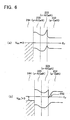
- FIG. 6 shows energy bands along the line VI-VI of FIG. 5 .
- the numbers shown in the energy bands correspond to the numbers of layers in the cross-sectional view of essential parts shown in FIG. 5 .
- FIG. 6 (a) shows a state where voltage is not being applied to the gate electrode 244, and FIG. 6 (b) shows a state where positive voltage is being applied to the gate electrode 244.
- a potential well 252 is generated while a positive voltage is applied to the gate electrode 244, and the energy level of a conduction band in the vicinity of the junction between the p-GaN layer 232 and the n-AlGaN layer 233 becomes below the Fermi level. Consequently, 2DEG is generated in the potential well 252.
- the 2DEG electrons move two dimensionally within the potential well 252, flowing between the drain electrode 242 and the source electrode 246.
- the semiconductor device 200 is thus turned on while the positive voltage is applied to the gate electrode 244.
- the n-AlGaN layer 233 and the p-AlGaN layer 235 are adjacent, and consequently the n-AlGaN layer 233 and the p-AlGaN layer 235 are depleted.
- the potential well formed by the p-GaN layer 232 and the n-AlGaN layer 233 is consequently above the Fermi level, and extremely stable normally-off operation is realized.
- n-AlGaN layer 233 and the p-AlGaN layer 235 fulfill the following relational expressions: Xd ⁇ 2 ⁇ Nd ⁇ Vd / qNa Na + Nd 1 / 2 Xa ⁇ 2 ⁇ Na ⁇ Vd / qNd Na + Nd 1 / 2
- Xd is thickness of the n-AlGaN layer 233
- Nd is donor density of the n-AlGaN layer 233
- Xa is thickness of the p-AlGaN layer 235
- Na is acceptor density of the p-AlGaN layer 235
- Vd is diffusion potential formed by the n-AlGaN layer 233 and the p-AlGaN layer 235
- ⁇ permittivity of the GaN semiconducting crystal
- q is absolute value of the electron charge.
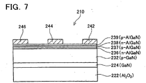
- FIG. 7 schematically shows a cross-sectional view of essential parts of a variant semiconductor device 210.
- Compositional elements identical with the third embodiment have the same reference numbers assigned thereto and a description thereof is omitted.
- the characteristic feature of the present variant can be understood clearly when compared with the semiconductor device 200 of FIG. 5 .
- the semiconductor device 210 there is a repetition of unit of layers equivalent to the n-AlGaN layer 233 (an example of a second layer) and the p-AlGaN layer 235 (an example of a surface layer) of the semiconductor device 200 of the third embodiment.
- the equivalents of the n-AlGaN layer 233 of the semiconductor device 200 are n-AlGaN layers 236 and 238 (examples of a second layer), and the equivalents of the p-AlGaN layer 235 are p-AlGaN layers 237 and 239 (upper layers).
- the semiconductor device 210 comprises the first n-AlGaN layer 236, the first p-AlGaN layer 237 stacked thereon, the second n-AlGaN layer 238 stacked thereon, and the second p-AlGaN layer 239 stacked thereon.
- the combination of the first n-AlGaN layer 236 and the first p-AlGaN layer 237 stacked thereon forms a first unit of layers.
- the combination of the second n-AlGaN layer 238 and the second p-AlGaN layer 239 stacked thereon forms a second unit of layers.
- the second unit of layers is stacked on the first unit of layers.
- a stacked structure of units of layers such as the semiconductor device 210, essentially hastens the depletion of the n-AlGaN layer 236 and the n-AlGaN layer 238, which are equivalent to electron supply layers. It is consequently easy to realize stable normally-off operation.
- Electron supply capacity can therefore increase, and on-resistance can be reduced.
- the manufacturing method of the semiconductor device of the embodiment of the invention can essentially be realized using the manufacturing technique described above.
Landscapes
- Junction Field-Effect Transistors (AREA)
Claims (8)
- Transistor, aufweisend:eine erste Schicht (232);eine zweite Schicht (233), die auf eine obere Oberfläche der ersten Schicht (232) gestapelt ist;eine Oberflächenschicht (235), die auf eine obere Oberfläche der zweiten Schicht (233) gestapelt ist; undeine Gate-Elektrode (244), die auf einer oberen Oberflächenseite der Oberflächenschicht (235) ausgebildet ist;wobei die erste Schicht (232) eine Galliumnitrid- (GaN-) Verbindung ist, die einen ersten III-V-Nitrid-Halbleiter aufweist,die zweite Schicht (233) eine Galliumnitrid- (GaN-) Verbindung ist, die einen zweiten III-V-Nitrid-Halbleiter mit einer Leitfähigkeit eines zweiten Typs eines p- oder n-Typs aufweist,die Oberflächenschicht (235) eine Galliumnitird- (GaN-) Verbindung ist, die einen III-V-Nitrid-Halbleiter mit einer Leitfähigkeit eines ersten Typs aufweist, die entgegengesetzt zur Leitfähigkeit des zweiten Typs ist, undeine Bandlücke des zweiten III-V-Nitrid-Halbleiters breiter ist als eine Bandlücke des ersten III-V-Nitrid-Halbleiters.
- Transistor nach Anspruch 1,
wobei der III-V-Nitrid-Halbleiter in der Oberflächenschicht (235) der zweite III-V-Nitrid-Halbleiter ist. - Transistor, aufweisend:eine erste Schicht (232);eine Mehrzahl von aus Schichten (236 und 237, 238 und 239) bestehenden Einheiten, wobei jede der aus Schichten (236 und 237, 238 und 239) bestehenden Einheiten eine zweite Schicht (236, 238) und eine obere Schicht (237, 239), die auf eine obere Oberfläche der zweiten Schicht (236, 238) gestapelt ist, aufweist, und jede der aus Schichten (238 und 239) bestehenden Einheiten auf eine obere Oberfläche einer unteren aus Schichten (236 und 237) bestehenden Einheit gestapelt ist; undeine Gate-Elektrode (244), die auf einer oberen Oberflächenseite der obersten aus Schichten (238 und 239) bestehenden Einheit ausgebildet ist;wobei die erste Schicht (232) eine Galliumnitrid- (GaN-) Verbindung ist, die einen ersten III-V-Nitrid-Halbleiter aufweist,die zweite Schicht (236, 238) eine Galliumnitrid- (GaN-) Verbindung ist, die einen zweiten III-V-Nitrid-Halbleiter mit einer Leit-fähigkeit eines zweiten Typs eines p- oder n-Typs aufweist,die obere Schicht (237, 239) eine Galliumnitrid- (GaN-) Verbindung ist, die einen III-V-Nitrid-Halbleiter mit einer Leitfähigkeit eines ersten Typs aufweist, die entgegengesetzt zur Leitfähigkeit des zweiten Typs ist, undeine Bandlücke des zweiten III-V-Nitrid-Halbleiters breiter ist als eine Bandlücke des ersten III-V-Nitrid-Halbleiters.
- Transistor nach Anspruch 3,
wobei der III-V-Nitrid-Halbleiter in der oberen Schicht (237, 239) der zweite III-V-Nitrid-Halbleiter ist. - Verfahren zum Herstellen eines Transistors mit einer ersten Schicht (232), einer zweiten Schicht (233), die auf eine obere Oberfläche der ersten Schicht (232) gestapelt ist, einer Oberflächenschicht (235), die auf eine obere Oberfläche der zweiten Schicht (233) gestapelt ist, und einer Gate-Elektrode (244), die auf einer oberen Oberflächenseite der Oberflächenschicht (235) ausgebildet ist, wobei das Verfahren umfasst:einen Schritt, in dem die zweite Schicht (233) auf der oberen Oberfläche der ersten Schicht (232) durch epitaxiales Wachstum aufgewachsen wird;einen Schritt, in dem die Oberflächenschicht (235) auf der oberen Oberfläche der zweiten Schicht (232) durch epitaxiales Wachstum aufgewachsen wird;einen Schritt, in dem die Gate-Elektrode (244) auf der oberen Oberflächenseite der Oberflächenschicht (235) ausgebildet wird;wobei die erste Schicht (232) eine Galliumnitrid- (GaN-) Verbindung ist, die einen ersten III-V-Halbleiter aufweist,die zweite Schicht (233) eine Galliumnitrid- (GaN-) Verbindung ist, die einen zweiten III-V-Nitrid-Halbleiter mit einer Leitfähigkeit eines zweiten Typs eines p- oder n-Typs aufweist,die Oberflächenschicht (235) eine Galliumnitrid- (GaN-) Verbindung ist, die einen III-V-Nitrid-Halbleiter mit einer Leitfähigkeit eines ersten Typs aufweist, die der entgegengesetzt zur Leitfähigkeit des zweiten Typs ist, undeine Bandlücke des zweiten III-V-Nitrid-Halbleiters breiter ist als eine Bandlücke des ersten III-V-Nitrid-Halbleiters.
- Verfahren zum Herstellen eines Transistors nach Anspruch 5,
wobei der III-V-Nitrid-Halbleiter in der Oberflächenschicht (235) der zweite III-V-Nitrid-Halbleiter ist. - Verfahren zum Herstellen eines Transistors mit einer ersten Schicht (232), einer Mehrzahl von aus Schichten (236 und 237, 238 und 239) bestehenden Einheiten und einer Gate-Elektrode (244), die auf einer oberen Oberflächenseite der obersten aus Schichten (238 und 239) bestehenden Einheit ausgebildet ist, wobei jede der aus Schichten (236 und 237, 238 und 239) bestehenden Einheiten eine zweite Schicht (236, 238) und eine obere Schicht (237, 239), die auf eine obere Oberfläche der zweiten Schicht (236, 238) gestapelt ist, aufweist, und jede der aus Schichten (238 und 239) bestehenden Einheiten auf eine obere Oberfläche einer unteren aus Schichten (236 und 237) bestehenden Einheit gestapelt ist, wobei das Verfahren umfasst:(a) einen Schritt, in dem die zweite Schicht (236) auf der oberen Oberfläche der ersten Schicht (232) durch epitaxiales Wachstum aufgewachsen wird;(b) einen Schritt, in dem die obere Schicht (237) auf einer oberen Oberfläche der zweiten Schicht (236) durch epitaxiales Wachstum aufgewachsen wird;(c) einen Schritt, in dem die zweite Schicht (238) auf einer oberen Oberfläche der oberen Schicht (237) durch epitaxiales Wachstum aufgewachsen wird;(d) einen Schritt, in dem die obere Schicht (239) auf einer oberen Oberfläche der zweiten Schicht (238) durch epitaxiales Wachstum aufgewachsen wird;(e) Wiederholen der Schritte (c) und (d) über einen vorgegebenen Zyklus; und(f) einen Schritt, in dem die Gate-Elektrode (244) auf einer oberen Oberflächenseite einer obersten oberen Schicht (239) ausgebildet wird;wobei die erste Schicht (232) eine Galliumnitrid- (GaN-) Verbindung ist, die einen ersten III-V-Nitrid-Halbleiter aufweist,
die zweite Schicht (236, 238) eine Galliumnitrid- (GaN-) Verbindung ist, die einen zweiten III-V-Nitrid-Halbleiter mit einer Leitfähigkeit eines zweiten Typs eines p- oder n-Typs aufweist,
die obere Schicht (237, 239) eine Galliumnitrid- (GaN-) Verbindung ist, die einen III-V-Nitrid-Halbleiter mit einer Leitfähigkeit eines Typs aufweist, die entgegengesetzt zur Leitfähigkeit des zweiten Typs ist, und
eine Bandlücke des zweiten III-V-Halbleiters breiter ist als eine Bandlücke des ersten III-V-Nitrid-Halbleiters. - Verfahren zum Herstellen eines Transistors nach Anspruch 7,
wobei der III-V-Nitrid-Halbleiter in der oberen Schicht (237, 239) der zweite III-V-Nitrid-Halbleiter ist.
Applications Claiming Priority (2)
| Application Number | Priority Date | Filing Date | Title |
|---|---|---|---|
| JP2004210989A JP4744109B2 (ja) | 2004-07-20 | 2004-07-20 | 半導体装置とその製造方法 |
| PCT/JP2005/011891 WO2006008925A1 (en) | 2004-07-20 | 2005-06-22 | Iii-v hemt devices |
Publications (4)
| Publication Number | Publication Date |
|---|---|
| EP1779438A1 EP1779438A1 (de) | 2007-05-02 |
| EP1779438B1 EP1779438B1 (de) | 2012-01-18 |
| EP1779438B8 EP1779438B8 (de) | 2012-03-21 |
| EP1779438B2 true EP1779438B2 (de) | 2019-07-31 |
Family
ID=34975181
Family Applications (1)
| Application Number | Title | Priority Date | Filing Date |
|---|---|---|---|
| EP05755884.3A Expired - Lifetime EP1779438B2 (de) | 2004-07-20 | 2005-06-22 | Iii-v-hemt-bauelemente |
Country Status (5)
| Country | Link |
|---|---|
| US (3) | US7777252B2 (de) |
| EP (1) | EP1779438B2 (de) |
| JP (1) | JP4744109B2 (de) |
| CN (1) | CN100530687C (de) |
| WO (1) | WO2006008925A1 (de) |
Families Citing this family (61)
| Publication number | Priority date | Publication date | Assignee | Title |
|---|---|---|---|---|
| JP4744109B2 (ja) | 2004-07-20 | 2011-08-10 | トヨタ自動車株式会社 | 半導体装置とその製造方法 |
| JP2007250727A (ja) * | 2006-03-15 | 2007-09-27 | Toyota Central Res & Dev Lab Inc | 電界効果トランジスタ |
| KR100714629B1 (ko) * | 2006-03-17 | 2007-05-07 | 삼성전기주식회사 | 질화물 반도체 단결정 기판, 그 제조방법 및 이를 이용한수직구조 질화물 발광소자 제조방법 |
| JP5400266B2 (ja) * | 2006-04-17 | 2014-01-29 | パナソニック株式会社 | 電界効果トランジスタ |
| JP4755961B2 (ja) | 2006-09-29 | 2011-08-24 | パナソニック株式会社 | 窒化物半導体装置及びその製造方法 |
| JP5186096B2 (ja) | 2006-10-12 | 2013-04-17 | パナソニック株式会社 | 窒化物半導体トランジスタ及びその製造方法 |
| DE112008000409T5 (de) * | 2007-02-16 | 2009-12-24 | Sumitomo Chemical Company, Limited | Epitaxiales Substrat für einen Feldeffekttransistor |
| JP5358901B2 (ja) * | 2007-06-19 | 2013-12-04 | 日本電気株式会社 | 半導体装置 |
| US8461626B2 (en) | 2007-07-09 | 2013-06-11 | Freescale Semiconductor, Inc. | Hetero-structure field effect transistor, integrated circuit including a hetero-structure field effect transistor and method for manufacturing a hetero-structure field effect transistor |
| JP5056272B2 (ja) * | 2007-08-28 | 2012-10-24 | 住友電気工業株式会社 | 窒化ガリウム系半導体面発光素子、および窒化ガリウム系半導体面発光素子を作製する方法 |
| US7915643B2 (en) | 2007-09-17 | 2011-03-29 | Transphorm Inc. | Enhancement mode gallium nitride power devices |
| JP4729067B2 (ja) * | 2008-03-31 | 2011-07-20 | 古河電気工業株式会社 | 電界効果トランジスタ |
| US8519438B2 (en) | 2008-04-23 | 2013-08-27 | Transphorm Inc. | Enhancement mode III-N HEMTs |
| US8289065B2 (en) | 2008-09-23 | 2012-10-16 | Transphorm Inc. | Inductive load power switching circuits |
| US7898004B2 (en) | 2008-12-10 | 2011-03-01 | Transphorm Inc. | Semiconductor heterostructure diodes |
| EP2202802B1 (de) * | 2008-12-24 | 2012-09-26 | Semiconductor Energy Laboratory Co., Ltd. | Treiberschaltung und Halbleiterbauelement |
| KR101666910B1 (ko) * | 2009-04-08 | 2016-10-17 | 이피션트 파워 컨버젼 코퍼레이션 | 증가형 GaN HEMT 장치 및 그 제조 방법 |
| JP5453892B2 (ja) * | 2009-04-15 | 2014-03-26 | トヨタ自動車株式会社 | 窒化物半導体装置 |
| US8742459B2 (en) | 2009-05-14 | 2014-06-03 | Transphorm Inc. | High voltage III-nitride semiconductor devices |
| JP5435459B2 (ja) * | 2009-05-20 | 2014-03-05 | 古河電気工業株式会社 | 電界効果トランジスタ |
| JP2011040676A (ja) * | 2009-08-18 | 2011-02-24 | Sanken Electric Co Ltd | 半導体装置及びその製造方法 |
| US8390000B2 (en) | 2009-08-28 | 2013-03-05 | Transphorm Inc. | Semiconductor devices with field plates |
| US8541817B2 (en) * | 2009-11-06 | 2013-09-24 | Nitek, Inc. | Multilayer barrier III-nitride transistor for high voltage electronics |
| US9825162B2 (en) | 2009-11-19 | 2017-11-21 | Nxp Usa, Inc. | Vertical power transistor device, semiconductor die and method of manufacturing a vertical power transistor device |
| US8389977B2 (en) | 2009-12-10 | 2013-03-05 | Transphorm Inc. | Reverse side engineered III-nitride devices |
| US20110204376A1 (en) * | 2010-02-23 | 2011-08-25 | Applied Materials, Inc. | Growth of multi-junction led film stacks with multi-chambered epitaxy system |
| JPWO2011118098A1 (ja) * | 2010-03-26 | 2013-07-04 | 日本電気株式会社 | 電界効果トランジスタ、電界効果トランジスタの製造方法、および電子装置 |
| JP2011210750A (ja) * | 2010-03-26 | 2011-10-20 | Nec Corp | 電界効果トランジスタ、電界効果トランジスタの製造方法、および電子装置 |
| JPWO2011118099A1 (ja) * | 2010-03-26 | 2013-07-04 | 日本電気株式会社 | 電界効果トランジスタ、電界効果トランジスタの製造方法、および電子装置 |
| TWI420664B (zh) * | 2010-07-27 | 2013-12-21 | 國立交通大學 | 增強式高電子移動率電晶體及其製造方法 |
| US9076827B2 (en) | 2010-09-14 | 2015-07-07 | Applied Materials, Inc. | Transfer chamber metrology for improved device yield |
| KR20120027988A (ko) | 2010-09-14 | 2012-03-22 | 삼성엘이디 주식회사 | 질화갈륨계 반도체소자 및 그 제조방법 |
| US8742460B2 (en) | 2010-12-15 | 2014-06-03 | Transphorm Inc. | Transistors with isolation regions |
| US8643062B2 (en) | 2011-02-02 | 2014-02-04 | Transphorm Inc. | III-N device structures and methods |
| ES2834617T3 (es) | 2011-02-17 | 2021-06-18 | Fujirebio Diagnostics Inc | Composiciones y métodos de uso para la determinación de HE4a |
| US8716141B2 (en) | 2011-03-04 | 2014-05-06 | Transphorm Inc. | Electrode configurations for semiconductor devices |
| US8772842B2 (en) | 2011-03-04 | 2014-07-08 | Transphorm, Inc. | Semiconductor diodes with low reverse bias currents |
| JP2011142358A (ja) * | 2011-04-22 | 2011-07-21 | Panasonic Corp | 窒化物半導体装置 |
| US8901604B2 (en) | 2011-09-06 | 2014-12-02 | Transphorm Inc. | Semiconductor devices with guard rings |
| US9257547B2 (en) | 2011-09-13 | 2016-02-09 | Transphorm Inc. | III-N device structures having a non-insulating substrate |
| JP5908692B2 (ja) * | 2011-09-29 | 2016-04-26 | トランスフォーム・ジャパン株式会社 | 化合物半導体装置及びその製造方法 |
| US8598937B2 (en) | 2011-10-07 | 2013-12-03 | Transphorm Inc. | High power semiconductor electronic components with increased reliability |
| US9165766B2 (en) | 2012-02-03 | 2015-10-20 | Transphorm Inc. | Buffer layer structures suited for III-nitride devices with foreign substrates |
| CN102637723A (zh) * | 2012-03-28 | 2012-08-15 | 华为技术有限公司 | GaN衬底、半导体器件及其制作方法 |
| WO2013155108A1 (en) | 2012-04-09 | 2013-10-17 | Transphorm Inc. | N-polar iii-nitride transistors |
| US9184275B2 (en) | 2012-06-27 | 2015-11-10 | Transphorm Inc. | Semiconductor devices with integrated hole collectors |
| US8803246B2 (en) | 2012-07-16 | 2014-08-12 | Transphorm Inc. | Semiconductor electronic components with integrated current limiters |
| US9171730B2 (en) | 2013-02-15 | 2015-10-27 | Transphorm Inc. | Electrodes for semiconductor devices and methods of forming the same |
| US9087718B2 (en) | 2013-03-13 | 2015-07-21 | Transphorm Inc. | Enhancement-mode III-nitride devices |
| US9245993B2 (en) | 2013-03-15 | 2016-01-26 | Transphorm Inc. | Carbon doping semiconductor devices |
| KR102071019B1 (ko) * | 2013-05-10 | 2020-01-29 | 서울반도체 주식회사 | 노멀리 오프 타입 트랜지스터 및 그 제조방법 |
| WO2015009514A1 (en) | 2013-07-19 | 2015-01-22 | Transphorm Inc. | Iii-nitride transistor including a p-type depleting layer |
| JP2015046444A (ja) * | 2013-08-27 | 2015-03-12 | ルネサスエレクトロニクス株式会社 | 半導体装置 |
| US9660067B2 (en) * | 2014-03-25 | 2017-05-23 | Intel Corporation | III-N transistors with epitaxial layers providing steep subthreshold swing |
| US9318593B2 (en) | 2014-07-21 | 2016-04-19 | Transphorm Inc. | Forming enhancement mode III-nitride devices |
| US9536966B2 (en) | 2014-12-16 | 2017-01-03 | Transphorm Inc. | Gate structures for III-N devices |
| US9536967B2 (en) | 2014-12-16 | 2017-01-03 | Transphorm Inc. | Recessed ohmic contacts in a III-N device |
| JP6685278B2 (ja) * | 2015-03-11 | 2020-04-22 | パナソニック株式会社 | 窒化物半導体装置 |
| JP6888013B2 (ja) | 2016-01-15 | 2021-06-16 | トランスフォーム テクノロジー,インコーポレーテッド | AL(1−x)Si(x)Oゲート絶縁体を有するエンハンスメントモードIII族窒化物デバイス |
| TWI813243B (zh) | 2016-05-31 | 2023-08-21 | 美商創世舫科技有限公司 | 包含漸變空乏層的三族氮化物裝置 |
| US20180061975A1 (en) * | 2016-08-24 | 2018-03-01 | Rohm Co., Ltd. | Nitride semiconductor device and nitride semiconductor package |
Citations (4)
| Publication number | Priority date | Publication date | Assignee | Title |
|---|---|---|---|---|
| US5949096A (en) † | 1997-09-29 | 1999-09-07 | Nec Corporation | Field effect transistor with stabilized threshold voltage |
| US20010015437A1 (en) † | 2000-01-25 | 2001-08-23 | Hirotatsu Ishii | GaN field-effect transistor, inverter device, and production processes therefor |
| US20020066908A1 (en) † | 2000-12-01 | 2002-06-06 | Smith Richard Peter | Aluminum gallium nitride/gallium nitride high electron mobility transistors having a gate contact on a gallium nitride based cap segment and methods of fabricating same |
| JP2003059946A (ja) † | 2001-08-14 | 2003-02-28 | Furukawa Electric Co Ltd:The | GaN系半導体装置 |
Family Cites Families (31)
| Publication number | Priority date | Publication date | Assignee | Title |
|---|---|---|---|---|
| US4663643A (en) | 1981-04-23 | 1987-05-05 | Fujitsu Limited | Semiconductor device and process for producing the same |
| JPS5891682A (ja) | 1981-11-27 | 1983-05-31 | Hitachi Ltd | 半導体装置 |
| JPH0624208B2 (ja) | 1982-07-29 | 1994-03-30 | 日本電気株式会社 | 半導体装置 |
| US4600932A (en) | 1984-10-12 | 1986-07-15 | Gte Laboratories Incorporated | Enhanced mobility buried channel transistor structure |
| JPH088350B2 (ja) * | 1985-04-08 | 1996-01-29 | 日本電気株式会社 | 半導体装置 |
| JPH0415929A (ja) | 1990-05-10 | 1992-01-21 | Fujitsu Ltd | 高電子移動度トランジスタ |
| JPH0547800A (ja) | 1991-08-13 | 1993-02-26 | Fujitsu Ltd | 半導体装置及びその製造方法 |
| JP3256643B2 (ja) | 1995-03-09 | 2002-02-12 | 日本電信電話株式会社 | 半導体装置 |
| JPH11261053A (ja) | 1998-03-09 | 1999-09-24 | Furukawa Electric Co Ltd:The | 高移動度トランジスタ |
| JP2000068498A (ja) | 1998-08-21 | 2000-03-03 | Nippon Telegr & Teleph Corp <Ntt> | 絶縁性窒化物膜およびそれを用いた半導体装置 |
| US6586781B2 (en) * | 2000-02-04 | 2003-07-01 | Cree Lighting Company | Group III nitride based FETs and HEMTs with reduced trapping and method for producing the same |
| JP2002057158A (ja) * | 2000-08-09 | 2002-02-22 | Sony Corp | 絶縁性窒化物層及びその形成方法、半導体装置及びその製造方法 |
| JP4220683B2 (ja) * | 2001-03-27 | 2009-02-04 | パナソニック株式会社 | 半導体装置 |
| WO2003071607A1 (en) * | 2002-02-21 | 2003-08-28 | The Furukawa Electric Co., Ltd. | GaN FIELD-EFFECT TRANSISTOR |
| US6888170B2 (en) * | 2002-03-15 | 2005-05-03 | Cornell Research Foundation, Inc. | Highly doped III-nitride semiconductors |
| US6914273B2 (en) * | 2002-08-26 | 2005-07-05 | University Of Florida Research Foundation, Inc. | GaN-type enhancement MOSFET using hetero structure |
| JP2004210989A (ja) | 2003-01-07 | 2004-07-29 | Fujitaka Creation:Kk | マイナスイオンを発生する布地プリント用インク及び布地プリント方法 |
| TWI230978B (en) * | 2003-01-17 | 2005-04-11 | Sanken Electric Co Ltd | Semiconductor device and the manufacturing method thereof |
| US6933544B2 (en) * | 2003-01-29 | 2005-08-23 | Kabushiki Kaisha Toshiba | Power semiconductor device |
| CN100388509C (zh) | 2003-01-29 | 2008-05-14 | 株式会社东芝 | 功率半导体器件 |
| JP4645034B2 (ja) * | 2003-02-06 | 2011-03-09 | 株式会社豊田中央研究所 | Iii族窒化物半導体を有する半導体素子 |
| JP2004273486A (ja) | 2003-03-05 | 2004-09-30 | Mitsubishi Electric Corp | 半導体装置およびその製造方法 |
| US6787826B1 (en) | 2003-03-14 | 2004-09-07 | Triquint Semiconductor, Inc. | Heterostructure field effect transistor |
| US6835969B1 (en) * | 2003-06-26 | 2004-12-28 | Raytheon Company | Split-channel high electron mobility transistor (HEMT) device |
| JP2005086171A (ja) * | 2003-09-11 | 2005-03-31 | Fujitsu Ltd | 半導体装置及びその製造方法 |
| US7382001B2 (en) * | 2004-01-23 | 2008-06-03 | International Rectifier Corporation | Enhancement mode III-nitride FET |
| US7465997B2 (en) * | 2004-02-12 | 2008-12-16 | International Rectifier Corporation | III-nitride bidirectional switch |
| JP4041075B2 (ja) | 2004-02-27 | 2008-01-30 | 株式会社東芝 | 半導体装置 |
| US7550783B2 (en) * | 2004-05-11 | 2009-06-23 | Cree, Inc. | Wide bandgap HEMTs with source connected field plates |
| JP4744109B2 (ja) | 2004-07-20 | 2011-08-10 | トヨタ自動車株式会社 | 半導体装置とその製造方法 |
| US7566918B2 (en) * | 2006-02-23 | 2009-07-28 | Cree, Inc. | Nitride based transistors for millimeter wave operation |
-
2004
- 2004-07-20 JP JP2004210989A patent/JP4744109B2/ja not_active Expired - Fee Related
-
2005
- 2005-06-22 US US11/632,665 patent/US7777252B2/en active Active
- 2005-06-22 EP EP05755884.3A patent/EP1779438B2/de not_active Expired - Lifetime
- 2005-06-22 CN CNB2005800241914A patent/CN100530687C/zh not_active Expired - Fee Related
- 2005-06-22 WO PCT/JP2005/011891 patent/WO2006008925A1/en not_active Ceased
-
2010
- 2010-06-24 US US12/822,328 patent/US9184271B2/en not_active Expired - Lifetime
-
2014
- 2014-02-27 US US14/192,245 patent/US9735260B2/en not_active Expired - Fee Related
Patent Citations (4)
| Publication number | Priority date | Publication date | Assignee | Title |
|---|---|---|---|---|
| US5949096A (en) † | 1997-09-29 | 1999-09-07 | Nec Corporation | Field effect transistor with stabilized threshold voltage |
| US20010015437A1 (en) † | 2000-01-25 | 2001-08-23 | Hirotatsu Ishii | GaN field-effect transistor, inverter device, and production processes therefor |
| US20020066908A1 (en) † | 2000-12-01 | 2002-06-06 | Smith Richard Peter | Aluminum gallium nitride/gallium nitride high electron mobility transistors having a gate contact on a gallium nitride based cap segment and methods of fabricating same |
| JP2003059946A (ja) † | 2001-08-14 | 2003-02-28 | Furukawa Electric Co Ltd:The | GaN系半導体装置 |
Non-Patent Citations (3)
| Title |
|---|
| AMBACHER, O.: "Growth and applications of group III-nitrides", JOURNAL OF PHYSICS D: APPLIED PHY, vol. 31, no. 20, 21 October 1998 (1998-10-21), pages 2653 - 2710, XP009117690 † |
| COFFIE R ET AL: "p-capped GaN-AlGaN-GaN high-electron mobility transistors (HEMTs)", IEEE ELECTRON DEVICE LETTERS, vol. 23, no. 10, 1 October 2002 (2002-10-01), pages 588 - 590, XP011424636 † |
| KAMECHE, M. ET AL: "Comparing High-Frequency Control Devices", MICROWAVES & RF, March 2003 (2003-03-01), pages 53 - 71 † |
Also Published As
| Publication number | Publication date |
|---|---|
| CN101027780A (zh) | 2007-08-29 |
| JP2006032749A (ja) | 2006-02-02 |
| US20080073652A1 (en) | 2008-03-27 |
| JP4744109B2 (ja) | 2011-08-10 |
| US20140175518A1 (en) | 2014-06-26 |
| EP1779438A1 (de) | 2007-05-02 |
| EP1779438B8 (de) | 2012-03-21 |
| US7777252B2 (en) | 2010-08-17 |
| US9184271B2 (en) | 2015-11-10 |
| WO2006008925A1 (en) | 2006-01-26 |
| CN100530687C (zh) | 2009-08-19 |
| US9735260B2 (en) | 2017-08-15 |
| EP1779438B1 (de) | 2012-01-18 |
| US20100295098A1 (en) | 2010-11-25 |
Similar Documents
| Publication | Publication Date | Title |
|---|---|---|
| EP1779438B1 (de) | Iii-v-hemt-bauelemente | |
| US8907349B2 (en) | Semiconductor device and method of manufacturing the same | |
| EP2394299B1 (de) | Halbleiterstruktur und verfahren zum herstellen einer halbleiterstruktur | |
| JP5469098B2 (ja) | 電界効果トランジスタ及びその製造方法 | |
| CN104704608B (zh) | 氮化物半导体结构物 | |
| US12176430B2 (en) | Semiconductor structure and semiconductor device | |
| US8330187B2 (en) | GaN-based field effect transistor | |
| WO2010109566A1 (ja) | 半導体装置及びその製造方法 | |
| US20110215424A1 (en) | Semiconductor device and manufacturing method thereof | |
| CN107743655A (zh) | 外延ⅲ族氮化物中的掺杂阻挡层 | |
| JP2009032713A (ja) | GaNをチャネル層とする窒化物半導体トランジスタ及びその作製方法 | |
| JP2010171416A (ja) | 半導体装置、半導体装置の製造方法および半導体装置のリーク電流低減方法 | |
| WO2003103037A1 (fr) | Dispositif a semi-conducteur | |
| JP2007080855A (ja) | 電界効果型トランジスタ | |
| KR100860070B1 (ko) | 트랜지스터 | |
| JP5221577B2 (ja) | 半導体装置とその製造方法 | |
| JP6096523B2 (ja) | 半導体装置とその製造方法 | |
| JP2006190988A (ja) | 半導体装置 | |
| US20260090001A1 (en) | Nitride-based semiconductor device and method for manufacturing thereof | |
| JP6185508B2 (ja) | 半導体装置とその製造方法 |
Legal Events
| Date | Code | Title | Description |
|---|---|---|---|
| PUAI | Public reference made under article 153(3) epc to a published international application that has entered the european phase |
Free format text: ORIGINAL CODE: 0009012 |
|
| 17P | Request for examination filed |
Effective date: 20070109 |
|
| AK | Designated contracting states |
Kind code of ref document: A1 Designated state(s): DE FR GB |
|
| DAX | Request for extension of the european patent (deleted) | ||
| RBV | Designated contracting states (corrected) |
Designated state(s): DE FR GB |
|
| 17Q | First examination report despatched |
Effective date: 20090929 |
|
| GRAP | Despatch of communication of intention to grant a patent |
Free format text: ORIGINAL CODE: EPIDOSNIGR1 |
|
| GRAS | Grant fee paid |
Free format text: ORIGINAL CODE: EPIDOSNIGR3 |
|
| GRAA | (expected) grant |
Free format text: ORIGINAL CODE: 0009210 |
|
| AK | Designated contracting states |
Kind code of ref document: B1 Designated state(s): DE FR GB |
|
| REG | Reference to a national code |
Ref country code: GB Ref legal event code: FG4D |
|
| RIN2 | Information on inventor provided after grant (corrected) |
Inventor name: SOEJIMA, NARUMASA;C/O K. K. TOYOTA CHUO KENKYUSHO Inventor name: UEDA, HIROYUKI;C/O K. K. TOYOTA CHUO KENKYUSHO Inventor name: SUGIMOTO, MASAHIRO;C/O TOYOTA JIDOSHA K. K. Inventor name: NAKANO, YOSHITAKA;C/O K. K. TOYOTA CHUO KENKYUSHO Inventor name: UESUGI, TSUTOMU;C/O K. K. TOYOTA CHUO KENKYUSHO Inventor name: KACHI, TETSU;C/O K. K. TOYOTA CHUO KEN KENKYUSHO |
|
| REG | Reference to a national code |
Ref country code: DE Ref legal event code: R096 Ref document number: 602005032282 Country of ref document: DE Effective date: 20120315 |
|
| RIN2 | Information on inventor provided after grant (corrected) |
Inventor name: KACHI, TETSU;C/O K. K. TOYOTA CHUO KENKYUSHO Inventor name: SUGIMOTO, MASAHIRO;C/O TOYOTA JIDOSHA K. K. Inventor name: SOEJIMA, NARUMASA;C/O K. K. TOYOTA CHUO KENKYUSHO Inventor name: UESUGI, TSUTOMU;C/O K. K. TOYOTA CHUO KENKYUSHO Inventor name: NAKANO, YOSHITAKA;C/O K. K. TOYOTA CHUO KENKYUSHO Inventor name: UEDA, HIROYUKI;C/O K. K. TOYOTA CHUO KENKYUSHO |
|
| PLBI | Opposition filed |
Free format text: ORIGINAL CODE: 0009260 |
|
| 26 | Opposition filed |
Opponent name: INFINEON TECHNOLOGIES AUSTRIA AG Effective date: 20121018 |
|
| PLAX | Notice of opposition and request to file observation + time limit sent |
Free format text: ORIGINAL CODE: EPIDOSNOBS2 |
|
| REG | Reference to a national code |
Ref country code: DE Ref legal event code: R026 Ref document number: 602005032282 Country of ref document: DE Effective date: 20121018 |
|
| RAP2 | Party data changed (patent owner data changed or rights of a patent transferred) |
Owner name: TOYOTA JIDOSHA KABUSHIKI KAISHA |
|
| GBPC | Gb: european patent ceased through non-payment of renewal fee |
Effective date: 20120622 |
|
| RIN2 | Information on inventor provided after grant (corrected) |
Inventor name: UEDA, HIROYUKI; C/O K. K. TOYOTA CHUO KENKYUSHO Inventor name: KACHI, TETSU; C/O K. K. TOYOTA CHUO KENKYUSHO Inventor name: SOEJIMA, NARUMASA; C/O K. K. TOYOTA CHUO KENKYUSHO Inventor name: UESUGI, TSUTOMU; C/O K. K. TOYOTA CHUO KENKYUSHO Inventor name: SUGIMOTO, MASAHIRO; C/O TOYOTA JIDOSHA KABUSHIKI K Inventor name: NAKANO, YOSHITAKA; C/O K. K. TOYOTA CHUO KENKYUSHO |
|
| REG | Reference to a national code |
Ref country code: FR Ref legal event code: ST Effective date: 20130228 |
|
| PLBB | Reply of patent proprietor to notice(s) of opposition received |
Free format text: ORIGINAL CODE: EPIDOSNOBS3 |
|
| PG25 | Lapsed in a contracting state [announced via postgrant information from national office to epo] |
Ref country code: GB Free format text: LAPSE BECAUSE OF NON-PAYMENT OF DUE FEES Effective date: 20120622 Ref country code: FR Free format text: LAPSE BECAUSE OF NON-PAYMENT OF DUE FEES Effective date: 20120702 |
|
| REG | Reference to a national code |
Ref country code: DE Ref legal event code: R084 Ref document number: 602005032282 Country of ref document: DE Effective date: 20130319 |
|
| APAH | Appeal reference modified |
Free format text: ORIGINAL CODE: EPIDOSCREFNO |
|
| APBM | Appeal reference recorded |
Free format text: ORIGINAL CODE: EPIDOSNREFNO |
|
| APBP | Date of receipt of notice of appeal recorded |
Free format text: ORIGINAL CODE: EPIDOSNNOA2O |
|
| APBQ | Date of receipt of statement of grounds of appeal recorded |
Free format text: ORIGINAL CODE: EPIDOSNNOA3O |
|
| RIN2 | Information on inventor provided after grant (corrected) |
Inventor name: UESUGI, TSUTOMU Inventor name: SOEJIMA, NARUMASA Inventor name: KACHI, TETSU Inventor name: NAKANO, YOSHITAKA Inventor name: SUGIMOTO, MASAHIRO Inventor name: UEDA, HIROYUKI |
|
| RIN2 | Information on inventor provided after grant (corrected) |
Inventor name: UESUGI, TSUTOMU Inventor name: KACHI, TETSU Inventor name: NAKANO, YOSHITAKA Inventor name: UEDA, HIROYUKI Inventor name: SOEJIMA, NARUMASA Inventor name: SUGIMOTO, MASAHIRO |
|
| PLAB | Opposition data, opponent's data or that of the opponent's representative modified |
Free format text: ORIGINAL CODE: 0009299OPPO |
|
| R26 | Opposition filed (corrected) |
Opponent name: INFINEON TECHNOLOGIES AUSTRIA AG Effective date: 20121018 |
|
| APBU | Appeal procedure closed |
Free format text: ORIGINAL CODE: EPIDOSNNOA9O |
|
| PUAH | Patent maintained in amended form |
Free format text: ORIGINAL CODE: 0009272 |
|
| STAA | Information on the status of an ep patent application or granted ep patent |
Free format text: STATUS: PATENT MAINTAINED AS AMENDED |
|
| 27A | Patent maintained in amended form |
Effective date: 20190731 |
|
| AK | Designated contracting states |
Kind code of ref document: B2 Designated state(s): DE FR GB |
|
| REG | Reference to a national code |
Ref country code: DE Ref legal event code: R102 Ref document number: 602005032282 Country of ref document: DE |
|
| REG | Reference to a national code |
Ref country code: DE Ref legal event code: R082 Ref document number: 602005032282 Country of ref document: DE Representative=s name: KUHNEN & WACKER PATENT- UND RECHTSANWALTSBUERO, DE Ref country code: DE Ref legal event code: R081 Ref document number: 602005032282 Country of ref document: DE Owner name: DENSO CORPORATION, KARIYA-CITY, JP Free format text: FORMER OWNER: TOYOTA JIDOSHA KABUSHIKI KAISHA, TOYOTA-SHI, AICHI-KEN, JP |
|
| PGFP | Annual fee paid to national office [announced via postgrant information from national office to epo] |
Ref country code: DE Payment date: 20220620 Year of fee payment: 18 |
|
| REG | Reference to a national code |
Ref country code: DE Ref legal event code: R119 Ref document number: 602005032282 Country of ref document: DE |
|
| PG25 | Lapsed in a contracting state [announced via postgrant information from national office to epo] |
Ref country code: DE Free format text: LAPSE BECAUSE OF NON-PAYMENT OF DUE FEES Effective date: 20240103 |