EP1770849A2 - Unité d'alimentation de puissance à découpage - Google Patents
Unité d'alimentation de puissance à découpage Download PDFInfo
- Publication number
- EP1770849A2 EP1770849A2 EP06020616A EP06020616A EP1770849A2 EP 1770849 A2 EP1770849 A2 EP 1770849A2 EP 06020616 A EP06020616 A EP 06020616A EP 06020616 A EP06020616 A EP 06020616A EP 1770849 A2 EP1770849 A2 EP 1770849A2
- Authority
- EP
- European Patent Office
- Prior art keywords
- winding group
- primary
- winding
- sub
- group
- Prior art date
- Legal status (The legal status is an assumption and is not a legal conclusion. Google has not performed a legal analysis and makes no representation as to the accuracy of the status listed.)
- Withdrawn
Links
- 230000004044 response Effects 0.000 claims abstract description 24
- 238000004804 winding Methods 0.000 claims description 1015
- 238000009499 grossing Methods 0.000 claims description 44
- 230000008878 coupling Effects 0.000 claims description 20
- 238000010168 coupling process Methods 0.000 claims description 20
- 238000005859 coupling reaction Methods 0.000 claims description 20
- 238000010438 heat treatment Methods 0.000 abstract description 11
- 230000000694 effects Effects 0.000 description 27
- 238000010586 diagram Methods 0.000 description 25
- 239000003990 capacitor Substances 0.000 description 18
- 230000003247 decreasing effect Effects 0.000 description 17
- 230000005284 excitation Effects 0.000 description 17
- 230000004048 modification Effects 0.000 description 16
- 238000012986 modification Methods 0.000 description 16
- 230000000052 comparative effect Effects 0.000 description 11
- 230000002238 attenuated effect Effects 0.000 description 9
- 101100112673 Rattus norvegicus Ccnd2 gene Proteins 0.000 description 5
- 229910044991 metal oxide Inorganic materials 0.000 description 2
- 150000004706 metal oxides Chemical class 0.000 description 2
- 230000004075 alteration Effects 0.000 description 1
- 230000002500 effect on skin Effects 0.000 description 1
- 230000005669 field effect Effects 0.000 description 1
- 230000003071 parasitic effect Effects 0.000 description 1
- 230000009467 reduction Effects 0.000 description 1
- 239000004065 semiconductor Substances 0.000 description 1
- 238000005549 size reduction Methods 0.000 description 1
- 239000000758 substrate Substances 0.000 description 1
- 230000001131 transforming effect Effects 0.000 description 1
Images


Classifications
-
- H—ELECTRICITY
- H02—GENERATION; CONVERSION OR DISTRIBUTION OF ELECTRIC POWER
- H02M—APPARATUS FOR CONVERSION BETWEEN AC AND AC, BETWEEN AC AND DC, OR BETWEEN DC AND DC, AND FOR USE WITH MAINS OR SIMILAR POWER SUPPLY SYSTEMS; CONVERSION OF DC OR AC INPUT POWER INTO SURGE OUTPUT POWER; CONTROL OR REGULATION THEREOF
- H02M3/00—Conversion of dc power input into dc power output
- H02M3/22—Conversion of dc power input into dc power output with intermediate conversion into ac
- H02M3/24—Conversion of dc power input into dc power output with intermediate conversion into ac by static converters
- H02M3/28—Conversion of dc power input into dc power output with intermediate conversion into ac by static converters using discharge tubes with control electrode or semiconductor devices with control electrode to produce the intermediate ac
- H02M3/325—Conversion of dc power input into dc power output with intermediate conversion into ac by static converters using discharge tubes with control electrode or semiconductor devices with control electrode to produce the intermediate ac using devices of a triode or a transistor type requiring continuous application of a control signal
- H02M3/335—Conversion of dc power input into dc power output with intermediate conversion into ac by static converters using discharge tubes with control electrode or semiconductor devices with control electrode to produce the intermediate ac using devices of a triode or a transistor type requiring continuous application of a control signal using semiconductor devices only
-
- H—ELECTRICITY
- H01—ELECTRIC ELEMENTS
- H01F—MAGNETS; INDUCTANCES; TRANSFORMERS; SELECTION OF MATERIALS FOR THEIR MAGNETIC PROPERTIES
- H01F30/00—Fixed transformers not covered by group H01F19/00
- H01F30/06—Fixed transformers not covered by group H01F19/00 characterised by the structure
- H01F30/10—Single-phase transformers
-
- H—ELECTRICITY
- H02—GENERATION; CONVERSION OR DISTRIBUTION OF ELECTRIC POWER
- H02M—APPARATUS FOR CONVERSION BETWEEN AC AND AC, BETWEEN AC AND DC, OR BETWEEN DC AND DC, AND FOR USE WITH MAINS OR SIMILAR POWER SUPPLY SYSTEMS; CONVERSION OF DC OR AC INPUT POWER INTO SURGE OUTPUT POWER; CONTROL OR REGULATION THEREOF
- H02M7/00—Conversion of ac power input into dc power output; Conversion of dc power input into ac power output
- H02M7/003—Constructional details, e.g. physical layout, assembly, wiring or busbar connections
-
- H—ELECTRICITY
- H01—ELECTRIC ELEMENTS
- H01F—MAGNETS; INDUCTANCES; TRANSFORMERS; SELECTION OF MATERIALS FOR THEIR MAGNETIC PROPERTIES
- H01F27/00—Details of transformers or inductances, in general
- H01F27/34—Special means for preventing or reducing unwanted electric or magnetic effects, e.g. no-load losses, reactive currents, harmonics, oscillations, leakage fields
- H01F2027/348—Preventing eddy currents
Definitions
- the present invention relates to a switching power supply unit transforming an input AC voltage obtained by switching an input DC voltage by a transformer, and outputting an output DC voltage obtained by rectifying and smoothing the transformed output AC voltage, and particularly relates to a switching power supply unit preferably applicable using high switching frequency.
- a switching element such as MOS-FET (Metal-Oxide Semiconductor Field-Effect Transistor) is used for the switching circuit for size reduction.
- MOS-FET Metal-Oxide Semiconductor Field-Effect Transistor
- the switching element performs switching operation at high frequency such as 100 kHz or more, therefore an input AC voltage obtained by the switching is a high-frequency voltage.
- AC resistance of the transformer is increased due to a skin effect or a proximity effect, consequently heating is caused, leading to reduction in efficiency.
- a first switching power supply unit of an embodiment of the invention includes a transformer having a primary-winding group and a secondary-winding group, a switching circuit performing switching operation to allow a current direction of the primary-winding group to be changed in a time-divisional manner, and a rectifier-and-smoother circuit rectifying and smoothing AC voltage induced on the secondary-winding group in response to operation of the switching circuit.
- the primary-winding group includes a first primary-winding group and a second primary-winding group connected in series to each other
- the secondary-winding group includes a first secondary-winding group and a second secondary-winding group connected to each other.
- the first secondary-winding group and the second secondary-winding group are driven in a time-divisional manner in phases opposite to each other in response to operation of the switching circuit.
- Magnetic coupling between the first primary-winding group and the secondary-winding group is relatively strong when the first secondary-winding group is driven, while it is relatively loose when the second secondary-winding group is driven.
- magnetic coupling between the second primary-winding group and the secondary-winding group is relatively loose when the first secondary-winding group is driven, while it is relatively strong when the second secondary-winding group is driven.
- group means that one or at least two windings exist (hereinafter, mentioned in the same way).
- strength of magnetic coupling of the first primary-winding group and the second primary-winding group to the secondary-winding group is changed in phases opposite to each other in a time-divisional manner. At that time, current direction is opposite to each other in principle of the transformer between the first primary-winding group or the second primary-winding group, and the secondary-winding group. Accordingly, AC resistance is decreased in a winding group being more strongly magnetically coupled with the secondary-winding group among the primary-winding group because influence of a proximity effect is reduced, compared with a case that winding groups having the same current direction are approximated to each other.
- AC resistance is increased due to the proximity effect in a winding group being more loosely magnetically coupled with the secondary-winding group among the primary-winding group, compared with the winding group being more strongly magnetically coupled with the secondary-winding group among the primary-winding group.
- a second switching power supply unit of the embodiment of the invention includes a transformer having a primary-winding group and a secondary-winding group, a switching circuit performing switching operation to allow a current direction of the primary-winding group to be changed in a time-divisional manner, and a rectifier-and-smoother circuit rectifying and smoothing AC voltage induced on the secondary-winding group in response to operation of the switching circuit.
- the primary-winding group includes a first primary-winding group and a second primary-winding group connected in series to each other
- the secondary-winding group includes a first secondary-winding group and a second secondary-winding group connected to each other.
- the first primary-winding group is disposed near the first secondary-winding group rather than the second secondary-winding group
- the second primary-winding group is disposed near the second secondary-winding group rather than the first secondary-winding group.
- the rectifier-and-smoother circuit has a first rectifier element and a second rectifier element, the first and second rectifier elements being connected to the secondary-winding group to allow the first secondary-winding group and the second secondary-winding group to be driven in a time-divisional manner in phases opposite to each other in response to operation of the switching circuit.
- each of the first secondary-winding group, second secondary-winding group, first primary-winding group, and second primary-winding group may be configured by being wound in a cylindrical surface parallel to an extending direction of the center pillar, or wound in a plane perpendicular to the extending direction of the center pillar.
- respective windings of the primary-winding group and respective windings of the secondary-winding group are alternately stacked, and more preferably, they are stacked vertically symmetrically in a stacking direction.
- first secondary-winding group, first primary-winding group, second secondary-winding group, and second primary-winding group are preferably stacked in that order, and more preferably the first secondary-winding group, first primary-winding group, second primary-winding group, and second secondary-winding group are stacked in that order.
- the first secondary-winding group and the second secondary-winding group are driven in a time-divisional manner in phases opposite to each other in response to operation of the switching circuit.
- the first primary-winding group is disposed near the first secondary-winding group rather than the second secondary-winding group
- the second primary-winding group is disposed near the second secondary-winding group rather than the first secondary-winding group.
- the first primary-winding group is disposed near the first secondary-winding group rather than the second secondary-winding group, it is more strongly magnetically coupled with the secondary-winding group when the first secondary-winding group is driven, and it is more loosely magnetically coupled with the secondary-winding group when the second secondary-winding group is driven.
- the second primary-winding group is disposed near the second secondary-winding group rather than the first secondary-winding group, it is more strongly magnetically coupled with the secondary-winding group when the second secondary-winding group is driven, and it is more loosely magnetically coupled with the secondary-winding group when the first secondary-winding group is driven.
- current direction is opposite to each other in principle of the transformer between the first primary-winding group or the second primary-winding group, and the secondary-winding group. Accordingly, AC resistance is decreased in a winding group being more strongly magnetically coupled with the secondary-winding group among the primary-winding group because influence of a proximity effect is reduced, compared with a case that winding groups having the same current direction are approximated to each other. On the other hand, AC resistance is increased due to the proximity effect in a winding group being more loosely magnetically coupled with the secondary-winding group among the primary-winding group, compared with the winding group being more strongly magnetically coupled with the secondary-winding group among the primary-winding group.
- a third switching power supply unit of the embodiment of the invention includes: a transformer having a primary-winding group including a first primary-winding group and a second primary-winding group connected to each other, and a secondary-winding group including a first secondary-winding group and a second secondary-winding group connected to each other; a switching circuit performing switching operation to allow the first primary-winding group and the second primary-winding group to be driven in a time-divisional manner in phases opposite to each other; and a rectifier-and-smoother circuit rectifying and smoothing AC voltage induced on the secondary-winding group in response to operation of the switching circuit.
- the first primary-winding group includes a first primary-sub-winding group and a second primary-sub-winding group connected in series to each other, magnetic coupling between the first primary-sub-winding group and the secondary-winding group being relatively strong when the first secondary-winding group is driven, while magnetic coupling between the second primary-sub-winding group and the secondary-winding group being relatively loose when the first secondary-winding group is driven.
- the second primary-winding group includes a third primary-sub-winding group and a fourth primary-sub-winding group connected in series to each other, magnetic coupling between the third primary-sub-winding group and the secondary-winding group being relatively strong when the second secondary-winding group is driven, while magnetic coupling between the fourth primary-sub-winding group and the secondary-winding group being relatively loose when the second secondary-winding group is driven.
- the first primary-winding group and the second primary-winding group are driven in phases opposite to each other in a time-divisional manner in response to operation of the switching circuit.
- a portion where magnetic coupling with the secondary-winding group is strong first primary-sub-winding group
- a portion where magnetic coupling with the secondary-winding group is loose second primary-sub-winding group
- the second primary-winding group a portion where magnetic coupling with the secondary-winding group is strong (third primary-sub-winding group) and a portion where magnetic coupling with the secondary-winding group is loose (fourth primary-sub-winding group) are formed.
- AC resistance is decreased in the third primary-sub-winding group because influence of the proximity effect is reduced, compared with a case that winding groups having the same current direction are approximated to each other.
- AC resistance is increased due to the proximity effect in the fourth primary-winding group, compared with the third primary-sub-winding group.
- a fourth switching power supply unit of the embodiment of the invention includes: a transformer having a primary-winding group including a first primary-winding group and a second primary-winding group connected to each other, and a secondary-winding group including a first secondary-winding group and a second secondary-winding group connected to each other; a switching circuit performing switching operation to allow the first primary-winding group and the second primary-winding group to be driven in a time-divisional manner in phases opposite to each other; and a rectifier-and-smoother circuit rectifying and smoothing AC voltage induced on the secondary-winding group in response to operation of the switching circuit.
- the first primary-winding group includes a first primary-sub-winding group and a second primary-sub-winding group connected in series to each other, the first primary-sub-winding group being disposed near the first secondary-winding group rather than the second secondary-winding group, and the second primary-sub-winding group being disposed near the second secondary-winding group rather than the first secondary-winding group.
- the second primary-winding group includes a third primary-sub-winding group and a fourth primary-sub-winding group connected in series to each other, the third primary-sub-winding group being disposed near the second secondary-winding group rather than the first secondary-winding group, and the fourth primary-sub-winding group being disposed near the first secondary-winding group rather than the second secondary-winding group.
- the rectifier-and-smoother circuit has a first rectifier element and a second rectifier element connected to the secondary-winding group to allow the first secondary-winding group and the second secondary-winding group to be driven in a time-divisional manner in phases opposite to each other in response to operation of the switching circuit.
- first primary-sub-winding group, second primary-sub-winding group, third primary-sub-winding group, fourth primary-sub-winding group, first secondary-winding group, and second secondary-winding group may be configured by being wound in a cylindrical surface parallel to an extending direction of the center pillar, or wound in a plane perpendicular to the extending direction of the center pillar.
- respective windings of the primary-winding group and respective windings of the secondary-winding group are alternately stacked, and more preferably, they are stacked vertically symmetrically in a stacking direction.
- first secondary-winding group, first primary-winding group, second secondary-winding group, and second primary-winding group are preferably stacked in that order, and more preferably the first secondary-winding group, first primary-winding group, second primary-winding group, and second secondary-winding group are stacked in that order.
- the first secondary-winding group and the second secondary-winding group are driven in a time-divisional manner in phases opposite to each other in response to operation of the switching circuit.
- the first primary-sub-winding group and the fourth primary-sub-winding group are disposed near the first secondary-winding group rather than the second secondary-winding group, they are more strongly magnetically coupled with the secondary-winding group when the first secondary-winding group is driven, but more loosely magnetically coupled with the secondary-winding group when the second secondary-winding group is driven.
- the second primary-sub-winding group and the third primary-sub-winding group are disposed near the second secondary-winding group rather than the first secondary-winding group, they are more strongly magnetically coupled with the secondary-winding group when the second secondary-winding group is driven, but more loosely magnetically coupled with the secondary-winding group when the first secondary-winding group is driven.
- current direction is opposite to each other in principle of the transformer between the primary-winding group and the secondary-winding group. Accordingly, AC resistance is decreased in the first primary-sub-winding group because influence of a proximity effect is reduced, compared with a case that winding groups having the same current direction are approximated to each other.
- AC resistance is increased due to the proximity effect in the second primary-sub-winding group, compared with the first primary-sub-winding group.
- AC resistance is decreased in the third primary-sub-winding group because influence of the proximity effect is reduced, compared with the case that winding groups having the same current direction are approximated to each other.
- AC resistance is increased due to the proximity effect in the fourth primary-sub-winding group, compared with the third primary-sub-winding group.
- the first and second switching power supply unit of the embodiment of the invention since the first primary-winding group and the second primary-winding group, which have different strength of magnetic coupling with the secondary-winding group from each other, are connected in series to each other, ringing generated in an output AC voltage of the transformer is attenuated by AC resistance of a winding group having higher AC resistance among the primary-winding group. Thus, core loss in the transformer or a value of heating due to AC resistance of the transformer is decreased, consequently efficiency is improved.
- the third and fourth switching power supply unit of the embodiment of the invention since the first primary-sub-winding group and the second primary-sub-winding group, which have different strength of magnetic coupling with the secondary-winding group from each other, are connected in series to each other, and the third primary-sub-winding group and the fourth primary-sub-winding group, which have different strength of magnetic coupling with the secondary-winding group from each other, are connected in series to each other, ringing generated in an output AC voltage of the transformer is attenuated by AC resistance of a winding group having higher AC resistance among the primary-winding group.
- core loss in the transformer or a value of heating due to AC resistance of the transformer is decreased, consequently efficiency is improved.
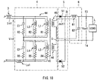
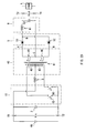
- Fig. 1 shows a circuit configuration of a switching power supply unit according to a first embodiment of the invention.
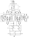
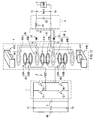
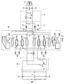
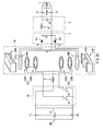
- Fig. 2 shows a structure of a transformer in the switching power supply unit of Fig. 1 in an exploded manner.
- the switching power supply unit acts as a DC-to-DC converter converting a high DC input voltage Vin supplied from a high-voltage battery HB into a lower DC output voltage Vout, and supplying the DC output voltage to a load L, and is a switching power supply unit of which the secondary side is in a center tap type.
- the switching power supply unit has an inverter circuit 1 (switching circuit) and a smoothing capacitor 2 provided between a primary-side high-voltage line L1H and a primary-side low-voltage line L1L; a transformer 4 configured to include a primary winding 44 including a primary winding 42 and a primary winding 43 connected in series to each other and a secondary winding 47 including a secondary winding 45 and a secondary winding 46 connected in series to each other; and a resonance inductor 3 provided between the inverter circuit 1 and the transformer 4.
- An input terminal T1 is provided in the primary-side high-voltage line L1H and an input terminal T2 is provided in the primary-side low-voltage line L1L, respectively, and the input terminals T1 and T2 are connected to output terminals of a high-voltage battery.
- the switching power supply unit has a rectifier circuit 5 and a smoothing circuit 6 provided in the secondary side of the transformer 4.
- An output terminal T3 is provided in an output line L0 as a line at high voltage side of the smoothing circuit 6, and an output terminal T4 is provided in a ground line LG as a line at low voltage side of the smoothing circuit 6, and the output terminals T3 and T4 are connected to input and output terminals of a load.
- a circuit including the rectifier circuit 5 and the smoothing circuit 6 corresponds to an example of the "rectifier-and-smoothing circuit" of the invention.
- the inverter circuit 1 is a single-phase inverter circuit converting the DC input voltage Vin outputted from the high-voltage battery into a single-phase AC voltage having an approximately rectangular wave shape.
- the inverter circuit 1 is a switching circuit in a full bridge type configured by full bridge connection of four switching elements 11, 12, 13 and 14 each of which is driven by a switching signal supplied from a control circuit (not shown).
- a control circuit not shown.
- MOS-FET Metal Oxide Semiconductor-Field Effect transistor
- IGBT Insulated Gate Bipolar Transistor
- the switching element 11 is provided between one end of the resonance inductor 3 and the primary-side high-voltage line L1H, and the switching element 12 is provided between one end of the resonance inductor 3 and the primary-side low-voltage line L1L.
- the switching element 13 is provided between one end of the primary wiring 43 of the transformer 4 and the primary-side high-voltage line L1H, and the switching element 14 is provided between one end of the primary wiring 43 and the primary-side low-voltage line L1L.
- in the inverter circuit 1 in response to operation of the switching elements 11 and 14, current flows along a first current path from the primary-side high-voltage line L1H to the primary-side low-voltage line L1L through the switching element 11, resonance inductor 3, primary winding 42 and switching element 14 in this order.
- the resonance inductor 3 configures a resonance circuit in cooperation with parasitic capacitance of at least one of switching elements 11, 12, 13 and 14, and reduces power loss caused by on/off of the respective switching elements by using a resonance characteristic of the resonance circuit. While the resonance inductor 3 may be configured by actually disposing a coil component, it may be configured by using series inductance including leakage inductance of the transformer 4 or wiring in place of (in cooperation with) this.
- the transformer 4 is a magnetic element having a primary winding 44 (primary-winding group) including a primary winding 42 (first primary-winding group) and a primary winding 43 (second primary-winding group) connected in series to each other, and a secondary winding 47 (secondary-winding group) including a secondary winding 45 (first secondary-winding group) and a secondary winding 46 (second secondary-winding group) connected in series to each other, the primary and the secondary windings 44 and 47 being magnetically coupled with each other by being wound on a magnetic core 41 to have polarity in the same direction.
- the transformer 4 is a stepdown type transformer, in which the number of turns of each of the secondary winding 45 and the secondary winding 46 is smaller than that of the primary winding 44.
- a stepdown level is determined by a ratio between the number of turns of the primary winding 44, and the number of turns of each of the secondary winding 45 and the secondary winding 46.
- the magnetic core 41 has a figure-of-eight magnetic path, and for example, includes a magnetic core 41A and a magnetic core 41B in an E-shape, respectively, and is configured by setting the magnetic core 41A on a conductive substrate (not shown) and superposing the magnetic core 41B on the magnetic core 41A.
- the magnetic core 41B is superposed on the magnetic core 41A, thereby a cylindrical center pillar 41C is formed in a central portion of the magnetic core 41.
- the center pillar 41C is for winding the primary winding 44, secondary winding 45, and secondary winding 46 of the transformer 4.
- the secondary winding 45 has a secondary winding 45A (first secondary-sub-winding group) and a secondary winding 45B (second secondary-sub-winding group) connected in parallel to each other
- the secondary winding 46 has a secondary winding 46A (third secondary-sub-winding group) and a secondary winding 46B (fourth secondary-sub-winding group) connected in parallel to each other.
- the secondary winding 45A, secondary winding 45B, secondary winding 46A, and secondary winding 46B are wound in one turn on the center pillar 41C in a plane perpendicular to an extending direction of the center pillar 41C, and layered in that order from above.
- One end of the secondary winding 45 is connected to an anode of a diode 51 described later, and the other end of the secondary winding 45 is connected to a center tap C, respectively.
- One end of the secondary winding 46 is connected to an anode of a diode 52 described later, and the other end of the secondary winding 46 is connected to the center tap C, respectively.
- the center tap C is connected to the output terminal T4 via a ground line LG. That is, the secondary side of the transformer 4 is in a center tap type connection.
- the secondary winding 45 and the secondary winding 46 are driven in phases opposite to each other in a time-divisional manner by the rectifier circuit 5, as described later.
- the primary winding 42 has a primary winding 42A (first primary-sub-winding group) and a primary winding 42B (second primary-sub-winding group) connected in series to each other.
- the primary winding 42A and the primary winding 42B are wound in three turns on the center pillar 41C in the plane perpendicular to the extending direction of the center pillar 41C, and layered in that order from above.
- the primary winding 42 is sandwiched by the secondary winding 45A and the secondary winding 45B, and the primary winding 42A is disposed close to the secondary winding 45A, and the primary winding 42B is disposed close to the secondary winding 45B. Accordingly, the primary winding 42 is disposed near the secondary winding 45 rather than the secondary winding 46.
- the primary winding 43 has a primary winding 43A (third primary-sub-winding group) and a primary winding 43B (fourth primary-sub-winding group) connected in series to each other.
- the primary winding 43A and the primary winding 43B are wound in three turns on the center pillar 41C in the plane perpendicular to the extending direction of the center pillar 41C, and layered in that order from above.
- the primary winding 43 is sandwiched by the secondary winding 46A and the secondary winding 46B, and the primary winding 43A is disposed adjacently to the secondary winding 46A, and the primary winding 43B is disposed adjacently to the secondary winding 46B. Accordingly, the primary winding 43 is disposed near the secondary winding 46 rather than the secondary winding 45.
- the transformer 4 has a structure where the primary winding (primary windings 42 and 43) and the secondary winding (secondary windings 45 and 46) are stacked in an alternate (sandwiched) manner, in which the primary winding 42 and the primary winding 43 having the same current direction are not close to each other.
- respective windings of the transformer 4 are disposed by stacking the secondary winding 45A (first secondary-sub-winding group), primary winding 42A (first primary-sub-winding group), primary winding 42B (second primary-sub-winding group), secondary winding 45B (second secondary-sub-winding group), secondary winding 46A (third secondary-sub-winding group), primary winding 43A (third primary-sub-winding group), primary winding 43B (fourth primary-sub-winding group), and secondary winding 46B (fourth secondary-sub-winding group) in this order from above. That is, a stacking structure of the transformer 4 is vertically symmetrical.
- Each of the primary winding 42 and the primary winding 43 are connected to the inverter circuit 1 to allow a direction of current flowing into the winding itself to be changed in response to operation of the inverter circuit 1.
- one end of the primary winding 42 is connected to a connection point between the switching element 11 and the switching element 12 via the resonance inductor 3, and the other end of the primary winding 42 is connected to one end of the primary winding 43, and the other end of the primary winding 43 is connected to a connection point between the switching element 13 and the switching element 14.
- the primary winding 42A, primary winding 42B, primary winding 43A, primary winding 43B, secondary winding 45A, secondary winding 45B, secondary winding 46A, and secondary winding 46B may be insulated from one another by air, or insulated from one another by interposing a not-shown insulating sheet.
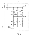
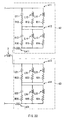
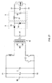
- the primary winding that is, the primary winding 44 including the primary winding 42 and the primary winding 43 can be expressed by an equivalent circuit as shown in Fig. 3. That is, the equivalent circuit is formed by a circuit a1, a circuit a2, and inductance Le1 connected in series to one another.
- the circuit a1 is configured by inductance L1 and resistance R1 connected in series to each other, inductance L2 and resistance R2 connected in series to each other, and line capacitance C1 and resistance R3 connected in series to each other, which are connected in parallel to one another.
- the circuit a2 is configured by connecting inductance L3 and resistance R4 connected in series to each other, inductance L4 and resistance R5 connected in series to each other, and line capacitance C2 and resistance R6 connected in series to each other, which are connected in parallel to one another.
- the inductance L1 is inductance of the primary winding 42 when the transformer 4 is assumed as an ideal transformer
- the resistance R1 is resistance of the primary winding 42 when the transformer 4 is assumed as an ideal transformer
- the inductance L2 is excitation inductance of the primary winding 42
- the resistance R2 is an AC resistance component of the primary winding 42.
- the line capacitance C1 is total capacitance of line capacitance in the primary winding 42 and line capacitance of the primary winding 42 and secondary windings 45 and 46; and the resistance R3 is an AC resistance component of the primary winding 42.
- the inductance L3 is inductance of the primary winding 43 when the transformer 4 is assumed as an ideal transformer, and the resistance R4 is resistance of the primary winding 43 when the transformer 4 is assumed as an ideal transformer.
- the inductance L4 is excitation inductance of the primary winding 43, and the resistance R5 is an AC resistance component of the primary winding 43.
- the line capacitance C2 is total capacitance of line capacitance in the primary winding 43 and line capacitance of the primary winding 43 and the secondary windings 45 and 46; and the resistance R6 is an AC resistance component of the primary winding 43.
- the inductance Le1 is leakage inductance of the transformer 4.
- the rectifier circuit 5 is in a single-phase full-wave rectification type including a pair of diodes of a diode 51 (first rectifier element) and a diode 52 (second rectifier element).
- An anode of the diode 51 is connected to one end of the secondary winding 45, and a cathode of the diode 51 is connected to a connection point D, respectively.
- An anode of the diode 52 is connected to one end of the secondary winding 46, and a cathode of the diode 52 is connected to the connection point D, respectively.
- the connection point D is connected to an output terminal T3 via the smoothing circuit 6.
- the smoothing circuit 6 includes a chalk coil 61 and a smoothing capacitor 62, and produces a DC output voltage Vout by smoothing a DC voltage rectified by the rectifier circuit 5, and then supplies the voltage Vout to a load L from the output terminals T3 and T4.
- the inverter circuit 1 is driven by typical switching operation is described below, the inverter circuit 1 may be driven by, for example, Zero Volt Switching operation.
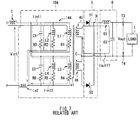
- the switching power supply unit transforms (steps down) a DC input voltage Vin supplied from a high-voltage battery into a DC output voltage Vout, and feeds the transformed DC output voltage Vout to a low-voltage buttery.
- a primary winding 144 of a transformer 104 includes a primary winding 142 and a primary winding 143 connected in parallel to each other as shown in Figs. 4 and 5, and in this point, the comparative example is different from the primary winding 44 of the embodiment.
- the primary winding 142 of the comparative example has a primary winding 142A and a primary winding 142B connected in series to each other, as the primary winding 42 of the embodiment.
- the primary winding 142A and the primary winding 142B are wound in six turns on the center pillar 41C in the plane perpendicular to the extending direction of the center pillar 41C, and layered in that order from above.
- the number of turns of the primary winding 142 is made twice the number of turns of the primary winding 42, that is, to be twelve turns.
- the primary winding 142 is sandwiched by a secondary winding 45A and a secondary winding 45B, and the primary winding 142A is disposed close to the secondary winding 45A, and the primary winding 142B is disposed close to the secondary winding 45B. Accordingly, the primary winding 142 is disposed near the secondary winding 45 rather than the secondary winding 46.
- the primary winding 143 of the comparative example has a primary winding 143A and a primary winding 143B connected in series to each other.
- the primary winding 143A and the primary winding 143B are wound in six turns on the center pillar 41C in the plane perpendicular to the extending direction of the center pillar 41C, and layered in that order from above.
- the number of turns of the primary winding 143 is made twice the number of turns of the primary winding 43, that is, to be twelve turns.
- the primary winding 143 is sandwiched by a secondary winding 46A and a secondary winding 46B, and the primary winding 143A is disposed adjacently to the secondary winding 46A, and the primary winding 142B is disposed adjacently to the secondary winding 46B. Accordingly, the primary winding 143 is disposed near the secondary winding 46 rather than the secondary winding 45.
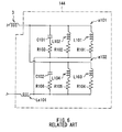
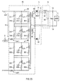
- the primary winding of the transformer 104 of the comparative example that is, the primary winding 144 including the primary winding 142 and the primary winding 143 can be expressed by an equivalent circuit as shown in Fig. 6. That is, the equivalent circuit is formed by a circuit including a circuit a101 and a circuit a102 connected in parallel to each other and inductance Le101, the circuit and the inductance Le101 being connected in series to each other.
- the circuit a101 is configured by inductance L101 and resistance R101 connected in series to each other, inductance L102 and resistance R102 connected in series to each other, and line capacitance C101 and resistance R103 connected in series to each other, which are connected in parallel to one another.
- the circuit a102 is configured by inductance L103 and resistance R104 connected in series to each other, inductance L104 and resistance R105 connected in series to each other, and line capacitance C102 and resistance R106 connected in series to each other, which are connected in parallel to one another.
- the inductance L101 is inductance of the primary winding 142 when the transformer 104 is assumed as an ideal transformer
- the resistance R101 is resistance of the primary winding 142 when the transformer 104 is assumed as an ideal transformer
- the inductance L102 is excitation inductance of the primary winding 142
- the resistance R102 is an AC resistance component of the primary winding 142.
- the line capacitance C101 is total capacitance of line capacitance in the primary winding 142 and line capacitance of the primary winding 142 and secondary windings 145 and 146; and the resistance R103 is an AC resistance component of the primary winding 142.
- the inductance L103 is inductance of the primary winding 143 when the transformer 104 is assumed as an ideal transformer, and the resistance R104 is resistance of the primary winding 143 when the transformer 40 is assumed as an ideal transformer.
- the inductance L104 is excitation inductance of the primary winding 143, and the resistance R105 is an AC resistance component of the primary winding 143.
- the line capacitance C102 is total capacitance of line capacitance in the primary winding 143 and line capacitance of the primary winding 143 and the secondary windings 145 and 146; and the resistance R106 is an AC resistance component of the primary winding 143.
- the inductance Le101 is leakage inductance of the transformer 104.
- the primary winding 143 since the primary winding 143 is disposed far from the secondary winding 45 into which current is flowing, it loosely magnetically coupled with the secondary winding 45. At that time, since the primary winding 143 is disposed relatively near to the secondary winding 46 into which current is not flowing, AC resistance is increased in the primary winding 143 due to the proximity effect, compared with the primary winding 142. Accordingly, only a relatively small current flows into the primary winding 143.
- the primary winding 142 is disposed far from the secondary winding 46 into which current is flowing, it loosely magnetically coupled with the secondary winding 46. At that time, since the primary winding 142 is disposed relatively near the secondary winding 45 into which current is not flowing, AC resistance is increased in the primary winding 142 due to the proximity effect, compared with the primary winding 143. Accordingly, only a relatively small current flows into the primary winding 142.
- the primary winding 43 is disposed far from the secondary winding 45 into which current is flowing, it magnetically coupled with the secondary winding 45 relatively loosely. At that time, since the primary winding 43 is disposed nearer to the secondary winding 46 into which current is not flowing, AC resistance is increased in the primary winding 43 due to the proximity effect, compared with the primary winding 42. However, since the primary winding 42 and the primary winding 43 are connected in series to each other in the embodiment, the same current flows into each of the primary winding 42 and the primary winding 43.
- the primary winding 42 is disposed far from the secondary winding 46 into which current is flowing, it magnetically coupled with the secondary winding 46 relatively loosely. At that time, since the primary winding 42 is disposed nearer to the secondary winding 45 into which current is not flowing, AC resistance is increased in the primary winding 42 due to the proximity effect, compared with the primary winding 43. However, since the primary winding 42 and the primary winding 43 are connected in series to each other in the embodiment, the same current flows into each of the primary winding 42 and the primary winding 43.
- a magnitude of AC resistance of the transformer 4 is not substantially different between a case that the secondary winding 45 is driven, and a case that the secondary winding 46 is driven. Accordingly, since an attenuation level of ringing is not substantially different between an output AC voltage when the secondary winding 45 is driven and an output AC voltage when the secondary winding 46 is driven, a heating level is not periodically increased, consequently high efficiency can be kept.
- a third primary winding 47 formed by stacking a third primary winding 47A and a third primary winding 47B in that order from above may be disposed between the secondary winding 45B and the secondary winding 46A while vertically symmetric arrangement is kept, as shown in Fig. 12.
- the secondary winding 45B and the secondary winding 46A may be omitted while vertically symmetric arrangement is kept as shown in Fig.
- the secondary winding 45A and the secondary winding 46B may be omitted as shown in Fig. 14. While vertically symmetric arrangement is not given, the secondary winding 45B and the secondary winding 46B may be omitted as shown in Fig. 15. In each case, it is enough that large AC resistance is disposed in series in the primary winding 44.
- respective windings of the transformer 4 is wound on the center pillar 41C in the plane perpendicular to the extending direction of the center pillar 41C in the embodiment, they may be wound on the center pillar 41C in a cylindrical surface parallel to the extending direction of the center pillar 41C, as shown in Figs. 16 to 19.
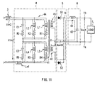
- Fig. 20 shows a circuit configuration of a switching power supply unit according to a second embodiment of the invention.
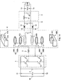
- Fig. 21 shows a structure of a transformer in the switching power supply unit of Fig. 20 in an exploded manner.
- the switching power supply unit is different from the first embodiment in a configuration of an inverter circuit 10, a connection relationship between the inverter circuit 10 and a transformer 40, and a configuration of the transformer 40.
- different points from the first embodiment are mainly described hereinafter, and configurations, operation, and effects common to the first embodiment are appropriately omitted to be described.
- the inverter circuit 10 is a push-pull type switching circuit including two switching elements 15 and 16 connected in parallel, the switching elements 15 and 16 being driven according to a switching signal supplied from a control circuit (not shown).
- the transformer 40 is configured by stacking respective windings in an order different from that in the transformer 4 in the above embodiment.
- the secondary winding 45B is counterchanged with the secondary winding 46A in the stacking structure of the transformer 4 in the above embodiment, that is, respective windings are disposed by stacking the secondary winding 45A (first secondary-sub-winding group), primary winding 42A (first primary-sub-winding group), primary winding 42B (second primary-sub-winding group), secondary winding 46A (third secondary-sub-winding group), secondary winding 45B (second secondary-sub-winding group), primary winding 43A (fourth primary-sub-winding group), primary winding 43B (third primary-sub-winding group), and secondary winding 46B (fourth secondary-sub-winding group) in that order from above. That is, a stacking structure of the transformer 40 is vertically symmetrical.
- the switching element 15 is provided between one end of the primary winding 42A of the transformer 40 and the primary-side low-voltage line L1L.
- the switching element 16 is provided between one end of the primary wiring 43 and the primary-side high-voltage line L1H, and the switching element 14 is provided between one end of the primary wiring 43B and the primary-side low-voltage line L1L.
- a resonance inductor 3 is provided between a connection point between the primary winding 42B and the primary winding 43A, and the primary-side high-voltage line L1H.
- an equivalent circuit of the primary winding 42 includes a circuit a11, a circuit a12, and inductance Le11 connected in series to one another.
- the circuit a11 is configured by inductance L11 and resistance R11 connected in series to each other, inductance L12 and resistance R12 connected in series to each other, and line capacitance C11 and resistance R13 connected in series to each other, which are connected in parallel to one another.
- the circuit a12 is configured by inductance L13 and resistance R14 connected in series to each other, inductance L14 and resistance R15 connected in series to each other, and line capacitance C12 and resistance R16 connected in series to each other, which are connected in parallel to one another.
- an equivalent circuit of the primary winding 43 includes a circuit a13, a circuit a14, and inductance Le21 connected in series to one another.
- the circuit a13 is configured by inductance L21 and resistance R21 connected in series to each other, inductance L22 and resistance R22 connected in series to each other, and line capacitance C21 and resistance R23 connected in series to each other, which are connected in parallel to one another.
- the circuit a14 is configured by inductance L23 and resistance R24 connected in series to each other, inductance L24 and resistance R25 connected in series to each other, and line capacitance C22 and resistance R26 connected in series to each other, which are connected in parallel to one another.
- the inductance L11 is inductance of the primary winding 42A when the transformer 40 is assumed as an ideal transformer, and the resistance R11 is resistance of the primary winding 42A when the transformer 40 is assumed as an ideal transformer.
- the inductance L12 is excitation inductance of the primary winding 42A, and the resistance R12 is an AC resistance component of the primary winding 42A.
- the line capacitance C11 is total capacitance of line capacitance in the primary winding 42A and line capacitance of the primary winding 42A and secondary windings 45 and 46; and the resistance R13 is an AC resistance component of the primary winding 42A.
- the inductance L13 is inductance of the primary winding 42B when the transformer 40 is assumed as an ideal transformer, and the resistance R14 is resistance of the primary winding 42B when the transformer 40 is assumed as an ideal transformer.
- the inductance L14 is excitation inductance of the primary winding 42B, and the resistance R15 is an AC resistance component of the primary winding 42B.
- the line capacitance C12 is total capacitance of line capacitance in the primary winding 42B and line capacitance of the primary winding 42B and the secondary windings 45 and 46; and the resistance R16 is an AC resistance component of the primary winding 42B.
- the inductance Le11 is leakage inductance of the transformer configured by the primary winding 42 and the secondary windings 45 and 46.
- the inductance L21 is inductance of the primary winding 43A when the transformer 40 is assumed as an ideal transformer
- the resistance R21 is resistance of the primary winding 43A when the transformer 40 is assumed as an ideal transformer
- the inductance L22 is excitation inductance of the primary winding 43A
- the resistance R22 is an AC resistance component of the primary winding 43A.
- the line capacitance C21 is total capacitance of line capacitance in the primary winding 43A and line capacitance of the primary winding 43A and secondary windings 45 and 46; and the resistance R23 is an AC resistance component of the primary winding 43A.
- the inductance L23 is inductance of the primary winding 43B when the transformer 40 is assumed as an ideal transformer, and the resistance R24 is resistance of the primary winding 43B when the transformer 40 is assumed as an ideal transformer.
- the inductance L24 is excitation inductance of the primary winding 43B, and the resistance R25 is an AC resistance component of the primary winding 43B.
- the line capacitance C22 is total capacitance of line capacitance in the primary winding 43B and line capacitance of the primary winding 43B and the secondary windings 45 and 46; and the resistance R26 is an AC resistance component of the primary winding 43B.
- the inductance Le21 is leakage inductance of the transformer configured by the primary winding 43 and the secondary windings 45 and 46.
- the switching power supply unit in a configuration as above is described.
- the switching element 15 of the inverter circuit 1 When the switching element 15 of the inverter circuit 1 is turned on, the current Iin1 flows in a direction from the resonance inductor 3 to the switching element 15 through the primary winding 42B and the primary winding 42A, and the voltage Vin1 induces on the primary winding 42, and the current Iin1 flows into the primary winding 42A and the primary winding 42B configuring the primary winding 42.
- a voltage induces on the secondary windings 45 and 46 of the transformer 40, the voltage being in a reverse direction to the diode 52, and in a forward direction to the diode 51.
- the current Iout1 flows into the output line LO and the ground line LG through the secondary winding 45, chalk coil 61, and smoothing capacitor 62.
- the voltage Vout smoothed by the smoothing circuit 6 is outputted to the output terminals T3 and T4 connected in parallel to the smoothing capacitor 62.
- the switching power supply unit transforms (steps down) the DC input voltage Vin supplied from a high-voltage battery into the DC output voltage Vout, and feeds the transformed DC output voltage Vout to a low-voltage buttery.
- the current Iin1 flows into the primary winding 42A and the primary winding 42B configuring the primary winding 42.
- the primary winding 42A is disposed nearer to the secondary winding 45 into which current is flowing, it magnetically coupled with the secondary winding 45 relatively strongly.
- AC resistance is decreased in the primary winding 42A because influence of the proximity effect is reduced, compared with a case that winding groups having the same current direction are approximated to each other.
- the primary winding 42B is disposed far from the secondary winding 45 into which current is flowing, it magnetically coupled with the secondary winding 45 relatively loosely. At that time, since the primary winding 42B is disposed nearer to the secondary winding 46 into which current is not flowing, AC resistance is increased in the primary winding 42B due to the proximity effect, compared with the primary winding 42A. However, since the primary winding 42A and the primary winding 42B are connected in series to each other in the embodiment, the current equal to each other flows into each of the primary winding 42A and the primary winding 42B.
- the current Iin2 flows into the primary winding 43A and the primary winding 43B configuring the primary winding 43.
- the primary winding 43B is disposed nearer to the secondary winding 46 into which current is flowing, it magnetically coupled with the secondary winding 46 relatively strongly.
- AC resistance is decreased in the primary winding 43B because influence of the proximity effect is reduced, compared with the case that winding groups having the same current direction are approximated to each other.
- the primary winding 43A is disposed far from the secondary winding 46 into which current is flowing, it magnetically coupled with the secondary winding 46 relatively loosely. At that time, since the primary winding 43A is disposed nearer to the secondary winding 45 into which current is not flowing, AC resistance is increased in the primary winding 43A due to the proximity effect, compared with the primary winding 43B. However, since the primary winding 43A and the primary winding 43B are connected in series to each other in the embodiment, the current equal to each other flows into each of the primary winding 43A and the primary winding 43B.
- a stacking structure of respective windings of the transformer 40 (primary winding 42A, primary winding 42B, primary winding 43A, primary winding 43B, secondary winding 45A, secondary winding 45B, secondary winding 46A, and secondary winding 46B) is vertically symmetrical in the embodiment, a magnitude of AC resistance of the transformer 40 is not substantially different between a case that the secondary winding 45 is driven, and a case that the secondary winding 46 is driven. Accordingly, since an attenuation level of ringing is not substantially different between an output AC voltage when the secondary winding 45 is driven and an output AC voltage when the secondary winding 46 is driven, a heating level is not periodically increased, consequently high efficiency can be kept.
- While respective windings of the transformer 40 are disposed by stacking the secondary winding 45A, primary winding 42A, primary winding 42B, secondary winding 46A, secondary winding 45B, primary winding 43A, primary winding 43B, and secondary winding 46B in that order from above in the embodiment, the secondary winding 45B and the secondary winding 46A may be omitted while vertically symmetric arrangement is kept as shown in Fig. 25. While vertically symmetric arrangement is not given, the secondary winding 45B and the secondary winding 46B may be omitted as shown in Fig. 26.
- the primary winding 43A corresponds to the third primary-sub-winding group and the primary winding 43B corresponds to the fourth primary-sub-winding group. In each case, it is enough that large AC resistance is disposed in series in the primary winding 44.
- respective windings of the transformer 40 is wound on the center pillar 41C in the plane perpendicular to the extending direction of the center pillar 41C in the embodiment, they may be wound on the center pillar 41C in the cylindrical surface parallel to the extending direction of the center pillar 41C, as shown in Figs. 16, 18 and 19.
- the equivalent circuit of the secondary side of the transformer 4 or 40 is configured to be in the cathode common connection in the embodiments, it may be configured to be in an anode common connection.
- inverter circuit 1 or 10 is in the full-bridge type or push-pull type in the embodiments, it may be in the forward type as illustrated in Fig. 27, or in the half-bridge type as illustrated in Fig. 28.
Applications Claiming Priority (1)
| Application Number | Priority Date | Filing Date | Title |
|---|---|---|---|
| JP2005289019A JP4482765B2 (ja) | 2005-09-30 | 2005-09-30 | スイッチング電源装置 |
Publications (2)
| Publication Number | Publication Date |
|---|---|
| EP1770849A2 true EP1770849A2 (fr) | 2007-04-04 |
| EP1770849A3 EP1770849A3 (fr) | 2013-07-10 |
Family
ID=37697984
Family Applications (1)
| Application Number | Title | Priority Date | Filing Date |
|---|---|---|---|
| EP06020616.6A Withdrawn EP1770849A3 (fr) | 2005-09-30 | 2006-09-29 | Unité d'alimentation de puissance à découpage |
Country Status (3)
| Country | Link |
|---|---|
| US (1) | US7199569B1 (fr) |
| EP (1) | EP1770849A3 (fr) |
| JP (1) | JP4482765B2 (fr) |
Cited By (4)
| Publication number | Priority date | Publication date | Assignee | Title |
|---|---|---|---|---|
| GB2507375A (en) * | 2012-09-21 | 2014-04-30 | Cambridge Silicon Radio Ltd | Variable inductance comprising a plurality of inductors with transistor switches |
| EP2043245A3 (fr) * | 2007-09-25 | 2016-09-07 | TDK Corporation | Bloc à découpage |
| CN110463004A (zh) * | 2017-04-06 | 2019-11-15 | 三菱电机株式会社 | 功率转换装置 |
| EP3696961A4 (fr) * | 2017-10-12 | 2020-12-09 | Mitsubishi Electric Corporation | Dispositif de conversion d'alimentation |
Families Citing this family (29)
| Publication number | Priority date | Publication date | Assignee | Title |
|---|---|---|---|---|
| US6549431B2 (en) * | 2001-03-08 | 2003-04-15 | Power Integrations, Inc. | Method and apparatus for substantially reducing electrical earth displacement current flow generated by wound components |
| US6995990B2 (en) * | 2001-03-08 | 2006-02-07 | Power Integrations, Inc. | Method and apparatus for substantially reducing electrical earth displacement current flow generated by wound components |
| US7616088B1 (en) * | 2007-06-05 | 2009-11-10 | Keithley Instruments, Inc. | Low leakage inductance transformer |
| US8081492B2 (en) | 2007-10-29 | 2011-12-20 | Tdk Corporation | Switching power supply with smoothing circuitry for more stable output |
| US8975523B2 (en) * | 2008-05-28 | 2015-03-10 | Flextronics Ap, Llc | Optimized litz wire |
| US8847719B2 (en) * | 2008-07-25 | 2014-09-30 | Cirrus Logic, Inc. | Transformer with split primary winding |
| JP5257204B2 (ja) * | 2009-03-31 | 2013-08-07 | Tdk株式会社 | スイッチング電源装置 |
| US8779882B2 (en) * | 2009-09-30 | 2014-07-15 | Astec International Limited | Center tapped transformers for isolated power converters |
| GB0922381D0 (en) * | 2009-12-22 | 2010-02-03 | Gigle Networks Ltd | Current measuring apparatus |
| JP5785364B2 (ja) * | 2010-02-26 | 2015-09-30 | 株式会社ケーヒン | スイッチング電源 |
| JP5413445B2 (ja) * | 2011-03-29 | 2014-02-12 | 株式会社デンソー | トランス |
| CN102226972B (zh) * | 2011-03-31 | 2012-08-22 | 中国西电电气股份有限公司 | 一种换流变用网侧线圈两柱串联的接线结构 |
| DE102011082046A1 (de) * | 2011-09-02 | 2013-03-07 | Schmidhauser Ag | Transformator und zugehöriges Herstellungsverfahren |
| CN104254970B (zh) * | 2012-04-27 | 2017-03-08 | 三菱电机株式会社 | Dc/dc转换器、车载设备及充电装置 |
| US8830693B2 (en) * | 2012-06-15 | 2014-09-09 | Medtronic, Inc. | Planar transformer assemblies for implantable cardioverter defibrillators |
| JP5627725B2 (ja) * | 2013-02-15 | 2014-11-19 | 三菱電機株式会社 | Dc/dcコンバータ |
| JP2015233103A (ja) * | 2014-06-10 | 2015-12-24 | キヤノン株式会社 | トランス及び電流共振電源、画像形成装置 |
| TWI558277B (zh) | 2014-08-19 | 2016-11-11 | 乾坤科技股份有限公司 | 電路板層間導電結構、磁性元件及其製作方法 |
| DE112015005606T5 (de) * | 2014-12-16 | 2017-09-07 | Mitsubishi Electric Corporation | Abwärtswandler vom Isoliertyp |
| CN208959326U (zh) * | 2015-03-30 | 2019-06-11 | 株式会社村田制作所 | 变压器和变换器 |
| JP2017017063A (ja) * | 2015-06-26 | 2017-01-19 | Tdk株式会社 | パルストランス |
| CN105099205B (zh) * | 2015-08-12 | 2017-12-26 | 矽力杰半导体技术(杭州)有限公司 | 开关电源、反激式变换器及变压器 |
| FR3050069B1 (fr) * | 2016-04-08 | 2018-05-11 | Valeo Siemens Eautomotive France Sas | Composant magnetique, circuit electrique resonant, convertisseur electrique et systeme electrique |
| CN108886324B (zh) * | 2016-04-21 | 2020-07-07 | 三菱电机株式会社 | 绝缘型升压转换器 |
| JP2017220515A (ja) * | 2016-06-06 | 2017-12-14 | オムロンオートモーティブエレクトロニクス株式会社 | トランス |
| EP3665767A1 (fr) | 2017-08-07 | 2020-06-17 | Raytheon Company | Ensemble convertisseur de puissance intégré de manière hétérogène |
| US11694832B2 (en) * | 2019-02-01 | 2023-07-04 | Raytheon Company | High voltage high frequency transformer |
| JP7314835B2 (ja) * | 2020-02-28 | 2023-07-26 | Tdk株式会社 | トランス、電力変換装置、および電力変換システム |
| CN113938026B (zh) * | 2021-12-17 | 2023-05-16 | 深圳市能效电气技术有限公司 | 一种双向dc-dc变换电路 |
Citations (1)
| Publication number | Priority date | Publication date | Assignee | Title |
|---|---|---|---|---|
| JP2000173837A (ja) * | 1998-12-03 | 2000-06-23 | Fuji Elelctrochem Co Ltd | スイッチング電源用のシートトランス |
Family Cites Families (15)
| Publication number | Priority date | Publication date | Assignee | Title |
|---|---|---|---|---|
| US4518941A (en) * | 1983-11-16 | 1985-05-21 | Nihon Kohden Corporation | Pulse transformer for switching power supplies |
| JPH062365Y2 (ja) | 1986-12-04 | 1994-01-19 | ティーディーケイ株式会社 | 高電圧発生回路 |
| JP2722869B2 (ja) | 1991-06-11 | 1998-03-09 | ヤマハ株式会社 | 電源回路 |
| JP3087434B2 (ja) | 1992-04-20 | 2000-09-11 | 横河電機株式会社 | スイッチング電源 |
| JP3361835B2 (ja) | 1992-06-17 | 2003-01-07 | 横河電機株式会社 | スイッチング電源 |
| JPH0638523A (ja) | 1992-07-13 | 1994-02-10 | Nippon Telegr & Teleph Corp <Ntt> | 2石フォワードコンバータ |
| TW282594B (fr) * | 1994-06-30 | 1996-08-01 | Yokogawa Electric Corp | |
| EP0771012A3 (fr) * | 1994-08-24 | 1998-02-25 | Yokogawa Electric Corporation | Transformateur à bobines imprimées |
| JPH0878252A (ja) | 1994-09-08 | 1996-03-22 | Otsuka Sci Kk | 共振型空心変圧器 |
| JP2000260639A (ja) * | 1999-03-11 | 2000-09-22 | Murata Mfg Co Ltd | コイル装置およびこれを用いたスイッチング電源装置 |
| WO2000079674A1 (fr) | 1999-06-22 | 2000-12-28 | Tdk Corporation | Alimentation avec commutation |
| JP2002369528A (ja) | 2001-06-08 | 2002-12-20 | Toyota Industries Corp | Dc−dcコンバータ装置 |
| CN100403462C (zh) * | 2001-10-24 | 2008-07-16 | 松下电器产业株式会社 | 薄型变压器及其制造方法 |
| JP2003324017A (ja) * | 2002-04-30 | 2003-11-14 | Koito Mfg Co Ltd | トランス |
| US6972656B2 (en) * | 2002-08-29 | 2005-12-06 | Matsushita Electric Industrial Co., Ltd. | Switching power supply device |
-
2005
- 2005-09-30 JP JP2005289019A patent/JP4482765B2/ja active Active
-
2006
- 2006-09-29 EP EP06020616.6A patent/EP1770849A3/fr not_active Withdrawn
- 2006-10-02 US US11/540,671 patent/US7199569B1/en active Active
Patent Citations (1)
| Publication number | Priority date | Publication date | Assignee | Title |
|---|---|---|---|---|
| JP2000173837A (ja) * | 1998-12-03 | 2000-06-23 | Fuji Elelctrochem Co Ltd | スイッチング電源用のシートトランス |
Cited By (6)
| Publication number | Priority date | Publication date | Assignee | Title |
|---|---|---|---|---|
| EP2043245A3 (fr) * | 2007-09-25 | 2016-09-07 | TDK Corporation | Bloc à découpage |
| GB2507375A (en) * | 2012-09-21 | 2014-04-30 | Cambridge Silicon Radio Ltd | Variable inductance comprising a plurality of inductors with transistor switches |
| US8779881B2 (en) | 2012-09-21 | 2014-07-15 | Cambridge Silicon Radio Limited | Varying inductance |
| CN110463004A (zh) * | 2017-04-06 | 2019-11-15 | 三菱电机株式会社 | 功率转换装置 |
| EP3696961A4 (fr) * | 2017-10-12 | 2020-12-09 | Mitsubishi Electric Corporation | Dispositif de conversion d'alimentation |
| US11430598B2 (en) | 2017-10-12 | 2022-08-30 | Mitsubishi Electric Corporation | Power converter |
Also Published As
| Publication number | Publication date |
|---|---|
| JP4482765B2 (ja) | 2010-06-16 |
| EP1770849A3 (fr) | 2013-07-10 |
| US20070075700A1 (en) | 2007-04-05 |
| JP2007104766A (ja) | 2007-04-19 |
| US7199569B1 (en) | 2007-04-03 |
Similar Documents
| Publication | Publication Date | Title |
|---|---|---|
| EP1770849A2 (fr) | Unité d'alimentation de puissance à découpage | |
| US8072305B2 (en) | DC/DC converter | |
| US10325714B2 (en) | Integrated magnetic component and switched mode power converter | |
| US5886516A (en) | Series resonant converter transformer assembly having integral inductor tank elements | |
| US7209024B2 (en) | Filter circuit and power supply unit | |
| EP1981158B1 (fr) | Convertisseur de courant continu indirect avec des transformateurs parallèles ayant des enroulements plans | |
| US11121633B2 (en) | Low common mode noise transformers and switch-mode DC-DC power converters | |
| EP1760867B1 (fr) | Unité d'alimentation de puissance à découpage | |
| US7405955B2 (en) | Switching power supply unit and voltage converting method | |
| US7095629B2 (en) | Switching power supply circuit | |
| JP2009142088A (ja) | 表示装置用dc−dcコンバータ | |
| CN114465490A (zh) | 一种交错倍压宽输出llc谐振变换器及其控制方法 | |
| JPH08154378A (ja) | スイッチング電源回路 | |
| US10164542B2 (en) | Electronic converter, and corresponding method for designing a magnetic component | |
| JP6960354B2 (ja) | スイッチング電源装置 | |
| CN103782499A (zh) | 具有正弦波变压器电压的隔离开关模式dc/dc转换器 | |
| US20120281435A1 (en) | Dc-dc converter | |
| US20240079965A1 (en) | LLC Resonant Converter with Windings Fabricated on PCB | |
| US20240079952A1 (en) | LLC Resonant Converter with Variable Turns Ratio | |
| TWI837809B (zh) | 具有可變匝數比之llc諧振電源轉換器 | |
| US20240079953A1 (en) | LLC Resonant Converter with Variable Resonant Tank | |
| JP3602830B2 (ja) | スイッチング電源装置及びその制御方法 | |
| TWI837808B (zh) | 具有印刷電路板繞組之llc諧振電源轉換器 | |
| JPH0723562A (ja) | スイッチング電源 | |
| JP2002010643A (ja) | スイッチング電源 |
Legal Events
| Date | Code | Title | Description |
|---|---|---|---|
| PUAI | Public reference made under article 153(3) epc to a published international application that has entered the european phase |
Free format text: ORIGINAL CODE: 0009012 |
|
| AK | Designated contracting states |
Kind code of ref document: A2 Designated state(s): AT BE BG CH CY CZ DE DK EE ES FI FR GB GR HU IE IS IT LI LT LU LV MC NL PL PT RO SE SI SK TR |
|
| AX | Request for extension of the european patent |
Extension state: AL BA HR MK YU |
|
| PUAL | Search report despatched |
Free format text: ORIGINAL CODE: 0009013 |
|
| AK | Designated contracting states |
Kind code of ref document: A3 Designated state(s): AT BE BG CH CY CZ DE DK EE ES FI FR GB GR HU IE IS IT LI LT LU LV MC NL PL PT RO SE SI SK TR |
|
| AX | Request for extension of the european patent |
Extension state: AL BA HR MK RS |
|
| RIC1 | Information provided on ipc code assigned before grant |
Ipc: H02M 7/00 20060101ALI20130603BHEP Ipc: H02M 3/335 20060101AFI20130603BHEP |
|
| RAP1 | Party data changed (applicant data changed or rights of an application transferred) |
Owner name: TDK CORPORATION |
|
| 17P | Request for examination filed |
Effective date: 20140109 |
|
| RBV | Designated contracting states (corrected) |
Designated state(s): AT BE BG CH CY CZ DE DK EE ES FI FR GB GR HU IE IS IT LI LT LU LV MC NL PL PT RO SE SI SK TR |
|
| AKX | Designation fees paid |
Designated state(s): AT BE BG CH CY CZ DE DK EE ES FI FR GB GR HU IE IS IT LI LT LU LV MC NL PL PT RO SE SI SK TR |
|
| STAA | Information on the status of an ep patent application or granted ep patent |
Free format text: STATUS: EXAMINATION IS IN PROGRESS |
|
| 17Q | First examination report despatched |
Effective date: 20170203 |
|
| STAA | Information on the status of an ep patent application or granted ep patent |
Free format text: STATUS: THE APPLICATION IS DEEMED TO BE WITHDRAWN |
|
| 18D | Application deemed to be withdrawn |
Effective date: 20190219 |