EP1754254B1 - Hebezapfen mit walzenschieber zur verringerung der reibung - Google Patents
Hebezapfen mit walzenschieber zur verringerung der reibung Download PDFInfo
- Publication number
- EP1754254B1 EP1754254B1 EP05742317A EP05742317A EP1754254B1 EP 1754254 B1 EP1754254 B1 EP 1754254B1 EP 05742317 A EP05742317 A EP 05742317A EP 05742317 A EP05742317 A EP 05742317A EP 1754254 B1 EP1754254 B1 EP 1754254B1
- Authority
- EP
- European Patent Office
- Prior art keywords
- pin
- assembly according
- pin assembly
- lift
- roller glide
- Prior art date
- Legal status (The legal status is an assumption and is not a legal conclusion. Google has not performed a legal analysis and makes no representation as to the accuracy of the status listed.)
- Not-in-force
Links
Images

Classifications
-
- H—ELECTRICITY
- H01—ELECTRIC ELEMENTS
- H01L—SEMICONDUCTOR DEVICES NOT COVERED BY CLASS H10
- H01L21/00—Processes or apparatus adapted for the manufacture or treatment of semiconductor or solid state devices or of parts thereof
- H01L21/67—Apparatus specially adapted for handling semiconductor or electric solid state devices during manufacture or treatment thereof; Apparatus specially adapted for handling wafers during manufacture or treatment of semiconductor or electric solid state devices or components ; Apparatus not specifically provided for elsewhere
- H01L21/68—Apparatus specially adapted for handling semiconductor or electric solid state devices during manufacture or treatment thereof; Apparatus specially adapted for handling wafers during manufacture or treatment of semiconductor or electric solid state devices or components ; Apparatus not specifically provided for elsewhere for positioning, orientation or alignment
-
- H—ELECTRICITY
- H01—ELECTRIC ELEMENTS
- H01L—SEMICONDUCTOR DEVICES NOT COVERED BY CLASS H10
- H01L21/00—Processes or apparatus adapted for the manufacture or treatment of semiconductor or solid state devices or of parts thereof
- H01L21/67—Apparatus specially adapted for handling semiconductor or electric solid state devices during manufacture or treatment thereof; Apparatus specially adapted for handling wafers during manufacture or treatment of semiconductor or electric solid state devices or components ; Apparatus not specifically provided for elsewhere
- H01L21/683—Apparatus specially adapted for handling semiconductor or electric solid state devices during manufacture or treatment thereof; Apparatus specially adapted for handling wafers during manufacture or treatment of semiconductor or electric solid state devices or components ; Apparatus not specifically provided for elsewhere for supporting or gripping
- H01L21/687—Apparatus specially adapted for handling semiconductor or electric solid state devices during manufacture or treatment thereof; Apparatus specially adapted for handling wafers during manufacture or treatment of semiconductor or electric solid state devices or components ; Apparatus not specifically provided for elsewhere for supporting or gripping using mechanical means, e.g. chucks, clamps or pinches
- H01L21/68714—Apparatus specially adapted for handling semiconductor or electric solid state devices during manufacture or treatment thereof; Apparatus specially adapted for handling wafers during manufacture or treatment of semiconductor or electric solid state devices or components ; Apparatus not specifically provided for elsewhere for supporting or gripping using mechanical means, e.g. chucks, clamps or pinches the wafers being placed on a susceptor, stage or support
- H01L21/68742—Apparatus specially adapted for handling semiconductor or electric solid state devices during manufacture or treatment thereof; Apparatus specially adapted for handling wafers during manufacture or treatment of semiconductor or electric solid state devices or components ; Apparatus not specifically provided for elsewhere for supporting or gripping using mechanical means, e.g. chucks, clamps or pinches the wafers being placed on a susceptor, stage or support characterised by a lifting arrangement, e.g. lift pins
-
- C—CHEMISTRY; METALLURGY
- C23—COATING METALLIC MATERIAL; COATING MATERIAL WITH METALLIC MATERIAL; CHEMICAL SURFACE TREATMENT; DIFFUSION TREATMENT OF METALLIC MATERIAL; COATING BY VACUUM EVAPORATION, BY SPUTTERING, BY ION IMPLANTATION OR BY CHEMICAL VAPOUR DEPOSITION, IN GENERAL; INHIBITING CORROSION OF METALLIC MATERIAL OR INCRUSTATION IN GENERAL
- C23C—COATING METALLIC MATERIAL; COATING MATERIAL WITH METALLIC MATERIAL; SURFACE TREATMENT OF METALLIC MATERIAL BY DIFFUSION INTO THE SURFACE, BY CHEMICAL CONVERSION OR SUBSTITUTION; COATING BY VACUUM EVAPORATION, BY SPUTTERING, BY ION IMPLANTATION OR BY CHEMICAL VAPOUR DEPOSITION, IN GENERAL
- C23C16/00—Chemical coating by decomposition of gaseous compounds, without leaving reaction products of surface material in the coating, i.e. chemical vapour deposition [CVD] processes
- C23C16/44—Chemical coating by decomposition of gaseous compounds, without leaving reaction products of surface material in the coating, i.e. chemical vapour deposition [CVD] processes characterised by the method of coating
- C23C16/458—Chemical coating by decomposition of gaseous compounds, without leaving reaction products of surface material in the coating, i.e. chemical vapour deposition [CVD] processes characterised by the method of coating characterised by the method used for supporting substrates in the reaction chamber
- C23C16/4582—Rigid and flat substrates, e.g. plates or discs
- C23C16/4583—Rigid and flat substrates, e.g. plates or discs the substrate being supported substantially horizontally
- C23C16/4586—Elements in the interior of the support, e.g. electrodes, heating or cooling devices
Definitions
- the invention addresses pin systems that are used in vacuum chambers in general and in plasma enhanced chemical vapor deposition (PECVD) reactors in particular. These pins are used for lifting and supporting substrates in a reactor. When the reactor is open, the pins are elevated to receive the substrate, which is introduced by a robot fork. After the substrate has been placed on the pins, they are lowered until the substrate reaches the position in which the substrate is to be treated. There are also systems known in the art, where the reactor bottom is elevated relatively to the pins. The pins run in a guidance hole that is machined into the reactor bottom. Typically, the upper end of the guidance hole that disembogue to the reactor's interior is countersunk. Additionally, the pin head is flared to prevent the pins from falling through the guidance hole. The two latter characteristics of the pin system allow the pin head to be positioned close to flush with the reactor bottom. Usually, an elevator system consisting of a lift-arm and an elevator mechanism lifts the pin in the desired position.
- PECVD plasma enhanced chemical vapor deposition
- the pin self-locking is due to lateral forces that are applied on the pin. These lateral forces can be induced by the thermal expansion of the substrate when entering the heated chamber and the pin elevation system that pushes the pin not exactly in the guidance hole axis. High friction at the pin-substrate, pin-elevator and pin-guidance interfaces combined with insufficient guidance (poor pin to guide length ratio) amplify the pin-locking issue.
- the pin breakage can happen when the elevator pushes on a self-locked pin.
- US 2004/0045509 teach how to reduce the friction between the pin and its guidance hole.
- the solution is based on a pin design, where the pin has at least one larger diameter shoulder that reduces the contact area between the pin and its guidance hole, thereby reducing pin scratching, particle generation and component wear.
- a pin design is presented that decouples the lateral forces that are induced by a lift-arm.
- the pin system consists mainly of three parts; a lifting pin, an actuator pin and a lift arm.
- the lifting pin and the actuator pin are each guided in two bushings.
- the two pins are coaxial positioned in such a way that the actuator pin is used to move the lifting pin in the upper and lower end positions.
- a connector acts as an interface between the said pins. This connector allows for lateral clearance between the actuator pin and the lift pin.
- the actuator pin itself is moved by a lift-arm assembly that houses wear pads.
- the actuator pins are disposed on these wear pads that are larger in diameter as the actuator pin.
- the actuator pins may float laterally across the wear pads.
- the solutions presented in US 2004/0045509 and 2003/0205329 only partially solve the aforementioned technical problems.
- the first is designed to reduce the friction in the pin movement direction and the second is designed to reduce lateral forces on the pin systems that are induced by the elevator system.
- Prior art does not provide a solution that reduces the friction between the pin system and its guidance hole and the lateral forces that are induced by the elevator at the same time. Additionally, there is no known solution that decouples the lateral forces that are induced by the substrate.
- the present invention aims at reducing the lateral forces that are acting on the pin and the guidance friction during the elevation movement. Lateral forces can be induced by the lift-arm and the substrate.
- the elevator system consists of an lift-arm and a sole plate that is attached to the arm. The pin stands loose on the sole plate and resides in a bushing that is mounted on the reactor bottom. Therefore, the contact areas pin/substrate, pin/sole plate and pin/bushing are of primary interest.
- An inventive pin assembly for lifting and supporting substrates therefore comprises a lift pin (1) having a top and a bottom end; the top end being construed to receive and support a substrate (4); the bottom end being construed to be actuated by an elevator system (3a); the lift pin being movably sustained by a guide, wherein said guide comprises a roller glide to reduce the friction of the pin movement in a vertical axis.
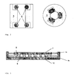
- the roller glide comprises six rollers, arranged in a bushing and is being mounted on the reactor bottom.
- the bottom end of the lift pin (1) is, at least during the lifting operation, in contact with the the elevator system via a sole plate, comprising a top plate (7) being laterally movable relative to said elevator system.
- the sole plate further comprises a ball holding plate (8) with balls (9) being arranged beyond the top plate (7), which again may be laterally movable relative to said elevator system.
- the top end of the lift pin (1) further comprises a clearance being construed to hold a rolling ball (14) being supported by a ball bearing (13) and secured by a retaining ring.
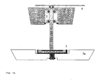
- Figure 1a shows the assembly of a pin system: A pin 1 is guided by the roller glide 2 and is actuated by the sole plate 3, which is mounted to a lift-arm 3a. At least three of these pin systems are applied for supporting and lifting a substrate 4.
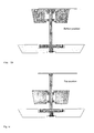
- the pins are supposed to receive the substrate 4 from a robot fork (not shown in Figure 1 ) that places the substrate on the elevating pins. Then, the pins pose the substrate 4 on the reactor bottom 2a ( Fig. 1b ). This is the substrate's final position before the coating process starts. After the coating process has ended, the pins lift the substrate in the elevated position ( Fig. 1 c) before a robot fork removes the substrate from the coating chamber.
- the inventive pin system comprises three elements: a roller glide, a ball bearing sole plate and a ball-bearing head pin.
- the first of the presented elements is the roller glide 2.
- This roller glide is designed for reducing the friction of the pin movement in a vertical axis.
- the roller glide is mounted on the reactor bottom 2a and guides the pin.
- the glide (see Fig. 2 ) consists of e. g. six rollers 6, 6 a, b, c that are made out of a material allowing low friction and low wear with the axis and bushing, chemically resistant against the process gases, and which keeps its properties at the process temperature.
- the rollers itself are held by bushing (5) made of such a material.
- a second element defines the interface between the pin and the elevator (see Fig. 3 ) : A ball bearing sole plate.
- This sole plate minimizes the lateral forces that could act on the pin.
- the lateral forces are induced by the lift-arm due to its lifting movement that does not match perfectly the pin's vertical movement axis.
- the sole plate comprises four main elements: the top plate 7 and the ball holding plate 8 that are elastically borne on the bottom plate 10. Balls 9 improve the top plate's lateral freedom of movement and hence minimize the lateral forces that act on the pin.
- the elastic bearing 7a, 8a of the top plate 7 and the ball holding plate 8 is needed for re-centering said two plates after one pin moving cycle.
- the restoring force of the elastic bearing e. g. a spring is a limiting factor for the lateral force that can be transmitted on the pin. Therefore, the spring constant should be relatively low to permit the floating movement of the top plate 7.
- the third element according to the invention is a pin ball-bearing head.
- the function of this modified pin head is to reduce the lateral forces that act on the pin. These forces may be introduced by the substrate.
- the pin head consists of a pin end 11 with a hemispherical clearance and a retaining ring 12, which holds a ball bearing 13 and a rolling ball 14.
- the rotational freedom of movement of the rolling ball 14 is enhanced by the ball bearing 13. Thereby, the lateral forces that can be induced by the substrate are minimized.
- the retaining ring (12) is slightly thicker than the pin shaft in order to prevent the pin from falling through the roller glide.
- the inventive pin design lowers the risk of self-locking considerably.
- the features of the new solution less guiding friction paired with decoupling of lateral forces, lead to a higher yield ratio and less downtime of the coating device.
- Additional positive effects are the reduction of particles in the reactor and the reduction of the risk to scratch the substrate. Thanks to the reduced friction of the pins, the abrasive forces between the pins and its guidance, as well as between the pins and the substrate are minimized. Particle contamination and the risk to scratch the substrate of the reactor are lowered.
Landscapes
- Chemical & Material Sciences (AREA)
- Engineering & Computer Science (AREA)
- Chemical Kinetics & Catalysis (AREA)
- Materials Engineering (AREA)
- Manufacturing & Machinery (AREA)
- Computer Hardware Design (AREA)
- Microelectronics & Electronic Packaging (AREA)
- Power Engineering (AREA)
- Condensed Matter Physics & Semiconductors (AREA)
- General Chemical & Material Sciences (AREA)
- Physics & Mathematics (AREA)
- General Physics & Mathematics (AREA)
- Mechanical Engineering (AREA)
- Metallurgy (AREA)
- Organic Chemistry (AREA)
- Container, Conveyance, Adherence, Positioning, Of Wafer (AREA)
- Liquid Crystal (AREA)
- Motorcycle And Bicycle Frame (AREA)
- User Interface Of Digital Computer (AREA)
- Manufacture Of Macromolecular Shaped Articles (AREA)
Claims (13)
- Zapfenanordnung zum Heben und Halten von Substraten, aufweisend:- einen Hebezapfen (1) mit einem oberen und einem unteren Ende;- wobei das obere Ende dazu eingerichtet ist ein Substrat (4) aufzunehmen und zu halten;- wobei das untere Ende dazu eingerichtet ist, von einem Hebesystem (3a) betätigt zu werden;- wobei der Hebezapfen (1) von einer Führung beweglich gehalten wird,wobei diese Führung eine Rollenführung (2) aufweist um die Reibung der Zapfenbewegung in einer vertikalen Achse zu verringern.
- Zapfenanordnung nach Anspruch 1, wobei die Kugelführung sechs Kugeln (6) aufweist die in einer Buchse (5) angeordnet sind.
- Zapfenanordnung gemäß Anspruch 1 oder 2, wobei die Rollenführung (2) auf einem Boden der Reaktionsanlage (2a) befestigt ist.
- Zapfenanordnung nach den Ansprüchen 1 bis 3, wobei die Rollenführung (2) Rollen (6) aufweist, die aus einem Werkstoff bestehen, der wenig Verschleiß und wenig Reibung aufweist.
- Zapfenanordnung nach Anspruch 2, wobei die Rollenführung (2) und die Buchse (5) aus dem gleichen Material hergestellt sind.
- Zapfenanordnung nach Anspruch 1, wobei sich das untere Ende des Hebezapfens (1) zumindest während des Hebebetriebs durch eine Bodenplatte (3) in Berührung mit dem Hebesystem (3a) befindet.
- Zapfenanordnung nach Anspruch 6, wobei die Bodenplatte (3) eine obere Platte (7) aufweist, die in Bezug auf das Hebesystem (3a) seitwärts bewegt werden kann.
- Zapfenanordnung nach Anspruch 6 oder 7, wobei die Bodenplatte (3) weiterhin eine Kugelhalteplatte (8) aufweist, die Kugeln (9) aufweist, welche unter der oberen Platte (7) angeordnet sind.
- Zapfenanordnung nach Anspruch 8, wobei die Kugelhalteplatte (8) in Bezug auf dieses Hebesystem seitwärts beweglich ist.
- Zapfenanordnung nach Anspruch 7 oder 9, wobei die seitliche Bewegung der oberen Platte (7) und der Halteplatte (8) durch elastische Lager (7a, 8a) ermöglicht wird.
- Zapfenanordnung nach Anspruch 1, wobei das obere Ende des Hebezapfens (1) weiterhin einen Zwischenraum aufweist, der dazu eingerichtet ist, eine Rollkugel (14) aufzunehmen.
- Zapfenanordnung nach Anspruch 11, wobei die Rollkugel (14) von einem Kugellager (13) gehalten wird.
- Zapfenanordnung nach Anspruch 11 oder 12, welche weiterhin einen Haltering (12) aufweist, der den Zwischenraum abdeckt und verhindert, dass der Hebezapfen durch die Rollenführung fällt.
Applications Claiming Priority (2)
| Application Number | Priority Date | Filing Date | Title |
|---|---|---|---|
| US57515804P | 2004-05-28 | 2004-05-28 | |
| PCT/CH2005/000299 WO2005117097A1 (en) | 2004-05-28 | 2005-05-26 | Lift pin with roller glide for reducing friction |
Publications (2)
| Publication Number | Publication Date |
|---|---|
| EP1754254A1 EP1754254A1 (de) | 2007-02-21 |
| EP1754254B1 true EP1754254B1 (de) | 2008-05-28 |
Family
ID=34968080
Family Applications (1)
| Application Number | Title | Priority Date | Filing Date |
|---|---|---|---|
| EP05742317A Not-in-force EP1754254B1 (de) | 2004-05-28 | 2005-05-26 | Hebezapfen mit walzenschieber zur verringerung der reibung |
Country Status (9)
| Country | Link |
|---|---|
| US (1) | US20060016398A1 (de) |
| EP (1) | EP1754254B1 (de) |
| JP (1) | JP4777345B2 (de) |
| KR (1) | KR20070032960A (de) |
| AT (1) | ATE397288T1 (de) |
| DE (1) | DE602005007217D1 (de) |
| ES (1) | ES2304174T3 (de) |
| TW (1) | TWI393799B (de) |
| WO (1) | WO2005117097A1 (de) |
Families Citing this family (23)
| Publication number | Priority date | Publication date | Assignee | Title |
|---|---|---|---|---|
| US8033245B2 (en) * | 2004-02-12 | 2011-10-11 | Applied Materials, Inc. | Substrate support bushing |
| JP2007207807A (ja) * | 2006-01-31 | 2007-08-16 | Hitachi Kokusai Electric Inc | 試料位置決め装置 |
| JP4855097B2 (ja) * | 2006-02-14 | 2012-01-18 | 株式會社塩山製作所 | 半導体チップ分離装置 |
| KR101404009B1 (ko) * | 2007-12-21 | 2014-06-13 | 주성엔지니어링(주) | 리프트 핀 어셈블리 |
| KR100945178B1 (ko) * | 2008-04-24 | 2010-03-03 | 이옥기 | 이송장치용 부싱 |
| US9011602B2 (en) * | 2009-01-29 | 2015-04-21 | Lam Research Corporation | Pin lifting system |
| WO2011009007A2 (en) * | 2009-07-15 | 2011-01-20 | Applied Materials, Inc. | Improved lift pin guides |
| JP5549441B2 (ja) * | 2010-01-14 | 2014-07-16 | 東京エレクトロン株式会社 | 保持体機構、ロードロック装置、処理装置及び搬送機構 |
| KR101053565B1 (ko) * | 2010-10-11 | 2011-08-03 | (주) 에스디시 | 승강 핀 가이드 |
| US9371584B2 (en) * | 2011-03-09 | 2016-06-21 | Applied Materials, Inc. | Processing chamber and method for centering a substrate therein |
| WO2012157638A1 (ja) * | 2011-05-19 | 2012-11-22 | シャープ株式会社 | 基板載置台および基板処理装置 |
| WO2013058970A1 (en) * | 2011-10-20 | 2013-04-25 | Applied Materials, Inc. | Substrate support bushing |
| KR101432152B1 (ko) * | 2012-11-13 | 2014-08-22 | 삼성디스플레이 주식회사 | 기판 지지 모듈 |
| CN105331947B (zh) * | 2014-05-30 | 2018-08-24 | 北京北方华创微电子装备有限公司 | 一种用于真空镀膜设备中的顶针升降机构 |
| CN105039934A (zh) * | 2015-09-15 | 2015-11-11 | 京东方科技集团股份有限公司 | 滚轮套筒 |
| KR101764418B1 (ko) | 2016-01-06 | 2017-08-02 | (주)신산이엔지 | 기판 열처리용 내열 지지유닛 |
| US10998219B2 (en) * | 2016-06-13 | 2021-05-04 | Taiwan Semiconductor Manufacturing Co., Ltd. | Wafer support device and method for removing lift pin therefrom |
| CN111971785A (zh) * | 2018-03-27 | 2020-11-20 | Vat控股公司 | 具有用于容纳和放开支撑销的联接装置的销提升装置 |
| CN111029236A (zh) * | 2018-10-09 | 2020-04-17 | 北京北方华创微电子装备有限公司 | 支撑装置及反应腔室 |
| JP7147527B2 (ja) | 2018-12-10 | 2022-10-05 | トヨタ自動車株式会社 | 支援装置、支援方法およびプログラム |
| US20220406645A1 (en) * | 2019-11-22 | 2022-12-22 | Lam Research Corporation | Coin-slot and ball-lock ceramic lift pin holders |
| CN113764328A (zh) * | 2020-06-02 | 2021-12-07 | 拓荆科技股份有限公司 | 用于加工晶圆的装置及方法 |
| DE102020120732A1 (de) * | 2020-08-06 | 2022-02-10 | Vat Holding Ag | Stifthubvorrichtung |
Family Cites Families (21)
| Publication number | Priority date | Publication date | Assignee | Title |
|---|---|---|---|---|
| US3887247A (en) * | 1974-02-25 | 1975-06-03 | Us Energy | Bearing mounting for telescoping tubes |
| JP3249765B2 (ja) * | 1997-05-07 | 2002-01-21 | 東京エレクトロン株式会社 | 基板処理装置 |
| JP3028462B2 (ja) * | 1995-05-12 | 2000-04-04 | 東京エレクトロン株式会社 | 熱処理装置 |
| JP3354367B2 (ja) * | 1995-12-19 | 2002-12-09 | 大日本スクリーン製造株式会社 | 基板洗浄装置 |
| JP3940190B2 (ja) * | 1996-09-30 | 2007-07-04 | 松下電器産業株式会社 | 真空処理装置 |
| US5672010A (en) * | 1996-11-18 | 1997-09-30 | Macnicol; Allan E. | Linear slide bearing apparatus |
| US5848670A (en) * | 1996-12-04 | 1998-12-15 | Applied Materials, Inc. | Lift pin guidance apparatus |
| JP3456890B2 (ja) * | 1998-01-16 | 2003-10-14 | 東京エレクトロン株式会社 | 基板処理装置 |
| JPH11351250A (ja) * | 1998-06-12 | 1999-12-24 | Sony Corp | ベアリング装置 |
| JP3398936B2 (ja) * | 1999-04-09 | 2003-04-21 | 日本エー・エス・エム株式会社 | 半導体処理装置 |
| JP4402763B2 (ja) * | 1999-05-13 | 2010-01-20 | Sumco Techxiv株式会社 | エピタキシャルウェーハ製造装置 |
| JP2001093960A (ja) * | 1999-09-22 | 2001-04-06 | Hitachi Techno Eng Co Ltd | 処理装置用ウエファ位置決め装置 |
| US6958098B2 (en) * | 2000-02-28 | 2005-10-25 | Applied Materials, Inc. | Semiconductor wafer support lift-pin assembly |
| US20030072639A1 (en) * | 2001-10-17 | 2003-04-17 | Applied Materials, Inc. | Substrate support |
| JP4111703B2 (ja) * | 2001-10-19 | 2008-07-02 | アプライド マテリアルズ インコーポレイテッド | ウエハリフト機構 |
| JP2003197719A (ja) * | 2001-12-21 | 2003-07-11 | Komatsu Electronic Metals Co Ltd | 半導体製造装置および基板支持構造 |
| JP2004026365A (ja) * | 2002-06-24 | 2004-01-29 | Dainippon Printing Co Ltd | 作業台 |
| DE10232478A1 (de) * | 2002-07-17 | 2004-02-12 | Infineon Technologies Ag | Waferhubvorrichtung |
| US6887317B2 (en) * | 2002-09-10 | 2005-05-03 | Applied Materials, Inc. | Reduced friction lift pin |
| JP4175988B2 (ja) * | 2002-10-25 | 2008-11-05 | 東京エレクトロン株式会社 | 基板アライメント装置及び基板処理装置及び基板搬送装置 |
| US8033245B2 (en) * | 2004-02-12 | 2011-10-11 | Applied Materials, Inc. | Substrate support bushing |
-
2005
- 2005-05-25 US US11/137,230 patent/US20060016398A1/en not_active Abandoned
- 2005-05-26 DE DE602005007217T patent/DE602005007217D1/de active Active
- 2005-05-26 EP EP05742317A patent/EP1754254B1/de not_active Not-in-force
- 2005-05-26 ES ES05742317T patent/ES2304174T3/es active Active
- 2005-05-26 WO PCT/CH2005/000299 patent/WO2005117097A1/en active IP Right Grant
- 2005-05-26 KR KR1020067027409A patent/KR20070032960A/ko not_active Application Discontinuation
- 2005-05-26 JP JP2007513650A patent/JP4777345B2/ja not_active Expired - Fee Related
- 2005-05-26 AT AT05742317T patent/ATE397288T1/de not_active IP Right Cessation
- 2005-05-27 TW TW094117365A patent/TWI393799B/zh not_active IP Right Cessation
Also Published As
| Publication number | Publication date |
|---|---|
| JP2008500709A (ja) | 2008-01-10 |
| ATE397288T1 (de) | 2008-06-15 |
| US20060016398A1 (en) | 2006-01-26 |
| ES2304174T3 (es) | 2008-09-16 |
| EP1754254A1 (de) | 2007-02-21 |
| JP4777345B2 (ja) | 2011-09-21 |
| KR20070032960A (ko) | 2007-03-23 |
| TWI393799B (zh) | 2013-04-21 |
| WO2005117097A1 (en) | 2005-12-08 |
| DE602005007217D1 (de) | 2008-07-10 |
| TW200624587A (en) | 2006-07-16 |
Similar Documents
| Publication | Publication Date | Title |
|---|---|---|
| EP1754254B1 (de) | Hebezapfen mit walzenschieber zur verringerung der reibung | |
| US11887879B2 (en) | In-situ apparatus for semiconductor process module | |
| US20190304825A1 (en) | Dual temperature heater | |
| US5951776A (en) | Self aligning lift mechanism | |
| US20050180737A1 (en) | Substrate support bushing | |
| JP5059019B2 (ja) | モールドプレス成形型、及び成形体の製造方法 | |
| US20110164955A1 (en) | Processing chamber with translating wear plate for lift pin | |
| KR20180126082A (ko) | 기판 세정 장치 및 기판 처리 장치 | |
| WO2011009007A2 (en) | Improved lift pin guides | |
| CN100409424C (zh) | 基板处理装置 | |
| KR20190057404A (ko) | 반도체 프로세싱용 웨이퍼 포지셔닝 페데스탈의 패드 상승 메커니즘 | |
| CN110739252B (zh) | 半导体加工设备 | |
| US20040219006A1 (en) | Lift pin assembly for substrate processing | |
| TWI253676B (en) | A pin set for a reactor | |
| US7075323B2 (en) | Large substrate test system | |
| KR20090056204A (ko) | 기판 승강 장치 | |
| KR101207771B1 (ko) | 마찰력을 감소시킨 리프트 핀 홀더 | |
| CN206710743U (zh) | 一种载台结构 | |
| KR100375984B1 (ko) | 플레이트 어셈블리 및 이를 갖는 가공 장치 | |
| CN112447580A (zh) | 具有滑动引导件的销升降装置 | |
| JP2008239467A (ja) | モールドプレス成形型、及び成形体の製造方法 | |
| KR101381207B1 (ko) | 가동부재를 가지는 기판지지핀 홀더 및 이를 포함하는기판처리장치 | |
| US20230178416A1 (en) | Floating pin for substrate transfer | |
| JP4914139B2 (ja) | 半導体処理装置 | |
| JP2006083026A (ja) | モールドプレス成形型および成形体の製造方法 |
Legal Events
| Date | Code | Title | Description |
|---|---|---|---|
| PUAI | Public reference made under article 153(3) epc to a published international application that has entered the european phase |
Free format text: ORIGINAL CODE: 0009012 |
|
| 17P | Request for examination filed |
Effective date: 20061228 |
|
| AK | Designated contracting states |
Kind code of ref document: A1 Designated state(s): AT BE BG CH CY CZ DE DK EE ES FI FR GB GR HU IE IS IT LI LT LU MC NL PL PT RO SE SI SK TR |
|
| RIN1 | Information on inventor provided before grant (corrected) |
Inventor name: HERNANDEZ, SYLVAIN Inventor name: SCHMITT, JACQUES Inventor name: JAEGER, HANS Inventor name: EL BOUCHIKHY, REDOUANE Inventor name: LANDRY, KARINE Inventor name: DUBOST, LAURENT Inventor name: ZAPODEANU, EUGENE Inventor name: VINEL, BERTRAND |
|
| DAX | Request for extension of the european patent (deleted) | ||
| GRAP | Despatch of communication of intention to grant a patent |
Free format text: ORIGINAL CODE: EPIDOSNIGR1 |
|
| GRAS | Grant fee paid |
Free format text: ORIGINAL CODE: EPIDOSNIGR3 |
|
| GRAA | (expected) grant |
Free format text: ORIGINAL CODE: 0009210 |
|
| AK | Designated contracting states |
Kind code of ref document: B1 Designated state(s): AT BE BG CH CY CZ DE DK EE ES FI FR GB GR HU IE IS IT LI LT LU MC NL PL PT RO SE SI SK TR |
|
| REG | Reference to a national code |
Ref country code: GB Ref legal event code: FG4D |
|
| REG | Reference to a national code |
Ref country code: CH Ref legal event code: EP |
|
| REF | Corresponds to: |
Ref document number: 602005007217 Country of ref document: DE Date of ref document: 20080710 Kind code of ref document: P |
|
| REG | Reference to a national code |
Ref country code: IE Ref legal event code: FG4D |
|
| REG | Reference to a national code |
Ref country code: ES Ref legal event code: FG2A Ref document number: 2304174 Country of ref document: ES Kind code of ref document: T3 |
|
| PG25 | Lapsed in a contracting state [announced via postgrant information from national office to epo] |
Ref country code: SI Free format text: LAPSE BECAUSE OF FAILURE TO SUBMIT A TRANSLATION OF THE DESCRIPTION OR TO PAY THE FEE WITHIN THE PRESCRIBED TIME-LIMIT Effective date: 20080528 |
|
| PG25 | Lapsed in a contracting state [announced via postgrant information from national office to epo] |
Ref country code: FI Free format text: LAPSE BECAUSE OF FAILURE TO SUBMIT A TRANSLATION OF THE DESCRIPTION OR TO PAY THE FEE WITHIN THE PRESCRIBED TIME-LIMIT Effective date: 20080528 |
|
| PG25 | Lapsed in a contracting state [announced via postgrant information from national office to epo] |
Ref country code: AT Free format text: LAPSE BECAUSE OF FAILURE TO SUBMIT A TRANSLATION OF THE DESCRIPTION OR TO PAY THE FEE WITHIN THE PRESCRIBED TIME-LIMIT Effective date: 20080528 Ref country code: NL Free format text: LAPSE BECAUSE OF FAILURE TO SUBMIT A TRANSLATION OF THE DESCRIPTION OR TO PAY THE FEE WITHIN THE PRESCRIBED TIME-LIMIT Effective date: 20080528 |
|
| NLV1 | Nl: lapsed or annulled due to failure to fulfill the requirements of art. 29p and 29m of the patents act | ||
| ET | Fr: translation filed | ||
| PG25 | Lapsed in a contracting state [announced via postgrant information from national office to epo] |
Ref country code: IS Free format text: LAPSE BECAUSE OF FAILURE TO SUBMIT A TRANSLATION OF THE DESCRIPTION OR TO PAY THE FEE WITHIN THE PRESCRIBED TIME-LIMIT Effective date: 20080928 |
|
| PG25 | Lapsed in a contracting state [announced via postgrant information from national office to epo] |
Ref country code: DK Free format text: LAPSE BECAUSE OF FAILURE TO SUBMIT A TRANSLATION OF THE DESCRIPTION OR TO PAY THE FEE WITHIN THE PRESCRIBED TIME-LIMIT Effective date: 20080528 Ref country code: LT Free format text: LAPSE BECAUSE OF FAILURE TO SUBMIT A TRANSLATION OF THE DESCRIPTION OR TO PAY THE FEE WITHIN THE PRESCRIBED TIME-LIMIT Effective date: 20080528 Ref country code: CZ Free format text: LAPSE BECAUSE OF FAILURE TO SUBMIT A TRANSLATION OF THE DESCRIPTION OR TO PAY THE FEE WITHIN THE PRESCRIBED TIME-LIMIT Effective date: 20080528 Ref country code: SE Free format text: LAPSE BECAUSE OF FAILURE TO SUBMIT A TRANSLATION OF THE DESCRIPTION OR TO PAY THE FEE WITHIN THE PRESCRIBED TIME-LIMIT Effective date: 20080828 |
|
| PG25 | Lapsed in a contracting state [announced via postgrant information from national office to epo] |
Ref country code: RO Free format text: LAPSE BECAUSE OF FAILURE TO SUBMIT A TRANSLATION OF THE DESCRIPTION OR TO PAY THE FEE WITHIN THE PRESCRIBED TIME-LIMIT Effective date: 20080528 Ref country code: SK Free format text: LAPSE BECAUSE OF FAILURE TO SUBMIT A TRANSLATION OF THE DESCRIPTION OR TO PAY THE FEE WITHIN THE PRESCRIBED TIME-LIMIT Effective date: 20080528 Ref country code: BE Free format text: LAPSE BECAUSE OF FAILURE TO SUBMIT A TRANSLATION OF THE DESCRIPTION OR TO PAY THE FEE WITHIN THE PRESCRIBED TIME-LIMIT Effective date: 20080528 Ref country code: PT Free format text: LAPSE BECAUSE OF FAILURE TO SUBMIT A TRANSLATION OF THE DESCRIPTION OR TO PAY THE FEE WITHIN THE PRESCRIBED TIME-LIMIT Effective date: 20081028 |
|
| PLBE | No opposition filed within time limit |
Free format text: ORIGINAL CODE: 0009261 |
|
| STAA | Information on the status of an ep patent application or granted ep patent |
Free format text: STATUS: NO OPPOSITION FILED WITHIN TIME LIMIT |
|
| PG25 | Lapsed in a contracting state [announced via postgrant information from national office to epo] |
Ref country code: BG Free format text: LAPSE BECAUSE OF FAILURE TO SUBMIT A TRANSLATION OF THE DESCRIPTION OR TO PAY THE FEE WITHIN THE PRESCRIBED TIME-LIMIT Effective date: 20080828 Ref country code: EE Free format text: LAPSE BECAUSE OF FAILURE TO SUBMIT A TRANSLATION OF THE DESCRIPTION OR TO PAY THE FEE WITHIN THE PRESCRIBED TIME-LIMIT Effective date: 20080528 |
|
| 26N | No opposition filed |
Effective date: 20090303 |
|
| PGFP | Annual fee paid to national office [announced via postgrant information from national office to epo] |
Ref country code: ES Payment date: 20090605 Year of fee payment: 5 |
|
| PGFP | Annual fee paid to national office [announced via postgrant information from national office to epo] |
Ref country code: IT Payment date: 20090520 Year of fee payment: 5 |
|
| PGFP | Annual fee paid to national office [announced via postgrant information from national office to epo] |
Ref country code: GB Payment date: 20090520 Year of fee payment: 5 |
|
| PG25 | Lapsed in a contracting state [announced via postgrant information from national office to epo] |
Ref country code: MC Free format text: LAPSE BECAUSE OF NON-PAYMENT OF DUE FEES Effective date: 20090531 |
|
| REG | Reference to a national code |
Ref country code: CH Ref legal event code: PL |
|
| PG25 | Lapsed in a contracting state [announced via postgrant information from national office to epo] |
Ref country code: CH Free format text: LAPSE BECAUSE OF NON-PAYMENT OF DUE FEES Effective date: 20090531 Ref country code: LI Free format text: LAPSE BECAUSE OF NON-PAYMENT OF DUE FEES Effective date: 20090531 |
|
| REG | Reference to a national code |
Ref country code: IE Ref legal event code: MM4A |
|
| PG25 | Lapsed in a contracting state [announced via postgrant information from national office to epo] |
Ref country code: IE Free format text: LAPSE BECAUSE OF NON-PAYMENT OF DUE FEES Effective date: 20090526 |
|
| PG25 | Lapsed in a contracting state [announced via postgrant information from national office to epo] |
Ref country code: PL Free format text: LAPSE BECAUSE OF FAILURE TO SUBMIT A TRANSLATION OF THE DESCRIPTION OR TO PAY THE FEE WITHIN THE PRESCRIBED TIME-LIMIT Effective date: 20080528 |
|
| PG25 | Lapsed in a contracting state [announced via postgrant information from national office to epo] |
Ref country code: GR Free format text: LAPSE BECAUSE OF FAILURE TO SUBMIT A TRANSLATION OF THE DESCRIPTION OR TO PAY THE FEE WITHIN THE PRESCRIBED TIME-LIMIT Effective date: 20080829 |
|
| GBPC | Gb: european patent ceased through non-payment of renewal fee |
Effective date: 20100526 |
|
| PG25 | Lapsed in a contracting state [announced via postgrant information from national office to epo] |
Ref country code: IT Free format text: LAPSE BECAUSE OF NON-PAYMENT OF DUE FEES Effective date: 20100526 |
|
| PG25 | Lapsed in a contracting state [announced via postgrant information from national office to epo] |
Ref country code: LU Free format text: LAPSE BECAUSE OF NON-PAYMENT OF DUE FEES Effective date: 20090526 |
|
| PG25 | Lapsed in a contracting state [announced via postgrant information from national office to epo] |
Ref country code: HU Free format text: LAPSE BECAUSE OF FAILURE TO SUBMIT A TRANSLATION OF THE DESCRIPTION OR TO PAY THE FEE WITHIN THE PRESCRIBED TIME-LIMIT Effective date: 20081129 |
|
| REG | Reference to a national code |
Ref country code: ES Ref legal event code: FD2A Effective date: 20110711 |
|
| PG25 | Lapsed in a contracting state [announced via postgrant information from national office to epo] |
Ref country code: ES Free format text: LAPSE BECAUSE OF NON-PAYMENT OF DUE FEES Effective date: 20110629 Ref country code: GB Free format text: LAPSE BECAUSE OF NON-PAYMENT OF DUE FEES Effective date: 20100526 |
|
| PG25 | Lapsed in a contracting state [announced via postgrant information from national office to epo] |
Ref country code: TR Free format text: LAPSE BECAUSE OF FAILURE TO SUBMIT A TRANSLATION OF THE DESCRIPTION OR TO PAY THE FEE WITHIN THE PRESCRIBED TIME-LIMIT Effective date: 20080528 |
|
| PG25 | Lapsed in a contracting state [announced via postgrant information from national office to epo] |
Ref country code: CY Free format text: LAPSE BECAUSE OF FAILURE TO SUBMIT A TRANSLATION OF THE DESCRIPTION OR TO PAY THE FEE WITHIN THE PRESCRIBED TIME-LIMIT Effective date: 20080528 Ref country code: ES Free format text: LAPSE BECAUSE OF NON-PAYMENT OF DUE FEES Effective date: 20100527 |
|
| REG | Reference to a national code |
Ref country code: DE Ref legal event code: R082 Ref document number: 602005007217 Country of ref document: DE Representative=s name: MICHALSKI HUETTERMANN & PARTNER PATENTANWAELTE, DE |
|
| REG | Reference to a national code |
Ref country code: DE Ref legal event code: R082 Ref document number: 602005007217 Country of ref document: DE Representative=s name: MICHALSKI HUETTERMANN & PARTNER PATENTANWAELTE, DE Effective date: 20120123 Ref country code: DE Ref legal event code: R081 Ref document number: 602005007217 Country of ref document: DE Owner name: TEL SOLAR AG, CH Free format text: FORMER OWNER: OC OERLIKON BALZERS AG, BALZERS, LI Effective date: 20120123 |
|
| REG | Reference to a national code |
Ref country code: DE Ref legal event code: R082 Ref document number: 602005007217 Country of ref document: DE Representative=s name: MICHALSKI HUETTERMANN & PARTNER PATENTANWAELTE, DE |
|
| PGFP | Annual fee paid to national office [announced via postgrant information from national office to epo] |
Ref country code: FR Payment date: 20130531 Year of fee payment: 9 |
|
| REG | Reference to a national code |
Ref country code: DE Ref legal event code: R081 Ref document number: 602005007217 Country of ref document: DE Owner name: TEL SOLAR AG, CH Free format text: FORMER OWNER: OERLIKON SOLAR AG, TRUEBBACH, TRUEBBACH, CH Effective date: 20130731 Ref country code: DE Ref legal event code: R082 Ref document number: 602005007217 Country of ref document: DE Representative=s name: MICHALSKI HUETTERMANN & PARTNER PATENTANWAELTE, DE Effective date: 20130731 |
|
| PGFP | Annual fee paid to national office [announced via postgrant information from national office to epo] |
Ref country code: DE Payment date: 20140521 Year of fee payment: 10 |
|
| REG | Reference to a national code |
Ref country code: FR Ref legal event code: ST Effective date: 20150130 |
|
| PG25 | Lapsed in a contracting state [announced via postgrant information from national office to epo] |
Ref country code: FR Free format text: LAPSE BECAUSE OF NON-PAYMENT OF DUE FEES Effective date: 20140602 |
|
| REG | Reference to a national code |
Ref country code: DE Ref legal event code: R119 Ref document number: 602005007217 Country of ref document: DE |
|
| PG25 | Lapsed in a contracting state [announced via postgrant information from national office to epo] |
Ref country code: DE Free format text: LAPSE BECAUSE OF NON-PAYMENT OF DUE FEES Effective date: 20151201 |