EP1741132B1 - Method of making dual-metal cmos transistors with tunable gate electrode work function - Google Patents
Method of making dual-metal cmos transistors with tunable gate electrode work function Download PDFInfo
- Publication number
- EP1741132B1 EP1741132B1 EP05736767A EP05736767A EP1741132B1 EP 1741132 B1 EP1741132 B1 EP 1741132B1 EP 05736767 A EP05736767 A EP 05736767A EP 05736767 A EP05736767 A EP 05736767A EP 1741132 B1 EP1741132 B1 EP 1741132B1
- Authority
- EP
- European Patent Office
- Prior art keywords
- silicon
- regions
- metal
- silicide
- layer
- Prior art date
- Legal status (The legal status is an assumption and is not a legal conclusion. Google has not performed a legal analysis and makes no representation as to the accuracy of the status listed.)
- Expired - Lifetime
Links
Images


Classifications
-
- H—ELECTRICITY
- H10—SEMICONDUCTOR DEVICES; ELECTRIC SOLID-STATE DEVICES NOT OTHERWISE PROVIDED FOR
- H10D—INORGANIC ELECTRIC SEMICONDUCTOR DEVICES
- H10D84/00—Integrated devices formed in or on semiconductor substrates that comprise only semiconducting layers, e.g. on Si wafers or on GaAs-on-Si wafers
- H10D84/01—Manufacture or treatment
- H10D84/0123—Integrating together multiple components covered by H10D12/00 or H10D30/00, e.g. integrating multiple IGBTs
- H10D84/0126—Integrating together multiple components covered by H10D12/00 or H10D30/00, e.g. integrating multiple IGBTs the components including insulated gates, e.g. IGFETs
- H10D84/0165—Integrating together multiple components covered by H10D12/00 or H10D30/00, e.g. integrating multiple IGBTs the components including insulated gates, e.g. IGFETs the components including complementary IGFETs, e.g. CMOS devices
-
- H—ELECTRICITY
- H01—ELECTRIC ELEMENTS
- H01L—SEMICONDUCTOR DEVICES NOT COVERED BY CLASS H10
- H01L21/00—Processes or apparatus adapted for the manufacture or treatment of semiconductor or solid state devices or of parts thereof
- H01L21/02—Manufacture or treatment of semiconductor devices or of parts thereof
- H01L21/04—Manufacture or treatment of semiconductor devices or of parts thereof the devices having potential barriers, e.g. a PN junction, depletion layer or carrier concentration layer
- H01L21/18—Manufacture or treatment of semiconductor devices or of parts thereof the devices having potential barriers, e.g. a PN junction, depletion layer or carrier concentration layer the devices having semiconductor bodies comprising elements of Group IV of the Periodic Table or AIIIBV compounds with or without impurities, e.g. doping materials
-
- H—ELECTRICITY
- H10—SEMICONDUCTOR DEVICES; ELECTRIC SOLID-STATE DEVICES NOT OTHERWISE PROVIDED FOR
- H10D—INORGANIC ELECTRIC SEMICONDUCTOR DEVICES
- H10D84/00—Integrated devices formed in or on semiconductor substrates that comprise only semiconducting layers, e.g. on Si wafers or on GaAs-on-Si wafers
- H10D84/01—Manufacture or treatment
- H10D84/0123—Integrating together multiple components covered by H10D12/00 or H10D30/00, e.g. integrating multiple IGBTs
- H10D84/0126—Integrating together multiple components covered by H10D12/00 or H10D30/00, e.g. integrating multiple IGBTs the components including insulated gates, e.g. IGFETs
- H10D84/0165—Integrating together multiple components covered by H10D12/00 or H10D30/00, e.g. integrating multiple IGBTs the components including insulated gates, e.g. IGFETs the components including complementary IGFETs, e.g. CMOS devices
- H10D84/0172—Manufacturing their gate conductors
- H10D84/0174—Manufacturing their gate conductors the gate conductors being silicided
-
- H—ELECTRICITY
- H10—SEMICONDUCTOR DEVICES; ELECTRIC SOLID-STATE DEVICES NOT OTHERWISE PROVIDED FOR
- H10D—INORGANIC ELECTRIC SEMICONDUCTOR DEVICES
- H10D84/00—Integrated devices formed in or on semiconductor substrates that comprise only semiconducting layers, e.g. on Si wafers or on GaAs-on-Si wafers
- H10D84/01—Manufacture or treatment
- H10D84/0123—Integrating together multiple components covered by H10D12/00 or H10D30/00, e.g. integrating multiple IGBTs
- H10D84/0126—Integrating together multiple components covered by H10D12/00 or H10D30/00, e.g. integrating multiple IGBTs the components including insulated gates, e.g. IGFETs
- H10D84/0165—Integrating together multiple components covered by H10D12/00 or H10D30/00, e.g. integrating multiple IGBTs the components including insulated gates, e.g. IGFETs the components including complementary IGFETs, e.g. CMOS devices
- H10D84/0172—Manufacturing their gate conductors
- H10D84/0177—Manufacturing their gate conductors the gate conductors having different materials or different implants
-
- H—ELECTRICITY
- H10—SEMICONDUCTOR DEVICES; ELECTRIC SOLID-STATE DEVICES NOT OTHERWISE PROVIDED FOR
- H10D—INORGANIC ELECTRIC SEMICONDUCTOR DEVICES
- H10D84/00—Integrated devices formed in or on semiconductor substrates that comprise only semiconducting layers, e.g. on Si wafers or on GaAs-on-Si wafers
- H10D84/01—Manufacture or treatment
- H10D84/02—Manufacture or treatment characterised by using material-based technologies
- H10D84/03—Manufacture or treatment characterised by using material-based technologies using Group IV technology, e.g. silicon technology or silicon-carbide [SiC] technology
- H10D84/038—Manufacture or treatment characterised by using material-based technologies using Group IV technology, e.g. silicon technology or silicon-carbide [SiC] technology using silicon technology, e.g. SiGe
-
- H—ELECTRICITY
- H01—ELECTRIC ELEMENTS
- H01L—SEMICONDUCTOR DEVICES NOT COVERED BY CLASS H10
- H01L21/00—Processes or apparatus adapted for the manufacture or treatment of semiconductor or solid state devices or of parts thereof
- H01L21/02—Manufacture or treatment of semiconductor devices or of parts thereof
- H01L21/04—Manufacture or treatment of semiconductor devices or of parts thereof the devices having potential barriers, e.g. a PN junction, depletion layer or carrier concentration layer
- H01L21/18—Manufacture or treatment of semiconductor devices or of parts thereof the devices having potential barriers, e.g. a PN junction, depletion layer or carrier concentration layer the devices having semiconductor bodies comprising elements of Group IV of the Periodic Table or AIIIBV compounds with or without impurities, e.g. doping materials
- H01L21/28—Manufacture of electrodes on semiconductor bodies using processes or apparatus not provided for in groups H01L21/20 - H01L21/268
- H01L21/28008—Making conductor-insulator-semiconductor electrodes
- H01L21/28017—Making conductor-insulator-semiconductor electrodes the insulator being formed after the semiconductor body, the semiconductor being silicon
- H01L21/28026—Making conductor-insulator-semiconductor electrodes the insulator being formed after the semiconductor body, the semiconductor being silicon characterised by the conductor
- H01L21/28097—Making conductor-insulator-semiconductor electrodes the insulator being formed after the semiconductor body, the semiconductor being silicon characterised by the conductor the final conductor layer next to the insulator being a metallic silicide
Definitions
- the present invention relates to the field of semiconductor fabrication, and more particularly, to a fabrication process incorporating different gate metals for NMOS and PMOS devices.
- NMOS N-type metal oxide semiconductors
- PMOS P-type metal oxide semiconductor
- the NMOS and PMOS threshold voltages are conventionally adjusted by a combination of channel implants and selective doping of a polysilicon gate. It is generally effective in adjusting the threshold voltages for PMOS devices but less effective for NMOS devices.
- dual metal gate CMOS complementary MOS
- CMOS arrangement comprising a substrate and a plurality of NMOS devices and a plurality of PMOS devices.
- the plurality of NMOS devices have gate electrodes, with each NMOS gate electrode including a first silicide region on the substrate and a first metal region on the first silicide region.
- the first silicide region of the NMOS gate electrode consists of a first silicide having a work function within +/- 0.2V of the conduction band of silicon.
- the plurality of PMOS devices have gate electrodes, with each PMOS gate electrode having a second silicide region on the substrate and a second metal region on the second silicide region.
- the second silicide region of the PMOS gate electrode consists of a second silicide having a work function within +/- 0.2V of the valence band of silicon.
- the other stated needs are also met by other aspects of the present invention which provide a method of forming a dual-metal CMOS arrangement, comprising the steps of forming silicon regions on gate dielectrics to form gate electrodes in NMOS device regions and in PMOS device regions.
- the silicon regions are converted to a first silicide region in the NMOS device regions and to a second silicide region in the PMOS device regions.
- the first silicide region consists of a first silicide having a work function within +/- 0.2V of the conduction band of silicon and the second silicide region consists of a second silicide having a work function that is within +/- 0.2V of the valence band of silicon.
- the invention addresses a method of forming a dual metal CMOS arrangement as recited in claim 1.
- the present invention addresses and solves problems related to the formation of dual-metal CMOS transistors, and in particular, to those problems associated with fully silicided gate electrodes, including those related to non-uniformity of silicidation and gate oxide reliability.
- the dual-metal CMOS arrangement is provided with a plurality of NMOS devices and PMOS devices that have gate electrodes.
- Each NMOS gate electrode includes a first silicide region on the substrate and a first metal region on the first silicide region.
- the first silicide region of the NMOS gate electrode consists of a first silicide having a work function within +/- 0.2 V of the conduction band of silicon.
- Each PMOS gate electrode includes a second silicide region on the substrate and a second metal region on the second silicide region.
- the second silicide regions of the PMOS gate electrodes consist of a second silicide having a work function within +/- 0.2 V of the valence band of silicon.
- each gate electrode is only partially silicided, and the silicide regions are respectively provided with silicide that is tunable to be compatible with the NMOS and PMOS type devices.
- the tuning of the work function is achieved employing two different kinds of metals, such as the silicide regions are formed with two different metal silicides having different work functions.
- the silicide thickness is precisely adjusted to achieve certain silicide phases, thereby affecting the work function of these silicides for the respective NMOS and PMOS type devices.
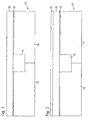
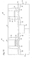
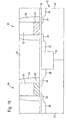
- Fig. 1 depicts a cross-sectional view of a portion of a semiconductor wafer during one stage of a semiconductor manufacturing process according to embodiments of the present invention.
- a partially completed semiconductor device is illustrated in Fig. 1 .
- the device includes a substrate 10 formed of silicon, for example.
- Substrate 10 includes a P-doped region 12 and an N-doped region 14.
- the substrate 10 is doped with the N- or P-type dopants with a dose of about 1x10 16 to about 1x10 21 ion/cm 2 , for example.
- a shallow trench isolation (STI) structure 16 provides separation between the P-doped region 12 and the N-doped region 14 at the device level.
- Conventional STI formation methodology may be employed to create the shallow trench isolation region 16.
- a gate dielectric layer 18 is formed on the substrate 10.
- the gate dielectric layer 18 may consist of a gate oxide, for example.
- the gate dielectric layer 18 is ultra-thin, and may be between about 5 to about 30 ⁇ , for example.
- Such a thin gate dielectric layer is readily susceptible to damage during a metal dry etch process, so that a silicide process has certain advantages. However, a fully silicided gate formation process can overstress the gate oxide.
- a first silicon layer 20 is formed on the gate dielectric layer 18.
- the first silicon layer 20 may be deposited in a conventional manner.
- the first silicon layer is relatively thin, between 10 to about 500 ⁇ , for example.
- the thickness of the first silicon layer is between 50 to about 200 ⁇ .
- the thickness of the first silicon layer is less than about 50 ⁇ .
- a relatively thin gate silicide thickness solves problems related to those created by fully silicided gate electrodes, including non-uniformity of silicidation and gate oxide reliability.
- Fig. 2 depicts the structure of Fig. 1 following the formation of an etch stop layer 22 on the first silicon layer 20.
- the etch stop layer 22 may be an oxide layer, for example. It is desirable to form the etch stop layer 22 to be very thin, such as about 10 ⁇ , for example. Any suitable method for forming such a thin layer of oxide or other etch stop material may be employed. For example, an oxidation process at 600 to 1000°C may be used to form the etch stop layer 22.
- a second layer of silicon 24 is formed by conventional methodologies on the etch stop layer 22.
- the second silicon layer 24 may be between about 700 to about 2000 ⁇ , for example, and in certain embodiments, is about 1000 ⁇ thick.
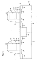
- Fig. 4 depicts the structure of Fig. 3 after a hard mask layer has been deposited on the second silicon layer 24, followed by etching steps to form silicon stacks 26.
- Each of the silicon stacks 26 has a hard mask 30 formed on the upper portion 28 of the silicon stack 26.
- the etching creates silicon regions 32 in each of the silicon stacks 26.
- the hard mask 30 may be any suitable material, such as silicon nitride, silicon oxide, etc.
- a conventional anisotropic etching technique, such as reactive ion etching, is employed to etch down to the gate dielectric layer 18.
- a source/drain extension implantation process is performed to create source/drain extensions 34.
- Conventional masking and doping techniques are performed to appropriately dope the NMOS devices and PMOS devices separately with a suitable dose of dopants.
- sidewall spacers 36 are created on the sidewalls of the silicon stack 26 by conventional techniques, such as deposition of a spacer material and etching.
- appropriate masking and implantation techniques are employed to create source/drain regions 38 in the NMOS devices and the PMOS devices, respectively.
- a dielectric layer 40 has been deposited and planarized.
- the dielectric layer 40 may be of any conventional suitable dielectric material, such as a low k dielectric, an oxide, etc.
- the dielectric layer 40 may be deposited oy any suitable methodology, such as chemical vapor deposition (CVD), etc.
- the planarization in certain ⁇ embodiments, is chemical-mechanical polishing, for example.
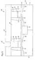
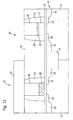
- a lithography and masking step is then performed, as depicted in Fig. 7 , in which photoresist 42 masks the PMOS devices 46 and exposes the NMOS devices 44.
- a polysilicon etch process is performed that is very selective to oxide.
- An anisotropic etch such as a reactive ion etch, can be employed. Suitable etchants include chlorine and HBrO 2 , or SF 6 , for example.
- the upper portion 28 of the silicon stack 26 is removed by this etch process. The etch stops on the etch stop layer 22 reliably. This preserves the silicon region 32.
- first metal 48 is deposited to a thickness that assures complete filling of space left by the etching of the upper portion 28 of the silicide stack 26.
- the etch stop layer 22 Prior to the depositing of the first metal 48, however, the etch stop layer 22 is removed.
- the etch stop layer 22 is an oxide, for example, a buffered oxide etch is performed to remove the etch stop layer 22. This etch is a short time wet etch, for example, to remove the very thin etch stop layer 22 without damaging the surrounding sidewall spacer 36.
- the first metal 48 is deposited to a thickness of at least 1000 ⁇ to assure complete filling of the space previously occupied by the upper portion 28 of the silicon stack 26.
- the first metal 48 is a metal or metal alloy that when reacted with silicon, forms a silicide with a work function close to the conduction band of silicon. This is defined as being within +/- 0.2V of the conduction band of silicon.
- one suitable metal is tantalum.
- the invention is not limited to tantalum, but may include other metals whose silicides are close to the conduction band of silicon.
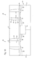
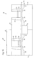
- Fig. 10 depicts the structure of Fig. 9 following the removal of the excess first metal 48, performed by a metal CMP process.
- the first metal 48 is removed until the dielectric layer 40 is reached.
- an annealing process such as rapid thermal annealing, is employed to form the first silicide region 50 in each of the NMOS devices 44.
- a suitable temperature range is employed, depending upon the type of metal or metal alloy used as the first metal 48. Such processing conditions are known to those of ordinary skill in the art.
- FIG. 12 depicts a lithography step in which the NMOS devices 44 are masked and the PMOS devices 46 are exposed.
- An etching process removes the upper portion 28 of the silicon stack 26 in each of the PMOS devices 46, as depicted in Fig. 13 .
- a second metal 52 is deposited on the dielectric layer 40 and within the space previously occupied by the upper portion 28 of the silicon stack 26.
- the second metal 52 consists of a metal or metal alloy that forms a silicide with a work function that is close to the valence band of silicon.
- the work function of the silicide is within +/- 0.2V of the valence band of silicon.
- Exemplary materials may include ruthenium, rhenium, or cobalt, for example.
- Other types of materials may be employed as a second metal 52 without departing from the scope of the present invention. However, such materials should form silicides with a work function that is close to the valence band of silicon in order to achieve the desired dual work functions of the CMOS arrangement.
- an appropriate annealing process is performed to form the second silicide regions 54 in the PMOS devices 46.
- a suitable temperature range for the annealing process is selected depending upon the metal forming the second metal 52.
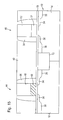
- the NMOS devices have a first silicide region 50 consisting of a first silicide having a work function within +/- 0.2V of the conduction band of silicon.
- the CMOS arrangement also has PMOS devices with second silicide regions that consist of a second silicide having a work function within +/- 0.2V of the valence band of silicon.
- the work functions of gate electrodes of the NMOS and PMOS devices 44, 46 are thus tunable by employing different kinds of metals or metal alloys to form the metal silicides.
- Figs. 17 and 18 depict certain steps in alternate embodiments of the present invention.
- the etch stop layer 22 is not employed. Instead, the silicon stack 26 is recessed by a controlled wet or dry etching to substantially reduce the polysilicon thickness of the silicon stack 26 prior to silicidation.
- the PMOS device 46 is masked and the silicon stack 26 of the NMOS device is etched. A similar process occurs to etch the silicon stack 26 in the PMOS devices 46.
- the thicknesses of the remaining silicon of the silicon stacks 26 are carefully controlled to be a desired thickness. The thickness of a thin polysilicon affects the phases of the silicide regions that are formed, which exhibit different conductivities.
- the same metal may be employed, or different metals may be employed, to form the first and second silicide regions 50, 54, respectively. This is because the thickness of the silicon regions will control the phases of the silicides that are ultimately formed.
- certain type devices may be provided with a gate electrode having a higher resistivity phase silicide, such as CoSi, and other type devices provided with a gate electrode having a lower resistivity phase silicide, such as CoSi 2 .
- annealing parameters such as time and temperature
- the annealing parameters such as time and temperature
Landscapes
- Engineering & Computer Science (AREA)
- Physics & Mathematics (AREA)
- Condensed Matter Physics & Semiconductors (AREA)
- General Physics & Mathematics (AREA)
- Manufacturing & Machinery (AREA)
- Computer Hardware Design (AREA)
- Microelectronics & Electronic Packaging (AREA)
- Power Engineering (AREA)
- Metal-Oxide And Bipolar Metal-Oxide Semiconductor Integrated Circuits (AREA)
- Electrodes Of Semiconductors (AREA)
- Insulated Gate Type Field-Effect Transistor (AREA)
Applications Claiming Priority (2)
| Application Number | Priority Date | Filing Date | Title |
|---|---|---|---|
| US10/833,073 US7078278B2 (en) | 2004-04-28 | 2004-04-28 | Dual-metal CMOS transistors with tunable gate electrode work function and method of making the same |
| PCT/US2005/013240 WO2005109493A1 (en) | 2004-04-28 | 2005-04-19 | Dual-metal cmos transistors with tunable gate electrode work function and method of making the same |
Publications (2)
| Publication Number | Publication Date |
|---|---|
| EP1741132A1 EP1741132A1 (en) | 2007-01-10 |
| EP1741132B1 true EP1741132B1 (en) | 2009-09-23 |
Family
ID=34966174
Family Applications (1)
| Application Number | Title | Priority Date | Filing Date |
|---|---|---|---|
| EP05736767A Expired - Lifetime EP1741132B1 (en) | 2004-04-28 | 2005-04-19 | Method of making dual-metal cmos transistors with tunable gate electrode work function |
Country Status (8)
| Country | Link |
|---|---|
| US (1) | US7078278B2 (enExample) |
| EP (1) | EP1741132B1 (enExample) |
| JP (1) | JP4728323B2 (enExample) |
| KR (1) | KR101125269B1 (enExample) |
| CN (1) | CN100472756C (enExample) |
| DE (1) | DE602005016790D1 (enExample) |
| TW (1) | TWI378492B (enExample) |
| WO (1) | WO2005109493A1 (enExample) |
Families Citing this family (23)
| Publication number | Priority date | Publication date | Assignee | Title |
|---|---|---|---|---|
| US7645687B2 (en) * | 2005-01-20 | 2010-01-12 | Chartered Semiconductor Manufacturing, Ltd. | Method to fabricate variable work function gates for FUSI devices |
| JP2006253316A (ja) | 2005-03-09 | 2006-09-21 | Sony Corp | 固体撮像装置 |
| JP5015446B2 (ja) * | 2005-05-16 | 2012-08-29 | アイメック | 二重の完全ケイ化ゲートを形成する方法と前記方法によって得られたデバイス |
| JP2007142127A (ja) * | 2005-11-18 | 2007-06-07 | Sony Corp | 半導体装置およびその製造方法 |
| JP2007157744A (ja) * | 2005-11-30 | 2007-06-21 | Toshiba Corp | 半導体装置および半導体装置の製造方法 |
| US7768072B2 (en) * | 2007-03-27 | 2010-08-03 | Taiwan Semiconductor Manufacturing Company, Ltd. | Silicided metal gate for multi-threshold voltage configuration |
| US7678694B2 (en) * | 2007-04-18 | 2010-03-16 | Taiwan Semicondutor Manufacturing Company, Ltd. | Method for fabricating semiconductor device with silicided gate |
| US8183137B2 (en) * | 2007-05-23 | 2012-05-22 | Texas Instruments Incorporated | Use of dopants to provide low defect gate full silicidation |
| US7642153B2 (en) * | 2007-10-23 | 2010-01-05 | Texas Instruments Incorporated | Methods for forming gate electrodes for integrated circuits |
| US8124515B2 (en) * | 2009-05-20 | 2012-02-28 | Globalfoundries Inc. | Gate etch optimization through silicon dopant profile change |
| US8895426B2 (en) * | 2009-06-12 | 2014-11-25 | Taiwan Semiconductor Manufacturing Company, Ltd. | Metal gate transistor, integrated circuits, systems, and fabrication methods thereof |
| WO2012086102A1 (ja) * | 2010-12-24 | 2012-06-28 | パナソニック株式会社 | 半導体装置及びその製造方法 |
| US8440520B2 (en) * | 2011-08-23 | 2013-05-14 | Tokyo Electron Limited | Diffused cap layers for modifying high-k gate dielectrics and interface layers |
| US8722472B2 (en) * | 2011-12-16 | 2014-05-13 | International Business Machines Corporation | Hybrid CMOS nanowire mesh device and FINFET device |
| US8633118B2 (en) | 2012-02-01 | 2014-01-21 | Tokyo Electron Limited | Method of forming thin metal and semi-metal layers by thermal remote oxygen scavenging |
| US8865538B2 (en) | 2012-03-30 | 2014-10-21 | Tokyo Electron Limited | Method of integrating buried threshold voltage adjustment layers for CMOS processing |
| CN103515319B (zh) * | 2012-06-20 | 2015-08-19 | 中芯国际集成电路制造(上海)有限公司 | 形成cmos全硅化物金属栅的方法 |
| US8865581B2 (en) | 2012-10-19 | 2014-10-21 | Tokyo Electron Limited | Hybrid gate last integration scheme for multi-layer high-k gate stacks |
| KR102311552B1 (ko) | 2014-12-04 | 2021-10-12 | 삼성전자주식회사 | 반도체 소자 및 그 제조 방법 |
| KR102214096B1 (ko) | 2015-08-06 | 2021-02-09 | 삼성전자주식회사 | 반도체 장치 제조 방법 |
| CN105097473A (zh) * | 2015-09-28 | 2015-11-25 | 上海集成电路研发中心有限公司 | 一种双金属栅极的形成方法 |
| US10103065B1 (en) | 2017-04-25 | 2018-10-16 | International Business Machines Corporation | Gate metal patterning for tight pitch applications |
| CN110391233B (zh) * | 2018-04-17 | 2022-10-14 | 联华电子股份有限公司 | 半导体元件及其制作方法 |
Family Cites Families (14)
| Publication number | Priority date | Publication date | Assignee | Title |
|---|---|---|---|---|
| EP0504390B1 (en) | 1990-10-05 | 1996-01-10 | General Electric Company | Thin film transistor stucture with improved source/drain contacts |
| JPH1117181A (ja) * | 1997-06-26 | 1999-01-22 | Sony Corp | 半導体装置の製造方法 |
| JPH11284179A (ja) * | 1998-03-30 | 1999-10-15 | Sony Corp | 半導体装置およびその製造方法 |
| US6392302B1 (en) * | 1998-11-20 | 2002-05-21 | Micron Technology, Inc. | Polycide structure and method for forming polycide structure |
| JP4237332B2 (ja) * | 1999-04-30 | 2009-03-11 | 株式会社東芝 | 半導体装置の製造方法 |
| JP2001284466A (ja) * | 2000-03-29 | 2001-10-12 | Matsushita Electric Ind Co Ltd | 半導体装置及びその製造方法 |
| JP4811895B2 (ja) * | 2001-05-02 | 2011-11-09 | ルネサスエレクトロニクス株式会社 | 半導体装置およびその製造方法 |
| US6475908B1 (en) * | 2001-10-18 | 2002-11-05 | Chartered Semiconductor Manufacturing Ltd. | Dual metal gate process: metals and their silicides |
| US6703271B2 (en) * | 2001-11-30 | 2004-03-09 | Taiwan Semiconductor Manufacturing Company | Complementary metal oxide semiconductor transistor technology using selective epitaxy of a strained silicon germanium layer |
| US6770521B2 (en) * | 2001-11-30 | 2004-08-03 | Texas Instruments Incorporated | Method of making multiple work function gates by implanting metals with metallic alloying additives |
| US6689676B1 (en) * | 2002-07-26 | 2004-02-10 | Motorola, Inc. | Method for forming a semiconductor device structure in a semiconductor layer |
| JP2005019885A (ja) * | 2003-06-27 | 2005-01-20 | Semiconductor Leading Edge Technologies Inc | 半導体装置及びその製造方法 |
| JP2005085949A (ja) * | 2003-09-08 | 2005-03-31 | Semiconductor Leading Edge Technologies Inc | 半導体装置およびその製造方法 |
| JP4457688B2 (ja) * | 2004-02-12 | 2010-04-28 | ソニー株式会社 | 半導体装置 |
-
2004
- 2004-04-28 US US10/833,073 patent/US7078278B2/en not_active Expired - Lifetime
-
2005
- 2005-04-19 DE DE602005016790T patent/DE602005016790D1/de not_active Expired - Lifetime
- 2005-04-19 EP EP05736767A patent/EP1741132B1/en not_active Expired - Lifetime
- 2005-04-19 JP JP2007510795A patent/JP4728323B2/ja not_active Expired - Lifetime
- 2005-04-19 WO PCT/US2005/013240 patent/WO2005109493A1/en not_active Ceased
- 2005-04-19 KR KR1020067023670A patent/KR101125269B1/ko not_active Expired - Lifetime
- 2005-04-19 CN CNB2005800131825A patent/CN100472756C/zh not_active Expired - Lifetime
- 2005-04-26 TW TW094113211A patent/TWI378492B/zh not_active IP Right Cessation
Also Published As
| Publication number | Publication date |
|---|---|
| KR101125269B1 (ko) | 2012-03-22 |
| TW200540961A (en) | 2005-12-16 |
| DE602005016790D1 (de) | 2009-11-05 |
| JP2007535171A (ja) | 2007-11-29 |
| US20050245016A1 (en) | 2005-11-03 |
| TWI378492B (en) | 2012-12-01 |
| KR20070004095A (ko) | 2007-01-05 |
| US7078278B2 (en) | 2006-07-18 |
| CN1947243A (zh) | 2007-04-11 |
| JP4728323B2 (ja) | 2011-07-20 |
| WO2005109493A1 (en) | 2005-11-17 |
| EP1741132A1 (en) | 2007-01-10 |
| CN100472756C (zh) | 2009-03-25 |
Similar Documents
| Publication | Publication Date | Title |
|---|---|---|
| EP1741132B1 (en) | Method of making dual-metal cmos transistors with tunable gate electrode work function | |
| US6894353B2 (en) | Capped dual metal gate transistors for CMOS process and method for making the same | |
| US7410854B2 (en) | Method of making FUSI gate and resulting structure | |
| US7229873B2 (en) | Process for manufacturing dual work function metal gates in a microelectronics device | |
| US7879666B2 (en) | Semiconductor resistor formed in metal gate stack | |
| JP4790967B2 (ja) | Cmosプロセスのためのデュアルメタルゲートトランジスタ | |
| US7989900B2 (en) | Semiconductor structure including gate electrode having laterally variable work function | |
| US6794281B2 (en) | Dual metal gate transistors for CMOS process | |
| US8183115B2 (en) | Method of manufacturing a semiconductor device having elevated layers of differing thickness | |
| TWI385733B (zh) | 互補金氧半導體製程之金屬閘極電晶體及其製造方法 | |
| US7820530B2 (en) | Efficient body contact field effect transistor with reduced body resistance | |
| CN101233611A (zh) | 通过全半导体金属合金转变的金属栅极mosfet | |
| US20140210011A1 (en) | Dual Silicide Process | |
| US9659928B2 (en) | Semiconductor device having a high-K gate dielectric above an STI region | |
| US20070228480A1 (en) | CMOS device having PMOS and NMOS transistors with different gate structures | |
| US6949455B2 (en) | Method for forming a semiconductor device structure a semiconductor layer | |
| US20080206973A1 (en) | Process method to optimize fully silicided gate (FUSI) thru PAI implant | |
| US7018887B1 (en) | Dual metal CMOS transistors with silicon-metal-silicon stacked gate electrode | |
| JPWO2009084376A1 (ja) | 半導体装置及びその製造方法 | |
| US20110097867A1 (en) | Method of controlling gate thicknesses in forming fusi gates | |
| US20090050976A1 (en) | Process method to fully salicide (fusi) both n-poly and p-poly on a cmos flow | |
| JP2006066757A (ja) | 半導体装置 | |
| SG174039A1 (en) | Nested and isolated transistors with reduced impedance difference |
Legal Events
| Date | Code | Title | Description |
|---|---|---|---|
| PUAI | Public reference made under article 153(3) epc to a published international application that has entered the european phase |
Free format text: ORIGINAL CODE: 0009012 |
|
| 17P | Request for examination filed |
Effective date: 20061006 |
|
| AK | Designated contracting states |
Kind code of ref document: A1 Designated state(s): DE GB |
|
| DAX | Request for extension of the european patent (deleted) | ||
| RBV | Designated contracting states (corrected) |
Designated state(s): DE GB |
|
| GRAP | Despatch of communication of intention to grant a patent |
Free format text: ORIGINAL CODE: EPIDOSNIGR1 |
|
| RTI1 | Title (correction) |
Free format text: METHOD OF MAKING DUAL-METAL CMOS TRANSISTORS WITH TUNABLE GATE ELECTRODE WORK FUNCTION |
|
| GRAS | Grant fee paid |
Free format text: ORIGINAL CODE: EPIDOSNIGR3 |
|
| GRAA | (expected) grant |
Free format text: ORIGINAL CODE: 0009210 |
|
| AK | Designated contracting states |
Kind code of ref document: B1 Designated state(s): DE GB |
|
| REG | Reference to a national code |
Ref country code: GB Ref legal event code: FG4D |
|
| REF | Corresponds to: |
Ref document number: 602005016790 Country of ref document: DE Date of ref document: 20091105 Kind code of ref document: P |
|
| PLBE | No opposition filed within time limit |
Free format text: ORIGINAL CODE: 0009261 |
|
| STAA | Information on the status of an ep patent application or granted ep patent |
Free format text: STATUS: NO OPPOSITION FILED WITHIN TIME LIMIT |
|
| 26N | No opposition filed |
Effective date: 20100624 |
|
| P01 | Opt-out of the competence of the unified patent court (upc) registered |
Effective date: 20230530 |
|
| PGFP | Annual fee paid to national office [announced via postgrant information from national office to epo] |
Ref country code: GB Payment date: 20240429 Year of fee payment: 20 |
|
| PGFP | Annual fee paid to national office [announced via postgrant information from national office to epo] |
Ref country code: DE Payment date: 20240416 Year of fee payment: 20 |
|
| REG | Reference to a national code |
Ref country code: DE Ref legal event code: R079 Ref document number: 602005016790 Country of ref document: DE Free format text: PREVIOUS MAIN CLASS: H01L0021823800 Ipc: H10D0084850000 |
|
| REG | Reference to a national code |
Ref country code: DE Ref legal event code: R071 Ref document number: 602005016790 Country of ref document: DE |
|
| REG | Reference to a national code |
Ref country code: GB Ref legal event code: PE20 Expiry date: 20250418 |
|
| PG25 | Lapsed in a contracting state [announced via postgrant information from national office to epo] |
Ref country code: GB Free format text: LAPSE BECAUSE OF EXPIRATION OF PROTECTION Effective date: 20250418 |