EP1715023A1 - Leuchtstoff und ihn umfassende lichtemittierende vorrichtung, beleuchtungsvorrichtung und bildanzeige - Google Patents
Leuchtstoff und ihn umfassende lichtemittierende vorrichtung, beleuchtungsvorrichtung und bildanzeige Download PDFInfo
- Publication number
- EP1715023A1 EP1715023A1 EP05703954A EP05703954A EP1715023A1 EP 1715023 A1 EP1715023 A1 EP 1715023A1 EP 05703954 A EP05703954 A EP 05703954A EP 05703954 A EP05703954 A EP 05703954A EP 1715023 A1 EP1715023 A1 EP 1715023A1
- Authority
- EP
- European Patent Office
- Prior art keywords
- phosphor
- arcsin
- sin
- group
- light
- Prior art date
- Legal status (The legal status is an assumption and is not a legal conclusion. Google has not performed a legal analysis and makes no representation as to the accuracy of the status listed.)
- Granted
Links
- OAICVXFJPJFONN-UHFFFAOYSA-N Phosphorus Chemical compound [P] OAICVXFJPJFONN-UHFFFAOYSA-N 0.000 title claims abstract description 213
- 239000000203 mixture Substances 0.000 claims abstract description 58
- 239000013078 crystal Substances 0.000 claims abstract description 50
- 239000000126 substance Substances 0.000 claims abstract description 19
- 229910052791 calcium Inorganic materials 0.000 claims description 51
- 229910052788 barium Inorganic materials 0.000 claims description 49
- 229910052739 hydrogen Inorganic materials 0.000 claims description 26
- 229910052710 silicon Inorganic materials 0.000 claims description 26
- 229910052712 strontium Inorganic materials 0.000 claims description 26
- 229910052732 germanium Inorganic materials 0.000 claims description 20
- 238000002441 X-ray diffraction Methods 0.000 claims description 19
- 229910052757 nitrogen Inorganic materials 0.000 claims description 18
- 229910052749 magnesium Inorganic materials 0.000 claims description 14
- BPQQTUXANYXVAA-UHFFFAOYSA-N Orthosilicate Chemical compound [O-][Si]([O-])([O-])[O-] BPQQTUXANYXVAA-UHFFFAOYSA-N 0.000 claims description 8
- 239000003513 alkali Substances 0.000 claims description 3
- 239000007864 aqueous solution Substances 0.000 description 142
- VYPSYNLAJGMNEJ-UHFFFAOYSA-N Silicium dioxide Chemical compound O=[Si]=O VYPSYNLAJGMNEJ-UHFFFAOYSA-N 0.000 description 88
- 229910052909 inorganic silicate Inorganic materials 0.000 description 86
- 229910002538 Eu(NO3)3·6H2O Inorganic materials 0.000 description 77
- IWOUKMZUPDVPGQ-UHFFFAOYSA-N barium nitrate Inorganic materials [Ba+2].[O-][N+]([O-])=O.[O-][N+]([O-])=O IWOUKMZUPDVPGQ-UHFFFAOYSA-N 0.000 description 69
- 238000000295 emission spectrum Methods 0.000 description 69
- ZCCIPPOKBCJFDN-UHFFFAOYSA-N calcium nitrate Chemical compound [Ca+2].[O-][N+]([O-])=O.[O-][N+]([O-])=O ZCCIPPOKBCJFDN-UHFFFAOYSA-N 0.000 description 64
- 230000000052 comparative effect Effects 0.000 description 53
- 229910052760 oxygen Inorganic materials 0.000 description 48
- MIVBAHRSNUNMPP-UHFFFAOYSA-N manganese(II) nitrate Inorganic materials [Mn+2].[O-][N+]([O-])=O.[O-][N+]([O-])=O MIVBAHRSNUNMPP-UHFFFAOYSA-N 0.000 description 45
- 150000001875 compounds Chemical class 0.000 description 44
- 229910002651 NO3 Inorganic materials 0.000 description 39
- NHNBFGGVMKEFGY-UHFFFAOYSA-N Nitrate Chemical compound [O-][N+]([O-])=O NHNBFGGVMKEFGY-UHFFFAOYSA-N 0.000 description 39
- 239000008119 colloidal silica Substances 0.000 description 38
- 239000000243 solution Substances 0.000 description 38
- 239000000725 suspension Substances 0.000 description 38
- YIXJRHPUWRPCBB-UHFFFAOYSA-N magnesium nitrate Inorganic materials [Mg+2].[O-][N+]([O-])=O.[O-][N+]([O-])=O YIXJRHPUWRPCBB-UHFFFAOYSA-N 0.000 description 35
- 238000010438 heat treatment Methods 0.000 description 33
- 238000002156 mixing Methods 0.000 description 26
- VTYYLEPIZMXCLO-UHFFFAOYSA-L Calcium carbonate Chemical compound [Ca+2].[O-]C([O-])=O VTYYLEPIZMXCLO-UHFFFAOYSA-L 0.000 description 22
- AYJRCSIUFZENHW-UHFFFAOYSA-L barium carbonate Chemical compound [Ba+2].[O-]C([O-])=O AYJRCSIUFZENHW-UHFFFAOYSA-L 0.000 description 22
- 238000000034 method Methods 0.000 description 22
- 238000009877 rendering Methods 0.000 description 22
- 230000003213 activating effect Effects 0.000 description 21
- 229920005989 resin Polymers 0.000 description 18
- 239000011347 resin Substances 0.000 description 18
- IJGRMHOSHXDMSA-UHFFFAOYSA-N Atomic nitrogen Chemical compound N#N IJGRMHOSHXDMSA-UHFFFAOYSA-N 0.000 description 17
- 238000001228 spectrum Methods 0.000 description 16
- OKTJSMMVPCPJKN-UHFFFAOYSA-N Carbon Chemical compound [C] OKTJSMMVPCPJKN-UHFFFAOYSA-N 0.000 description 15
- 229910052799 carbon Inorganic materials 0.000 description 15
- 230000005284 excitation Effects 0.000 description 15
- 239000001257 hydrogen Substances 0.000 description 14
- 229910052748 manganese Inorganic materials 0.000 description 14
- 229910052693 Europium Inorganic materials 0.000 description 13
- XLYOFNOQVPJJNP-UHFFFAOYSA-N water Substances O XLYOFNOQVPJJNP-UHFFFAOYSA-N 0.000 description 13
- XKRFYHLGVUSROY-UHFFFAOYSA-N Argon Chemical compound [Ar] XKRFYHLGVUSROY-UHFFFAOYSA-N 0.000 description 12
- 239000004570 mortar (masonry) Substances 0.000 description 12
- UFHFLCQGNIYNRP-UHFFFAOYSA-N Hydrogen Chemical compound [H][H] UFHFLCQGNIYNRP-UHFFFAOYSA-N 0.000 description 11
- 229910000019 calcium carbonate Inorganic materials 0.000 description 11
- RSEIMSPAXMNYFJ-UHFFFAOYSA-N europium(III) oxide Inorganic materials O=[Eu]O[Eu]=O RSEIMSPAXMNYFJ-UHFFFAOYSA-N 0.000 description 11
- 239000000843 powder Substances 0.000 description 11
- 239000011656 manganese carbonate Substances 0.000 description 10
- 229910000016 manganese(II) carbonate Inorganic materials 0.000 description 10
- 229910052725 zinc Inorganic materials 0.000 description 10
- UGFAIRIUMAVXCW-UHFFFAOYSA-N Carbon monoxide Chemical compound [O+]#[C-] UGFAIRIUMAVXCW-UHFFFAOYSA-N 0.000 description 9
- 150000001450 anions Chemical class 0.000 description 9
- QVGXLLKOCUKJST-UHFFFAOYSA-N atomic oxygen Chemical compound [O] QVGXLLKOCUKJST-UHFFFAOYSA-N 0.000 description 9
- 229910002091 carbon monoxide Inorganic materials 0.000 description 9
- 238000001035 drying Methods 0.000 description 9
- 238000005259 measurement Methods 0.000 description 9
- 125000004430 oxygen atom Chemical group O* 0.000 description 9
- BASFCYQUMIYNBI-UHFFFAOYSA-N platinum Substances [Pt] BASFCYQUMIYNBI-UHFFFAOYSA-N 0.000 description 9
- 230000007423 decrease Effects 0.000 description 8
- XLYOFNOQVPJJNP-ZSJDYOACSA-N heavy water Substances [2H]O[2H] XLYOFNOQVPJJNP-ZSJDYOACSA-N 0.000 description 8
- MCSXGCZMEPXKIW-UHFFFAOYSA-N 3-hydroxy-4-[(4-methyl-2-nitrophenyl)diazenyl]-N-(3-nitrophenyl)naphthalene-2-carboxamide Chemical compound Cc1ccc(N=Nc2c(O)c(cc3ccccc23)C(=O)Nc2cccc(c2)[N+]([O-])=O)c(c1)[N+]([O-])=O MCSXGCZMEPXKIW-UHFFFAOYSA-N 0.000 description 7
- 229910000018 strontium carbonate Inorganic materials 0.000 description 7
- LEDMRZGFZIAGGB-UHFFFAOYSA-L strontium carbonate Chemical compound [Sr+2].[O-]C([O-])=O LEDMRZGFZIAGGB-UHFFFAOYSA-L 0.000 description 7
- ODINCKMPIJJUCX-UHFFFAOYSA-N Calcium oxide Chemical compound [Ca]=O ODINCKMPIJJUCX-UHFFFAOYSA-N 0.000 description 6
- CURLTUGMZLYLDI-UHFFFAOYSA-N Carbon dioxide Chemical compound O=C=O CURLTUGMZLYLDI-UHFFFAOYSA-N 0.000 description 6
- 229910052772 Samarium Inorganic materials 0.000 description 6
- 229910052775 Thulium Inorganic materials 0.000 description 6
- 229910052769 Ytterbium Inorganic materials 0.000 description 6
- 229910052786 argon Inorganic materials 0.000 description 6
- TZCXTZWJZNENPQ-UHFFFAOYSA-L barium sulfate Chemical compound [Ba+2].[O-]S([O-])(=O)=O TZCXTZWJZNENPQ-UHFFFAOYSA-L 0.000 description 6
- 230000007812 deficiency Effects 0.000 description 6
- YBMRDBCBODYGJE-UHFFFAOYSA-N germanium dioxide Chemical compound O=[Ge]=O YBMRDBCBODYGJE-UHFFFAOYSA-N 0.000 description 6
- 150000002500 ions Chemical class 0.000 description 6
- 229910052745 lead Inorganic materials 0.000 description 6
- 239000001095 magnesium carbonate Substances 0.000 description 6
- 229910000021 magnesium carbonate Inorganic materials 0.000 description 6
- ZLNQQNXFFQJAID-UHFFFAOYSA-L magnesium carbonate Chemical compound [Mg+2].[O-]C([O-])=O ZLNQQNXFFQJAID-UHFFFAOYSA-L 0.000 description 6
- NUJOXMJBOLGQSY-UHFFFAOYSA-N manganese dioxide Chemical compound O=[Mn]=O NUJOXMJBOLGQSY-UHFFFAOYSA-N 0.000 description 6
- 229910052750 molybdenum Inorganic materials 0.000 description 6
- 239000001301 oxygen Substances 0.000 description 6
- 229910052697 platinum Inorganic materials 0.000 description 6
- 238000010298 pulverizing process Methods 0.000 description 6
- 238000010791 quenching Methods 0.000 description 6
- 230000000171 quenching effect Effects 0.000 description 6
- 230000009257 reactivity Effects 0.000 description 6
- 229910052718 tin Inorganic materials 0.000 description 6
- 229910052721 tungsten Inorganic materials 0.000 description 6
- 229910052720 vanadium Inorganic materials 0.000 description 6
- XUIMIQQOPSSXEZ-UHFFFAOYSA-N Silicon Chemical compound [Si] XUIMIQQOPSSXEZ-UHFFFAOYSA-N 0.000 description 5
- 229910001873 dinitrogen Inorganic materials 0.000 description 5
- 239000010703 silicon Substances 0.000 description 5
- TWRXJAOTZQYOKJ-UHFFFAOYSA-L Magnesium chloride Chemical compound [Mg+2].[Cl-].[Cl-] TWRXJAOTZQYOKJ-UHFFFAOYSA-L 0.000 description 4
- CPLXHLVBOLITMK-UHFFFAOYSA-N Magnesium oxide Chemical compound [Mg]=O CPLXHLVBOLITMK-UHFFFAOYSA-N 0.000 description 4
- CSNNHWWHGAXBCP-UHFFFAOYSA-L Magnesium sulfate Chemical compound [Mg+2].[O-][S+2]([O-])([O-])[O-] CSNNHWWHGAXBCP-UHFFFAOYSA-L 0.000 description 4
- 239000003086 colorant Substances 0.000 description 4
- 239000003822 epoxy resin Substances 0.000 description 4
- 239000007789 gas Substances 0.000 description 4
- 230000001771 impaired effect Effects 0.000 description 4
- VTHJTEIRLNZDEV-UHFFFAOYSA-L magnesium dihydroxide Chemical compound [OH-].[OH-].[Mg+2] VTHJTEIRLNZDEV-UHFFFAOYSA-L 0.000 description 4
- 239000000347 magnesium hydroxide Substances 0.000 description 4
- 229910001862 magnesium hydroxide Inorganic materials 0.000 description 4
- 239000000463 material Substances 0.000 description 4
- 229910052753 mercury Inorganic materials 0.000 description 4
- 229920000647 polyepoxide Polymers 0.000 description 4
- UXVMQQNJUSDDNG-UHFFFAOYSA-L Calcium chloride Chemical compound [Cl-].[Cl-].[Ca+2] UXVMQQNJUSDDNG-UHFFFAOYSA-L 0.000 description 3
- BVKZGUZCCUSVTD-UHFFFAOYSA-L Carbonate Chemical compound [O-]C([O-])=O BVKZGUZCCUSVTD-UHFFFAOYSA-L 0.000 description 3
- 229910016644 EuCl3 Inorganic materials 0.000 description 3
- 229910006113 GeCl4 Inorganic materials 0.000 description 3
- 229910021380 Manganese Chloride Inorganic materials 0.000 description 3
- GLFNIEUTAYBVOC-UHFFFAOYSA-L Manganese chloride Chemical compound Cl[Mn]Cl GLFNIEUTAYBVOC-UHFFFAOYSA-L 0.000 description 3
- MUBZPKHOEPUJKR-UHFFFAOYSA-N Oxalic acid Chemical compound OC(=O)C(O)=O MUBZPKHOEPUJKR-UHFFFAOYSA-N 0.000 description 3
- 241001085205 Prenanthella exigua Species 0.000 description 3
- -1 Sr(OCOCH3)2·0.5H2O Chemical compound 0.000 description 3
- QAOWNCQODCNURD-UHFFFAOYSA-L Sulfate Chemical compound [O-]S([O-])(=O)=O QAOWNCQODCNURD-UHFFFAOYSA-L 0.000 description 3
- 229910052782 aluminium Inorganic materials 0.000 description 3
- 229910052787 antimony Inorganic materials 0.000 description 3
- 229910001626 barium chloride Inorganic materials 0.000 description 3
- WDIHJSXYQDMJHN-UHFFFAOYSA-L barium chloride Chemical compound [Cl-].[Cl-].[Ba+2] WDIHJSXYQDMJHN-UHFFFAOYSA-L 0.000 description 3
- RQPZNWPYLFFXCP-UHFFFAOYSA-L barium dihydroxide Chemical compound [OH-].[OH-].[Ba+2] RQPZNWPYLFFXCP-UHFFFAOYSA-L 0.000 description 3
- 239000011324 bead Substances 0.000 description 3
- 229910052796 boron Inorganic materials 0.000 description 3
- 229910052793 cadmium Inorganic materials 0.000 description 3
- 229910052792 caesium Inorganic materials 0.000 description 3
- 239000001110 calcium chloride Substances 0.000 description 3
- 229910001628 calcium chloride Inorganic materials 0.000 description 3
- AXCZMVOFGPJBDE-UHFFFAOYSA-L calcium dihydroxide Chemical compound [OH-].[OH-].[Ca+2] AXCZMVOFGPJBDE-UHFFFAOYSA-L 0.000 description 3
- 239000000920 calcium hydroxide Substances 0.000 description 3
- 229910001861 calcium hydroxide Inorganic materials 0.000 description 3
- 239000000292 calcium oxide Substances 0.000 description 3
- 229910002092 carbon dioxide Inorganic materials 0.000 description 3
- 239000001569 carbon dioxide Substances 0.000 description 3
- 150000007942 carboxylates Chemical class 0.000 description 3
- 150000001768 cations Chemical class 0.000 description 3
- 229910052923 celestite Inorganic materials 0.000 description 3
- 230000008859 change Effects 0.000 description 3
- 229910052804 chromium Inorganic materials 0.000 description 3
- 239000000470 constituent Substances 0.000 description 3
- 229910052802 copper Inorganic materials 0.000 description 3
- 238000002425 crystallisation Methods 0.000 description 3
- 230000008025 crystallization Effects 0.000 description 3
- 238000009792 diffusion process Methods 0.000 description 3
- 238000007580 dry-mixing Methods 0.000 description 3
- NNMXSTWQJRPBJZ-UHFFFAOYSA-K europium(iii) chloride Chemical compound Cl[Eu](Cl)Cl NNMXSTWQJRPBJZ-UHFFFAOYSA-K 0.000 description 3
- 238000001704 evaporation Methods 0.000 description 3
- 235000011194 food seasoning agent Nutrition 0.000 description 3
- 229910052733 gallium Inorganic materials 0.000 description 3
- 229910052602 gypsum Inorganic materials 0.000 description 3
- 229910052735 hafnium Inorganic materials 0.000 description 3
- 150000004820 halides Chemical class 0.000 description 3
- 150000002431 hydrogen Chemical class 0.000 description 3
- XLYOFNOQVPJJNP-UHFFFAOYSA-M hydroxide Chemical compound [OH-] XLYOFNOQVPJJNP-UHFFFAOYSA-M 0.000 description 3
- 125000002887 hydroxy group Chemical group [H]O* 0.000 description 3
- 239000012535 impurity Substances 0.000 description 3
- 229910052738 indium Inorganic materials 0.000 description 3
- 229910052741 iridium Inorganic materials 0.000 description 3
- 229910052742 iron Inorganic materials 0.000 description 3
- 239000007788 liquid Substances 0.000 description 3
- 229910052744 lithium Inorganic materials 0.000 description 3
- 239000011565 manganese chloride Substances 0.000 description 3
- IPJKJLXEVHOKSE-UHFFFAOYSA-L manganese dihydroxide Chemical compound [OH-].[OH-].[Mn+2] IPJKJLXEVHOKSE-UHFFFAOYSA-L 0.000 description 3
- AMWRITDGCCNYAT-UHFFFAOYSA-L manganese oxide Inorganic materials [Mn].O[Mn]=O.O[Mn]=O AMWRITDGCCNYAT-UHFFFAOYSA-L 0.000 description 3
- VASIZKWUTCETSD-UHFFFAOYSA-N manganese(II) oxide Inorganic materials [Mn]=O VASIZKWUTCETSD-UHFFFAOYSA-N 0.000 description 3
- GEYXPJBPASPPLI-UHFFFAOYSA-N manganese(III) oxide Inorganic materials O=[Mn]O[Mn]=O GEYXPJBPASPPLI-UHFFFAOYSA-N 0.000 description 3
- 230000007935 neutral effect Effects 0.000 description 3
- 229910052759 nickel Inorganic materials 0.000 description 3
- 229910052762 osmium Inorganic materials 0.000 description 3
- 229910052763 palladium Inorganic materials 0.000 description 3
- 229910052698 phosphorus Inorganic materials 0.000 description 3
- 229910052700 potassium Inorganic materials 0.000 description 3
- 229910052702 rhenium Inorganic materials 0.000 description 3
- 229910052701 rubidium Inorganic materials 0.000 description 3
- 229910052707 ruthenium Inorganic materials 0.000 description 3
- 229910052706 scandium Inorganic materials 0.000 description 3
- 229910052711 selenium Inorganic materials 0.000 description 3
- RMAQACBXLXPBSY-UHFFFAOYSA-N silicic acid Chemical compound O[Si](O)(O)O RMAQACBXLXPBSY-UHFFFAOYSA-N 0.000 description 3
- 229910052709 silver Inorganic materials 0.000 description 3
- 239000002002 slurry Substances 0.000 description 3
- 229910052708 sodium Inorganic materials 0.000 description 3
- 239000007787 solid Substances 0.000 description 3
- 238000001694 spray drying Methods 0.000 description 3
- 229910001631 strontium chloride Inorganic materials 0.000 description 3
- AHBGXTDRMVNFER-UHFFFAOYSA-L strontium dichloride Chemical compound [Cl-].[Cl-].[Sr+2] AHBGXTDRMVNFER-UHFFFAOYSA-L 0.000 description 3
- DHEQXMRUPNDRPG-UHFFFAOYSA-N strontium nitrate Inorganic materials [Sr+2].[O-][N+]([O-])=O.[O-][N+]([O-])=O DHEQXMRUPNDRPG-UHFFFAOYSA-N 0.000 description 3
- 239000000758 substrate Substances 0.000 description 3
- 229910052717 sulfur Inorganic materials 0.000 description 3
- 229910052714 tellurium Inorganic materials 0.000 description 3
- IEXRMSFAVATTJX-UHFFFAOYSA-N tetrachlorogermane Chemical compound Cl[Ge](Cl)(Cl)Cl IEXRMSFAVATTJX-UHFFFAOYSA-N 0.000 description 3
- 229910052719 titanium Inorganic materials 0.000 description 3
- 238000005406 washing Methods 0.000 description 3
- 229910052727 yttrium Inorganic materials 0.000 description 3
- NLXLAEXVIDQMFP-UHFFFAOYSA-N Ammonia chloride Chemical compound [NH4+].[Cl-] NLXLAEXVIDQMFP-UHFFFAOYSA-N 0.000 description 2
- 229910017623 MgSi2 Inorganic materials 0.000 description 2
- PNEYBMLMFCGWSK-UHFFFAOYSA-N aluminium oxide Inorganic materials [O-2].[O-2].[O-2].[Al+3].[Al+3] PNEYBMLMFCGWSK-UHFFFAOYSA-N 0.000 description 2
- 229910052797 bismuth Inorganic materials 0.000 description 2
- 230000004907 flux Effects 0.000 description 2
- 125000005842 heteroatom Chemical group 0.000 description 2
- 229910001629 magnesium chloride Inorganic materials 0.000 description 2
- 239000000395 magnesium oxide Substances 0.000 description 2
- 229910052943 magnesium sulfate Inorganic materials 0.000 description 2
- 238000000634 powder X-ray diffraction Methods 0.000 description 2
- 229910052761 rare earth metal Inorganic materials 0.000 description 2
- 239000002994 raw material Substances 0.000 description 2
- 239000004065 semiconductor Substances 0.000 description 2
- UUCCCPNEFXQJEL-UHFFFAOYSA-L strontium dihydroxide Chemical compound [OH-].[OH-].[Sr+2] UUCCCPNEFXQJEL-UHFFFAOYSA-L 0.000 description 2
- 229910001866 strontium hydroxide Inorganic materials 0.000 description 2
- ONDPHDOFVYQSGI-UHFFFAOYSA-N zinc nitrate Inorganic materials [Zn+2].[O-][N+]([O-])=O.[O-][N+]([O-])=O ONDPHDOFVYQSGI-UHFFFAOYSA-N 0.000 description 2
- 239000004925 Acrylic resin Substances 0.000 description 1
- 229920000178 Acrylic resin Polymers 0.000 description 1
- 0 C*1=C*NC1 Chemical compound C*1=C*NC1 0.000 description 1
- 229910018557 Si O Inorganic materials 0.000 description 1
- 238000010521 absorption reaction Methods 0.000 description 1
- 239000000853 adhesive Substances 0.000 description 1
- 230000001070 adhesive effect Effects 0.000 description 1
- 230000002776 aggregation Effects 0.000 description 1
- 238000004220 aggregation Methods 0.000 description 1
- 229910052784 alkaline earth metal Inorganic materials 0.000 description 1
- 230000008901 benefit Effects 0.000 description 1
- 239000011230 binding agent Substances 0.000 description 1
- 238000006243 chemical reaction Methods 0.000 description 1
- 239000006185 dispersion Substances 0.000 description 1
- 238000000695 excitation spectrum Methods 0.000 description 1
- 238000000265 homogenisation Methods 0.000 description 1
- 230000001678 irradiating effect Effects 0.000 description 1
- 239000004973 liquid crystal related substance Substances 0.000 description 1
- QSHDDOUJBYECFT-UHFFFAOYSA-N mercury Chemical compound [Hg] QSHDDOUJBYECFT-UHFFFAOYSA-N 0.000 description 1
- 229910052758 niobium Inorganic materials 0.000 description 1
- 239000002245 particle Substances 0.000 description 1
- 229920001225 polyester resin Polymers 0.000 description 1
- 230000008569 process Effects 0.000 description 1
- 229910052703 rhodium Inorganic materials 0.000 description 1
- 239000000377 silicon dioxide Substances 0.000 description 1
- LIVNPJMFVYWSIS-UHFFFAOYSA-N silicon monoxide Inorganic materials [Si-]#[O+] LIVNPJMFVYWSIS-UHFFFAOYSA-N 0.000 description 1
- 229910052814 silicon oxide Inorganic materials 0.000 description 1
- 238000006467 substitution reaction Methods 0.000 description 1
- 229920002554 vinyl polymer Polymers 0.000 description 1
Images


Classifications
-
- H—ELECTRICITY
- H01—ELECTRIC ELEMENTS
- H01S—DEVICES USING THE PROCESS OF LIGHT AMPLIFICATION BY STIMULATED EMISSION OF RADIATION [LASER] TO AMPLIFY OR GENERATE LIGHT; DEVICES USING STIMULATED EMISSION OF ELECTROMAGNETIC RADIATION IN WAVE RANGES OTHER THAN OPTICAL
- H01S5/00—Semiconductor lasers
- H01S5/005—Optical components external to the laser cavity, specially adapted therefor, e.g. for homogenisation or merging of the beams or for manipulating laser pulses, e.g. pulse shaping
- H01S5/0087—Optical components external to the laser cavity, specially adapted therefor, e.g. for homogenisation or merging of the beams or for manipulating laser pulses, e.g. pulse shaping for illuminating phosphorescent or fluorescent materials, e.g. using optical arrangements specifically adapted for guiding or shaping laser beams illuminating these materials
-
- C—CHEMISTRY; METALLURGY
- C09—DYES; PAINTS; POLISHES; NATURAL RESINS; ADHESIVES; COMPOSITIONS NOT OTHERWISE PROVIDED FOR; APPLICATIONS OF MATERIALS NOT OTHERWISE PROVIDED FOR
- C09K—MATERIALS FOR MISCELLANEOUS APPLICATIONS, NOT PROVIDED FOR ELSEWHERE
- C09K11/00—Luminescent, e.g. electroluminescent, chemiluminescent materials
- C09K11/08—Luminescent, e.g. electroluminescent, chemiluminescent materials containing inorganic luminescent materials
- C09K11/77—Luminescent, e.g. electroluminescent, chemiluminescent materials containing inorganic luminescent materials containing rare earth metals
- C09K11/7728—Luminescent, e.g. electroluminescent, chemiluminescent materials containing inorganic luminescent materials containing rare earth metals containing europium
- C09K11/77342—Silicates
-
- H—ELECTRICITY
- H01—ELECTRIC ELEMENTS
- H01L—SEMICONDUCTOR DEVICES NOT COVERED BY CLASS H10
- H01L2224/00—Indexing scheme for arrangements for connecting or disconnecting semiconductor or solid-state bodies and methods related thereto as covered by H01L24/00
- H01L2224/01—Means for bonding being attached to, or being formed on, the surface to be connected, e.g. chip-to-package, die-attach, "first-level" interconnects; Manufacturing methods related thereto
- H01L2224/42—Wire connectors; Manufacturing methods related thereto
- H01L2224/47—Structure, shape, material or disposition of the wire connectors after the connecting process
- H01L2224/48—Structure, shape, material or disposition of the wire connectors after the connecting process of an individual wire connector
- H01L2224/4805—Shape
- H01L2224/4809—Loop shape
- H01L2224/48091—Arched
-
- H—ELECTRICITY
- H01—ELECTRIC ELEMENTS
- H01L—SEMICONDUCTOR DEVICES NOT COVERED BY CLASS H10
- H01L2224/00—Indexing scheme for arrangements for connecting or disconnecting semiconductor or solid-state bodies and methods related thereto as covered by H01L24/00
- H01L2224/01—Means for bonding being attached to, or being formed on, the surface to be connected, e.g. chip-to-package, die-attach, "first-level" interconnects; Manufacturing methods related thereto
- H01L2224/42—Wire connectors; Manufacturing methods related thereto
- H01L2224/47—Structure, shape, material or disposition of the wire connectors after the connecting process
- H01L2224/48—Structure, shape, material or disposition of the wire connectors after the connecting process of an individual wire connector
- H01L2224/481—Disposition
- H01L2224/48151—Connecting between a semiconductor or solid-state body and an item not being a semiconductor or solid-state body, e.g. chip-to-substrate, chip-to-passive
- H01L2224/48221—Connecting between a semiconductor or solid-state body and an item not being a semiconductor or solid-state body, e.g. chip-to-substrate, chip-to-passive the body and the item being stacked
- H01L2224/48245—Connecting between a semiconductor or solid-state body and an item not being a semiconductor or solid-state body, e.g. chip-to-substrate, chip-to-passive the body and the item being stacked the item being metallic
- H01L2224/48247—Connecting between a semiconductor or solid-state body and an item not being a semiconductor or solid-state body, e.g. chip-to-substrate, chip-to-passive the body and the item being stacked the item being metallic connecting the wire to a bond pad of the item
-
- H—ELECTRICITY
- H01—ELECTRIC ELEMENTS
- H01L—SEMICONDUCTOR DEVICES NOT COVERED BY CLASS H10
- H01L33/00—Semiconductor devices having potential barriers specially adapted for light emission; Processes or apparatus specially adapted for the manufacture or treatment thereof or of parts thereof; Details thereof
- H01L33/48—Semiconductor devices having potential barriers specially adapted for light emission; Processes or apparatus specially adapted for the manufacture or treatment thereof or of parts thereof; Details thereof characterised by the semiconductor body packages
- H01L33/50—Wavelength conversion elements
- H01L33/501—Wavelength conversion elements characterised by the materials, e.g. binder
- H01L33/502—Wavelength conversion materials
-
- H—ELECTRICITY
- H01—ELECTRIC ELEMENTS
- H01S—DEVICES USING THE PROCESS OF LIGHT AMPLIFICATION BY STIMULATED EMISSION OF RADIATION [LASER] TO AMPLIFY OR GENERATE LIGHT; DEVICES USING STIMULATED EMISSION OF ELECTROMAGNETIC RADIATION IN WAVE RANGES OTHER THAN OPTICAL
- H01S5/00—Semiconductor lasers
- H01S5/02—Structural details or components not essential to laser action
- H01S5/022—Mountings; Housings
- H01S5/02218—Material of the housings; Filling of the housings
- H01S5/02234—Resin-filled housings; the housings being made of resin
-
- H—ELECTRICITY
- H01—ELECTRIC ELEMENTS
- H01S—DEVICES USING THE PROCESS OF LIGHT AMPLIFICATION BY STIMULATED EMISSION OF RADIATION [LASER] TO AMPLIFY OR GENERATE LIGHT; DEVICES USING STIMULATED EMISSION OF ELECTROMAGNETIC RADIATION IN WAVE RANGES OTHER THAN OPTICAL
- H01S5/00—Semiconductor lasers
- H01S5/02—Structural details or components not essential to laser action
- H01S5/022—Mountings; Housings
- H01S5/0225—Out-coupling of light
- H01S5/02257—Out-coupling of light using windows, e.g. specially adapted for back-reflecting light to a detector inside the housing
-
- H—ELECTRICITY
- H01—ELECTRIC ELEMENTS
- H01S—DEVICES USING THE PROCESS OF LIGHT AMPLIFICATION BY STIMULATED EMISSION OF RADIATION [LASER] TO AMPLIFY OR GENERATE LIGHT; DEVICES USING STIMULATED EMISSION OF ELECTROMAGNETIC RADIATION IN WAVE RANGES OTHER THAN OPTICAL
- H01S5/00—Semiconductor lasers
- H01S5/02—Structural details or components not essential to laser action
- H01S5/022—Mountings; Housings
- H01S5/023—Mount members, e.g. sub-mount members
- H01S5/0231—Stems
-
- H—ELECTRICITY
- H01—ELECTRIC ELEMENTS
- H01S—DEVICES USING THE PROCESS OF LIGHT AMPLIFICATION BY STIMULATED EMISSION OF RADIATION [LASER] TO AMPLIFY OR GENERATE LIGHT; DEVICES USING STIMULATED EMISSION OF ELECTROMAGNETIC RADIATION IN WAVE RANGES OTHER THAN OPTICAL
- H01S5/00—Semiconductor lasers
- H01S5/30—Structure or shape of the active region; Materials used for the active region
- H01S5/32—Structure or shape of the active region; Materials used for the active region comprising PN junctions, e.g. hetero- or double- heterostructures
- H01S5/323—Structure or shape of the active region; Materials used for the active region comprising PN junctions, e.g. hetero- or double- heterostructures in AIIIBV compounds, e.g. AlGaAs-laser, InP-based laser
- H01S5/32308—Structure or shape of the active region; Materials used for the active region comprising PN junctions, e.g. hetero- or double- heterostructures in AIIIBV compounds, e.g. AlGaAs-laser, InP-based laser emitting light at a wavelength less than 900 nm
- H01S5/32341—Structure or shape of the active region; Materials used for the active region comprising PN junctions, e.g. hetero- or double- heterostructures in AIIIBV compounds, e.g. AlGaAs-laser, InP-based laser emitting light at a wavelength less than 900 nm blue laser based on GaN or GaP
-
- Y—GENERAL TAGGING OF NEW TECHNOLOGICAL DEVELOPMENTS; GENERAL TAGGING OF CROSS-SECTIONAL TECHNOLOGIES SPANNING OVER SEVERAL SECTIONS OF THE IPC; TECHNICAL SUBJECTS COVERED BY FORMER USPC CROSS-REFERENCE ART COLLECTIONS [XRACs] AND DIGESTS
- Y02—TECHNOLOGIES OR APPLICATIONS FOR MITIGATION OR ADAPTATION AGAINST CLIMATE CHANGE
- Y02B—CLIMATE CHANGE MITIGATION TECHNOLOGIES RELATED TO BUILDINGS, e.g. HOUSING, HOUSE APPLIANCES OR RELATED END-USER APPLICATIONS
- Y02B20/00—Energy efficient lighting technologies, e.g. halogen lamps or gas discharge lamps
Definitions
- the present invention relates to a high-efficiency light emitting device obtained by combining a light emitter which emits light in the region from near-ultraviolet light to visible light and a phosphor which absorbs this light and emits visible light having a longer wavelength, and the phosphor itself.
- White light indispensable for displays and lighting is generally obtained by combining blue, green and red light emissions according to an addition mixing principle of light.
- blue, green and red phosphors have as high emission intensity as possible and good color purity.
- color rendering properties are high, depending on some applications.
- an ultraviolet ray having a wavelength of 254 nm caused by discharge of mercury is mainly used as an excitation source, and three kinds of phosphors which emit lights of 450nm, 540nm and 610 nm highly sensitive for human eyes are mixed to use, thereby realizing light emission having high color rendering properties.
- the wavelength of excitation light is in the region from near-ultraviolet light to visible light, no phosphor having high emission efficiency has been developed under the present situation.
- emission efficiency of the red phosphor is low compared to that of the blue and green phosphors, so that a red phosphor having excellent performance has been desired.
- Ba 3 MgSi 2 O 8 :Eu,Mn has emission peaks at 442 nm, 505 nm and 620 nm, and that its crystal structure is merwinite.
- An object of the invention is to develop a high-efficiency red light emitting phosphor and white phosphor for using in a display or lighting which high-efficiently emits light in combination with a light source which emits light in the region from near-ultraviolet light to visible light.
- an alkali earth silicate phosphor having a novel composition and a specified crystal structure high-efficiently emits red or white light to excitation light in the region from near-ultraviolet light to visible light, thus completing the present invention.
- the present inventors have found a Ba- and Ca-containing M 2 SiO 4 type silicate activated by Eu and Mn, thus arriving at the present invention.
- the red phosphor of the present invention has a wavelength of emission peak within the range of 590 nm to 620 nm, so that it is characterized by reddish emission which feels bright.
- a first gist of the present invention is a phosphor comprising a crystal phase having a chemical composition of the following formula [1], [2] or [3], and a second gist is a light emitting device comprising a first light emitter which emits light of 350 nm to 430 nm and a second light emitter which emits visible light by irradiation of light from the first light emitter, wherein the above-mentioned second light emitter is a phosphor comprising a crystal phase having a chemical composition of the following formula [1], [2] or [3] : Eu a0 Mn b0 M 10 c0 M 20 d0 M 30 O e0 Z 0 f0 [1] wherein M 10 is a divalent element containing 85 mol% or more of at least one element selected from the group consisting of Ba, Ca and Sr, in which the ratio (molar ratio) of Ca to the sum of Ba and Ca is from 0.1 to 0.9; M 20
- M 11 represents at least one element selected from the group consisting of a monovalent element, a divalent element except Eu, Mn and Mg, a trivalent element and a pentavalent element, in which the proportion of the divalent element is 80 mol% or more, the proportion of the sum of Ba, Ca and Sr is 40mol% or more, and the ratio (molar ratio) of Ca to the sum of Ba and Ca is from 0.2 to 0.9;
- M 21 represents a group of tetravalent elements containing Si and Ge in a total amount of 90 mol% or more;
- Z 1 is at least one element selected from the group consisting of a minus monovalent and minus divalent elements, H and N; and a1 is a number satisfying 0.001 ⁇ a1 ⁇ 0.8, b1 is a number satisfying 0 ⁇ b1 ⁇ 0.8, c1 and d1 are numbers satisfying 0 ⁇ c1/
- M 12 represents at least one element selected from the group consisting of a monovalent element, a divalent element except Eu, Mn and Mg, a trivalent element and a pentavalent element, in which the proportion of the divalent element is 80 mol% or more, the proportion of the sum of Ba, Ca and Sr is 40mol% or more, and the ratio (molar ratio) of Ca to the sum of Ba and Ca is less than 0.2;
- M 22 represents a group of tetravalent elements containing Si and Ge in a total amount of 90 mol% or more;
- Z 2 is at least one element selected from the group consisting of a minus monovalent and minus divalent elements, H and N; and a2 is a number satisfying 0.01 ⁇ a2 ⁇ 0.8, b2 is a number satisfying 0 ⁇ b2 ⁇ 0.8, c2 and d2 are numbers satisfying 0 ⁇ c2/ (c2
- a red or white phosphor having high luminance and from a bright tone to a deep tone, and there can be provided a light emitting device which efficiently emits visible light having high color rendering properties.
- 1 indicates a second light emitter
- 2 indicates a surface emitting type GaN-based LD
- 3 indicates a substrate
- 4 indicates a light emitting device
- 5 indicates a mount lead
- 6 indicates an inner lead
- 7 indicates a first light emitter (350 nm to 4.30 nm light emitter)
- 8 indicates a resin portion allowed to contain a phosphor of the present invention
- 9 indicates a conductive wire
- 10 indicates a mold member
- 11 indicates a surface emitting lighting system in which light emitting elements are incorporated
- 12 indicates a holding case
- 13 indicates a light emitting device
- 14 indicates a diffuser panel, respectively.
- the present invention is a phosphor comprising a crystal phase having a chemical composition of the following formula [1], [2] or [3], and a light emitting device comprising the phosphor having a crystal phase having a chemical composition of the following formula [1], [2] or [3], and a light emitting source for irradiating it with light of 350 nm to 430 nm: EU a0 Mn b0 M 10 c0 M 20 d0 M 30 O e0 Z 0 f0 [1] Eu a1 Mn b1 Mg c1 M 11 d1 M 21 O e1 Z 1 f1 [2] Eu a2 Mn b2 Mg c2 M 12 d2 M 22 O e2 Z 2 f2 [3]
- M 10 in formula [1] is a divalent element containing 85 mol% or more of at least one element selected from the group consisting of Ba, Ca and Sr, in which the ratio (molar ratio) of Ca to the sum of Ba and Ca is from 0.1 to 0.9. That is to say, almost all or all of it consists of at least one element selected from the group consisting of Ba, Ca and Sr.
- Another divalent element can be contained within the range that the performance is not impaired, and examples thereof include V, Cr, Fe, Co, Ni, Cu, Zn, Mo, Ru, Pd, Ag, Cd, Sn, Sm, Tm, Yb, W, Re, Os, Ir, Pt, Hg, Pb and the like.
- M 10 may contain at least one selected from the group of these elements at a ratio of 15 mol% or less in total.
- V, Zn, Mo, Sn, Sm, Tm, Yb, W, Pb and the like are difficult to have an influence on the performance, and can be contained in M 10 at a ratio of 15 mol% or less in total.
- the ratio (molar ratio) of Ca to the sum of Ba and Ca is from 0.1 to 0.9.
- the lower limit of the molar ratio of Ca to the sum of Ba and Ca is preferably 0.2 or more, and the upper limit is preferably 0.8 or less.
- the proportion of the sum of Ba and Ca in M 10 is preferably 70 mol% or more, more preferably 90 mol% or more, and still more preferably 100 mol%.
- M 20 in formula [1] represents at least one element selected from the group consisting of a monovalent, trivalent and pentavalent elements, and examples thereof include but are not limited to Li, Na, K, Rb, Cs, B, Al, Ga, In, P, Sb, Bi, Ta, Nb, Rh, trivalent rear earth elements such as Y and Sc, and the like.
- the monovalent, trivalent or pentavalent element can be introduced in small amounts as an element in M 10 .
- the M 20 constituent element comprises an element which mainly substitutes an M 10 site, and d0/ (c0+d0), the ratio of the number of moles of M 20 to the total number of moles of M 10 and M 20 , is 0 ⁇ d0/ (c0+d0) ⁇ 0.2.
- d0/(c0+d0) ⁇ 0.1 the ratio of the number of moles of M 20 to the total number of moles of M 10 and M 20 .
- M 30 in formula [1] represents a group of tetravalent elements containing Si and Ge in a total amount of 90 mol% or more. However, in terms of emission intensity of a red color or a white color, and the like, it is preferred that M 30 contains Si in an amount of 80 mol% or more, and it is more preferred that M 30 consists of Si.
- the tetravalent elements other than Si and Ge include Zn, Ti, Hf and the like. In terms of emission intensity of a red color or a white color, and the like, these may be contained within the range that the performance is not impaired.
- Z° in formula [1] is at least one element selected from the group consisting of a minus monovalent and minus divalent elements, H and N. It may be, for example, F, Cl, Br, I or the like which is minus monovalent, as well as S, Se or Te which is the same minus divalent element as oxygen, and may contain an OH group. An oxygen group may be partially changed to an ON group or an N group. Further, Z 0 may be contained to such a degree that it has a little influence on fluorescent performance, that is to say, at a ratio of about 2 mol% or less based on the total elements in the impurity level. This corresponds to 0.035 or less as the molar ratio of Z° to (Z° + oxygen atom).
- the range of f0/(e0+f0) which is the molar ratio of Z 0 to (Z 0 + oxygen atom) is 0 ⁇ f0/ (e0+f0) ⁇ 0.035.
- a0 is a number satisfying 0.001 ⁇ a0 ⁇ 0.6.
- the molar ratio a0 of a luminescent center ion Eu 2+ is too small, the emission intensity tends to decrease.
- concentration quenching or temperature quenching even when it is too large, the emission intensity also tends to decrease by a phenomenon called concentration quenching or temperature quenching.
- the lower limit is preferably 0.005 ⁇ a0, and more preferably 0.02 ⁇ a0, and the upper limit is more preferably a0 ⁇ 0.5.
- the Mn molar ratio b0 in formula [1] is a factor which has a decisive influence on selection of red light emission or white light emission.
- b0 When b0 is 0, no red peak is obtained to give only a blue or blue-green peak. However, when b0 takes a small positive number, a red peak appears in blue and green peaks to give white light emission as a whole. When b0 takes a larger positive number, blue and green peaks almost disappear to mainly give a red peak.
- the range of b0 is 0 ⁇ b0 ⁇ 0.7 as a red phosphor or a white phosphor.
- the phosphor receives irradiation of an excitation light source to excite Eu +2 , and that the energy of Eu +2 excited thereby transfers to Mn +2 , which emits red light.
- the degree of energy transfer somewhat differs mainly according to the composition of M 10 and M 20 , so that the boundary value of b0 at which the red phosphor is changed to the white phosphor somewhat differs according to the composition of M 10 and M 20 . Accordingly, the good ranges of b0 for red light emission and white light emission can not be strictly distinguished.
- the white phosphor is preferably 0 ⁇ b0 ⁇ 0.2, and more preferably 0.02 ⁇ b0 ⁇ 0.2, as the white phosphor, and it is preferably 0.05 ⁇ b0 ⁇ 0.7, and more preferably 0.1 ⁇ b0 ⁇ 0.6, as the red phosphor.
- the phosphor used in the present invention can be produced by preparing a mixture of an M 10 source, an M 20 source and an M 30 source as shown in the above-mentioned formula [1] and element source compounds of Eu and Mn as activating elements by a mixing method of the following (A) or (B), and burning the mixture by heat treatment.
- the use of a liquid medium is preferred because it is necessary to homogeneously mixing and dispersing small amounts of compounds over all. Further, also in that a mixture which is homogeneous over all is obtained for the other element source compounds, the latter wet method is preferred.
- the heat treatment method is conducted by performing heating in a heat-resistant container such as a crucible or tray using a material low in reactivity with the phosphor at a temperature of usually 750°C to 1400°C, preferably 900°C to 1300°C, under a single or mixed atmosphere of gases such as carbon monoxide, carbon dioxide, nitrogen, hydrogen and argon for 10 minutes to 24 hours. Washing, drying, classification treatment and the like are performed after the heat treatment as needed.
- heating atmosphere there is selected an atmosphere which is necessary for obtaining an ion state (valence) in which the activating element contributes to light emission.
- heating under a neutral or reducing atmosphere of carbon monoxide, nitrogen, hydrogen, argon or the like is preferred, and heating under a reducing atmosphere containing carbon monoxide or hydrogen is more preferred.
- the existence of carbon in the atmosphere is still more preferred. Specifically, it is achieved by heating with a carbon heater furnace, heating using a container such as a crucible made of carbon, under a reducing atmosphere, heating with the coexistence of carbon beads or the like in a reducing atmosphere, and the like.
- the M 10 sources, the M 20 sources, the M 30 sources and the element source compounds of the activating elements include an oxide, a hydroxide, a carbonate, a nitrate, a sulfate, an oxalate, a carboxylate, a halide and the like of M 10 , M 20 , M 30 and the activating element, respectively, and are selected from these, considering reactivity with a complex oxide, non-occurrence of NO x , SO x and the like, and the like.
- the Ba source compounds include BaO, Ba(OH) 2 ⁇ 8H 2 O, BaCO 3 , Ba(NO 3 ) 2 , BaSO 4 , Ba(OCO) 2 ⁇ 2H 2 O, Ba(OCOCH 3 ) 2 , BaCl 2 and the like
- the Ca source compounds include CaO, Ca(OH) 2 , CaCO 3 , Ca(NO 3 ) 2 ⁇ 4H 2 O, CaSO 4 ⁇ 2H 2 O, Ca (OCO) 2 ⁇ H 2 O, Ca (OCOCH 3 ) 2 ⁇ H 2 O, CaCl 2 and the like
- the Sr source compounds include SrO, Sr (OH) 2 ⁇ 8H 2 O, SrCO 3 , Sr(NO 3 ) 2 , SrSO 4 , Sr(OCO) 2 ⁇ H 2 O, Sr(OCOCH 3 ) 2 ⁇ 0.5
- the Si source compounds include SiO 2 , H 4 SiO 4 , Si(OCOCH 3 ) 4 and the like
- the Ge source compounds include GeO 2 , Ge(OH) 4 , Ge(OCOCH 3 ) 4 , GeCl 4 and the like.
- the element source compounds for the above-mentioned Eu and Mn cited as the activating elements include Eu 2 O 3 , Eu 2 (SO 4 ) 3 , Eu 2 (OCO) 6 , EuCl 2 , EuCl 3 , Eu(NO 3 ) 3 ⁇ 6H 2 O, Mn(NO 3 ) 2 ⁇ 6H 2 O, MnO 2 , Mn 2 O 3 , Mn 3 O 4 , MnO, Mn(OH) 2 , MnCO 3 , Mn (OCOCH 3 ) 2 ⁇ 2H 2 O, Mn (OCOCH 3 ) 3 ⁇ nH 2 O, MnCl 2 ⁇ 4H 2 O and the like.
- M 11 in formula [2] represents at least one element selected from the group consisting of a monovalent element, a divalent element except Eu, Mn and Mg, a trivalent element and a pentavalent element, and satisfies conditions that the proportion of the divalent element is 80 mol% or more, that the proportion of the sum of Ba, Ca and Sr is 40 mol% or more, and that the ratio (molar ratio) of Ca to the sum of Ba and Ca is from 0.2 to 0.9.
- the monovalent elements include Li, Na, K, Rb, Cs and the like
- the divalent elements include V, Cr, Fe, Co, Ni, Cu, Zn, Mo, Ru, Pd, Ag, Cd, Sn, Sm, Tm, Yb, W, Re, Os, Ir, Pt, Hg, Pb and the like
- the trivalent elements include B, Al, Ga, In and the like
- a rare earth element such as Y or Sc
- the pentavalent elements include P, Sb and Bi.
- they are not limited thereto.
- V, Zn, Mo, Sn, Sm, Tm, Yb, W and Pb are difficult to have an influence on the performance.
- the monovalent, trivalent or pentavalent element may be introduced in a total amount of 20 mol% or less.
- the ratio (molar ratio) of Ca to the sum of Ba and Ca is preferably from 0.2 to 0.8.
- the proportion of the sum of Ba, Ca and Sr is preferably 80 mol% or more, more preferably the proportion of the sum of Ba and Ca is 80 mol% or more, and still more preferably the proportion of the sum of Ba, Ca and Sr is 100 mol%.
- M 21 in formula [2] represents a group of tetravalent elements containing Si and Ge in a total amount of 90 mol% or more. However, in terms of emission intensity of a red color or a white color, and the like, it is preferred that M 21 contains Si in an amount of 80 mol% or more, and it is more preferred that M 21 consists of Si.
- the tetravalent elements other than Si and Ge include Zn, Ti, Hf and the like. In terms of emission intensity of a red color or a white color, and the like, these may be contained within the range that the performance is not impaired.
- Z 1 in formula [2] is at least one element selected from the group consisting of a minus monovalent and minus divalent elements, H and N. It may be, for example, F, Cl, Br, I or the like which is minus monovalent, as well as S, Se or Te which is the same minus divalent element as oxygen, and may contain an OH group. An oxygen group may be partially changed to an ON group or an N group. Further, Z 1 may be contained to such a degree that it has a little influence on fluorescent performance, that is to say, at a ratio of about 2 mol% or less based on the total elements in the impurity level. This corresponds to 0.035 or less as the molar ratio of Z 1 to (Z 1 + oxygen atom).
- the range of f1/(e1+f1) which is the molar ratio of Z 1 to (Z 1 + oxygen atom) is 0 ⁇ f1/(e1+f1) ⁇ 0.035.
- a1 is a number satisfying 0.001 ⁇ a1 ⁇ 0.8.
- the molar ratio a1 of a luminescent center ion Eu 2+ is too small, the emission intensity tends to decrease.
- concentration quenching or temperature quenching even when it is too large, the emission intensity also tends to decrease by a phenomenon called concentration quenching or temperature quenching.
- the lower limit is preferably 0.005 ⁇ a1, and more preferably 0.02 ⁇ a1, and the upper limit is more preferably al ⁇ 0.5.
- the Mn molar ratio b1 in formula [2] is a factor which has a decisive influence on selection of red light emission or white light emission.
- b1 When b1 is 0, no red peak is obtained to give only a blue or blue-green peak. However, when b1 takes a small positive number, a red peak appears in blue and green peaks to give white light emission as a whole. When b1 takes a larger positive number, blue and green peaks almost disappear to mainly give a red peak.
- the range of b1 is 0 ⁇ b1 ⁇ 0.8 as a red phosphor or a white phosphor.
- the phosphor receives irradiation of an excitation light source to excite Eu +2 , and that the energy of Eu +2 excited thereby transfers to Mn +2 , which emits red light.
- the degree of energy transfer somewhat differs mainly according to the composition of M 11 and M 21 , so that the boundary value of b1 at which the red phosphor is changed to the white phosphor somewhat differs according to the composition of M 11 and M 21 . Accordingly, the good ranges of b1 for red light emission and white light emission can not be strictly distinguished.
- the white phosphor is preferably 0.03 ⁇ b1 ⁇ 0.8, and more preferably 0.06 ⁇ b1 ⁇ 0.4, as the red phosphor.
- Mg in formula [2] is substituted by M 11 mainly comprising a divalent element, and c1/(c1+d1), the ratio of the number of moles of Mg to the total number of moles of Mg and M 11 , is 0 ⁇ c1/ (c1+d1) ⁇ 0.2.
- it is preferably 0 ⁇ c1/(c1+d1) ⁇ 0.7.
- the phosphor used in the present invention can be produced by preparing a mixture of an M 11 source, an M 21 source and a Mg source as shown in the above-mentioned formula [2] and element source compounds of Eu and Mn as activating elements by a mixing method of the following (A) or (B), and burning the mixture by heat treatment.
- the use of a liquid medium is preferred because it is necessary to homogeneously mixing and dispersing small amounts of compounds over all. Further, also in that a mixture which is homogeneous over all is obtained for the other element source compounds, the latter wet method is preferred.
- the heat treatment method is conducted by performing heating in a heat-resistant container such as a crucible or tray using a material low in reactivity with the phosphor at a temperature of usually 750°C to 1400°C, preferably 900°C to 1300°C, under a single or mixed atmosphere of gases such as carbon monoxide, carbon dioxide, nitrogen, hydrogen and argon for 10 minutes to 24 hours. Washing, drying, classification treatment and the like are performed after the heat treatment as needed.
- heating atmosphere there is selected an atmosphere which is necessary for obtaining an ion state (valence) in which the activating element contributes to light emission.
- heating under a neutral or reducing atmosphere of carbon monoxide, nitrogen, hydrogen, argon or the like is preferred, and heating under a reducing atmosphere containing carbon monoxide or hydrogen is more preferred.
- the existence of carbon in the atmosphere is still more preferred. Specifically, it is achieved by heating with a carbon heater furnace, heating using a container such as a crucible made of carbon, under a reducing atmosphere, heating with the coexistence of carbon beads or the like in a reducing atmosphere, and the like.
- the M 11 sources, the M 21 sources, the Mg sources and the element source compounds of the activating elements include an oxide, a hydroxide, a carbonate, a nitrate, a sulfate, an oxalate, a carboxylate, a halide and the like of M 11 , M 21 , Mg and the activating element, respectively, and are selected from these, considering reactivity with a complex oxide, non-occurrence of NO x , SO x and the like, and the like.
- the Ba source compounds include BaO, Ba(OH) 2 ⁇ 8H 2 O, BaCO 3 , Ba(NO 3 ) 2 , BaSO 4 , Ba(OCO) 2 ⁇ 2H 2 O, Ba(OCOCH 3 ) 2 , BaCl 2 and the like
- the Ca source compounds include CaO, Ca(OH) 2 , CaCO 3 , Ca(NO 3 ) 2 ⁇ 4H 2 O, CaSO 4 ⁇ 2H 2 O, Ca(OCO) 2 ⁇ H 2 O, Ca(OCOCH 3 ) 2 ⁇ H 2 O, CaCl 2 and the like
- the Sr source compounds include SrO, Sr(OH) 2 ⁇ 8H 2 O, SrCO 3 , Sr(NO 3 ) 2 , SrSO 4 , Sr(OCO) 2 ⁇ H 2 O, Sr(OCOCH 3 ) 2 ⁇ 0.5
- the Si source compounds include SiO 2 , H 4 SiO 4 , Si(OCOCH 3 ) 4 and the like
- the Ge source compounds include GeO 2 , Ge(OH) 4 , Ge(OCOCH 3 ) 4 , GeCl 4 and the like.
- Mg source compounds for Mg they include MgO, Mg(OH) 2 , MgCO 3 , Mg(OH) 2 ⁇ 3MgCO 3 ⁇ 3H 2 O, Mg(NO 3 ) 2 ⁇ 6H 2 O, MgSO 4 , Mg(OCO) 2 ⁇ 2H 2 O, Mg(OCOCH 3 ) 2 ⁇ 4H 2 O, MgCl 2 and the like.
- the element source compounds for the above-mentioned Eu and Mn cited as the activating elements include Eu 2 O 3 , Eu 2 (SO 4 ) 3 , Eu 2 (OCO) 6 , EuCl 2 , EuCl 3 , Eu(NO 3 ) 3 ⁇ 6H 2 O, Mn(NO 3 ) 2 ⁇ 6H 2 O, MnO 2 , Mn 2 O 3 , Mn 3 O 4 , MnO, Mn(OH) 2 , MnCO 3 , Mn (OCOCH 3 ) 2 ⁇ 2H 2 O, Mn (OCOCH 3 ) 3 ⁇ nH 2 O, MnCl 2 ⁇ 4H 2 O and the like.
- M 12 in formula [3] represents at least one element selected from the group consisting of a monovalent element, a divalent element except Eu, Mn and Mg, a trivalent element and a pentavalent element, and satisfies conditions that the proportion of the divalent element is 80 mol% or more, that the proportion of the sum of Ba, Ca and Sr is 40 mol% or more, and that the ratio (molar ratio) of Ca to the sum of Ba and Ca is less than 0.2.
- the monovalent elements include Li, Na, K, Rb, Cs and the like
- the divalent elements include V, Cr, Fe, Co, Ni, Cu, Zn, Mo, Ru, Pd, Ag, Cd, Sn, Sm, Tm, Yb, W, Re, Os, Ir, Pt, Hg, Pb and the like
- the trivalent elements include B, Al, Ga, In and the like
- a rare earth element such as Y or Sc
- the pentavalent elements include P, Sb, Bi and the like.
- they are not limited thereto.
- V, Zn, Mo, Sn, Sm, Tm, Yb, W and Pb are difficult to have an influence on the performance.
- the monovalent, trivalent or pentavalent element maybe introduced in a total amount of 20 mol% or less.
- the ratio (molar ratio) of Ca to the sum of Ba and Ca is preferably less than 0.1, and more preferably 0.
- the proportion of the sum of Ba, Ca and Sr is preferably 80 mol% or more, more preferably the proportion of the sum of Ba and Ca is 80 mol% or more, and still more preferably the proportion of the sum of Ba, Ca and Sr is 100 mol%.
- M 22 in formula [3] represents a group of tetravalent elements containing Si and Ge in a total amount of 90 mol% or more.
- M 22 contains Si in an amount of 80 mol% or more, and it is more preferred that M 22 consists of Si.
- the tetravalent elements other than Si and Ge include Zn, Ti, Hf and the like. In terms of emission intensity of a red color or a white color, and the like, these may be contained within the range that the performance is not impaired.
- Z 2 in formula [3] is at least one element selected from the group consisting of a minus monovalent and minus divalent elements, H and N. It may be, for example, F, C1, Br, I or the like which is minus monovalent, as well as S, Se or Te which is the same minus divalent element as oxygen, and may contain an OH group. An oxygen group may be partially changed to an ON group or an N group. Further, Z 2 may be contained to such a degree that it has a little influence on fluorescent performance, that is to say, at a ratio of about 2 mol% or less based on the total elements in the impurity level. This corresponds to 0.035 or less as the molar ratio of Z 2 to (Z 2 + oxygen atom).
- the range of f2/(e2+f2) which is the molar ratio of Z 2 to (Z 2 + oxygen atom) is 0 ⁇ f2/(e2+f2) ⁇ 0.035.
- a2 is a number satisfying 0.01 ⁇ a2 ⁇ 0.8.
- the emission intensity tends to decrease, preferably 0.001 or more, more preferably 0.01 or more.
- concentration quenching or temperature quenching a phenomenon called concentration quenching or temperature quenching.
- the upper limit is more preferably a2 ⁇ 0.5.
- the Mn molar ratio b2 in formula [3] is a factor which has a decisive influence on selection of red light emission or white light emission.
- b2 When b2 is 0, no red peak is obtained to give only a blue or blue-green peak. However, when b2 takes a small positive number, a red peak appears in blue and green peaks to give white light emission as a whole. When b2 takes a larger positive number, blue and green peaks almost disappear to mainly give a red peak.
- the range of b2 is 0 ⁇ b2 ⁇ 0.8 as a red phosphor or a white phosphor.
- the phosphor receives irradiation of an excitation light source to excite Eu +2 , and that the energy of Eu +2 excited thereby transfers to Mn +2 , which emits red light.
- the degree of energy transfer somewhat differs mainly according to the composition of M 12 and M 22 , so that the boundary value of b2 at which the red phosphor is changed to the white phosphor somewhat differs according to the composition of M 12 and M 22 . Accordingly, the good ranges of b2 for red light emission and white light emission can not be strictly distinguished.
- the term "white color” should be broadly interpreted, and means that two or more maximum values exist in an emission spectrum, and each is a broad band emission peak.
- Mg in formula [3] is substituted by M 12 mainly comprising a divalent element, and c2/(c2+d2), the ratio of the number of moles of Mg to the total number of moles of Mg and M 12 , is 0 ⁇ c2/(c2+d2) ⁇ 0.2 or 0.3 ⁇ c2/(c2+d2) ⁇ 0.8.
- it is preferably 0 ⁇ c2/(c2+d2) ⁇ 0.7.
- the phosphor used in the present invention can be produced by preparing a mixture of an M 12 source, an M 22 source and a Mg source as shown in the above-mentioned formula [3] and element source compounds of Eu and Mn as activating elements by a mixing method of the following (A) or (B), and burning the mixture by heat treatment.
- the use of a liquid medium is preferred because it is necessary to homogeneously mixing and dispersing small amounts of compounds over all. Further, also in that a mixture which is homogeneous over all is obtained for the other element source compounds, the latter wet method is preferred.
- the heat treatment method is conducted by performing heating in a heat-resistant container such as a crucible or tray using a material low in reactivity with the phosphor at a temperature of usually 750°C to 1400°C, preferably 900°C to 1300°C, under a single or mixed atmosphere of gases such as carbon monoxide, carbon dioxide, nitrogen, hydrogen and argon for 10 minutes to 24 hours. Washing, drying, classification treatment and the like are performed after the heat treatment as needed.
- heating atmosphere there is selected an atmosphere which is necessary for obtaining an ion state (valence) in which the activating element contributes to light emission.
- heating under a neutral or reducing atmosphere of carbon monoxide, nitrogen, hydrogen, argon or the like is preferred, and heating under a reducing atmosphere containing carbon monoxide or hydrogen is more preferred.
- the existence of carbon in the atmosphere is still more preferred. Specifically, it is achieved by heating with a carbon heater furnace, heating using a container such as a crucible made of carbon, under a reducing atmosphere, heating with the coexistence of carbon beads or the like in a reducing atmosphere, and the like.
- the M 12 sources, the M 22 sources, the Mg sources and the element source compounds of the activating elements include an oxide, a hydroxide, a carbonate, a nitrate, a sulfate, an oxalate, a carboxylate, a halide and the like of M 12 , M 22 , Mg and the activating element, respectively, and are selected from these, considering reactivity with a complex oxide, non-occurrence of NO x , SO x and the like, and the like.
- the Ba source compounds include BaO, Ba(OH) 2 ⁇ 8H 2 O, BaCO 3 , Ba(NO 3 ) 2 , BaSO 4 , Ba(OCO) 2 ⁇ 2H 2 O, Ba(OCOCH 3 ) 2 , BaCl 2 and the like
- the Ca source compounds include CaO, Ca(OH) 2 , CaCO 3 , Ca(NO 3 ) 2 ⁇ 4H 2 O, CaSO 4 ⁇ 2H 2 O, Ca(OCO) 2 ⁇ H 2 O, Ca(OCOCH 3 ) 2 ⁇ H 2 O, CaCl 2 and the like
- the Sr source compounds include SrO, Sr(OH) 2 ⁇ 8H 2 O, SrCO 3 , Sr(NO 3 ) 2 , SrSO 4 , Sr(OCO) 2 ⁇ H 2 O, Sr(OCOCH 3 ) 2 ⁇ 0.5
- the Si source compounds include SiO 2 , H 4 SiO 4 , Si(OCOCH 3 ) 4 and the like
- the Ge source compounds include GeO 2 , Ge(OH) 4 , Ge (OCOCH 3 ) 4 , GeCl 4 and the like.
- Mg source compounds for Mg they include MgO, Mg(OH) 2 , MgCO 3 , Mg(OH) 2 ⁇ 3MgCO 3 ⁇ 3H 2 O, Mg(NO 3 ) 2 ⁇ 6H 2 O, MgSO 4 , Mg(OCO) 2 ⁇ 2H 2 O, Mg(OCOCH 3 ) 2 ⁇ 4H 2 O, MgCl 2 and the like.
- the element source compounds for the above-mentioned Eu and Mn cited as the activating elements include Eu 2 O 3 , Eu 2 (SO 4 ) 3 , Eu 2 (OCO) 6 , EuCl 2 , EuCl 3 , Eu(NO 3 ) 3 ⁇ 6H 2 O, Mn (NO 3 ) 2 ⁇ 6H 2 O, MnO 2 , Mn 2 O 3 , Mn 3 O 4 , MnO, Mn(OH) 2 , MnCO 3 , Mn (OCOCH 3 ) 2 ⁇ 2H 2 O, Mn (OCOCH 3 ) 3 ⁇ nH 2 O, MnCl 2 ⁇ 4H 2 O and the like.
- the phosphor having the specified crystal structure in addition to the above-mentioned composition range, shows particularly high emission intensity, thus completing the present invention.
- the definition of the crystal structure is generally made using a crystal system, a space group or the like.
- a change in the crystal system or the space group occurs by distortion of the crystal structure (delicate structural change) associated with a change in composition, so that a univocal structural definition can not be carried out.
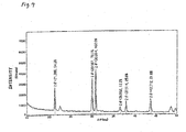
- an X-ray diffraction pattern necessary for specifying the crystal phase which contributes to light emission is disclosed.
- Equation 2 is one into which (equation 1) is changed.
- the plane spacing range of a reference diffraction peak is defined as 4.17 angstroms to 3.95 angstroms
- the range of the diffraction angle (2 ⁇ ) becomes 21.3° to 22.5° from (equation 2).
- the angle range R1 in which P1 appears is determined as follows.
- the start angle (R1s) and end angle (R1e) of the angle range R1 are derived from (equation 1) as follows: R 1 s : 2 ⁇ arcsin ⁇ ⁇ / ( 2 ⁇ d 0 ⁇ 0.720 ⁇ 1.015 ) ⁇ R 1 e : 2 ⁇ arcsin ⁇ ⁇ / ( 2 ⁇ d 0 ⁇ 0.720 ⁇ 0.985 ) ⁇
- the angle ranges in which P2, P3, P4 and P5 appear are defined as 0.698 time, 0.592 time, 0.572 time and 0.500 time, respectively, the plane spacing derived from the reference diffraction peak, and the deviation of the plane spacing associated with strain of the structure is taken as 1.5% without variation, the respective angle ranges become as follows: R 2 s : 2 ⁇ arcsin ⁇ sin ( ⁇ 0 ) / ( 0.698 ⁇ 1.015 ) ⁇ R 2 e : 2 ⁇ arcsin ⁇ sin ( ⁇ 0 ) / ( 0.698 ⁇ 0.985 ) ⁇ R 3 s : 2 ⁇ arcsin ⁇ sin ( ⁇ 0 ) / ( 0.592 ⁇ 1.015 ) ⁇ R 3 e : 2 ⁇ arcsin ⁇ sin ( ⁇ 0 ) / ( 0.592 ⁇ 0.985 ) ⁇ R 4 s : 2 ⁇ arcsin ⁇ sin (
- the presence of the specified crystal structure as defined in the present invention can be confirmed by confirming that the respective peaks from the reference peak P0 to P5 appear in the above-mentioned angle ranges.
- This crystal phase is a crystal phase different from merwinite described in non-patent document 1 and non-patent document 2.
- the above-mentioned angle ranges R1 to R5 are more preferably as follows in which the deviation of the plane spacing associated with strain of the structure is taken as 1.0% without variation.
- R 1 2 ⁇ arcsin ⁇ sin ( ⁇ 0 ) / ( 0.720 ⁇ 1.010 ) ⁇ to 2 ⁇ arcsin ⁇ sin ( ⁇ 0 ) / ( 0.720 ⁇ 0.990 ) ⁇
- R 2 2 ⁇ arcsin ⁇ sin ( ⁇ 0 ) / ( 0.698 ⁇ 1.010 ) ⁇ to 2 ⁇ arcsin ⁇ sin ( ⁇ 0 ) / ( 0.698 ⁇ 0.990 ) ⁇
- R 3 2 ⁇ arcsin ⁇ sin ( ⁇ 0 ) / ( 0.592 ⁇ 1.010 ) ⁇ to 2 ⁇ arcsin ⁇ sin ( ⁇ 0 ) / ( 0.592 ⁇ 0.990 ) ⁇
- R 4 2 ⁇ arcsin ⁇ sin ( ⁇ 0 ) / ( 0.572 ⁇ 1.010 ) ⁇ to 2 ⁇ arcsin ⁇ sin ( ⁇ 0 )
- the desired crystal phase can be obtained by using, for example, a raw material having a small particle size of 10 ⁇ m or less, particularly a raw material in which silica contains no water, allowing local aggregates not to exist before burning, which are considered to be uneven in composition, and performing burning under a reducing atmosphere using a crucible made of carbon.
- phosphors having high emission intensity which are obtained in the present invention contain the above-mentioned specified crystal phase. From this, it is true that they are a phosphor comprising a crystal phase of an alkali earth silicate containing at least one element selected from the group consisting of Ba, Sr, Ca and Mg, and a phosphor characterized by containing the above-mentioned specified crystal phase.
- a first light emitter which irradiates the above-mentioned phosphor with light emits light having a wavelength of 350 nm to 430 nm.
- a light emitter which emits light having the peak wavelength in the wavelength range of 350 nm to 430 nm.
- Specific examples of the first light emitters include a light emitting diode (LED), a laser diode (LD) and the like. In terms of low electric power consumption, a laser diode is more preferred. Above all, preferred is a GaN-based LED or LD using a GaN-based compound semiconductor.
- the GaN-based LED or LD is markedly high in emission output and external quantum efficiency, compared to a SiC-based LED or the like which emits light in this region, and extremely bright light emission is obtained at extremely low electric power by combination with the above-mentioned phosphor.
- the GaN-based LED or LD usually has an emission intensity of 100 times or more that of the SiC-based, for a current load of 20 mA.
- the GaN-based LED or LD one having an Al x Ga y N light emitting layer, a GaN light emitting layer or an In x Ga y N light emitting layer is preferred.
- the GaN-based LED of these, one having the In x Ga y N light emitting layer is particularly preferred because of its extremely high emission intensity.
- the GaN-based LD one having a multiple quantum well structure of the In x Ga y N layer and the GaN layer is particularly preferred because of its extremely high emission intensity.
- the value of X+Y is usually a value ranging from 0.8 to 1.2.
- the GaN-based LED one in which the light emitting layer is doped with Zn or Si or dopant-free one is preferred in terms of controlling emission characteristics.
- the GaN-based LED has the light emitting layer, a p layer, an n layer, electrodes and a substrate as basic constituent elements.
- One having a hetero structure in which the light emitting layer is sandwiched between the n type and p type Al x Ga y N layers, GaN layers, In x Ga y N layers or the like is preferred because of its high emission efficiency, and further, one in which the hetero structure is formed into a quantum well structure is more preferred because of its higher emission efficiency.
- a surface emitting type light emitter particularly a surface emitting type GaN-based laser diode, as the first light emitter, because it results in enhancement of emission efficiency of the whole light emitting device.
- the surface emitting type light emitter is a light emitter having strong light emission in the surface direction of a film.
- light emission in the surface direction of the light emitting layer can be made stronger than that in the edge direction by controlling the growth of crystals of the light emitting layer and the like and devising well a reflective layer and the like.
- the emission cross sectional area per unit emission amount can be increased by using the surface emitting type one, compared to the type of emitting light from the edges of the light emitting layer.
- the irradiation area can be extremely increased at the same amount of light to improve irradiation efficiency. Accordingly, stronger light emission can be obtained from the phosphor of the second light emitter.
- the second light emitter is preferably filmy.
- the light from the surface emitting type one has a sufficiently large cross sectional area, so that when the second light emitter is made filmy in its cross sectional direction, the cross sectional area of irradiation from the first light emitter to the phosphor increases per unit amount of the phosphor. Accordingly, the intensity of light emission from the phosphor can be more increased.
- the surface emitting type one is used as the first light emitter and the filmy one is used as the second light emitter, it is preferred to take a form in which the second filmy light emitter is directly brought into contact with a light emitting surface of the first light emitter.
- the term "contact” as used herein means to make a state in which the first light emitter and the second light emitter are in close contact with each other without the interposition of air or gas.
- FIG. 1 A schematic perspective view indicating positional relationship between a first light emitter and a second light emitter in one example of a light emitting device of the present invention is shown in Fig. 1.
- 1 designates a second filmy light emitter having the above-mentioned phosphor
- 2 designates a surface emitting type GaN-based LD as the first light emitter
- 3 designates a substrate.
- the LD 2 and the second light emitter 1 are each separately prepared, and surfaces thereof may be brought into contact with each other by an adhesive or another means, or the second light emitter may be formed as a film (molded) on a light emitting surface of the LD 2.
- the LD 2 and the second light emitter 1 can be put into a contact state.
- the light from the first light emitter and the light from the second light emitter are usually directed in all directions.
- a powder of the phosphor of the second light emitter is dispersed in a resin
- the light is partially reflected when the light goes out of the resin, thereby aligning the direction thereof to some degree. Accordingly, the light can be guided to the efficient direction to some degree, so that one in which the powder of the above-mentioned phosphor has been dispersed in the resin is preferably used.
- the phosphor is dispersed in the resin, the total irradiation area of the light from the first light emitter onto the second light emitter increases. It also has therefore the advantage of being able to increase emission intensity from the second light emitter.
- the resins which can be used in this case include various ones such as a silicon resin, an epoxy resin, a polyvinyl-based resin, a polyethylenic resin, a polypropylenic resin and a polyester-based resin.
- a silicon resin or an epoxy resin preferred is a silicon resin or an epoxy resin.
- the weight ratio of the powder of the second light emitter to the whole of the powder and the resin is usually from 10% to 95%, preferably from 20% to 90%, and more preferably from 30% to 80%.
- the phosphor is too much, emission efficiency decreases in some cases by aggregation of the powder.
- emission efficiency in turn decreases in some cases, because of absorption or scattering of the light by the resin.
- the light emitting device of the present invention comprises the above-mentioned phosphor as a wavelength conversion material and the light emitting element which emits light of 350 nm to 430 nm.
- the above-mentioned phosphor absorbs the light of 350 nm to 430 nm emitted by the light emitting element to provide the light emitting device which has good color rendering properties without depending on use environment and can emit high-intensity visible light.
- the phosphor having the crystal phase of the present invention emits light in a wavelength region indicating a red color or a white color by irradiation with light from the first light emitter which emits the light of 350 nm to 430 nm.
- the light emitting device of the present invention is suitable for a light emission source for a backlight source, a traffic signal or the like, an image display unit such as a color liquid crystal display, a lighting system such as surface light emission, or the like.
- Fig. 2 is a schematic cross sectional view showing one example of a light emitting device having a first light emitter (350 nm to 430nm light emitter) and a second light emitter, and 4 is the light emitting device, 5 is a mount lead, 6 is an inner lead, 7 is the first light emitter (light emitter of 350 nm to 430 nm), 8 is a phosphor-containing resin portion as the second light emitter, 9 is a conductive wire, and 10 is a mold member.
- a first light emitter 350 nm to 430nm light emitter
- 4 the light emitting device
- 5 is a mount lead
- 6 is an inner lead
- 7 is the first light emitter (light emitter of 350 nm to 430 nm)
- 8 is a phosphor-containing resin portion as the second light emitter
- 9 is a conductive wire
- 10 is a mold member.
- the light emitting device which is one example of the present invention has a general cannonball type form as shown in Fig. 2, and the first light emitter (350 nm to 430nm light emitter) 7 comprising a GaN-based light emitting diode and the like is fixed in an upper cup of the mount lead 5 by covering it with the phosphor-containing resin portion formed as the second light emitter by mixing and dispersing the phosphor in a binder such as a silicon resin, an epoxy resin or an acrylic resin, and pouring the dispersion into the cup.
- the first light emitter 7 and the mount lead 5, and the first light emitter 7 and the inner lead 6 are each conducted to each other with the conductive wire 9, and the whole thereof is covered and protected with the mold member 10 comprising an epoxy resin or the like.
- a surface emitting lighting system 11 in which this light emitting element 1 is incorporated, many light emitting devices 13 are disposed on a bottom surface of a square holding case 12 whose inner surface is made light-impermeable such as a white smooth surface, a power source, a circuit and the like (not shown) for driving the light emitting devices 13 are disposed in the outside thereof, and a diffuser panel 14 such as a milk-white acrylic plate is fixed to a portion corresponding to a lid of the holding case 12 for homogenization of light emission, as shown in Fig. 3.
- a diffuser panel 14 such as a milk-white acrylic plate is fixed to a portion corresponding to a lid of the holding case 12 for homogenization of light emission, as shown in Fig. 3.
- the surface emitting lighting system 11 is driven to apply voltage to the first light emitter of the light emitting element 13, thereby allowing light of 350 nm to 430 nm to be emitted.
- the light emission is partially absorbed by the above-mentioned phosphor in the phosphor-containing resin portion as the second light emitter to emit visible light.
- light emission having high color rendering properties is obtained by color mixing with blue light and the like which have not been absorbed by the phosphor. This light passes through the diffuser panel 14, and exits upward in the drawing. Thus, illuminating light having uniform brightness in a surface of the diffuser panel 14 of the holding case 12 is obtained.
- An aqueous solution of Ba(NO 3 ) 2 , an aqueous solution of Ca(NO 3 ) 2 ⁇ 4H 2 O, an aqueous solution of Eu (NO 3 ) 3 ⁇ 6H 2 O, an aqueous solution of Mn(NO 3 ) 2 ⁇ 6H 2 O and a suspension of colloidal silica (SiO 2 ) (the molar ratio of Ba (NO 3 ) 2 , Ca(NO 3 ) 2 ⁇ 4H 2 O, Eu (NO 3 ) 3 ⁇ 6H 2 O, Mn(NO 3 ) 2 ⁇ 6H 2 O and SiO 2 is 0.64:0.96:0.2:0.2:1) were mixed in a platinum container and dried.
- the mixture was burnt by heating under a stream of nitrogen gas containing 4% of hydrogen at 1050°C for 2 hours to produce a phosphor Ba 0.64 Ca 0.96 Eu 0.2 Mn 0.2 SiO 4 (phosphor used in a second light emitter).
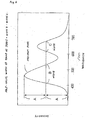
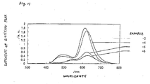
- the wavelength of an emission peak thereof, the intensity of the emission peak at the time when the intensity of an emission peak of Comparative Example A-2 described later is taken as 100 (hereinafter referred to as the relative intensity), and the half-value width are shown in Table 1.
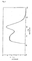
- This phosphor has a sufficiently wide half-value width, gives good color rendering properties, and emits a light red color having a peak wavelength within the range of 590 nm to 620 nm. This reveals that this phosphor emits reddish light which feels bright.
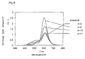
- a phosphor Ba 0.72 Ca 1.08 Eu 0.2 SiO 4 was produced in the same manner as in Example A-1 with the exception that an aqueous solution of Ba(NO 3 ) 2 , an aqueous solution of Ca(NO 3 ) 2 ⁇ 4H 2 O, an aqueous solution of Eu (NO 3 ) 3 ⁇ 6H 2 O and a suspension of colloidal silica (SiO 2 ) (the molar ratio of Ba(NO 3 ) 2 , Ca (NO 3 ) 2 ⁇ 4H 2 O, Eu(NO 3 ) 3 ⁇ 6H 2 O and SiO 2 is 0.72:1.08:0.2:1) were used as original solutions.
- a phosphor Ba 1.6 Eu 0.2 Mn 0.2 SiO 4 was produced in the same manner as in Example A-1 with the exception that an aqueous solution of Ba(NO 3 ) 2 , an aqueous solution of Eu(NO 3 ) 3 ⁇ 6H 2 O, an aqueous solution of Mn (NO 3 ) 2 ⁇ 6H 2 O and a suspension of colloidal silica (SiO 2 ) (the molar ratio of Ba(NO 3 ) 2 , Eu(NO 3 ) 3 ⁇ 6H 2 O, Mn(NO 3 ) 2 ⁇ 6H 2 O and SiO 2 is 1.6:0.2:0.2:1) were used as original solutions.
- a phosphor Ca 1.6 Eu 0.2 Mn 0.2 SiO 4 was produced in the same manner as in Example A-1 with the exception that an aqueous solution of Ca(NO 3 ) 2 ⁇ 4H 2 O, an aqueous solution of Eu (NO 3 ) 3 ⁇ 6H 2 O, an aqueous solution of Mn(NO 3 ) 2 ⁇ 6H 2 O and a suspension of colloidal silica (SiO 2 ) (the molar ratio of Ca(NO 3 ) 2 ⁇ 4H 2 O, Eu (NO 3 ) 3 ⁇ 6H 2 O, Mn (NO 3 ) 2 ⁇ 6H 2 O and SiO 2 is 1.6:0.2:0.2:1) were used as original solutions.
- a phosphor Ba 0.84 Ca 0.56 Eu 0.3 Mn 0.3 SiO 4 was produced in the same manner as in Example A-1 with the exception that an aqueous solution of Ba(NO 3 ) 2 , an aqueous solution of Ca (NO 3 ) 2 ⁇ 4H 2 O, an aqueous solution of Eu(NO 3 ) 3 ⁇ 6H 2 O, an aqueous solution of Mn(NO 3 ) 2 ⁇ 6H 2 O and a suspension of colloidal silica (SiO 2 ) (the molar ratio of Ba(NO 3 ) 2 , Ca (NO 3 ) 2 ⁇ 4H 2 O, Eu (NO 3 ) 3 ⁇ 6H 2 O, Mn(NO 3 ) 2 ⁇ 6H 2 O and SiO 2 is 0.84:0.56:0.3:0.3:1) were used as original solutions.
- a phosphor Ba 0.75 Ca 0.5 Eu 0.3 Mn 0.45 SiO 4 was produced in the same manner as in Example A-1 with the exception that an aqueous solution of Ba(NO 3 ) 2 , an aqueous solution of Ca(NO 3 ) 2 ⁇ 4H 2 O, an aqueous solution of Eu(NO 3 ) 3 ⁇ 6H 2 O, an aqueous solution of Mn(NO 3 ) 2 ⁇ 6H 2 O and a suspension of colloidal silica (SiO 2 ) (the molar ratio of Ba(NO 3 ) 2 , Ca (NO 3 ) 2 ⁇ 4H 2 O, Eu(NO 3 ) 3 ⁇ 6H 2 O, Mn(NO 3 ) 2 ⁇ 6H 2 O and SiO 2 is 0.75:0.5:0.3:0.45:1) were used as original solutions.
- a phosphor Ba 1.11 Ca 0.74 Eu 0.06 Mn 0.09 SiO 4 was produced in the same manner as in Example A-1 with the exception that an aqueous solution of Ba(NO 2 ) 2 , an aqueous solution of Ca(NO 3 ) 2 ⁇ 4H 2 O, an aqueous solution of Eu(NO 3 ) 3 ⁇ 6H 2 O, an aqueous solution of Mn(NO 3 ) 2 ⁇ 6H 2 O and a suspension of colloidal silica (SiO 2 ) (the molar ratio of Ba(NO 3 ) 2 , Ca (NO 3 ) 2 ⁇ 4H 2 O, Eu(NO 3 ) 3 ⁇ 6H 2 O, Mn(NO 3 ) 2 ⁇ 6H 2 O and SiO 2 is 1.11:0.74:0.06:0.09:1) were used as original solutions.
- An emission spectrum thereof is shown in Fig. 5.
- the x and y values of chromaticity coordinates indicating colors, the wavelength of the maximum peak, the intensity of the maximum peak of this phosphor at the time when the intensity of the maximum peak of a phosphor in Comparative Example A-5 described later is taken as 100 (hereinafter referred to as the relative intensity of the maximum peak), the ratio of the intensity at 600 nm to the intensity of the maximum peak, which gives an indication of to what extent a red component exists, and the half-value width of a group of peaks are shown in Table 2. This reveals that white light emission is obtained in which blue, green and red components all sufficiently exist, the spectrum width is very wide, and color rendering properties are high.
- the maximum peak means a peak which is highest in intensity when a plurality of peaks exist in an emission spectrum, and in the case of a single peak, the maximum peak means itself.
- the half-value width of a group of peaks gives an indication of how wide an emission spectrum distributes, and how high color rendering properties are, and is defined as the total of widths of wavelength regions having an intensity of half or more the intensity of the maximum peak in the spectrum, as shown in Fig. 6. For example, in Fig. 6, the half-value width of a group of peaks becomes the total of width B and width C.
- a phosphor Ba 0.68 Ca 1.02 Eu 0.2 Mn 0.1 SiO 4 was produced in the same manner as in Example A-1 with the exception that an aqueous solution of Ba(NO 3 ) 2 , an aqueous solution of Ca (NO 3 ) 2 ⁇ 4H 2 O, an aqueous solution of Eu(NO 3 ) 3 ⁇ 6H 2 O, an aqueous solution of Mn(NO 3 ) 2 ⁇ 6H 2 O and a suspension of colloidal silica (SiO 2 ) (the molar ratio of Ba(NO 3 ) 2 , Ca (NO 3 ) 2 ⁇ 4H 2 O, Eu(NO 3 ) 3 ⁇ 6H 2 O, Mn(NO 3 ) 2 ⁇ 6H 2 O and SiO 2 is 0.68:1.02:0.2:0.1:1) were used as original solutions.
- a phosphor Ba 0.72 Ca 1.08 Eu 0.2 SiO 4 was produced in the same manner as in Example A-1 with the exception that an aqueous solution of Ba(NO 3 ) 2 , an aqueous solution of Ca(NO 3 ) 2 ⁇ 4H 2 O, an aqueous solution of Eu(NO 3 ) 3 ⁇ 6H 2 O and a suspension of colloidal silica (SiO 2 ) (the molar ratio of Ba(NO 3 ) 2 , Ca(NO 3 ) 2 ⁇ 4H 2 O, Eu(NO 3 ) 3 ⁇ 6H 2 O and SiO 2 is 0.72:1.08:0.2:1) were used as original solutions.
- a phosphor Ba 1.7 Eu 0.2 Mn 0.1 SiO 4 was produced in the same manner as in Example A-1 with the exception that an aqueous solution of Ba(NO 3 ) 2 , an aqueous solution of Eu (NO 3 ) 3 ⁇ 6H 2 O, an aqueous solution of Mn(NO 3 ) 2 ⁇ 6H 2 O and a suspension of colloidal silica (SiO 2 ) (the molar ratio of Ba(NO 3 ) 2 , Eu(NO 3 ) 3 ⁇ 6H 2 O, Mn(NO 3 ) 2 ⁇ 6H 2 O and SiO 2 is 1.7:0.2:0.1:1) were used as original solutions.
- a phosphor Ca 1.7 Eu 0.2 Mn 0.1 SiO 4 was produced in the same manner as in Example A-1 with the exception that an aqueous solution of Ca (NO 3 ) 2 ⁇ 4H 2 O, an aqueous solution of Eu (NO 3 ) 3 ⁇ 6H 2 O, an aqueous solution of Mn(NO 3 ) 2 ⁇ 6H 2 O and a suspension of colloidal silica (SiO 2 ) (the molar ratio of Ca(NO 3 ) 2 ⁇ 4H 2 O, Eu(NO 3 ) 3 ⁇ 6H 2 O, Mn(NO 3 ) 2 ⁇ 6H 2 O and SiO 2 is 1.7:0.2:0.1:1) were used as original solutions.
- a phosphor Ba 0.93 Ca 0.62 Eu 0.3 Mn 0.15 SiO 4 was produced in the same manner as in Example A-1 with the exception that an aqueous solution of Ba(NO 3 ) 2 , an aqueous solution of Ca (NO 3 ) 2 ⁇ 4H 2 O, an aqueous solution of Eu(NO 3 ) 3 ⁇ 6H 2 O, an aqueous solution of Mn(NO 3 ) 2 ⁇ 6H 2 O and a suspension of colloidal silica (SiO 2 ) (the molar ratio of Ba (NO 3 ) 2 , Ca (NO 3 ) 2 ⁇ 4H 2 O, Eu(NO 3 ) 3 ⁇ 6H 2 O, Mn(NO 3 ) 2 ⁇ 6H 2 O and SiO 2 is 0.93:0.62:0.3:0.15:1) were used as original solutions.
- a phosphor Ba 1.133 Ca 0.378 Zn 0.189 Eu 0.2 Mn 0.1 SiO 4 was produced in the same manner as in Example A-1 with the exception that an aqueous solution of Ba(NO 3 ) 2 , an aqueous solution of Ca (NO 3 ) 2 ⁇ 4H 2 O, an aqueous solution of Zn(NO 3 ) 2 ⁇ 6H 2 O, an aqueous solution of Eu(NO 3 ) 3 -6H 2 O, an aqueous solution of Mn(NO 3 ) 2 ⁇ 6H 2 O and a suspension of colloidal silica (SiO 2 ) (the molar ratio of Ba(NO 3 ) 2 , Ca(NO 3 ) 2 ⁇ 4H 2 O, Zn(NO 3 ) 2 ⁇ 6H 2 O, Eu(NO 3 ) 3 ⁇ 6H 2 O, Mn(NO 3 ) 2 ⁇ 6H 2 O and SiO 2 is 1.133:0.378:0.189:0.2:0.1:1) were used as original solutions
- Example A-7 Ba 1.133 Ca 0.378 Zn 0.169 Eu 0.2 Mn 0.1 SiO 4 0.363 0.37 59B 60 1 193 0.1 0.25 Comparative Example A-4 Ba 0.72 Ca 1.
- BaCO 3 , CaCO 3 , Eu 2 O 3 , MnCO 3 ⁇ nH 2 O and SiO 2 were weighed to a molar ratio of 1.08:0.72:0.075:0.05:1, and NH 4 Cl was added as a flux, followed by mixing in a ball mill for 1 hour.
- This prepared powder was put in an alumina crucible, further put together with this crucible in a crucible made of carbon, and heated under a stream of nitrogen gas containing 4% of hydrogen at 1200°C for 6 hours, thereby producing a phosphor Ba 1.08 Ca 0.72 Eu 0.15 Mn 0.05 SiO 4 .
- X-ray diffraction measurement of this phosphor was made under the following conditions.
- the divergence angle of a divergence slit was adjusted so that the irradiation width of the X-ray did not exceed the width of the sample in measurement, and for the diffraction peak position (peak top) and diffraction intensity (height), values of the results of measurement in a stationary slit mode was read.
- the results of X-ray diffraction measurement are shown in Fig. 7.
- Table 3 shows that the obtained phosphor meets the conditions described in claim 6, and it was confirmed that the specified phase described above was contained.
- the x and y values of chromaticity coordinates, wavelength of emission peak and intensity of emission peak of this phosphor are shown in Table 4.
- a phosphor Ba 1.35 Ca 0.45 Eu 0.15 Mn 0.05 SiO 4 was obtained in the same manner as in Example A-8 with the exception that BaCO 3 , CaCO 3 , Eu 2 O 3 , MnCO 3 -nH 2 O and SiO 2 were weighed to a molar ratio of 1.35:0.45:0.075:0.05:1.
- the results of X-ray diffraction measurement are shown in Table 3, and this example meets the conditions of claim 6.
- An emission spectrum is shown in Fig. 8, and characteristics are summarized in Table 4.
- a phosphor Ba 1.20 Ca 0.4 Sr 0.2 Eu 0.15 Mn 0.05 SiO 4 was obtained in the same manner as in Example A-8 with the exception that BaCO 3 , CaCO 3 , SrCO 3 , Eu 2 O 3 , MnCO 3 ⁇ nH 2 O and SiO 2 were weighed to a molar ratio of 1.20:0.4:0.2:0.075:0.05:1.
- the results of X-ray diffraction measurement are shown in Table 3, and this example meets the conditions of claim 6.
- An emission spectrum is shown in Fig. 8, and characteristics are summarized in Table 4.
- a phosphor Ba 1.08 Ca 0.36 Sr 0.36 Eu 0.15 Mn 0.05 SiO 4 was obtained in the same manner as in Example A-8 with the exception that BaCO 3 , CaCO 3 , SrCO 3 , Eu 2 O 3 , MnCO 3 ⁇ nH 2 O and SiO 2 were weighed to a molar ratio of 1.08:0.36:0.36:0.075:0.05:1.
- the results of X-ray diffraction measurement are shown in Table 3, and this example meets the conditions of claim 6.
- An emission spectrum is shown in Fig. 8, and characteristics are summarized in Table 4.
- the mixture was burnt by heating under a stream of nitrogen gas containing 4% of hydrogen at 1050°c for 2 hours to produce a phosphor Ba 1.133 Ca 0.378 Mg 0.189 Eu 0.2 Mn 0.1 SiO 4 (phosphor used in a second light emitter).
- the wavelength of an emission peak thereof, the intensity of the emission peak at the time when the intensity of an emission peak of Comparative Example B-3 described later is taken as 100 (hereinafter referred to as the relative intensity), and the half-value width are shown in Table 5.
- This phosphor has a sufficiently wide half-value width, gives good color rendering properties, and emits a light red color having a peak wavelength within the range of 590 nm to 620 nm. This reveals that this phosphor emits reddish light which feels bright.
- a phosphor Ba 1.2 Ca 0.4 Mg 0.2 EU 0.2 SiO 4 was produced in the same manner as in Example B-1 with the exception that an aqueous solution of Ba(NO 3 ) 2 , an aqueous solution of Ca(NO 3 ) 2 ⁇ 4H 2 O, an aqueous solution of Mg(NO 3 ) 2 ⁇ 6H 2 O, an aqueous solution of Eu(NO 3 ) 3 ⁇ 6H 2 O and a suspension of colloidal silica (SiO 2 ) (the molar ratio of Ba(NO 3 ) 2 , Ca(NO 3 ) 2 ⁇ 4H 2 O, Mg(NO 3 ) 2 ⁇ 6H 2 O, Eu(NO 3 ) 3 ⁇ 6H 2 O and SiO 2 is 1.2:0.4:0.2:0.2:1) were used as original solutions.
- a phosphor Ba 0.72 Ca 1.08 Eu 0.2 SiO 4 was produced in the same manner as in Example B-1 with the exception that an aqueous solution of Ba(NO 3 ) 2 , an aqueous solution of Ca(NO 3 ) 2 ⁇ 4H 2 O, an aqueous solution of Eu (NO 3 ) 3 ⁇ 6H 2 O and a suspension of colloidal silica (SiO 2 ) (the molar ratio of Ba(NO 3 ) 2 , Ca(NO 2 ) 2 ⁇ 4H 2 O. Eu(NO 3 ) 3 ⁇ 6H 2 O and SiO 2 is 0.72:1.08:0.2:1) were used as original solutions.
- a phosphor Ba 1.6 Eu 0.2 Mn 0.2 SiO 4 was produced in the same manner as in Example B-1 with the exception that an aqueous solution of Ba(NO 3 ) 2 , an aqueous solution of Eu(NO 3 ) 3 ⁇ 6H 2 O, an aqueous solution of Mn (NO 3 ) 2 ⁇ 6H 2 O and a suspension of colloidal silica (SiO 2 ) (the molar ratio of Ba(NO 3 ) 2 , Eu(NO 3 ) 3 ⁇ 6H 2 O, Mn(NO 3 ) 2 ⁇ 6H 2 O and SiO 2 is 1.6:0.2:0,2:1) were used as original solutions.
- a phosphor Ca 1.6 Eu 0.2 Mn 0.2 SiO 4 was produced in the same manner as in Example B-1 with the exception that an aqueous solution of Ca(NO 3 ) 2 ⁇ 4H 2 O, an aqueous solution of Eu (NO 3 ) 3 ⁇ 6H 2 O, an aqueous solution of Mn(NO 3 ) 2 ⁇ 6H 2 O and a suspension of colloidal silica (SiO 2 ) (the molar ratio of Ca(NO 3 ) 2 ⁇ 4H 2 O, Eu(NO 3 ) 3 ⁇ 6H 2 O, Mn(NO 3 ) 2 ⁇ 6H 2 O and SiO 2 is 1.6:0.2:0.2:1) were used as original solutions.
- a phosphor Ba 0.587 Mg 1.173 Eu 0.2 Mn 0.04 SiO 4 was produced in the same manner as in Example B-1 with the exception that an aqueous solution of Ba(NO 3 ) 2 , an aqueous solution of Mg (NO 3 ) 2 ⁇ 6H 2 O, an aqueous solution of Eu(NO 3 ) 3 ⁇ 6H 2 O, an aqueous solution of Mn(NO 3 ) 2 ⁇ 6H 2 O and a suspension of colloidal silica (SiO 2 ) (the molar ratio of Ba(NO 3 ) 2 , Mg(NO 3 ) 2 ⁇ 6H 2 O, Eu(NO 3 ) 3 .6H 2 O, Mn(NO 3 ) 2 ⁇ 6H 2 O and SiO 2 is 0.587:1.173:0.2:0.04:1) were used as original solutions.
- Example B-1 Ba 1.133 Ca 0.378 Mg 0.189 Eu 0.2 Mn 0.1 SiO 4 602 147 73 0.1 0.11 0.25 Comparative Example B-1 Ba 1.2 Ca 0.4 Mg 0.2 Eu 0.2 SiO 4 496 183 122 0 0.11 0.25 Comparative Example B-2 Ba 0.72 Ca 1.08 Eu 0.2 SiO 4 448 99 104 0 0 0.60 Comparative Example B-3 Ba 1.6 Eu 0.2 Mn 0.2 SiO 4 509 100 62 0.2 0 0.00 Comparative Example B-4 Ca 1.8 Eu 0.2 Mn 0.2 Si
- a phosphor Ba 1.173 Ca 0.391 Mg 0.196 Eu 0.2 Mn 0.04 SiO 4 was produced in the same manner as in Example B-1 with the exception that an aqueous solution of Ba(NO 3 ) 2 , an aqueous solution of Ca (NO 3 ) 2 ⁇ 4H 2 O, an aqueous solution of Mg(NO 3 ) 2 ⁇ 6H 2 O, an aqueous solution of Eu(NO 3 ) 3 ⁇ 6H 2 O, an aqueous solution of Mn(NO 3 ) 2 ⁇ 6H 2 O and a suspension of colloidal silica (SiO 2 ) (the molar ratio of Ba(NO 3 ) 2 , Ca(NO 3 ) 2 ⁇ 4H 2 O, Mg(NO 3 ) 2 ⁇ 6H 2 O, Eu(NO 3 ) 3 ⁇ 6H 2 O, Mn(NO 3 ) 2 ⁇ 6H 2 O and SiO 2 is 1.173:0.391:0.196:0.2:0.04:1) were
- the maximum peak means a peak which is highest in intensity when a plurality of peaks exist in an emission spectrum and in the case of a single peak, the maximum peak means itself.
- the half-value width of a group of peaks gives an indication of how wide an emission spectrum distributes, and how high color rendering properties are, and is defined as the total of widths of wavelength regions having an intensity of half or more the intensity of the maximum peak in the spectrum, as shown in Fig. 6.
- a phosphor Ba 1.2 Ca 0.4 Mg 0.2 Eu 0.2 SiO 4 was produced in the same manner as in Example B-1 with the exception that an aqueous solution of Ba(NO 3 ) 2 , an aqueous solution of Ca(NO 3 ) 2 ⁇ 4H 2 O, an aqueous solution of Mg(NO 3 ) 2 ⁇ 6H 2 O, an aqueous solution of Eu(NO 3 ) 3 ⁇ 6H 2 O and a suspension of colloidal silica (SiO 2 ) (the molar ratio of Ba(NO 3 ) 2 , Ca (NO 3 ) 2 ⁇ 4H 2 O, Mg(NO 3 ) 2 ⁇ 6H 2 O, Eu(NO 3 ) 3 ⁇ 6H 2 O and SiO 2 is 1.2:0.4:0.2:0.2:1) were used as original solutions.
- a phosphor Ba 0.72 Ca 1.08 Eu 0.2 SiO 4 was produced in the same manner as in Example B-1 with the exception that an aqueous solution of Ba(NO 3 ) 2 , an aqueous solution of Ca(NO 3 ) 2 ⁇ 4H 2 O, an aqueous solution of Eu(NO 3 ) 3 ⁇ 6H 2 O and a suspension of colloidal silica (SiO 2 ) (the molar ratio of Ba(NO 3 ) 2 , Ca(NO 3 ) 2 ⁇ 4H 2 O, Eu(NO 3 ) 3 ⁇ 6H 2 O and SiO 2 is 0.72:1.08:0.2:1) were used as original solutions.
- a phosphor Ba 0.587 Mg 1.173 Eu 0.2 Mn 0.04 SiO 4 was produced in the same manner as in Example B-1 with the exception that an aqueous solution of Ba(NO 3 ) 2 , an aqueous solution of Mg(NO 3 ) 2 ⁇ 6H 2 O, an aqueous solution of Eu(NO 3 ) 3 ⁇ 6H 2 O, an aqueous solution of Mn(NO 3 ) 2 ⁇ 6H 2 O and a suspension of colloidal silica (SiO 2 ) (the molar ratio of Ba(NO 3 ) 2 , Mg(NO 3 ) 2 ⁇ 6H 2 O, Eu(NO 3 ) 3 ⁇ 6H 2 O, Mn(NO 3 ) 2 ⁇ 6H 2 O and SiO 2 is 0.587:1.173:0.2:0.04:1) were used as original solutions.
- BaCO 3 , CaCO 3 , MgCO 3 , Eu 2 O 3 , MnCO 3 ⁇ nH 2 O and SiO 2 were weighed to a molar ratio of 1.283:0.428:0.09:0.075:0.05:1, and NH 4 Cl was added as a flux, followed by mixing in a ball mill for 1 hour.
- This prepared powder was put in an alumina crucible, further put together with this crucible in a crucible made of carbon, and heated under a stream of nitrogen gas containing 4% of hydrogen at 1200°C for 6 hours, thereby producing a phosphor Ba 1.283 Ca 0.428 Mg 0.09 Eu 0.15 Mn 0.05 SiO 4 .
- the divergence angle of a divergence slit was adjusted so that the irradiation width of the X-ray did not exceed the width of the sample in measurement, and for the diffraction peak position (peak top) and diffraction intensity (height), values of the results of measurement in a stationary slit mode was read.
- the results of X-ray diffraction measurement are shown in Fig. 10.
- Table 7 shows that the obtained phosphor meets the conditions described in claim 6, and it was confirmed that the specified phase described above was contained.
- the x and y values of chromaticity coordinates, wavelength of emission peak and intensity of emission peak of this phosphor are shown in Table 8.
- a phosphor Ba 1.215 Ca 0.405 Mg 0.16 Eu 0.15 Mn 0.05 SiO 4 was obtained in the same manner as in Example B-3 with the exception that BaCO 3 , CaCO 3 , MgCO 3 , Eu 2 O 3 , MnCO 3 ⁇ nH 2 O and SiO 2 were weighed to a molar ratio of 1.215:0.405:0.180:0.075:0.05:1.
- the results of X-ray diffraction measurement are shown in Table 7, and this example meets the conditions of claim 6.
- An emission spectrum is shown in Fig. 11, and characteristics are summarized in Table 8.
- a phosphor Ba 0.855 Ca 0.285 Sr 0.57 Mg 0.09 Eu 0.15 Mn 0.05 SiO 4 was obtained in the same manner as in Example B-3 with the exception that BaCO 3 , CaCO 3 , SrCO 3 , MgCO 3 , Eu 2 O 3 , MnCO 3 ⁇ nH 2 O and SiO 2 were weighed to a molar ratio of 0.855:0.285:0.57:0.09:0.075:0.05:1.
- the results of X-ray diffraction measurement are shown in Table 7, and this example meets the conditions of claim 6.
- An emission spectrum is shown in Fig. 11, and characteristics are summarized in Table 8.
- a phosphor Ba 0.81 Ca 0.27 Sr 0.54 Mg 0.18 Eu 0.15 Mn 0.05 SiO 4 was obtained in the same manner as in Example B-3 with the exception that BaCO 3 , CaCO 3 , SrCO 3 , MgCO 3 , Eu 2 O 3 , MnCO 3 ⁇ nH 2 O and SiO 2 were weighed to a molar ratio of 0.810:0.27:0.54:0.18: 0.075:0.05:1.
- the results of X-ray diffraction measurement are shown in Table 7, and this example does not meet the conditions of claim 6.
- An emission spectrum is shown in Fig. 11, and characteristics are summarized in Table 8.
- Example B-3 Reference Diffraction Peak Angle Angle Range Start Angle End Angle Measured Angle Measured Relative Intensity 21.512 R1 29.741 30.356 30.222 88.0 intensity R2 30.701 31.337 31.106 100.0 67.5 R3 36.375 37.136 36.723 17.0 R4 37.694 38.485 38.207 35.9 R5 43.377 44.299 44.006 43.6
- Example B-4 Reference Diffraction Peak Angle Angle Range Start Angle End Angle Measured Angle Measured Relative Intensity 21.761 R1 30.089 30.712 30.523 94.0 intensity R2 31.061 31.705 31.396 100.0 70.1 R3 36.806 37.577 37.049 18.7 R4 38.141 38.943 38.528 32.4 R5 43.898 44.833 44.346 41.1
- Example B-5 Reference Diffraction Peak Angle Angle Range Start Angle End Angle Measured Angle Measured Relative Intensity 21.834 R1 30.191 30.816 30.641 72.8 Intensity R
- An aqueous solution of Ba(NO 3 ) 2 , an aqueous solution of Mg(NO 3 ) 2 ⁇ 6H 2 O, an aqueous solution of Eu(NO 3 ) 3 ⁇ 6H 2 O, an aqueous solution of Mn(NO 3 ) 2 ⁇ 6H 2 O and a suspension of colloidal silica (SiO 2 ) (the molar ratio of Ba(NO 3 ) 2 , Mg(NO 3 ) 2 ⁇ 6H 2 O, Eu(NO 3 ) 3 ⁇ 6H 2 O, Ma(NO 3 ) 2 ⁇ 6H 2 O and SiOz is 0.935:0.935:0.1:0.03:1) were mixed in a platinum container and dried.
- the mixture was burnt by heating under a stream of nitrogen gas containing 4% of hydrogen at 1050°C for 2 hours to produce a phosphor Ba 0.935 Mg 0.935 Eu 0.1 Mn 0.03 SiO 4 (phosphor used in a second light emitter) .
- the wavelength of an emission peak thereof, the intensity of the emission peak at the time when the intensity of an emission peak of Comparative Example C-5 described later is taken as 100 (hereinafter referred to as the relative intensity), and the half-value width are shown in Table 9.
- this phosphor emits strong red light giving high color rendering properties because of its sufficiently high intensity and wide half-value width, and that it emits bright deep red light, because the wavelength of emission peak is in the region of 615 nm to 645 nm.
- relative intensities at excitation wavelengths of 254 nm, 280 nm, 382 nm and 400 nm are 208, 328, 351 and 320, respectively, and light emission by excitation at around 400 nm is strong 1.5 times or more the conventional light emission by excitation at 254 nm.
- this phosphor is a phosphor which is very advantageous to a light source of a GaN-based semiconductor.
- a phosphor Ba 0.95 Mg 0.95 EU 0.1 SiO 4 was produced in the same manner as in Example C-1 with the exception that an aqueous solution of Ba(NO 3 ) 2 , an aqueous solution of Mg(NO 3 ) 2 ⁇ 6H 2 O, an aqueous solution of Eu(NO 3 ) 3 ⁇ 6H 2 O and a suspension of colloidal silica (SiO 2 ) (the molar ratio of Ba(NO 3 ) 2 , Mg(NO 3 ) 2 ⁇ 6H 2 O, Eu(NO 3 ) 3 ⁇ 6H 2 O and SiO 2 is 0.95:0.95:0.1:1) were used as original solutions.
- a phosphor Ba 0.623 Mg 1.247 Eu 0.1 Mn 0.03 SiO 4 was produced in the same manner as in Example C-1 with the exception that an aqueous solution of Ba(NO 3 ) 2 , an aqueous solution of Mg (NO 3 ) 2 ⁇ 6H 2 O, an aqueous solution of Eu(NO 3 ) 3 ⁇ 6H 2 O, an aqueous solution of Mn(NO 3 ) 2 ⁇ 6H 2 O and a suspension of colloidal silica (SiO 2 ) (the molar ratio of Ba(NO 3 ) 2 , Mg (NO 3 ) 2 ⁇ 6H 2 O, Eu(NO 3 ) 3 ⁇ 6H 2 O, Mn(NO 3 ) 2 ⁇ 6H 2 O and SiO 2 is 0.623:1.247:0.1:0.03:1) were used as original solutions.
- a phosphor Ba 0.633 Mg 1.267 Eu 0.1 SiO 4 was produced in the same manner as in Example C-1 with the exception that an aqueous solution of Ba(NO 3 ) 2 , an aqueous solution of Mg(NO 3 ) 2 ⁇ 6H 2 O, an aqueous solution of Eu(NO 3 ) 3 ⁇ 6H 2 O and a suspension of colloidal silica (SiO 2 ) (the molar ratio of Ba(NO 3 ) 2 , Mg(NO 3 ) 2 ⁇ 6H 2 O, Eu(NO 3 ) 3 ⁇ 6H 2 O and SiO 2 is 0.633:1.267:0.1:1) were used as original solutions.
- a phosphor Ba 0.587 Mg 1.173 Eu 0.2 Mn 0.04 SiO 4 was produced in the same manner as in Example C-1 with the exception that an aqueous solution of Ba(NO 3 ) 2 , an aqueous solution of Mg(NO 3 ) 2 ⁇ 6H 2 O, an aqueous solution of Eu(NO 3 ) 3 ⁇ 6H 2 O, an aqueous solution of Mn(NO 3 ) 2 ⁇ 6H 2 O and a suspension of colloidal silica (SiO 2 ) (the molar ratio of Ba(NO 3 ) 2 , Mg (NO 3 ) 2 ⁇ 6H 2 O, Eu (NO 3 ) 3 ⁇ 6H 2 O, Mn(NO 3 ) 2 ⁇ 6H 2 O and SiO 2 is 0.587:1.173:0.2:0.04:1) were used as original solutions.
- a phosphor Ba 0.6 Mg 1.2 Eu 0.2 SiO 4 was produced in the same manner as in Example C-1 with the exception that an aqueous solution of Ba(NO 3 ) 2 , an aqueous solution of Mg(NO 3 ) 2 ⁇ 6H 2 O, an aqueous solution of Eu(NO 3 ) 3 ⁇ 6H 2 O and a suspension of colloidal silica (SiO 2 ) (the molar ratio of Ba(NO 3 ) 2 , Mg(NO 3 ) 2 ⁇ 6H 2 O, Eu(NO 3 ) 3 ⁇ 6H 2 O and SiO 2 is 0.6:1.2:0.2:1) were used as original solutions.
- a phosphor Ba 1.7 Eu 0.2 Mn 0.1 SiO 4 was produced in the same manner as in Example C-1 with the exception that an aqueous solution of Ba(NO 3 ) 2 , an aqueous solution of Eu(NO 3 ) 3 ⁇ 6H 2 O, an aqueous solution of Mn (NO 3 ) 2 ⁇ 6H 2 O and a suspension of colloidal silica (SiO 2 ) (the molar ratio of Ba(NO 3 ) 2 , Eu(NO 3 ) 3 ⁇ 6H 2 O, Mn(NO 3 ) 2 and SiO 2 is 1.7:0.2:0.1:1) were used as original solutions.
- a phosphor Ba 0.567 Ca 0.567 Mg 0.566 Eu 0.2 Mn 0.1 SiO 4 was produced in the same manner as in Example C-1 with the exception that an aqueous solution of Ba(NO 3 ) 2 , an aqueous solution of Ca(NO 3 ) 2 ⁇ 4H 2 O, an aqueous solution of Mg(NO 3 ) 2 ⁇ 6H 2 O, an aqueous solution of Eu(NO 3 ) 3 ⁇ 6H 2 O, an aqueous solution of Mn (NO 3 ) 2 ⁇ 6H 2 O and a suspension of colloidal silica (SiO 2 ) (the molar ratio of Ba(NO 3 ) 2 , Ca(NO 3 ) 2 , Mg (NO 3 ) 2 ⁇ 6H 2 O, Eu (NO 3 ) 3 ⁇ 6H 2 O, Mn (NO 3 ) 2 ⁇ 6H 2 O and SiO 2 is 0.567:0.567:0.566:0.2:0.1:1) were used as original solutions.
- a phosphor Ba 0.92 Mg 0.92 Eu 0.1 Mn 0.06 SiO 4 was produced in the same manner as in Example C-1 with the exception that an aqueous solution of Ba(NO 3 ) 2 , an aqueous solution of Mg(NO 3 ) 2 ⁇ 6H 2 O, an aqueous solution of Eu(NO 3 ) 3 ⁇ 6H 2 O, an aqueous solution of Mn(NO 3 ) 2 ⁇ 6H 2 O and a suspension of colloidal silica (SiO 2 ) (the molar ratio of Ba(NO 3 ) 2 , Mg(NO 3 ) 2 ⁇ 6H 2 O, Eu(NO 3 ) 3 ⁇ 6H 2 O, Mn(NO 3 ) 2 ⁇ 6H 2 O and SiO 2 is 0.92:0.92:0.1:0.06:1) were used as original solutions.
- An emission spectrum thereof is shown in Fig. 13.
- the wavelength and relative intensity of a peak of 590 nm or more (a peak of a red component), the wavelength and relative intensity of the maximum peak of less than 590 nm, the half-value width of a group of peaks and the x and y values of chromaticity coordinates indicating colors are shown in Table 10. This shows that a wide spectrum containing a deep red component in which the peak wavelength is in the region of 615 nm to 645 nm and also containing blue and green components is obtained to give high color rendering properties, resulting in bright white light emission.
- the maximum peak of less than 590 nm means a peak which is highest in intensity when a plurality of peaks exist in the region of less than 590 run in an emission spectrum, and in the case of a single peak, the maximum peak means itself.
- the half-value width of a group of peaks gives an indication of how wide an emission spectrum distributes, and how high color rendering properties are, and is defined as the total of widths of wavelength regions having an intensity of half or more the intensity of the maximum peak in the spectrum, as shown in Fig. 6.
- a phosphor Ba 0.95 Mg 0.95 Eu 0.1 SiO 4 emitting white light was produced in the same manner as in Example C-1 with the exception that an aqueous solution of Ba(NO 3 ) 2 , an aqueous solution of Mg(NO 3 ) 2 ⁇ 6H 2 O, an aqueous solution of Eu(NO 3 ) 3 ⁇ 6H 2 O and a suspension of colloidal silica (SiO 2 ) (the molar ratio of Ba(NO 3 ) 2 , Mg(NO 3 ) 2 ⁇ 6H 2 O, Eu (NO 3 ) 3 ⁇ 6H 2 O and SiO 2 is 0.95:0.95:0.1:1) were used as original solutions.
- a phosphor Ba 1.2 Ca 0.2 Mg 0.4 Eu 0.2 SiO 4 was produced in the same manner as in Example C-1 with the exception that an aqueous solution of Ba(NO 3 ) 2 , an aqueous solution of Ca(NO 3 ) 2 ⁇ 4H 2 O, an aqueous solution of Mg(NO 3 ) 2 ⁇ 6H 2 O, an aqueous solution of Eu(NO 3 ) 3 ⁇ 6H 2 O and a suspension of colloidal silica (SiO 2 ) (the molar ratio of Ba(NO 3 ) 2 , Ca(NO 3 ) 2 ⁇ 4H 2 O, Mg(NO 3 ) 2 ⁇ 6H 2 O, Eu(NO 3 ) 3 ⁇ 6H 2 O and SiO 2 is 1.2:0.2:0.4:0.2:1) were used as original solutions.
- a phosphor Ba 0.82 Mg 0.82 Eu 0.3 Mn 0.06 SiO 4 was produced in the same manner as in Example C-1 with the exception that an aqueous solution of Ba(NO 3 ) 2 , an aqueous solution of Mg(NO 3 ) 2 ⁇ 6H 2 O, an aqueous solution of Eu(NO 3 ) 3 ⁇ 6H 2 O, an aqueous solution of Mn(NO 3 ) 2 ⁇ 6H 2 O and a suspension of colloidal silica (SiO 2 ) (the molar ratio of Ba(NO 3 ) 2 , Mg(NO 3 ) 2 ⁇ 6H 2 O, Eu(NO 3 ) 3 ⁇ 6H 2 O, Mn(NO 3 ) 2 ⁇ 6H 2 O and SiO 2 is 0.82:0.82:0.3:0.06:1) were used as original solutions.
- a phosphor Ba 0.85 Mg 0.85 Eu 0.3 SiO 4 was produced in the same manner as in Example C-1 with the exception that an aqueous solution of Ba(NO 3 ) 2 , an aqueous solution of Mg(NO 3 ) 2 ⁇ 6H 2 O, an aqueous solution of Eu (NO 3 ) 3 ⁇ 6H 2 O and a suspension of colloidal silica (SiO 2 ) (the molar ratio of Ba(NO 3 ) 2 , Mg(NO 3 ) 2 ⁇ 6H 2 O, Eu(NO 3 ) 3 ⁇ 6H 2 O and SiO 2 is 0.85:0.85:0.3:1) were used as original solutions.
- a phosphor Ba 0.88 Ca 0.44 Mg 0.44 Eu 0.2 Mn 0.04 SiO 4 was produced in the same manner as in Example C-1 with the exception that an aqueous solution of Ba(NO 3 ) 2 , an aqueous solution of Ca(NO 3 ) 2 ⁇ 4H 2 O, an aqueous solution of Mg(NO 3 ) 2 ⁇ 6H 2 O, an aqueous solution of Eu(NO 3 ) 3 ⁇ 6H 2 O, an aqueous solution of Mn(NO 3 ) 2 ⁇ 6H 2 O and a suspension of colloidal silica (SiO 2 ) (the molar ratio of Ba(NO 3 ) 2 , Ca(NO 3 ) 2 , Mg(NO 3 ) 2 ⁇ 6H 2 O, Eu(NO 3 ) 3 ⁇ 6H 2 O, Mn(NO 3 ) 2 ⁇ 6H 2 O and SiO 2 is 0.88:0.44:0.44:0.2:0.04:1) were used as original solutions.
- a phosphor Ba 1-144 Ca 0.216 Mg 0.48 Eu 0.01 Mn 0.15 SiO 4 was produced in the same manner as in Example C-1 with the exception that an aqueous solution of Ba(NO 3 ) 2 , an aqueous solution of Ca (NO 3 ) 2 ⁇ 4H 2 O, an aqueous solution of Mg (NO 3 ) 2 ⁇ 6H 2 O, an aqueous solution of Eu(NO 3 ) 3 ⁇ 6H 2 O, an aqueous solution of Mn (NO 3 ) 2 ⁇ 6H 2 O and a suspension of colloidal silica (SiO 2 ) (the molar ratio of Ba (NO 3 ) 2 , Ca(NO 3 ) 2 , Mg(NO 3 ) 2 ⁇ 6H 2 O, Eu (NO 3 ) 3 ⁇ 6H 2 O, Mn (NO 3 ) 2 ⁇ 6H 2 O and SiO 2 is 1.144:0.216:0.48:0.01:0.15:1) were used as original solutions.
- Patent Application No. 2004-9768 Patent Application No. 2004-9768
- Patent Application No. 2004-9769 Patent Application No. 2004-9769
- Patent Application No. 2004-9770 Patent Application No. 2004-9770
- a high-efficiency red light emitting phosphor and white phosphor for using in a display or lighting which high-efficiently emits light in combination with a light source which emits light in the region from near-ultraviolet light to visible light.
Landscapes
- Chemical & Material Sciences (AREA)
- Inorganic Chemistry (AREA)
- Engineering & Computer Science (AREA)
- Materials Engineering (AREA)
- Organic Chemistry (AREA)
- Physics & Mathematics (AREA)
- Condensed Matter Physics & Semiconductors (AREA)
- General Physics & Mathematics (AREA)
- Electromagnetism (AREA)
- Optics & Photonics (AREA)
- Luminescent Compositions (AREA)
- Devices For Indicating Variable Information By Combining Individual Elements (AREA)
- Vessels And Coating Films For Discharge Lamps (AREA)
Applications Claiming Priority (4)
| Application Number | Priority Date | Filing Date | Title |
|---|---|---|---|
| JP2004009770 | 2004-01-16 | ||
| JP2004009768 | 2004-01-16 | ||
| JP2004009769 | 2004-01-16 | ||
| PCT/JP2005/000726 WO2005068584A1 (ja) | 2004-01-16 | 2005-01-14 | 蛍光体、及びそれを用いた発光装置、照明装置ならびに画像表示装置 |
Publications (3)
| Publication Number | Publication Date |
|---|---|
| EP1715023A1 true EP1715023A1 (de) | 2006-10-25 |
| EP1715023A4 EP1715023A4 (de) | 2009-01-07 |
| EP1715023B1 EP1715023B1 (de) | 2012-10-24 |
Family
ID=34799322
Family Applications (1)
| Application Number | Title | Priority Date | Filing Date |
|---|---|---|---|
| EP05703954A Expired - Fee Related EP1715023B1 (de) | 2004-01-16 | 2005-01-14 | Leuchtstoff und ihn umfassende lichtemittierende vorrichtung, beleuchtungsvorrichtung und bildanzeige |
Country Status (3)
| Country | Link |
|---|---|
| US (1) | US7608200B2 (de) |
| EP (1) | EP1715023B1 (de) |
| WO (1) | WO2005068584A1 (de) |
Cited By (3)
| Publication number | Priority date | Publication date | Assignee | Title |
|---|---|---|---|---|
| WO2008122332A1 (de) | 2007-04-04 | 2008-10-16 | Merck Patent Gmbh | Verfahren zur herstellung von leuchtstoffen bestehend aus orthosilikaten für pcleds |
| WO2008149256A1 (en) * | 2007-06-05 | 2008-12-11 | Koninklijke Philips Electronics N.V. | Self-supporting luminescent film and phosphor-enhanced illumination system |
| DE102006016548B4 (de) | 2005-04-15 | 2021-10-07 | Osram Gmbh | Blau bis Gelb-Orange emittierender Leuchtstoff und Lichtquelle mit derartigem Leuchtstoff |
Families Citing this family (27)
| Publication number | Priority date | Publication date | Assignee | Title |
|---|---|---|---|---|
| FR2846663B1 (fr) * | 2002-11-05 | 2006-08-11 | Rhodia Elect & Catalysis | Materiau transformant la lumiere, notamment pour parois de serres, comprenant comme additif un silicate de baryum et de magnesium |
| KR100655894B1 (ko) * | 2004-05-06 | 2006-12-08 | 서울옵토디바이스주식회사 | 색온도 및 연색성이 우수한 파장변환 발광장치 |
| KR100658700B1 (ko) * | 2004-05-13 | 2006-12-15 | 서울옵토디바이스주식회사 | Rgb 발광소자와 형광체를 조합한 발광장치 |
| US8308980B2 (en) | 2004-06-10 | 2012-11-13 | Seoul Semiconductor Co., Ltd. | Light emitting device |
| KR100665299B1 (ko) | 2004-06-10 | 2007-01-04 | 서울반도체 주식회사 | 발광물질 |
| KR100665298B1 (ko) * | 2004-06-10 | 2007-01-04 | 서울반도체 주식회사 | 발광장치 |
| KR101142519B1 (ko) * | 2005-03-31 | 2012-05-08 | 서울반도체 주식회사 | 적색 형광체 및 녹색 형광체를 갖는 백색 발광다이오드를채택한 백라이트 패널 |
| TWI323947B (en) * | 2005-05-24 | 2010-04-21 | Seoul Semiconductor Co Ltd | Light emitting device and phosphor of alkaline earth sulfide therefor |
| KR100724591B1 (ko) * | 2005-09-30 | 2007-06-04 | 서울반도체 주식회사 | 발광 소자 및 이를 포함한 led 백라이트 |
| KR101258397B1 (ko) * | 2005-11-11 | 2013-04-30 | 서울반도체 주식회사 | 구리 알칼리토 실리케이트 혼성 결정 형광체 |
| KR101055772B1 (ko) * | 2005-12-15 | 2011-08-11 | 서울반도체 주식회사 | 발광장치 |
| JP5315616B2 (ja) * | 2006-02-10 | 2013-10-16 | 三菱化学株式会社 | 発光装置、バックライト用白色発光体、及び画像表示装置 |
| WO2007105845A1 (en) | 2006-03-16 | 2007-09-20 | Seoul Semiconductor Co., Ltd. | Fluorescent material and light emitting diode using the same |
| KR100875443B1 (ko) | 2006-03-31 | 2008-12-23 | 서울반도체 주식회사 | 발광 장치 |
| JP4188404B2 (ja) * | 2006-05-19 | 2008-11-26 | 三井金属鉱業株式会社 | 白色蛍光体および白色発光素子乃至装置 |
| KR101258227B1 (ko) | 2006-08-29 | 2013-04-25 | 서울반도체 주식회사 | 발광 소자 |
| JP4466757B2 (ja) * | 2007-04-18 | 2010-05-26 | 三菱化学株式会社 | 蛍光体、蛍光体含有組成物、発光装置、照明装置、画像表示装置、及び窒素含有化合物 |
| RU2467051C2 (ru) | 2007-08-22 | 2012-11-20 | Сеул Семикондактор Ко., Лтд. | Люминофоры на основе нестехиометрических тетрагональных силикатов меди и щелочноземельного металла и способ их получения |
| KR101055769B1 (ko) | 2007-08-28 | 2011-08-11 | 서울반도체 주식회사 | 비화학양론적 정방정계 알칼리 토류 실리케이트 형광체를채택한 발광 장치 |
| JP5330263B2 (ja) | 2007-12-07 | 2013-10-30 | 株式会社東芝 | 蛍光体およびそれを用いたled発光装置 |
| KR20100112445A (ko) * | 2009-04-09 | 2010-10-19 | 삼성전자주식회사 | 형광체 및 이를 포함하는 백색 발광 소자 |
| KR101055762B1 (ko) | 2009-09-01 | 2011-08-11 | 서울반도체 주식회사 | 옥시오소실리케이트 발광체를 갖는 발광 물질을 채택한 발광 장치 |
| DE102009030205A1 (de) * | 2009-06-24 | 2010-12-30 | Litec-Lp Gmbh | Leuchtstoffe mit Eu(II)-dotierten silikatischen Luminophore |
| KR101028329B1 (ko) * | 2010-04-28 | 2011-04-12 | 엘지이노텍 주식회사 | 발광 소자 패키지 및 그 제조방법 |
| CN102408890A (zh) * | 2011-11-15 | 2012-04-11 | 杭州广陵科技开发有限公司 | 一种硅酸盐绿色荧光粉及其制备方法 |
| WO2015044106A1 (en) * | 2013-09-26 | 2015-04-02 | Koninklijke Philips N.V. | New nitridoalumosilicate phosphor for solid state lighting |
| CN103965894B (zh) * | 2014-05-23 | 2016-02-24 | 四川大学 | 一种白光led用硅酸盐单基质白光荧光粉及其制备方法 |
Citations (3)
| Publication number | Priority date | Publication date | Assignee | Title |
|---|---|---|---|---|
| GB1199541A (en) * | 1968-03-15 | 1970-07-22 | Sylvania Electric Prod | Phosphor and Phosphor Coated Arc Discharge Device |
| US20020063301A1 (en) * | 2000-09-21 | 2002-05-30 | Tetsuya Hanamoto | Semiconductor light-emitting device and light-emitting display device therewith |
| EP1484803A1 (de) * | 2002-02-15 | 2004-12-08 | Mitsubishi Chemical Corporation | Lichtemissionsbauelement und beleuchtungseinrichtung damit |
Family Cites Families (24)
| Publication number | Priority date | Publication date | Assignee | Title |
|---|---|---|---|---|
| JPH08315820A (ja) * | 1995-05-11 | 1996-11-29 | Petoca:Kk | 二次電池負極材用炭素繊維及びその製造方法 |
| WO1997027267A1 (fr) * | 1996-01-22 | 1997-07-31 | Kasei Optonix, Ltd. | Phosphore pouvant etre stimule par la lumiere |
| CN1062581C (zh) | 1997-03-26 | 2001-02-28 | 肖志国 | 硅酸盐长余辉发光材料及其制造方法 |
| US6278135B1 (en) * | 1998-02-06 | 2001-08-21 | General Electric Company | Green-light emitting phosphors and light sources using the same |
| US6294800B1 (en) * | 1998-02-06 | 2001-09-25 | General Electric Company | Phosphors for white light generation from UV emitting diodes |
| US6099754A (en) * | 1998-03-31 | 2000-08-08 | Sarnoff Corporation | Long persistence red phosphors |
| US6429583B1 (en) | 1998-11-30 | 2002-08-06 | General Electric Company | Light emitting device with ba2mgsi2o7:eu2+, ba2sio4:eu2+, or (srxcay ba1-x-y)(a1zga1-z)2sr:eu2+phosphors |
| KR100306996B1 (ko) | 1999-09-04 | 2001-09-24 | 박호군 | 신규 램프용 규산염계 형광체 |
| US6466135B1 (en) * | 2000-05-15 | 2002-10-15 | General Electric Company | Phosphors for down converting ultraviolet light of LEDs to blue-green light |
| US6621211B1 (en) | 2000-05-15 | 2003-09-16 | General Electric Company | White light emitting phosphor blends for LED devices |
| JP2004505172A (ja) * | 2000-07-28 | 2004-02-19 | オスラム オプト セミコンダクターズ ゲゼルシャフト ミット ベシュレンクテル ハフツング | 波長変換のためのルミネセンス変換ベースの発光ダイオード及び蛍光体 |
| DE10036940A1 (de) * | 2000-07-28 | 2002-02-07 | Patent Treuhand Ges Fuer Elektrische Gluehlampen Mbh | Lumineszenz-Konversions-LED |
| JP3985478B2 (ja) | 2000-09-29 | 2007-10-03 | 住友化学株式会社 | 真空紫外線励起発光素子用の蛍光体 |
| JP4023222B2 (ja) * | 2002-05-31 | 2007-12-19 | 住友化学株式会社 | ケイ酸塩蛍光体の製造方法 |
| JP4168776B2 (ja) | 2002-02-15 | 2008-10-22 | 三菱化学株式会社 | 発光装置及びそれを用いた照明装置 |
| JP2003261868A (ja) * | 2002-03-08 | 2003-09-19 | National Institute Of Advanced Industrial & Technology | ケイ酸塩蛍光体の製造方法 |
| JP2003313549A (ja) * | 2002-04-24 | 2003-11-06 | Sumitomo Chem Co Ltd | 蛍光体 |
| JP2004009770A (ja) | 2002-06-03 | 2004-01-15 | Jintaro Nakade | 電動アシスト人力車 |
| JP4138369B2 (ja) | 2002-06-03 | 2008-08-27 | 本田技研工業株式会社 | 可撓長尺部品支持構造 |
| JP2004009768A (ja) | 2002-06-03 | 2004-01-15 | Inoac Corp | ソリッドタイヤ |
| DE10259946A1 (de) * | 2002-12-20 | 2004-07-15 | Tews, Walter, Dipl.-Chem. Dr.rer.nat.habil. | Leuchtstoffe zur Konversion der ultravioletten oder blauen Emission eines lichtemittierenden Elementes in sichtbare weiße Strahlung mit sehr hoher Farbwiedergabe |
| US6982045B2 (en) * | 2003-05-17 | 2006-01-03 | Phosphortech Corporation | Light emitting device having silicate fluorescent phosphor |
| US7026755B2 (en) * | 2003-08-07 | 2006-04-11 | General Electric Company | Deep red phosphor for general illumination applications |
| US7077979B2 (en) * | 2003-10-10 | 2006-07-18 | The Regents Of The University Of California | Red phosphors for solid state lighting |
-
2005
- 2005-01-14 EP EP05703954A patent/EP1715023B1/de not_active Expired - Fee Related
- 2005-01-14 WO PCT/JP2005/000726 patent/WO2005068584A1/ja active Application Filing
- 2005-01-14 US US10/586,397 patent/US7608200B2/en not_active Expired - Fee Related
Patent Citations (3)
| Publication number | Priority date | Publication date | Assignee | Title |
|---|---|---|---|---|
| GB1199541A (en) * | 1968-03-15 | 1970-07-22 | Sylvania Electric Prod | Phosphor and Phosphor Coated Arc Discharge Device |
| US20020063301A1 (en) * | 2000-09-21 | 2002-05-30 | Tetsuya Hanamoto | Semiconductor light-emitting device and light-emitting display device therewith |
| EP1484803A1 (de) * | 2002-02-15 | 2004-12-08 | Mitsubishi Chemical Corporation | Lichtemissionsbauelement und beleuchtungseinrichtung damit |
Non-Patent Citations (1)
| Title |
|---|
| See also references of WO2005068584A1 * |
Cited By (4)
| Publication number | Priority date | Publication date | Assignee | Title |
|---|---|---|---|---|
| DE102006016548B4 (de) | 2005-04-15 | 2021-10-07 | Osram Gmbh | Blau bis Gelb-Orange emittierender Leuchtstoff und Lichtquelle mit derartigem Leuchtstoff |
| DE102006016548B9 (de) | 2005-04-15 | 2021-12-16 | Osram Gmbh | Blau bis Gelb-Orange emittierender Leuchtstoff und Lichtquelle mit derartigem Leuchtstoff |
| WO2008122332A1 (de) | 2007-04-04 | 2008-10-16 | Merck Patent Gmbh | Verfahren zur herstellung von leuchtstoffen bestehend aus orthosilikaten für pcleds |
| WO2008149256A1 (en) * | 2007-06-05 | 2008-12-11 | Koninklijke Philips Electronics N.V. | Self-supporting luminescent film and phosphor-enhanced illumination system |
Also Published As
| Publication number | Publication date |
|---|---|
| EP1715023B1 (de) | 2012-10-24 |
| US20070158614A1 (en) | 2007-07-12 |
| EP1715023A4 (de) | 2009-01-07 |
| WO2005068584A1 (ja) | 2005-07-28 |
| US7608200B2 (en) | 2009-10-27 |
Similar Documents
| Publication | Publication Date | Title |
|---|---|---|
| EP1715023B1 (de) | Leuchtstoff und ihn umfassende lichtemittierende vorrichtung, beleuchtungsvorrichtung und bildanzeige | |
| EP1942531B1 (de) | Lichtemittierendes Element und zughörige Beleuchtungsvorrichtung | |
| KR101539446B1 (ko) | 범용 백라이트 용도에서의 녹색 발광용 가넷계 인광체 | |
| US7189340B2 (en) | Phosphor, light emitting device using phosphor, and display and lighting system using light emitting device | |
| US20080218060A1 (en) | Phosphor, light emitting device using phosphor, and display and lighting system using light emitting device | |
| EP1808471A1 (de) | Fluoreszierender stoff, sowie verwendung in fluoreszierender vorrichtung, bildanzeigevorrichtung und beleuchtungsgerät | |
| US20070040502A1 (en) | High CRI LED lamps utilizing single phosphor | |
| JP2006111830A (ja) | 蛍光体,蛍光体の製造方法およびこれを用いた発光装置 | |
| JP4617890B2 (ja) | 蛍光体、及びそれを用いた発光装置、照明装置、ならびに画像表示装置 | |
| JP4168776B2 (ja) | 発光装置及びそれを用いた照明装置 | |
| JP4706358B2 (ja) | 青色発光蛍光体およびその製造方法、発光装置、照明装置、ディスプレイ用バックライト並びにディスプレイ | |
| JP4972904B2 (ja) | 蛍光体、その蛍光体の製造方法、その蛍光体を用いた発光装置、画像表示装置及び照明装置 | |
| JP4904694B2 (ja) | 酸化物蛍光体、並びにそれを用いた発光素子、画像表示装置、及び照明装置 | |
| JP4165255B2 (ja) | 発光装置及びそれを用いた照明装置 | |
| JP4411841B2 (ja) | 発光装置及びそれを用いた照明装置並びにディスプレイ | |
| JP4617888B2 (ja) | 蛍光体、及びそれを用いた発光装置、照明装置、ならびに画像表示装置 | |
| JP4389513B2 (ja) | 発光装置及び照明装置ならびに画像表示装置 | |
| JP4617889B2 (ja) | 蛍光体、及びそれを用いた発光装置、照明装置、ならびに画像表示装置 | |
| JP2007009141A (ja) | 青色発光蛍光体およびその製造方法、発光装置、照明装置、ディスプレイ用バックライト並びにディスプレイ | |
| KR102632137B1 (ko) | 산화물계 형광체와 이를 이용한 발광 장치 및 디스플레이 장치 | |
| JP4363194B2 (ja) | 蛍光体、及びそれを用いた発光装置、照明装置、ならびに画像表示装置 | |
| JP2010021578A (ja) | 発光装置に用いる蛍光体 | |
| JP2005064272A (ja) | 発光装置及び照明装置ならびに画像表示装置 | |
| JP4337468B2 (ja) | 発光装置及び照明装置ならびに画像表示装置 | |
| JP4380118B2 (ja) | 発光装置及びそれを用いた照明装置 |
Legal Events
| Date | Code | Title | Description |
|---|---|---|---|
| PUAI | Public reference made under article 153(3) epc to a published international application that has entered the european phase |
Free format text: ORIGINAL CODE: 0009012 |
|
| 17P | Request for examination filed |
Effective date: 20060810 |
|
| AK | Designated contracting states |
Kind code of ref document: A1 Designated state(s): DE |
|
| RAP1 | Party data changed (applicant data changed or rights of an application transferred) |
Owner name: MITSUBISHI CHEMICAL CORPORATION |
|
| DAX | Request for extension of the european patent (deleted) | ||
| RBV | Designated contracting states (corrected) |
Designated state(s): DE |
|
| A4 | Supplementary search report drawn up and despatched |
Effective date: 20081205 |
|
| 17Q | First examination report despatched |
Effective date: 20090729 |
|
| GRAP | Despatch of communication of intention to grant a patent |
Free format text: ORIGINAL CODE: EPIDOSNIGR1 |
|
| RIC1 | Information provided on ipc code assigned before grant |
Ipc: C09K 11/59 20060101AFI20120216BHEP Ipc: H01L 33/50 20100101ALI20120216BHEP |
|
| RIN1 | Information on inventor provided before grant (corrected) |
Inventor name: SETO, TAKATOSHI,C/O MITSUBISHI CHEMICAL GROUP Inventor name: KIJIMA, NAOTO,C/O MITSUBISHI CHEMICAL GROUP Inventor name: YOSHINO, MASAHIKO,C/O MITSUBISHI CHEMICAL GROUP Inventor name: IMURA, HIROYUKI,C/O MITSUBISHI CHEMICAL GROUP Inventor name: MIKAMI, MASAYOSHI,C/O MITSUBISHI CHEMICAL GROUP Inventor name: SHIGEIWA, MOTOYUKI,C/O MITSUBISHI CHEMICAL GROUP |
|
| RAP1 | Party data changed (applicant data changed or rights of an application transferred) |
Owner name: MITSUBISHI CHEMICAL CORPORATION |
|
| GRAS | Grant fee paid |
Free format text: ORIGINAL CODE: EPIDOSNIGR3 |
|
| GRAA | (expected) grant |
Free format text: ORIGINAL CODE: 0009210 |
|
| AK | Designated contracting states |
Kind code of ref document: B1 Designated state(s): DE |
|
| REG | Reference to a national code |
Ref country code: DE Ref legal event code: R096 Ref document number: 602005036655 Country of ref document: DE Effective date: 20121220 |
|
| PLBE | No opposition filed within time limit |
Free format text: ORIGINAL CODE: 0009261 |
|
| STAA | Information on the status of an ep patent application or granted ep patent |
Free format text: STATUS: NO OPPOSITION FILED WITHIN TIME LIMIT |
|
| 26N | No opposition filed |
Effective date: 20130725 |
|
| REG | Reference to a national code |
Ref country code: DE Ref legal event code: R097 Ref document number: 602005036655 Country of ref document: DE Effective date: 20130725 |
|
| PGFP | Annual fee paid to national office [announced via postgrant information from national office to epo] |
Ref country code: DE Payment date: 20150106 Year of fee payment: 11 |
|
| REG | Reference to a national code |
Ref country code: DE Ref legal event code: R119 Ref document number: 602005036655 Country of ref document: DE |
|
| PG25 | Lapsed in a contracting state [announced via postgrant information from national office to epo] |
Ref country code: DE Free format text: LAPSE BECAUSE OF NON-PAYMENT OF DUE FEES Effective date: 20160802 |