EP1704433B1 - Optisches siliziumbauelement - Google Patents
Optisches siliziumbauelement Download PDFInfo
- Publication number
- EP1704433B1 EP1704433B1 EP05711427A EP05711427A EP1704433B1 EP 1704433 B1 EP1704433 B1 EP 1704433B1 EP 05711427 A EP05711427 A EP 05711427A EP 05711427 A EP05711427 A EP 05711427A EP 1704433 B1 EP1704433 B1 EP 1704433B1
- Authority
- EP
- European Patent Office
- Prior art keywords
- silicon
- poly
- rib
- forming
- layer
- Prior art date
- Legal status (The legal status is an assumption and is not a legal conclusion. Google has not performed a legal analysis and makes no representation as to the accuracy of the status listed.)
- Expired - Fee Related
Links
Images

Classifications
-
- G—PHYSICS
- G02—OPTICS
- G02B—OPTICAL ELEMENTS, SYSTEMS OR APPARATUS
- G02B6/00—Light guides; Structural details of arrangements comprising light guides and other optical elements, e.g. couplings
- G02B6/10—Light guides; Structural details of arrangements comprising light guides and other optical elements, e.g. couplings of the optical waveguide type
- G02B6/12—Light guides; Structural details of arrangements comprising light guides and other optical elements, e.g. couplings of the optical waveguide type of the integrated circuit kind
- G02B6/13—Integrated optical circuits characterised by the manufacturing method
- G02B6/132—Integrated optical circuits characterised by the manufacturing method by deposition of thin films
-
- G—PHYSICS
- G02—OPTICS
- G02B—OPTICAL ELEMENTS, SYSTEMS OR APPARATUS
- G02B6/00—Light guides; Structural details of arrangements comprising light guides and other optical elements, e.g. couplings
- G02B6/10—Light guides; Structural details of arrangements comprising light guides and other optical elements, e.g. couplings of the optical waveguide type
- G02B6/12—Light guides; Structural details of arrangements comprising light guides and other optical elements, e.g. couplings of the optical waveguide type of the integrated circuit kind
- G02B6/122—Basic optical elements, e.g. light-guiding paths
-
- G—PHYSICS
- G02—OPTICS
- G02B—OPTICAL ELEMENTS, SYSTEMS OR APPARATUS
- G02B6/00—Light guides; Structural details of arrangements comprising light guides and other optical elements, e.g. couplings
- G02B6/10—Light guides; Structural details of arrangements comprising light guides and other optical elements, e.g. couplings of the optical waveguide type
- G02B6/12—Light guides; Structural details of arrangements comprising light guides and other optical elements, e.g. couplings of the optical waveguide type of the integrated circuit kind
- G02B6/13—Integrated optical circuits characterised by the manufacturing method
- G02B6/136—Integrated optical circuits characterised by the manufacturing method by etching
-
- G—PHYSICS
- G02—OPTICS
- G02B—OPTICAL ELEMENTS, SYSTEMS OR APPARATUS
- G02B6/00—Light guides; Structural details of arrangements comprising light guides and other optical elements, e.g. couplings
- G02B6/10—Light guides; Structural details of arrangements comprising light guides and other optical elements, e.g. couplings of the optical waveguide type
- G02B6/12—Light guides; Structural details of arrangements comprising light guides and other optical elements, e.g. couplings of the optical waveguide type of the integrated circuit kind
- G02B2006/12166—Manufacturing methods
- G02B2006/12173—Masking
Definitions
- the present invention relates to optical devices such as optical waveguides.
- Optical devices such as optical waveguides can be fabricated in Silicon-on-Insulator (SOI) films in configurations that are compatible with integrated circuit structures.
- SOI Silicon-on-Insulator
- One promising implementation involves the use of a single crystal SOI film and the formation of a thin poly-silicon upper layer deposited on the SOI film.
- the thin poly-silicon upper layer is patterned to form the light guiding element or patterned with the SOI film to form SOI/poly composite light guiding features.
- Poly-silicon alone can also guide light.
- the additional crystalline silicon is desirable to minimize optical losses.
- US-A-2003/0098289 describes a method of forming an optical component, in which an optical component precursor has a first medium positioned over a base, of which a portion of the first medium is converted to a second medium. The method further includes removing a portion of the second medium as to form a ridge in the second medium.
- US-A-2003/0059190 describes strip loaded waveguides which comprise a slab and a strip, wherein the strip is separated from the slab by a transition portion.
- An optical device made by a process according to the present invention has an upper silicon or poly-silicon feature with rounded corners. Rounding the corners of the upper silicon poly-silicon feature improves the performance of optical devices such as optical waveguides.
- a method of making an optical device comprises the following: forming a silicon island of the optical device such that the silicon island has side walls; and, forming silicon spacers along the side walls in order to round off corners of the silicon island.
- a method of making an optical device comprises the following: forming a silicon island of the optical device, wherein the silicon island comprises vertical walls; and, forming amorphous silicon spacers along the vertical walls of the silicon island so as to round off the corners of the silicon island.
- the present invention may be used to make an opto-electronic integrated circuit by the following method: forming a silicon rib on a SOI substrate so that a portion of the SOI substrate is exposed and so that the silicon rib has side walls; implanting a well in the SOI substrate; forming an oxide layer over the silicon rib, the exposed SOI substrate, and the implanted well; forming a silicon layer over the oxide layer; and, anisotropically etching the silicon layer so as to leave a gate over the well and silicon spacers along the side walls of the silicon rib so as to round off corners of the silicon rib.
- the process of the present invention may, therefore, provide an optical device comprising a SOI structure, a poly-silicon feature on the SOI structure, and silicon spacers.
- the poly-silicon feature has a top surface, vertical side walls, and corners joining the top surface and the vertical side walls.
- the silicon spacers are provided along the vertical side walls to round off the corners of the poly-silicon feature.
- the optical device comprises a surface and vertical side walls and corners joining the surface and the vertical side walls.
- the electronic device is formed on the SOI structure.
- the silicon spacers are provided along the vertical side walls to round off the corners of the optical device.
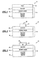
- a composite optical device 10 is fabricated by first depositing a poly-silicon layer 12 on a SOI structure 14. If desired, a thin dielectric may be provided between the poly-silicon layer 12 and SOI structure 14 to help confine dopants and to facilitate poly patterning. This dielectric may be a gate oxide and may have a thickness of 30-100 ⁇ .
- the poly-silicon layer 12 is preferably, although not necessarily, as crystalline as possible to minimize losses and is indexed-matched to the SOI structure 14 to allow uniform expansion of a light beam into the poly-silicon layer 12 from the SOI structure 14.
- the SOI structure 14 includes a silicon handle wafer 16, a buried oxide layer 18 formed over the silicon handle wafer 16, and a silicon layer 20 formed over the buried oxide layer 18.
- the silicon layer 20, for example, may be formed from single crystal silicon.
- the thickness of the poly-silicon layer 12, for example may be on the order of 1200-1600 ⁇ .
- the thickness of the SOI structure 14, for example may be on the order of 1200-1600 ⁇ .
- the poly-silicon layer 12 is patterned to form the appropriate features, such as a poly-silicon rib 22, of a desired optical device.
- the poly-silicon layer 12 is patterned to form, or to contribute to the formation of, a light guiding rib of the optical waveguide.
- the poly-silicon rib 22 may be formed, for example, by placing an appropriate mask over the poly-silicon layer 12, and by applying an etchant to remove the unwanted poly-silicon.
- the poly-silicon layer 12 may be etched selectively with respect to the underlying (oxidized) SOI structure 14.
- a dry etchant such as a plasma, may be used for this purpose to maximize control.
- an oxide layer 24 is formed over the exposed silicon layer 20 and the poly-silicon rib 22.
- the oxide layer 24 may have a thickness, for example, of approximately 30 to 100 ⁇ .
- the oxide layer 24 is used as an etch stop during the subsequent etching described below.
- the oxide layer 24 can also provide gate oxide for other devices formed on the SOI structure 14.
- the oxide layer 24, however, may be omitted if desired.
- Other dielectric materials such as silicon nitride could be used in place of the oxide in the oxide layer 24.
- a conformal amorphous or poly-silicon layer 26 is deposited over the oxide layer 24.
- the thickness of the conformal amorphous or poly-silicon layer 26, for example, may be on the order of 2000 to 3000 ⁇ .
- the conformal amorphous or poly-silicon layer 26 is anisotropically etched until the material is removed from all horizontal surfaces, leaving amorphous or poly-silicon spacers 28 and 30 along the side walls of the original poly-silicon rib 22. These amorphous or poly-silicon spacers 28 and 30 round the corners of the poly-silicon rib 22, thus reducing the optical losses and improving the performance of the optical device 10.
- the process described above does not rely on complex isotropic/anisotropic etching, oxidation, potentially damaging chemical mechanical planarization (CMP), or physical sputtering processes that are available in a typical fabrication facility.
- CMP chemical mechanical planarization
- the process described above instead utilizes simple poly or amorphous silicon deposition and anisotropic etching processes to create a composite silicon structure with the necessary rounded edges.
- spacers and the process of forming these spacers as described herein produces the desired rounded corners and/or reduces or eliminates the problems of the other processes described herein.
- the spacers can be implemented along portions of the SOI or SOI/poly wave guide to reduce edge non-uniformities and round corners to minimize losses. Spacers are also useful for facilitating light transmission from a SOI waveguide to a composite SOI/poly-silicon waveguide.
- the process described herein is very compatible with the formation of integrated opto-electronic devices.
- the poly-silicon layer 12 can be deposited and patterned to form the poly-silicon rib 22 and can also be deposited and patterned over a suitable well region or regions.
- the well region or regions can be suitably implanted, and an oxide layer (such as the oxide layer 24) can be grown to also form a gate oxide.
- the conformal amorphous or poly-silicon layer 26 can be deposited, masked, and etched to form not only the amorphous or poly-silicon spacers 28 and 30, but also one or more gates of electronic devices.
- the process disclosed herein can utilize planar isolation such as shallow trench isolation, the amorphous or poly-silicon spacers 28 and 30 can be left around the poly-silicon rib 22 without compromising the fidelity of the gate pattern.
- the process sequence can then continue along the conventional flow.
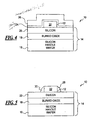
- the opto-electronic device 50 is fabricated by first depositing a poly-silicon layer 52 on a SOI structure 54. If desired, a thin dielectric may be provided between the poly-silicon layer 52 and SOI structure 54 to help confine dopants and to facilitate poly patterning.
- the SOI structure 54 includes a silicon handle wafer 56, a buried oxide layer 58 formed over the silicon handle wafer 56, and a silicon layer 60 formed over the buried oxide layer 58.
- the silicon layer 60 for example, may be formed from single crystal silicon.
- Shallow trenches 62 and 64 are formed in the silicon layer 20 resulting in silicon islands 66, 68, and 70.
- the poly-silicon layer 52 is patterned to form a poly-silicon rib 72 of an optical device 74 and a poly-silicon gate 76 of an electronic device 78.
- the poly-silicon rib 72 is thus formed on the silicon island 68, and the poly-silicon gate 76 is formed on the silicon island 70.
- the poly-silicon rib 72 and the poly-silicon gate 76 may themselves be referred to as silicon islands, albeit poly-silicon islands.
- the electronic device 78 may also include silicide regions 80, 82, and 84 and oxide spacers 86 and 88.
- the optical device 74 includes poly-silicon spacers 90 and 92 as described above. Moreover, because the requirements of the optical device 74 and of the electronic device 78 may differ, it can difficult to create the optical devices and gates of electronic devices in the same poly-silicon layer. If so, a second poly-silicon (spacer) layer can be used to construct the gates.
- the vertical edges of the silicon island 68 of the optical device 74 may also be provided with poly-silicon spacers 94 and 96.
- the silicon island 68 for example, can be used to also guide light.
- the present invention can be used in connection with optical devices other than optical waveguides.
- the present invention can also be used in connection with optical modulators, optical switches, etc.
Landscapes
- Physics & Mathematics (AREA)
- Engineering & Computer Science (AREA)
- Microelectronics & Electronic Packaging (AREA)
- General Physics & Mathematics (AREA)
- Optics & Photonics (AREA)
- Optical Integrated Circuits (AREA)
- Thin Film Transistor (AREA)
- Light Receiving Elements (AREA)
Claims (10)
- Verfahren zum Herstellen eines optischen Bauelements (10), wobei das Verfahren folgendes umfaßt:Ausbilden einer Siliziuminsel des optischen Bauelements derart, daß die Siliziuminsel Seitenwände aufweist, wobei das Ausbilden der Siliziuminsel das Ausbilden einer Siliziumrippe (22) auf einem SOI-Substrat (14) umfaßt, so daß ein Abschnitt des SOI-Substrats (14) exponiert ist und so daß die Siliziumrippe (22) Seitenwände aufweist; undAusbilden von Siliziumabstandshaltern (28, 30) entlang der Seitenwände, um Ecken der Siliziuminsel abzurunden, wobei das Ausbilden der Siliziumabstandshalter folgendes umfaßt:Ausbilden einer Siliziumschicht (24) über der Siliziumrippe (22) und dem exponierten SOI-Substrat (14) undEntfernen der Siliziumschicht (24), um Siliziumabstandshalter (28, 30) entlang der Seitenwände bereitzustellen, um die Ecken der Siliziumrippe (22) abzurunden.
- Verfahren nach Anspruch 1, wobei das Entfernen der Siliziumschicht (24) das anisotrope Ätzen der Siliziumschicht umfaßt, um die Siliziumabstandshalter (28, 30) entlang der Seitenwände zurückzulassen, um die Ecken der Siliziumrippe (22) abzurunden.
- Verfahren nach Anspruch 2, wobei das Ausbilden einer Siliziumrippe (22) auf einem SOI-Substrat (14) folgendes umfaßt:Ausbilden einer Polysiliziumschicht (12) über dem SOI-Substrat (14);Maskieren der Polysiliziumschicht (12) undÄtzen der Polysiliziumschicht (12) zum Ausbilden einer Polysiliziumrippe (22).
- Verfahren nach Anspruch 2, wobei das Ausbilden einer Siliziumschicht (24) über der Siliziumrippe (22) und dem exponierten SOI-Substrat (14) folgendes umfaßt:Ausbilden einer konformen Oxidschicht (24) über der Rippe (22) und dem exponierten SOI-Substrat (14) undAusbilden einer konformen Polysiliziumschicht über der Oxidschicht (24).
- Verfahren nach Anspruch 4, wobei das Ausbilden einer Siliziumrippe (22) auf einem SOI-Substrat (14) folgendes umfaßt:Ausbilden einer Polysiliziumschicht (12) über dem SOI-Substrat (14);Maskieren der Polysiliziumschicht (12) undÄtzen der Polysiliziumschicht (12) zum Ausbilden einer Polysiliziumrippe (22).
- Verfahren nach Anspruch 1, wobei das Ausbilden einer Siliziumrippe (22) auf einem SOI-Substrat (14) das Ausbilden einer Polysiliziumrippe (22) auf einem SOI-Substrat (14) umfaßt, so daß ein Abschnitt des SOI-Substrats (14) exponiert ist und so daß die Polysiliziumrippe (22) Seitenwände aufweist.
- Verfahren nach Anspruch 6, wobei das Entfernen der Siliziumschicht (24) das anisotrope Ätzen der Siliziumschicht (24) umfaßt, um die Siliziumabstandshalter (28, 30) entlang der Seitenwände zurückzulassen, um die Ecken der Siliziumrippe (22) abzurunden.
- Verfahren nach Anspruch 1, wobei das optische Bauelement 10 einen optischen Wellenleiter umfaßt.
- Verfahren nach Anspruch 1, wobei das SOI-Substrat (14) einen Silizium-Handle-Wafer, eine vergrabene Oxidschicht über dem Silizium-Handle-Wafer und eine einkristalline Siliziumschicht über der vergrabenen Oxidschicht umfaßt und wobei das Ausbilden einer Siliziumrippe (22) auf einem SOI-Substrat (14) das Ausbilden einer Polysiliziumrippe auf dem einkristallinen Silizium umfaßt, so daß ein Abschnitt des einkristallinen Siliziums exponiert ist und so daß die Polysiliziumrippe Seitenwände aufweist.
- Verfahren nach Anspruch 9, wobei das Entfernen der Siliziumschicht (24) das anisotrope Ätzen der Siliziumschicht (24) umfaßt, um die Siliziumabstandshalter (28, 30) entlang der Seitenwände zurückzulassen, um die Ecken der Siliziumrippe (22) abzurunden.
Applications Claiming Priority (2)
| Application Number | Priority Date | Filing Date | Title |
|---|---|---|---|
| US10/755,212 US7672558B2 (en) | 2004-01-12 | 2004-01-12 | Silicon optical device |
| PCT/US2005/001117 WO2005071455A2 (en) | 2004-01-12 | 2005-01-11 | Silicon optical device |
Publications (2)
| Publication Number | Publication Date |
|---|---|
| EP1704433A2 EP1704433A2 (de) | 2006-09-27 |
| EP1704433B1 true EP1704433B1 (de) | 2009-03-18 |
Family
ID=34739536
Family Applications (1)
| Application Number | Title | Priority Date | Filing Date |
|---|---|---|---|
| EP05711427A Expired - Fee Related EP1704433B1 (de) | 2004-01-12 | 2005-01-11 | Optisches siliziumbauelement |
Country Status (6)
| Country | Link |
|---|---|
| US (1) | US7672558B2 (de) |
| EP (1) | EP1704433B1 (de) |
| JP (1) | JP2007519041A (de) |
| DE (1) | DE602005013349D1 (de) |
| TW (1) | TW200537144A (de) |
| WO (1) | WO2005071455A2 (de) |
Families Citing this family (25)
| Publication number | Priority date | Publication date | Assignee | Title |
|---|---|---|---|---|
| US7118682B2 (en) * | 2003-03-28 | 2006-10-10 | Sioptical, Inc. | Low loss SOI/CMOS compatible silicon waveguide and method of making the same |
| US7672558B2 (en) | 2004-01-12 | 2010-03-02 | Honeywell International, Inc. | Silicon optical device |
| US7016587B2 (en) * | 2004-01-20 | 2006-03-21 | Xerox Corporation | Low loss silicon waveguide and method of fabrication thereof |
| US7217584B2 (en) * | 2004-03-18 | 2007-05-15 | Honeywell International Inc. | Bonded thin-film structures for optical modulators and methods of manufacture |
| US7177489B2 (en) * | 2004-03-18 | 2007-02-13 | Honeywell International, Inc. | Silicon-insulator-silicon thin-film structures for optical modulators and methods of manufacture |
| US20050214989A1 (en) * | 2004-03-29 | 2005-09-29 | Honeywell International Inc. | Silicon optoelectronic device |
| US7550382B2 (en) * | 2005-05-31 | 2009-06-23 | Semiconductor Energy Laboratory Co., Ltd. | Manufacturing method of semiconductor device, evaluation method of semiconductor device, and semiconductor device |
| US20070101927A1 (en) * | 2005-11-10 | 2007-05-10 | Honeywell International Inc. | Silicon based optical waveguide structures and methods of manufacture |
| US7362443B2 (en) * | 2005-11-17 | 2008-04-22 | Honeywell International Inc. | Optical gyro with free space resonator and method for sensing inertial rotation rate |
| US7514285B2 (en) * | 2006-01-17 | 2009-04-07 | Honeywell International Inc. | Isolation scheme for reducing film stress in a MEMS device |
| US20070274655A1 (en) * | 2006-04-26 | 2007-11-29 | Honeywell International Inc. | Low-loss optical device structure |
| US7454102B2 (en) * | 2006-04-26 | 2008-11-18 | Honeywell International Inc. | Optical coupling structure |
| US20080101744A1 (en) * | 2006-10-31 | 2008-05-01 | Honeywell International Inc. | Optical Waveguide Sensor Devices and Methods For Making and Using Them |
| US8290325B2 (en) * | 2008-06-30 | 2012-10-16 | Intel Corporation | Waveguide photodetector device and manufacturing method thereof |
| US8258476B1 (en) * | 2008-07-29 | 2012-09-04 | University Of Washington | Radiation detection using a nonlinear phase shift mechanism |
| US8000565B2 (en) * | 2008-12-31 | 2011-08-16 | Intel Corporation | Buried dual taper waveguide for passive alignment and photonic integration |
| EP2549311B1 (de) | 2011-07-19 | 2014-09-03 | Huawei Technologies Co., Ltd. | Tiefe/flache optische Strahlungsfilter |
| WO2014055562A1 (en) * | 2012-10-01 | 2014-04-10 | Justin Payne | Method of monolithically integrated optoelectrics |
| SG11201510033RA (en) | 2013-06-12 | 2016-01-28 | Massachusetts Inst Technology | Optical modulator from standard fabrication processing |
| US10191213B2 (en) | 2014-01-09 | 2019-01-29 | Globalfoundries Inc. | Shielding structures between optical waveguides |
| WO2017058319A2 (en) | 2015-06-30 | 2017-04-06 | Massachusetts Institute Of Technology | Waveguide-coupled silicon-germanium photodetectors and fabrication methods for same |
| US11105974B2 (en) | 2015-06-30 | 2021-08-31 | Massachusetts Institute Of Technology | Waveguide-coupled silicon-germanium photodetectors and fabrication methods for same |
| US10620371B2 (en) * | 2016-03-05 | 2020-04-14 | Huawei Technologies Canada Co., Ltd. | Waveguide crossing having rib waveguides |
| US9798166B1 (en) * | 2017-01-24 | 2017-10-24 | Mellanox Technologies Silicon Photonics Inc. | Attenuator with improved fabrication consistency |
| US11860417B2 (en) * | 2019-09-09 | 2024-01-02 | Cisco Technology, Inc. | Precision spacing control for optical waveguides |
Family Cites Families (119)
| Publication number | Priority date | Publication date | Assignee | Title |
|---|---|---|---|---|
| US4234357A (en) * | 1979-07-16 | 1980-11-18 | Trw Inc. | Process for manufacturing emitters by diffusion from polysilicon |
| US4315693A (en) | 1979-12-31 | 1982-02-16 | Walker Clifford G | Optical strapdown inertia system |
| US4673293A (en) | 1985-01-31 | 1987-06-16 | Honeywell Inc. | Passive cavity gyro bias eliminator |
| US5163118A (en) | 1986-11-10 | 1992-11-10 | The United States Of America As Represented By The Secretary Of The Air Force | Lattice mismatched hetrostructure optical waveguide |
| US4886345A (en) | 1988-08-05 | 1989-12-12 | Harris Corporation | Electro-optical phase modulator |
| GB2221999B (en) | 1988-08-16 | 1992-09-16 | Plessey Co Plc | Optical phase modulator |
| US4958898A (en) | 1989-03-15 | 1990-09-25 | The United States Of America As Represented By The Secretary Of The Air Force | Silicon double-injection electro-optic modulator with insulated-gate and method of using same |
| EP0393987A3 (de) | 1989-04-19 | 1992-08-05 | British Aerospace Public Limited Company | Optischer Ringresonatorkreisel |
| US5143577A (en) * | 1991-02-08 | 1992-09-01 | Hoechst Celanese Corporation | Smooth-wall polymeric channel and rib waveguides exhibiting low optical loss |
| KR0134763B1 (ko) | 1992-04-21 | 1998-04-23 | 다니이 아끼오 | 광도파로소자와 그 제조방법 |
| US5383048A (en) | 1993-02-03 | 1995-01-17 | Seaver; George | Stress-optical phase modulator and modulation system and method of use |
| KR960011653B1 (ko) | 1993-04-16 | 1996-08-24 | 현대전자산업 주식회사 | 디램 셀 및 그 제조방법 |
| CA2172278C (en) | 1993-09-21 | 2003-04-08 | Stephen James Crampton | An electro-optic device |
| US5429981A (en) | 1994-06-30 | 1995-07-04 | Honeywell Inc. | Method of making linear capacitors for high temperature applications |
| US5696662A (en) | 1995-08-21 | 1997-12-09 | Honeywell Inc. | Electrostatically operated micromechanical capacitor |
| JP2817703B2 (ja) | 1996-04-25 | 1998-10-30 | 日本電気株式会社 | 光半導体装置 |
| US5841931A (en) | 1996-11-26 | 1998-11-24 | Massachusetts Institute Of Technology | Methods of forming polycrystalline semiconductor waveguides for optoelectronic integrated circuits, and devices formed thereby |
| US5861651A (en) | 1997-02-28 | 1999-01-19 | Lucent Technologies Inc. | Field effect devices and capacitors with improved thin film dielectrics and method for making same |
| US6147362A (en) | 1997-03-17 | 2000-11-14 | Honeywell International Inc. | High performance display pixel for electronics displays |
| US5917967A (en) | 1997-05-21 | 1999-06-29 | The United States Of America As Represented By The Secretary Of The Army | Techniques for forming optical electronic integrated circuits having interconnects in the form of semiconductor waveguides |
| SG70141A1 (en) | 1997-12-26 | 2000-01-25 | Canon Kk | Sample separating apparatus and method and substrate manufacturing method |
| US6108212A (en) | 1998-06-05 | 2000-08-22 | Motorola, Inc. | Surface-mount device package having an integral passive component |
| US6381380B1 (en) | 1998-06-24 | 2002-04-30 | The Trustees Of Princeton University | Twin waveguide based design for photonic integrated circuits |
| US6270604B1 (en) | 1998-07-23 | 2001-08-07 | Molecular Optoelectronics Corporation | Method for fabricating an optical waveguide |
| JP2000124092A (ja) | 1998-10-16 | 2000-04-28 | Shin Etsu Handotai Co Ltd | 水素イオン注入剥離法によってsoiウエーハを製造する方法およびこの方法で製造されたsoiウエーハ |
| US6493089B2 (en) | 1998-10-19 | 2002-12-10 | Canon Kabushiki Kaisha | Gyro and method of operating the same with a modulated frequency signal |
| GB2343293B (en) | 1998-10-23 | 2003-05-14 | Bookham Technology Ltd | Manufacture of a silicon waveguide structure |
| JP4416055B2 (ja) | 1998-12-01 | 2010-02-17 | ローム株式会社 | 強誘電体メモリおよびその製造方法 |
| US6323985B1 (en) | 1998-12-30 | 2001-11-27 | Intel Corporation | Mosfet through silicon modulator and method |
| US6150266A (en) | 1999-01-28 | 2000-11-21 | Vlsi Technology, Inc. | Local interconnect formed using silicon spacer |
| US6627954B1 (en) | 1999-03-19 | 2003-09-30 | Silicon Wave, Inc. | Integrated circuit capacitor in a silicon-on-insulator integrated circuit |
| JP2001111160A (ja) | 1999-04-19 | 2001-04-20 | Canon Inc | 半導体素子の製造方法及び半導体素子、リング共振器型半導体レーザ、ジャイロ |
| US6555288B1 (en) * | 1999-06-21 | 2003-04-29 | Corning Incorporated | Optical devices made from radiation curable fluorinated compositions |
| JP2001042150A (ja) | 1999-07-30 | 2001-02-16 | Canon Inc | 光導波路、その作製方法、およびこれを用いた光インタコネクション装置 |
| GB2355312B (en) | 1999-10-13 | 2001-09-12 | Bookham Technology Ltd | Method of fabricating an integrated optical component |
| SE0000148D0 (sv) * | 2000-01-17 | 2000-01-17 | Forskarpatent I Syd Ab | Tillverkningsförfarande för IR-detektormatriser |
| US6546538B1 (en) | 2000-03-10 | 2003-04-08 | Lsi Logic Corporation | Integrated circuit having on-chip capacitors for supplying power to portions of the circuit requiring high-transient peak power |
| FR2810991B1 (fr) | 2000-06-28 | 2004-07-09 | Inst Francais Du Petrole | Procede pour l'hydrogenation de coupes contenant des hydrocarbures et notamment des molecules insaturees contenant au moins deux doubles liaisons ou au moins une triple liaison |
| JP4961634B2 (ja) | 2000-07-07 | 2012-06-27 | Kddi株式会社 | 光ゲート装置 |
| US6850683B2 (en) * | 2000-07-10 | 2005-02-01 | Massachusetts Institute Of Technology | Low-loss waveguide and method of making same |
| US6674108B2 (en) | 2000-12-20 | 2004-01-06 | Honeywell International Inc. | Gate length control for semiconductor chip design |
| FR2819893B1 (fr) * | 2001-01-25 | 2003-10-17 | Opsitech Optical System Chip | Structure optique integree a birefringence reduite |
| US6890450B2 (en) | 2001-02-02 | 2005-05-10 | Intel Corporation | Method of providing optical quality silicon surface |
| WO2002069004A2 (en) | 2001-02-22 | 2002-09-06 | Bookham Technology Plc | Semiconductor optical waveguide device |
| US6603166B2 (en) | 2001-03-14 | 2003-08-05 | Honeywell International Inc. | Frontside contact on silicon-on-insulator substrate |
| US6633716B2 (en) * | 2001-05-02 | 2003-10-14 | Motorola, Inc. | Optical device and method therefor |
| US6842546B2 (en) | 2001-05-17 | 2005-01-11 | Sioptical, Inc. | Polyloaded optical waveguide device in combination with optical coupler, and method for making same |
| US6608945B2 (en) | 2001-05-17 | 2003-08-19 | Optronx, Inc. | Self-aligning modulator method and associated apparatus |
| US6748125B2 (en) | 2001-05-17 | 2004-06-08 | Sioptical, Inc. | Electronic semiconductor control of light in optical waveguide |
| US6690844B2 (en) | 2001-05-17 | 2004-02-10 | Optronx, Inc. | Optical fiber apparatus and associated method |
| US6898352B2 (en) | 2001-05-17 | 2005-05-24 | Sioptical, Inc. | Optical waveguide circuit including passive optical waveguide device combined with active optical waveguide device, and method for making same |
| US6963118B2 (en) | 2001-05-17 | 2005-11-08 | Sioptical, Inc. | Hybrid active and electronic circuit with evanescent coupling |
| US6654511B2 (en) | 2001-05-17 | 2003-11-25 | Sioptical, Inc. | Optical modulator apparatus and associated method |
| US6526187B1 (en) | 2001-05-17 | 2003-02-25 | Optronx, Inc. | Polarization control apparatus and associated method |
| US6690863B2 (en) | 2001-05-17 | 2004-02-10 | Si Optical, Inc. | Waveguide coupler and method for making same |
| US6603889B2 (en) | 2001-05-17 | 2003-08-05 | Optronx, Inc. | Optical deflector apparatus and associated method |
| US6646747B2 (en) | 2001-05-17 | 2003-11-11 | Sioptical, Inc. | Interferometer apparatus and associated method |
| US6760498B2 (en) | 2001-05-17 | 2004-07-06 | Sioptical, Inc. | Arrayed waveguide grating, and method of making same |
| US6625348B2 (en) | 2001-05-17 | 2003-09-23 | Optron X, Inc. | Programmable delay generator apparatus and associated method |
| US6891985B2 (en) | 2001-05-17 | 2005-05-10 | Sioptical, Inc. | Polyloaded optical waveguide devices and methods for making same |
| US6891685B2 (en) | 2001-05-17 | 2005-05-10 | Sioptical, Inc. | Anisotropic etching of optical components |
| US6658173B2 (en) | 2001-05-17 | 2003-12-02 | Optronx, Inc. | Interferometer and method of making same |
| US6738546B2 (en) | 2001-05-17 | 2004-05-18 | Sioptical, Inc. | Optical waveguide circuit including multiple passive optical waveguide devices, and method of making same |
| US6912330B2 (en) | 2001-05-17 | 2005-06-28 | Sioptical Inc. | Integrated optical/electronic circuits and associated methods of simultaneous generation thereof |
| US6947615B2 (en) | 2001-05-17 | 2005-09-20 | Sioptical, Inc. | Optical lens apparatus and associated method |
| US6493502B1 (en) | 2001-05-17 | 2002-12-10 | Optronx, Inc. | Dynamic gain equalizer method and associated apparatus |
| US6596570B2 (en) | 2001-06-06 | 2003-07-22 | International Business Machines Corporation | SOI device with reduced junction capacitance |
| US20030026571A1 (en) * | 2001-07-31 | 2003-02-06 | Michael Bazylenko | Method of reducing sidewall roughness of a waveguide |
| US6990257B2 (en) * | 2001-09-10 | 2006-01-24 | California Institute Of Technology | Electronically biased strip loaded waveguide |
| US6816636B2 (en) | 2001-09-12 | 2004-11-09 | Honeywell International Inc. | Tunable optical filter |
| JP3755588B2 (ja) | 2001-10-03 | 2006-03-15 | 日本電気株式会社 | 光制御デバイス |
| US6580863B2 (en) | 2001-10-31 | 2003-06-17 | Intel Corporation | System and method for providing integrated optical waveguide device |
| US20030098289A1 (en) | 2001-11-29 | 2003-05-29 | Dawei Zheng | Forming an optical mode transformer |
| WO2003065413A2 (en) | 2002-01-30 | 2003-08-07 | Optronx, Inc. | Method and apparatus for altering the effective mode index of waveguide |
| JP3955764B2 (ja) | 2002-02-08 | 2007-08-08 | 富士通株式会社 | 電気光学効果により光位相を変化させる素子を搭載した光変調器 |
| JP2003234410A (ja) | 2002-02-08 | 2003-08-22 | Fujitsu Ltd | キャパシタ及びその製造方法並びに半導体装置 |
| IL148716A0 (en) | 2002-03-14 | 2002-09-12 | Yissum Res Dev Co | Control of optical signals by mos (cosmos) device |
| US6956983B2 (en) | 2002-05-31 | 2005-10-18 | Intel Corporation | Epitaxial growth for waveguide tapering |
| US7010208B1 (en) * | 2002-06-24 | 2006-03-07 | Luxtera, Inc. | CMOS process silicon waveguides |
| US6743662B2 (en) | 2002-07-01 | 2004-06-01 | Honeywell International, Inc. | Silicon-on-insulator wafer for RF integrated circuit |
| US6919238B2 (en) | 2002-07-29 | 2005-07-19 | Intel Corporation | Silicon on insulator (SOI) transistor and methods of fabrication |
| US6888219B2 (en) | 2002-08-29 | 2005-05-03 | Honeywell International, Inc. | Integrated structure with microwave components |
| US7020374B2 (en) | 2003-02-03 | 2006-03-28 | Freescale Semiconductor, Inc. | Optical waveguide structure and method for fabricating the same |
| US6845198B2 (en) | 2003-03-25 | 2005-01-18 | Sioptical, Inc. | High-speed silicon-based electro-optic modulator |
| US6993225B2 (en) | 2004-02-10 | 2006-01-31 | Sioptical, Inc. | Tapered structure for providing coupling between external optical device and planar optical waveguide and method of forming the same |
| US7118682B2 (en) | 2003-03-28 | 2006-10-10 | Sioptical, Inc. | Low loss SOI/CMOS compatible silicon waveguide and method of making the same |
| US6897498B2 (en) | 2003-03-31 | 2005-05-24 | Sioptical, Inc. | Polycrystalline germanium-based waveguide detector integrated on a thin silicon-on-insulator (SOI) platform |
| US7020364B2 (en) | 2003-03-31 | 2006-03-28 | Sioptical Inc. | Permanent light coupling arrangement and method for use with thin silicon optical waveguides |
| US7000207B2 (en) | 2003-04-10 | 2006-02-14 | Sioptical, Inc. | Method of using a Manhattan layout to realize non-Manhattan shaped optical structures |
| US6934444B2 (en) | 2003-04-10 | 2005-08-23 | Sioptical, Inc. | Beam shaping and practical methods of reducing loss associated with mating external sources and optics to thin silicon waveguides |
| US6980720B2 (en) | 2003-04-11 | 2005-12-27 | Sioptical, Inc. | Mode transformation and loss reduction in silicon waveguide structures utilizing tapered transition regions |
| CA2520972C (en) | 2003-04-21 | 2010-01-26 | Sioptical, Inc. | Cmos-compatible integration of silicon-based optical devices with electronic devices |
| EP1625424A4 (de) | 2003-04-23 | 2009-04-15 | Siophcal Inc | Auf einer optischen soi-plattform gebildete planare submikrometer-lichtwelleneinrichtungen |
| JP2006526808A (ja) | 2003-04-28 | 2006-11-24 | シオプティカル インコーポレーテッド | プリズム結合したsoiベースの光学系で波長感受性を下げるための構成 |
| KR100794817B1 (ko) | 2003-05-08 | 2008-01-15 | 시옵티컬 인코포레이티드 | 고속 실리콘-기반 전기-광학 변조기 |
| WO2005024469A2 (en) | 2003-09-04 | 2005-03-17 | Sioptical, Inc. | Interfacing multiple wavelength sources to thin optical waveguides utilizing evanescent coupling |
| US7003196B2 (en) | 2003-09-04 | 2006-02-21 | Sioptical, Inc. | External grating structures for interfacing wavelength-division-multiplexed optical sources with thin optical waveguides |
| CN100440522C (zh) | 2003-11-20 | 2008-12-03 | 斯欧普迪克尔股份有限公司 | 硅基肖特基势垒红外光检测器 |
| US7113676B2 (en) | 2003-12-04 | 2006-09-26 | David Piede | Planar waveguide optical isolator in thin silicon-on-isolator (SOI) structure |
| US20050135727A1 (en) | 2003-12-18 | 2005-06-23 | Sioptical, Inc. | EMI-EMC shield for silicon-based optical transceiver |
| US7672558B2 (en) | 2004-01-12 | 2010-03-02 | Honeywell International, Inc. | Silicon optical device |
| US7013067B2 (en) | 2004-02-11 | 2006-03-14 | Sioptical, Inc. | Silicon nanotaper couplers and mode-matching devices |
| US7298949B2 (en) | 2004-02-12 | 2007-11-20 | Sioptical, Inc. | SOI-based photonic bandgap devices |
| EP1743376B1 (de) | 2004-02-26 | 2015-09-02 | Cisco Technology, Inc. | Aktive lichtmanipulation in einer soi-struktur (soi - silicon-on-insulator) |
| US7109739B2 (en) | 2004-03-08 | 2006-09-19 | Sioptical, Inc. | Wafer-level opto-electronic testing apparatus and method |
| US7217584B2 (en) | 2004-03-18 | 2007-05-15 | Honeywell International Inc. | Bonded thin-film structures for optical modulators and methods of manufacture |
| US7149388B2 (en) | 2004-03-18 | 2006-12-12 | Honeywell International, Inc. | Low loss contact structures for silicon based optical modulators and methods of manufacture |
| US7177489B2 (en) | 2004-03-18 | 2007-02-13 | Honeywell International, Inc. | Silicon-insulator-silicon thin-film structures for optical modulators and methods of manufacture |
| JP2008504562A (ja) | 2004-03-24 | 2008-02-14 | シオプティカル インコーポレーテッド | 薄いシリコン中の光クロスオーバ |
| US20050214989A1 (en) | 2004-03-29 | 2005-09-29 | Honeywell International Inc. | Silicon optoelectronic device |
| US20050236619A1 (en) | 2004-04-21 | 2005-10-27 | Vipulkumar Patel | CMOS-compatible integration of silicon-based optical devices with electronic devices |
| CA2581451C (en) | 2004-06-23 | 2013-09-24 | Sioptical, Inc. | Integrated approach for design, simulation and verification of monolithic, silicon-based opto-electronic circuits |
| US20060018597A1 (en) | 2004-07-23 | 2006-01-26 | Sioptical, Inc. | Liquid crystal grating coupling |
| US20060038144A1 (en) | 2004-08-23 | 2006-02-23 | Maddison John R | Method and apparatus for providing optimal images of a microscope specimen |
| US20060063679A1 (en) | 2004-09-17 | 2006-03-23 | Honeywell International Inc. | Semiconductor-insulator-semiconductor structure for high speed applications |
| CN101283300B (zh) | 2004-10-19 | 2010-09-22 | 斯欧普迪克尔股份有限公司 | 光学检测器结构以及在单片集成光电装置中作为反馈控制的应用 |
| US20070101927A1 (en) | 2005-11-10 | 2007-05-10 | Honeywell International Inc. | Silicon based optical waveguide structures and methods of manufacture |
| US7362443B2 (en) | 2005-11-17 | 2008-04-22 | Honeywell International Inc. | Optical gyro with free space resonator and method for sensing inertial rotation rate |
| US7372574B2 (en) | 2005-12-09 | 2008-05-13 | Honeywell International Inc. | System and method for stabilizing light sources in resonator gyro |
-
2004
- 2004-01-12 US US10/755,212 patent/US7672558B2/en not_active Expired - Fee Related
-
2005
- 2005-01-11 JP JP2006549600A patent/JP2007519041A/ja not_active Withdrawn
- 2005-01-11 WO PCT/US2005/001117 patent/WO2005071455A2/en active Application Filing
- 2005-01-11 DE DE602005013349T patent/DE602005013349D1/de not_active Expired - Fee Related
- 2005-01-11 EP EP05711427A patent/EP1704433B1/de not_active Expired - Fee Related
- 2005-01-12 TW TW094100890A patent/TW200537144A/zh unknown
Also Published As
| Publication number | Publication date |
|---|---|
| EP1704433A2 (de) | 2006-09-27 |
| JP2007519041A (ja) | 2007-07-12 |
| WO2005071455A2 (en) | 2005-08-04 |
| WO2005071455A3 (en) | 2005-10-06 |
| DE602005013349D1 (de) | 2009-04-30 |
| US20050152658A1 (en) | 2005-07-14 |
| US7672558B2 (en) | 2010-03-02 |
| TW200537144A (en) | 2005-11-16 |
Similar Documents
| Publication | Publication Date | Title |
|---|---|---|
| EP1704433B1 (de) | Optisches siliziumbauelement | |
| EP1754088A1 (de) | Optoelektronisches siliziumbauelement | |
| EP0375632B1 (de) | Verfahren zur Herstellung von Gräben mit abgerundeter Unterseite in einem Siliziumsubstrat zur Herstellung von Isolationen für Grabenstrukturen | |
| EP1026728A2 (de) | Substrat und zugehöriges Herstellungsverfahren | |
| EP0424905B1 (de) | Verfahren zur Herstellung einer Halbleiteranordnung | |
| US7338848B1 (en) | Method for opto-electronic integration on a SOI substrate and related structure | |
| US7067387B2 (en) | Method of manufacturing dielectric isolated silicon structure | |
| JP2006120715A (ja) | 半導体ウェハの製造方法 | |
| JP2001351865A (ja) | 半導体装置の製造方法 | |
| JP3572713B2 (ja) | 半導体量子細線デバイスの製造方法 | |
| JP2008124399A (ja) | 半導体装置の製造方法 | |
| KR100515383B1 (ko) | 서로 다른 두께의 게이트 산화막을 포함하는 트랜지스터형성 방법 | |
| JPH0422021B2 (de) | ||
| CN109148354B (zh) | 半导体结构及其形成方法 | |
| KR100417195B1 (ko) | 반도체 소자의 제조방법 | |
| KR100762865B1 (ko) | 플래쉬 메모리 소자의 제조방법 | |
| JP2786259B2 (ja) | 半導体素子の製造方法 | |
| KR20120062991A (ko) | 에스오아이 기판 및 그 제조방법 | |
| EP0233248A1 (de) | Dielektrische isolationsstruktur für integrierte schaltungen | |
| KR100290901B1 (ko) | 반도체소자의격리막형성방법 | |
| KR100358046B1 (ko) | 플래시 메모리 소자의 제조방법 | |
| KR100416813B1 (ko) | 반도체소자의필드산화막형성방법 | |
| KR100481557B1 (ko) | 더블 질화막 식각을 이용한 내로우 에스티아이 형성방법 | |
| KR100417574B1 (ko) | 반도체소자제조방법 | |
| CN117790298A (zh) | 半导体器件的沟槽制备方法及半导体器件 |
Legal Events
| Date | Code | Title | Description |
|---|---|---|---|
| PUAI | Public reference made under article 153(3) epc to a published international application that has entered the european phase |
Free format text: ORIGINAL CODE: 0009012 |
|
| 17P | Request for examination filed |
Effective date: 20060707 |
|
| AK | Designated contracting states |
Kind code of ref document: A2 Designated state(s): DE FR GB |
|
| 17Q | First examination report despatched |
Effective date: 20061108 |
|
| DAX | Request for extension of the european patent (deleted) | ||
| RBV | Designated contracting states (corrected) |
Designated state(s): DE FR GB |
|
| GRAP | Despatch of communication of intention to grant a patent |
Free format text: ORIGINAL CODE: EPIDOSNIGR1 |
|
| GRAS | Grant fee paid |
Free format text: ORIGINAL CODE: EPIDOSNIGR3 |
|
| GRAA | (expected) grant |
Free format text: ORIGINAL CODE: 0009210 |
|
| AK | Designated contracting states |
Kind code of ref document: B1 Designated state(s): DE FR GB |
|
| REG | Reference to a national code |
Ref country code: GB Ref legal event code: FG4D |
|
| REF | Corresponds to: |
Ref document number: 602005013349 Country of ref document: DE Date of ref document: 20090430 Kind code of ref document: P |
|
| PLBE | No opposition filed within time limit |
Free format text: ORIGINAL CODE: 0009261 |
|
| STAA | Information on the status of an ep patent application or granted ep patent |
Free format text: STATUS: NO OPPOSITION FILED WITHIN TIME LIMIT |
|
| 26N | No opposition filed |
Effective date: 20091221 |
|
| GBPC | Gb: european patent ceased through non-payment of renewal fee |
Effective date: 20100111 |
|
| REG | Reference to a national code |
Ref country code: FR Ref legal event code: ST Effective date: 20100930 |
|
| PG25 | Lapsed in a contracting state [announced via postgrant information from national office to epo] |
Ref country code: FR Free format text: LAPSE BECAUSE OF NON-PAYMENT OF DUE FEES Effective date: 20100201 |
|
| PG25 | Lapsed in a contracting state [announced via postgrant information from national office to epo] |
Ref country code: DE Free format text: LAPSE BECAUSE OF NON-PAYMENT OF DUE FEES Effective date: 20100803 |
|
| PG25 | Lapsed in a contracting state [announced via postgrant information from national office to epo] |
Ref country code: GB Free format text: LAPSE BECAUSE OF NON-PAYMENT OF DUE FEES Effective date: 20100111 |
|
| P01 | Opt-out of the competence of the unified patent court (upc) registered |
Effective date: 20230525 |