US6150266A - Local interconnect formed using silicon spacer - Google Patents
Local interconnect formed using silicon spacer Download PDFInfo
- Publication number
- US6150266A US6150266A US09/239,458 US23945899A US6150266A US 6150266 A US6150266 A US 6150266A US 23945899 A US23945899 A US 23945899A US 6150266 A US6150266 A US 6150266A
- Authority
- US
- United States
- Prior art keywords
- silicon
- layer
- gate
- forming
- local interconnect
- Prior art date
- Legal status (The legal status is an assumption and is not a legal conclusion. Google has not performed a legal analysis and makes no representation as to the accuracy of the status listed.)
- Expired - Lifetime
Links
Images


Classifications
-
- H—ELECTRICITY
- H01—ELECTRIC ELEMENTS
- H01L—SEMICONDUCTOR DEVICES NOT COVERED BY CLASS H10
- H01L21/00—Processes or apparatus adapted for the manufacture or treatment of semiconductor or solid state devices or of parts thereof
- H01L21/70—Manufacture or treatment of devices consisting of a plurality of solid state components formed in or on a common substrate or of parts thereof; Manufacture of integrated circuit devices or of parts thereof
- H01L21/71—Manufacture of specific parts of devices defined in group H01L21/70
- H01L21/768—Applying interconnections to be used for carrying current between separate components within a device comprising conductors and dielectrics
- H01L21/76838—Applying interconnections to be used for carrying current between separate components within a device comprising conductors and dielectrics characterised by the formation and the after-treatment of the conductors
- H01L21/76895—Local interconnects; Local pads, as exemplified by patent document EP0896365
Definitions
- the present claimed invention relates to the field of semiconductor devices. More specifically, the present claimed invention relates to a local interconnect for a semiconductor device.
- SRAM Static Random Access Memory
- dielectric spacers are formed on each side of each gate. A portion of an dielectric spacer is removed using mask and etch steps so as to form a exposed region on the side of the gate.
- SALICIDE Self-aligned silicidation
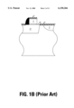
- FIG. 1A shows a diagram of a local interconnect formed according to a prior art process.
- Silicide region 3 extends over the top of polysilicon gate 2 and silicide region 4 extends over silicon substrate 1 such that it at least partially overlies diffusion region 5.
- the sidewall of the polysilicon gate 2 does not form a continuous layer of silicide.
- the poor sidewall silicidation is primarily due to metal thinning associated with sputtering shadowing and to residual surface oxide left over from prior processing steps (polysilicon reoxidation, spacer removal, etc.).
- the gate-to-diffusion connection relies on the silicide at the bottom corner 10 where the sidewall of polysilicon gate 2 meets silicide region 4.
- the resulting electrical connection is unreliable as it relies on electrical connection via the tip of silicide region 4 at bottom corner 10 and relies on conductivity through polysilicon gate 2.
- FIG. 1B shows a disconnection 20 that results from the placement of polysilicon gate 2 over STI dielectric 21. Disconnection problems of this type typically result from photolithography misalignment.
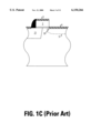
- junction leakage typically occurs as a result of rough silicide formation because the diffusion junction is abruptly delineated along the gate edge, creating a junction punch-through (a conductive path into the semiconductor substrate). This is in contrast to the normal situation where the source/drain extension along a spacer edge provides extra protection against silicidation induced junction leakage.
- FIG. 1C shows junction punch-through 30 that is a conductive path resulting from rough silicide formation during the formation of silicide region 4.
- the present invention provides a local interconnect structure that includes a silicon spacer.
- the local interconnect of the present invention is more robust than prior art interconnect structures.
- gates and spacers are formed on a silicon substrate using conventional fabrication processes.
- polysilicon is deposited, masked and etched to form gates.
- Spacers are then formed by the deposition of a dielectric layer that is etched to form spacers on opposite sides of each gate.
- a portion of a spacer is removed so as to form an open region (exposing a portion of the sidewall of the spacer) where local interconnection is to be formed.
- a thin screen oxide is deposited over the wafer, followed by formation of a diffusion region.
- implantation and rapid-thermal annealing are used to form a diffusion region that includes source/drain structures.
- a layer of silicon (either amorphous or polycrystalline) is then deposited, followed by selective silicon etching to form a silicon spacer along the open region.
- SALICIDE self-aligned silicidation
- the local interconnects of the present invention are more robust and reliable than prior art local interconnects. This is primarily due to the fact that the metal thickness, hence silicide thickness, along the silicon spacer is close to that on the gate and on the diffusion region. More particularly, because the silicide surface in the present invention is raised above the original silicon surface, the outward expansion of silicide will result in a continuous silicide layer formation at the local interconnect. Second, since the metal thickness around the intersection between the silicon spacer and the diffusion region is significantly thicker (approximately 300 Angstroms) than the oxide, there is plenty of metal supply for silicide formation, thus enhancing the formation of a continuous silicide at those interface points. This results in silicide that is reliable at the joint points between the silicon spacer and the diffusion region and between the silicon spacer and the gate.
- STI Shallow Trench Isolation
- Silicidation on the silicon substrate occurs over source/drain regions where the junction is relatively deep. Therefore, rough silicide formation does not result in junction punch-through as occurs in prior art processes. Thus, the local interconnect structure and method of the present invention does not produce junction leakage as occurs in prior art methods.
- the present invention provides a local interconnect structure and a method for forming a local interconnect structure that produces a local interconnect that is robust and that makes good electrical connection. Also the local interconnect structure and the method for making a local interconnect structure of the present invention does not have silicidation induced junction leakage.
- FIG. 1A is a cross-sectional view illustrating a prior art process for forming a local interconnect.
- FIG. 1B is a cross-sectional view illustrating a prior art interconnect having a disconnect.
- FIG. 1C is a cross-sectional view illustrating a prior art local interconnect having junction punch-through.
- FIG. 2 is a flow chart showing steps for forming a local interconnect in accordance with the present claimed invention.
- FIG. 3 is a cross-sectional view illustrating a semiconductor substrate having gates and spacers formed thereon in accordance with the present claimed invention.
- FIG. 4 is a cross-sectional view illustrating the structure of FIG. 3 after the removal of a portion of a spacer in accordance with the present claimed invention.
- FIG. 5 is a cross-sectional view illustrating the deposition of an oxide layer over the structure shown in FIG. 4 in accordance with the present claimed invention.
- FIG. 6 is a cross-sectional view illustrating the formation of a diffusion region in accordance with the present claimed invention.
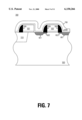
- FIG. 7 is a cross-sectional view illustrating the deposition of a layer of silicon in accordance with the present claimed invention.
- FIG. 8 is a cross-sectional view illustrating the formation of a silicon spacer in accordance with the present claimed invention.
- FIG. 9 is a cross-sectional view illustrating the formation of a silicide region in accordance with the present claimed invention.
- a gate and spacers are formed on a semiconductor substrate as shown by step 101.
- a polysilicon gate is formed having spacers on both sides thereof.
- structure 300 includes gate 301 and gate 302 that are formed on substrate 303.
- gates 301-302 are formed of polysilicon and have a thickness in the range of 1500-3000 Angstroms.
- Spacers 306-307 extend on opposite sides of gate 301 and spacers 308-309 extend on opposite sides of gate 302.
- spacers 306-309 are formed of Tetra Ethyl Ortho Silicate (TEOS) based silicon oxide.
- structure 300 includes shallow trench isolation (STI) that isolates active areas using shallow trenches that are filled with dielectric such as trench 310.
- STI shallow trench isolation
- a portion of a spacer is removed so as to form an open region where the local interconnection is to be formed.
- spacer removal is performed using a conventional photolithography process followed by an oxide etch step. That is, conventional photolithography techniques are used to selectively mask the structure 30b. An etch step is then performed so as to remove the desired portion of the spacer.
- FIG. 4 structure 300 is shown after a portion of spacer 307 (shown in FIG. 3) has been removed, leaving an open region 390 of gate 301 that exposes a portion of sidewall 391 of spacer 307.
- an oxide layer is deposited.
- the oxide layer is a thin layer of TEOS-based oxide is deposited using a Chemical Vapor Deposition (CVD) process.
- FIG. 5 shows oxide layer 500 to extend over the surface of structure 300.
- oxide layer 500 has a thickness of approximately 200 Angstroms.
- Oxide layer 500 overlies substrate 303 and covers the top surface of gates 301-302.
- Oxide layer 500 overlies spacers 306, 308-309 and the remaining portions of spacer 307 (not shown).
- Oxide layer 500 is deposited within the open region 390 shown in FIG. 4, covering the exposed portion of sidewall 391 and overlying that portion of substrate 303 that lies within open region 390.
- Oxide layer 500 functions as a screen oxide layer during subsequent process steps for forming diffusion regions (e.g. source/drain implantation and rapid thermal annealing steps).
- Diffusion regions are then formed in the semiconductor substrate as shown by step 104 of FIG. 2.
- diffusion regions are formed using conventional source/drain implantation steps and rapid-thermal annealing steps. By the end of process steps for forming diffusion regions, the screen oxide thickness is somewhat reduced due to wet cleaning steps.
- FIG. 6 shows the structure of FIG. 5 after source/drain implantation steps and rapid-thermal annealing steps have formed diffusion regions 601 and source/drain extension regions 602.
- a surface preclean is then performed as shown by step 105.
- This step further reduces the thickness of the screen oxide layer.
- this step results in the reduction of thickness of screen oxide layer 500.
- the thickness of oxide layer 500 is reduced to about 30-50 Angstroms.
- a silicon layer is then deposited as shown by step 106 of FIG. 2.
- This silicon layer can be either amorphous or polycrystalline silicon.
- FIG. 7 shows the structure of FIG. 6 after the deposition of silicon layer 700.
- silicon layer 700 has a thickness of approximately 1500-3000 Angstroms.
- a silicon spacer is then formed as shown by step 107 of FIG. 2.
- the silicon spacer is formed by the selective removal of portions of the silicon layer.
- an anisotropic plasma etch is performed straight down towards the silicon substrate.
- the underlying oxide layer operates as an etch stop, allowing for over-etch.
- FIG. 8 shows the structure of FIG. 7 after mask and etch steps have formed spacer 801.
- Silicon spacer 801 fills open region 390 of FIGS. 4-6 and covers the exposed portions of sidewall 391.
- a silicidation process is then performed so as to form silicide regions that form a local interconnect.
- the silicidation process is a conventional SALICIDE process as is illustrated by steps 108-111 of FIG. 2. That is, first, a layer of metal is deposited as is shown by step 108 of FIG. 2.
- a layer of metal is deposited as is shown by step 108 of FIG. 2.
- titanium is deposited to a thickness of between 50 Angstroms and 500 Angstroms using a Physical Vapor Deposition (PVD) process.
- PVD Physical Vapor Deposition
- other metals such as, for example, Cobalt, Nickel, Platinum, etc. can be used.
- step 110 heat is then applied so as to diffuse the metal into the underlying polysilicon and silicon substrate.
- step 111 the remaining metal is then removed.
- the metal removal process is accomplished using a sulfuric acid and peroxide etch.
- the SALICIDE process leads to simultaneous silicidation on the diffusion region, gates, and along the silicon spacer, making a local interconnect between the gate and the diffusion region.
- the SALICIDE process forms local interconnect 910 that includes a continuous silicide region.
- This continuous silicide region includes silicide region 901 that is formed within gate 301, silicide region 902 formed within semiconductor substrate 303, and silicide region 903 that extends within silicon spacer 801.
- the SALICIDE process also forms silicide region 904 within gate 302.
- Silicide region 902 extends within diffusion region 601 such that silicide regions 901-903 form a continuous silicide region that electrically connects gate 301 to diffusion region 601.
- the thickness of silicide region 903 is close to the thickness of silicide regions 901-902. This is primarily due to the fact that the metal thickness, hence silicide thickness, along silicon spacer 801 is close to that within gate 301 and within silicon substrate 303. Because the surface of silicide region 902 is raised above the original surface of silicon substrate 303, the outward expansion of silicide will result in continuous silicide layer formation at the local interconnect. Also, because the metal thickness around the intersection between silicon spacer 801 and diffusion region 601 is significantly thicker (e.g. 300 Angstroms) than the oxide, there is plenty of metal supply for silicide formation, resulting in a continuous silicide formation at the interface between silicon spacer 801 and diffusion region 601. This results in a local interconnect 910 that is robust and that makes reliable electrical connection.
- Silicide 902 forms on deep-junction diffusion region 601. Thus, rough silicide formation is less likely to result in junction punch-through as compared to prior art processes. Thus, the local interconnect structure and method of the present invention does not produce junction leakage as occurs in prior art methods.
- the local interconnect and method for forming a local interconnect of the present invention does not result in disconnection, as typically results in prior art processes from photolithography misalignment.
- the present invention provides a local interconnect structure and a method for forming a local interconnect structure that produces a local interconnect that is robust and that makes good electrical connection. Also the local interconnect structure and the method for making a local interconnect structure of the present invention does not have silicidation induced junction leakage.
- the local interconnect and method for forming a local interconnect of the present invention is particularly applicable to the production of Application Specific Integrated Circuit (ASIC) devices that include Static Random Access Memory (SRAM) cells.
- a six-transistor SRAM cell essentially consists of two CMOS inverters cross-coupled via appropriate connections between gates and diffusions. By providing a robust local interconnect for cross-coupling gates and diffusions, cell size is minimized.
Abstract
Description
Claims (13)
Priority Applications (2)
| Application Number | Priority Date | Filing Date | Title |
|---|---|---|---|
| US09/239,458 US6150266A (en) | 1999-01-28 | 1999-01-28 | Local interconnect formed using silicon spacer |
| US09/588,799 US6703668B1 (en) | 1999-01-28 | 2000-06-06 | Local interconnect formed using silicon spacer |
Applications Claiming Priority (1)
| Application Number | Priority Date | Filing Date | Title |
|---|---|---|---|
| US09/239,458 US6150266A (en) | 1999-01-28 | 1999-01-28 | Local interconnect formed using silicon spacer |
Related Child Applications (1)
| Application Number | Title | Priority Date | Filing Date |
|---|---|---|---|
| US09/588,799 Division US6703668B1 (en) | 1999-01-28 | 2000-06-06 | Local interconnect formed using silicon spacer |
Publications (1)
| Publication Number | Publication Date |
|---|---|
| US6150266A true US6150266A (en) | 2000-11-21 |
Family
ID=22902219
Family Applications (2)
| Application Number | Title | Priority Date | Filing Date |
|---|---|---|---|
| US09/239,458 Expired - Lifetime US6150266A (en) | 1999-01-28 | 1999-01-28 | Local interconnect formed using silicon spacer |
| US09/588,799 Expired - Fee Related US6703668B1 (en) | 1999-01-28 | 2000-06-06 | Local interconnect formed using silicon spacer |
Family Applications After (1)
| Application Number | Title | Priority Date | Filing Date |
|---|---|---|---|
| US09/588,799 Expired - Fee Related US6703668B1 (en) | 1999-01-28 | 2000-06-06 | Local interconnect formed using silicon spacer |
Country Status (1)
| Country | Link |
|---|---|
| US (2) | US6150266A (en) |
Cited By (15)
| Publication number | Priority date | Publication date | Assignee | Title |
|---|---|---|---|---|
| US6297137B1 (en) * | 1999-06-24 | 2001-10-02 | Hyundai Electronics Industries Co., Ltd. | Method for forming gate electrode in semiconductor device capable of preventing distortion of oxidation profile thereof |
| US6399493B1 (en) * | 2001-05-17 | 2002-06-04 | Advanced Micro Devices, Inc. | Method of silicide formation by silicon pretreatment |
| US20020094621A1 (en) * | 2000-08-07 | 2002-07-18 | Sandhu Gurtej S. | Methods of forming a nitrogen enriched region |
| US6468899B1 (en) * | 2001-06-27 | 2002-10-22 | Agere Systems Guardian Corp. | Contactless local interconnect process utilizing self-aligned silicide |
| US20050051852A1 (en) * | 2003-08-23 | 2005-03-10 | Gyu-Chul Kim | Memory devices with memory cell transistors having gate sidewall spacers with different dielectric properties and methods of fabricating the same |
| WO2005071455A2 (en) * | 2004-01-12 | 2005-08-04 | Honeywell International Inc. | Silicon optical device |
| US20050214989A1 (en) * | 2004-03-29 | 2005-09-29 | Honeywell International Inc. | Silicon optoelectronic device |
| US20060043435A1 (en) * | 2004-08-31 | 2006-03-02 | International Business Machines Corporation | Nano-scaled gate structure with self-interconnect capabilities |
| US20060170016A1 (en) * | 2005-02-01 | 2006-08-03 | Freescale Semiconductor Inc. | Asymmetric spacers and asymmetric source/drain extension layers |
| US20070161244A1 (en) * | 2005-11-22 | 2007-07-12 | International Business Machines Corporation | Method and apparatus for post silicide spacer removal |
| US20070242276A1 (en) * | 2006-04-18 | 2007-10-18 | Honeywell International, Inc. | Optical resonator gyro with external cavity beam generator |
| US20070263224A1 (en) * | 2006-05-15 | 2007-11-15 | Honeywell International, Inc. | Integrated optical rotation sensor and method for sensing rotation rate |
| US7362443B2 (en) | 2005-11-17 | 2008-04-22 | Honeywell International Inc. | Optical gyro with free space resonator and method for sensing inertial rotation rate |
| US7454102B2 (en) | 2006-04-26 | 2008-11-18 | Honeywell International Inc. | Optical coupling structure |
| US20180350722A1 (en) * | 2017-05-31 | 2018-12-06 | Winbond Electronics Corp. | Interconnect structure having spacer disposed on sidewall of conductive layer, manufacturing method thereof, and semiconductor structure |
Families Citing this family (1)
| Publication number | Priority date | Publication date | Assignee | Title |
|---|---|---|---|---|
| US9263550B2 (en) | 2014-04-17 | 2016-02-16 | International Business Machines Corporation | Gate to diffusion local interconnect scheme using selective replacement gate flow |
Family Cites Families (4)
| Publication number | Priority date | Publication date | Assignee | Title |
|---|---|---|---|---|
| US5483104A (en) * | 1990-01-12 | 1996-01-09 | Paradigm Technology, Inc. | Self-aligning contact and interconnect structure |
| EP0490535B1 (en) * | 1990-12-07 | 1996-08-21 | AT&T Corp. | Transistor with inverse silicide T-gate structure |
| GB2292008A (en) * | 1994-07-28 | 1996-02-07 | Hyundai Electronics Ind | A split gate type flash eeprom cell |
| KR19990067331A (en) * | 1995-11-06 | 1999-08-16 | 야스카와 히데아키 | Semiconductor device including local wiring and manufacturing method thereof |
-
1999
- 1999-01-28 US US09/239,458 patent/US6150266A/en not_active Expired - Lifetime
-
2000
- 2000-06-06 US US09/588,799 patent/US6703668B1/en not_active Expired - Fee Related
Cited By (28)
| Publication number | Priority date | Publication date | Assignee | Title |
|---|---|---|---|---|
| US6297137B1 (en) * | 1999-06-24 | 2001-10-02 | Hyundai Electronics Industries Co., Ltd. | Method for forming gate electrode in semiconductor device capable of preventing distortion of oxidation profile thereof |
| US20020094621A1 (en) * | 2000-08-07 | 2002-07-18 | Sandhu Gurtej S. | Methods of forming a nitrogen enriched region |
| US6399493B1 (en) * | 2001-05-17 | 2002-06-04 | Advanced Micro Devices, Inc. | Method of silicide formation by silicon pretreatment |
| US6468899B1 (en) * | 2001-06-27 | 2002-10-22 | Agere Systems Guardian Corp. | Contactless local interconnect process utilizing self-aligned silicide |
| KR100574948B1 (en) * | 2003-08-23 | 2006-04-28 | 삼성전자주식회사 | Semiconductor memory device decreased parasitic capacitance and method for manufacturing the same |
| US7560353B2 (en) | 2003-08-23 | 2009-07-14 | Samsung Electronics Co., Ltd. | Methods of fabricating memory devices with memory cell transistors having gate sidewall spacers with different dielectric properties |
| US7183662B2 (en) | 2003-08-23 | 2007-02-27 | Samsung Electronics Co., Ltd. | Memory devices with memory cell transistors having gate sidewell spacers with different dielectric properties |
| US20070122970A1 (en) * | 2003-08-23 | 2007-05-31 | Gyu-Chul Kim | Methods of fabricating memory devices with memory cell transistors having gate sidewall spacers with different dielectric properties |
| US20050051852A1 (en) * | 2003-08-23 | 2005-03-10 | Gyu-Chul Kim | Memory devices with memory cell transistors having gate sidewall spacers with different dielectric properties and methods of fabricating the same |
| WO2005071455A2 (en) * | 2004-01-12 | 2005-08-04 | Honeywell International Inc. | Silicon optical device |
| WO2005071455A3 (en) * | 2004-01-12 | 2005-10-06 | Honeywell Int Inc | Silicon optical device |
| US7672558B2 (en) | 2004-01-12 | 2010-03-02 | Honeywell International, Inc. | Silicon optical device |
| US20050214989A1 (en) * | 2004-03-29 | 2005-09-29 | Honeywell International Inc. | Silicon optoelectronic device |
| US20060043435A1 (en) * | 2004-08-31 | 2006-03-02 | International Business Machines Corporation | Nano-scaled gate structure with self-interconnect capabilities |
| US7585735B2 (en) * | 2005-02-01 | 2009-09-08 | Freescale Semiconductor, Inc. | Asymmetric spacers and asymmetric source/drain extension layers |
| US20060170016A1 (en) * | 2005-02-01 | 2006-08-03 | Freescale Semiconductor Inc. | Asymmetric spacers and asymmetric source/drain extension layers |
| US7362443B2 (en) | 2005-11-17 | 2008-04-22 | Honeywell International Inc. | Optical gyro with free space resonator and method for sensing inertial rotation rate |
| US20070161244A1 (en) * | 2005-11-22 | 2007-07-12 | International Business Machines Corporation | Method and apparatus for post silicide spacer removal |
| US7977185B2 (en) * | 2005-11-22 | 2011-07-12 | International Business Machines Corporation | Method and apparatus for post silicide spacer removal |
| US7463360B2 (en) | 2006-04-18 | 2008-12-09 | Honeywell International Inc. | Optical resonator gyro with integrated external cavity beam generator |
| US20070242276A1 (en) * | 2006-04-18 | 2007-10-18 | Honeywell International, Inc. | Optical resonator gyro with external cavity beam generator |
| US7454102B2 (en) | 2006-04-26 | 2008-11-18 | Honeywell International Inc. | Optical coupling structure |
| US7535576B2 (en) | 2006-05-15 | 2009-05-19 | Honeywell International, Inc. | Integrated optical rotation sensor and method for sensing rotation rate |
| US20070263224A1 (en) * | 2006-05-15 | 2007-11-15 | Honeywell International, Inc. | Integrated optical rotation sensor and method for sensing rotation rate |
| US20180350722A1 (en) * | 2017-05-31 | 2018-12-06 | Winbond Electronics Corp. | Interconnect structure having spacer disposed on sidewall of conductive layer, manufacturing method thereof, and semiconductor structure |
| CN108987362A (en) * | 2017-05-31 | 2018-12-11 | 华邦电子股份有限公司 | Internal connection-wire structure, its manufacturing method and semiconductor structure |
| US10580718B2 (en) * | 2017-05-31 | 2020-03-03 | Winbond Electronics Corp. | Interconnect structure having spacer disposed on sidewall of conductive layer, manufacturing method thereof, and semiconductor structure |
| CN108987362B (en) * | 2017-05-31 | 2020-10-16 | 华邦电子股份有限公司 | Interconnect structure, method of fabricating the same and semiconductor structure |
Also Published As
| Publication number | Publication date |
|---|---|
| US6703668B1 (en) | 2004-03-09 |
Similar Documents
| Publication | Publication Date | Title |
|---|---|---|
| JP3860672B2 (en) | Transistor manufacturing method and transistor manufactured by the manufacturing method | |
| US6150266A (en) | Local interconnect formed using silicon spacer | |
| JPH04211134A (en) | Self-aligned contact and interconnection constitution body | |
| JP2002305302A (en) | Semiconductor device and its manufacturing method | |
| US6171942B1 (en) | Methods of forming electrically conductive lines in integrated circuit memories using self-aligned silicide blocking layers | |
| US5827764A (en) | Method for reducing the contact resistance of a butt contact | |
| JP4526607B2 (en) | Method of manufacturing a semiconductor device having a butt contact | |
| US6177304B1 (en) | Self-aligned contact process using a poly-cap mask | |
| JPH1187529A (en) | Integrated circuit contact | |
| US6136675A (en) | Method for forming gate terminal | |
| US6080647A (en) | Process to form a trench-free buried contact | |
| US6740573B2 (en) | Method for forming an integrated circuit interconnect using a dual poly process | |
| US6642592B2 (en) | Semiconductor device and method for fabricating same | |
| JPH0563189A (en) | Manufacture of integrated circuit structure | |
| JP4331276B2 (en) | Manufacturing method of semiconductor device | |
| KR100258347B1 (en) | Manufacture method of semiconductor apparatus | |
| US20020033536A1 (en) | Semiconductor device and manufacturing method thereof | |
| EP1292979B1 (en) | Method for a direct buried strap for same level interconnections for semiconductor devices | |
| KR100336042B1 (en) | Method for forming ohmic contact on silicon-silicon interface in semiconductor device | |
| JPH10303297A (en) | Semiconductor device and its fabrication method | |
| JP2003249550A (en) | Semiconductor integrated circuit device and its manufacturing method | |
| JPH09153468A (en) | Semiconductor device and manufacture thereof | |
| US6455404B1 (en) | Semiconductor device and method for fabricating same | |
| JP2003060044A (en) | Semiconductor resistance element and fabrication of the same | |
| JPH11163326A (en) | Manufacture of semiconductor device |
Legal Events
| Date | Code | Title | Description |
|---|---|---|---|
| AS | Assignment |
Owner name: VLSI TECHNOLOGY, INC., CALIFORNIA Free format text: ASSIGNMENT OF ASSIGNORS INTEREST;ASSIGNORS:LIN, XI-WEI;DE MUIZON, EMMANUEL;REEL/FRAME:009881/0358;SIGNING DATES FROM 19990305 TO 19990310 |
|
| STCF | Information on status: patent grant |
Free format text: PATENTED CASE |
|
| FPAY | Fee payment |
Year of fee payment: 4 |
|
| AS | Assignment |
Owner name: NXP B.V., NETHERLANDS Free format text: ASSIGNMENT OF ASSIGNORS INTEREST;ASSIGNOR:PHILIPS SEMICONDUCTORS INC.;REEL/FRAME:018645/0779 Effective date: 20061130 Owner name: PHILIPS SEMICONDUCTORS VLSI INC., NEW YORK Free format text: CHANGE OF NAME;ASSIGNOR:VLSI TECHNOLOGY, INC.;REEL/FRAME:018635/0570 Effective date: 19990702 |
|
| AS | Assignment |
Owner name: PHILIPS SEMICONDUCTORS INC., NEW YORK Free format text: CHANGE OF NAME;ASSIGNOR:PHILIPS SEMICONDUCTORS VLSI INC.;REEL/FRAME:018668/0255 Effective date: 19991220 |
|
| FPAY | Fee payment |
Year of fee payment: 8 |
|
| FPAY | Fee payment |
Year of fee payment: 12 |
|
| AS | Assignment |
Owner name: PHILIPS SEMICONDUCTORS INTERNATIONAL B.V., NETHERL Free format text: ASSIGNMENT OF ASSIGNORS INTEREST;ASSIGNOR:KONINKLIJKE PHILIPS ELECTRONICS N.V.;REEL/FRAME:043951/0127 Effective date: 20060928 Owner name: NXP B.V., NETHERLANDS Free format text: CHANGE OF NAME;ASSIGNOR:PHILIPS SEMICONDUCTORS INTERNATIONAL B.V.;REEL/FRAME:043951/0611 Effective date: 20060929 |