EP1640106B1 - Laser-Bestrahlungsvorrichtung und Herstellungsmethode einer organischen elektrolumineszenten Anzeigevorrichtung - Google Patents
Laser-Bestrahlungsvorrichtung und Herstellungsmethode einer organischen elektrolumineszenten Anzeigevorrichtung Download PDFInfo
- Publication number
- EP1640106B1 EP1640106B1 EP04090519A EP04090519A EP1640106B1 EP 1640106 B1 EP1640106 B1 EP 1640106B1 EP 04090519 A EP04090519 A EP 04090519A EP 04090519 A EP04090519 A EP 04090519A EP 1640106 B1 EP1640106 B1 EP 1640106B1
- Authority
- EP
- European Patent Office
- Prior art keywords
- laser beam
- laser
- irradiation apparatus
- optical member
- transparent optical
- Prior art date
- Legal status (The legal status is an assumption and is not a legal conclusion. Google has not performed a legal analysis and makes no representation as to the accuracy of the status listed.)
- Expired - Lifetime
Links
Images



Classifications
-
- H—ELECTRICITY
- H05—ELECTRIC TECHNIQUES NOT OTHERWISE PROVIDED FOR
- H05B—ELECTRIC HEATING; ELECTRIC LIGHT SOURCES NOT OTHERWISE PROVIDED FOR; CIRCUIT ARRANGEMENTS FOR ELECTRIC LIGHT SOURCES, IN GENERAL
- H05B33/00—Electroluminescent light sources
- H05B33/10—Apparatus or processes specially adapted to the manufacture of electroluminescent light sources
-
- B—PERFORMING OPERATIONS; TRANSPORTING
- B23—MACHINE TOOLS; METAL-WORKING NOT OTHERWISE PROVIDED FOR
- B23K—SOLDERING OR UNSOLDERING; WELDING; CLADDING OR PLATING BY SOLDERING OR WELDING; CUTTING BY APPLYING HEAT LOCALLY, e.g. FLAME CUTTING; WORKING BY LASER BEAM
- B23K26/00—Working by laser beam, e.g. welding, cutting or boring
- B23K26/02—Positioning or observing the workpiece, e.g. with respect to the point of impact; Aligning, aiming or focusing the laser beam
- B23K26/06—Shaping the laser beam, e.g. by masks or multi-focusing
- B23K26/064—Shaping the laser beam, e.g. by masks or multi-focusing by means of optical elements, e.g. lenses, mirrors or prisms
- B23K26/066—Shaping the laser beam, e.g. by masks or multi-focusing by means of optical elements, e.g. lenses, mirrors or prisms by using masks
-
- H—ELECTRICITY
- H10—SEMICONDUCTOR DEVICES; ELECTRIC SOLID-STATE DEVICES NOT OTHERWISE PROVIDED FOR
- H10K—ORGANIC ELECTRIC SOLID-STATE DEVICES
- H10K71/00—Manufacture or treatment specially adapted for the organic devices covered by this subclass
- H10K71/10—Deposition of organic active material
- H10K71/16—Deposition of organic active material using physical vapour deposition [PVD], e.g. vacuum deposition or sputtering
- H10K71/166—Deposition of organic active material using physical vapour deposition [PVD], e.g. vacuum deposition or sputtering using selective deposition, e.g. using a mask
-
- H—ELECTRICITY
- H10—SEMICONDUCTOR DEVICES; ELECTRIC SOLID-STATE DEVICES NOT OTHERWISE PROVIDED FOR
- H10K—ORGANIC ELECTRIC SOLID-STATE DEVICES
- H10K71/00—Manufacture or treatment specially adapted for the organic devices covered by this subclass
- H10K71/10—Deposition of organic active material
- H10K71/18—Deposition of organic active material using non-liquid printing techniques, e.g. thermal transfer printing from a donor sheet
-
- H—ELECTRICITY
- H10—SEMICONDUCTOR DEVICES; ELECTRIC SOLID-STATE DEVICES NOT OTHERWISE PROVIDED FOR
- H10K—ORGANIC ELECTRIC SOLID-STATE DEVICES
- H10K71/00—Manufacture or treatment specially adapted for the organic devices covered by this subclass
Definitions
- the present invention relates to a laser irradiation apparatus in accordance with the preamble of claim 1 and method in accordance with the preamble of claim 7 for fabricating an organic light emitting display using the same, as disclosed in document US-A-2002/0 028 626 .
- an organic light emitting display which is a flat panel display, includes an anode, a cathode, and organic layers between the anode and the cathode.
- the organic layers include at least an emission layer.
- the organic layers may further include a hole injection layer, a hole transport layer, an electron transport layer, and an electron injection layer, in addition to the emission layer.
- the organic light emitting display may be classified into a polymer organic light emitting display and a small molecule organic light emitting display depending on the organic layer, particularly, a material that forms the emission layer.
- a method of patterning the emission layer includes a method using a shadow mask in the small molecule organic light emitting display, and an ink-jet printing method or a laser induced thermal imaging (hereinafter, referred to as LITI) method in the polymer organic light emitting display.
- LITI laser induced thermal imaging
- the LITI method it possible to finely pattern the organic layer.
- the LITI method is usable for a large-sized display and is advantage in high resolution.
- the LITI method is a dry process, unlike the ink-jet printing that is a wet process.
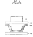
- FIG. 1 is a cross-sectional view illustrating a method of forming an organic layer pattern using an LITI method.
- a donor substrate 120 where an organic layer 130 is formed is laminated on a substrate 110 where a predetermined element is formed.
- a laser beam 150 is irradiated on a predetermined region of the donor substrate 120 having the organic layer 130
- the laser beam 150 is absorbed by a light-to-heat conversion layer of the donor substrate 120 and then converted to thermal energy, which allows the organic layer 130 forming a transfer layer to be transferred onto the substrate 110, thus patterning the organic layer on the substrate 110.
- the organic layer 130 is separated from the donor substrate 120 by the thermal energy, and is transferred onto the substrate 110 while bonding within the organic layer 130 is broken.
- Energy required to break the bonding within the organic layer 130 should be higher than energy required to allow the organic layer 130 to be broken from the donor substrate 120 and transferred. Dotted portion indicate portions where the bonding within the organic layer 130 is broken.
- FIGS. 2A and 2B are a schematic view and a beam profile illustrating a method of fabricating an organic light emitting display using a conventional laser irradiation apparatus.
- a laser irradiation apparatus 200 includes a laser generator 240, a patterned mask 260, and a projection lens 270.
- a laser beam 250 is irradiated from the laser generator 240 on a predetermined region in the donor substrate 120.
- the laser beam 250 irradiated from the laser generator 240 passes through the patterned mask 260 and refracted by the projection lens 270 to be irradiated on the donor substrate 120.
- the laser beam 250 is blocked at an unpatterned portion of the mask 260.
- the organic layer 130 on the donor substrate 120 is transferred on the substrate 110 by the laser beam 250. After the transfer process, a cathode is formed on the formed organic layer pattern to complete the organic light emitting display.
- a beam profile 280 of the laser beam 250 irradiated on the donor substrate 120 is illustrated.
- x-axis represents regions where the laser beam is irradiated, and y-axis represents intensity of the laser beam.
- the laser beam is irradiated over the irradiated region with uniform intensity.
- the intensity of the laser beam required to break the bonding in the organic layer 130 should be higher than that required to separate the organic layer 130 from the donor substrate 120 to be transferred on the substrate 110.
- the laser beam having excessive intensity to transfer the organic layer is irradiated on the organic layer so that the organic layer may be damaged to thereby degrade quality of the transferred organic layer pattern.
- the present invention therefore, solves aforementioned problems associated with conventional devices by providing the laser irradiation apparatus according to claim 1 and the method of fabricating an organic light emitting display according to claim 7, using a laser beam having low intensity and reducing damage for the transfer of an organic layer while forming an organic layer pattern using an LITI method, and improving quality of the transferred organic layer pattern.
- a transfer process can be performed using a laser beam having low intensity to improve quality of the transferred organic layer pattern.
- the means for changing the propagation path of the laser beam is a projection portion.
- the projection portion may be a lens, and the lens is preferably a convex lens.
- the convex lens may be formed at a lower or upper surface of the mask, or may be formed at the lower and upper surfaces.
- the projection portion may be polished to have a lens shape, and the lens shape is preferably polished to have a convex lens shape.
- the mask may be made of a transparent material, and the transparent material may use glass or plastic.
- the laser irradiation apparatus may irradiate the laser beam in a step-and-step manner.
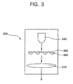
- FIG. 3 is a schematic view of a laser irradiation apparatus in accordance with the present invention.
- the laser irradiation apparatus 300 includes a laser generator 340, a mask 360 located under the laser generator 340 and having means for changing a propagation path of a laser beam, and a projection lens 370.
- the laser irradiation apparatus 300 may further include a beam shaping device disposed between the laser generator 340 and the patterned mask 360 to make the laser beam irradiated from the laser generator 340 uniform.
- a projection as means for changing a propagation path of a laser beam is formed at the mask 360, and a lens may be used as the projection.
- a convex lens is attached to the mask 360.
- the convex lens is attached to a lower surface of the mask 360. The propagation path of the laser beam irradiated from the laser generator 340 is refracted by the convex lens.
- a concave as means for changing a propagation path of a laser beam can be formed at the mask 360
- the mask may employ a transparent material.
- the mask may be made of transparent glass or plastic.
- the mask made of glass is used, and the mask is patterned using a material capable of blocking the laser beam.
- the present embodiment uses the mask made of glass, and uses the means 390 for changing the propagation path the a laser beam to irradiate the laser beam to a portion, at which the patterning is to be performed, without individually patterning the mask. That is, the laser beam passes through the portion, at which the means for changing propagation path of the laser beam is not formed, and the laser beam is refracted at the portion, which the means for changing propagation path of the laser beam is formed, thereby being introduced into the projection lens 370.
- the laser beam is irradiated through the means for changing a propagation path of a laser beam so that the laser beam blocked by the conventional mask can be used in the transfer process, thereby using the laser beam having low energy to perform the transfer process.
- the means 390 for changing the propagation path of the laser beam may employ various types, and their descriptions will be described in conjunction with FIGS. 4A to 4D .
- the laser irradiation apparatus 300 may irradiate the laser beam in a step-and-step manner. That is, the laser beam is irradiated using the laser irradiation apparatus 300 in one step, and then the laser irradiation apparatus 300 is moved to the next step to irradiate the laser beam on a predetermined region.
- FIGS. 4A to 4D are cross-sectional views illustrating various convex and masks having a convex lens shape included in a laser irradiation apparatus in accordance with the present invention.
- means 490 for changing a propagation path of a laser beam is formed on a mask 460 made of glass, convex lenses as the means 460 being attached to a top surface of the mask 460 made of glass.
- convex lenses as the means 460 for changing a propagation path of a laser beam are attached to a top surface and a bottom surface of the mask 460 made of glass.
- examples that the mask 460 is processed to have a convex lens shape as the means 490 for changing a propagation path of a laser beam are illustrated.
- FIG. 4C illustrates an example that a bottom surface of the mask is processed to have a convex lens shape
- FIG. 4D illustrates an example that a top surface and a bottom surface of the mask 460 are processed to have a convex lens shape.
- FIGS. 5A and 5B are a schematic view and a beam profile illustrating a method of fabricating an organic light emitting display using a laser irradiation apparatus in accordance with an embodiment of the present invention.
- a donor substrate 120 having an organic layer 130 is laminated on a substrate 110 having a pixel electrode.
- the laser irradiation apparatus 500 irradiates a laser beam on the donor substrate 120 to form an organic layer pattern on the substrate 110 having the pixel electrode.
- the laser beam is irradiated on an edge portion of an irradiated region on the donor substrate 120 with high intensity. That is, in order to break the bonding in the organic layer 130, the high intensity of laser beam is irradiated on the edge portion.
- the laser irradiation apparatus 500 includes a laser generator 540, a mask having means 590 for changing a propagation path of a laser beam, and a projection lens 570.
- the mask 560 may be made of glass. Convex lenses as the means 590 for changing the propagation path of the laser beam are attached to a bottom surface of the mask 560.
- the laser irradiation apparatus 500 is similar to the laser irradiation apparatus 300 shown in FIG. 3 .
- the laser generator 540 irradiates a laser beam 550 on a predetermined region of the donor substrate 120.
- the laser beam 550 irradiated from the laser generator 540 passes through the mask 560 made of glass.
- the laser beam straightly passes through the portion of the mask 560, at which the convex lens is not attached, and the laser beams 551, 552, 553 and 554 passed through the mask 560 are introduced into the projection lens 570.
- the laser beams 551, 552, 553 and 554 refracted by the projection lens 570 are irradiated on the donor substrate 120.
- the propagation path of the laser bean is refracted at the portion of the mask, at which the convex lens is attached, and the refracted laser beam passes through the projection lens 570 to be refracted and irradiated on the donor substrate 120.
- the laser beams 555 and 556 passed through the convex lenses are refracted by the convex lens to be introduced into the projection lens 570.
- the laser beams 555 and 556 introduced into the projection lens 570 are refracted through the projection lens 570 to be irradiated on the regions of the donor substrate 120, at which the laser beams 552 and 553 passed through the regions of the mask 560 without the convex lens are irradiated, respectively.
- the laser beams blocked by the conventional mask pattern are refracted, being not blocked, by the means for changing the propagation path of the laser beam to be used in the transfer process.
- the projection lens may include a plurality of lenses arranged in a various manner to refract the laser beam in various directions.
- a beam profile 580 of the laser beam irradiated on the donor substrate 120 is illustrated.
- x-axis represents regions where the laser beam is irradiated
- y-axis represents intensity of the laser beam.
- the laser beam is irradiated on the regions of the donor substrate 120 with irregular intensity, both edges of which have high beam intensity profiles. That is, the laser beams 555 and 556 passed through the convex lens formed at the mask 560 are refracted to be irradiated on the regions, at which the laser beams 552 and 553 passed through the portion of the mask 560 without the convex lens are irradiated, thereby having the high intensity profile.
- the laser beams in the region having the high intensity are used to break the bonding in the organic layer 130, and the laser beams in the region having the low intensity are used to separate the organic layer 130 from the donor substrate 120 to transfer the organic layer 130.
- intensity of the laser beam required to break the bonding in the organic layer should higher than that required to separate the organic layer 130 from the donor substrate 120 to transfer the organic layer 130.
- the laser beam having the intensity required to separate the organic layer 130 from the donor substrate 120 to transfer the organic layer 130 is irradiated on the donor substrate 120, since the laser beam is concentratedly irradiated on the edges of the region with high intensity, the laser beam can break the bonding in the organic layer 130 to separate the organic layer 130 from the donor substrate 120 to transfer the organic layer 130 onto the substrate. That is, by using the laser beam blocked by the conventional mask, the laser beam having low intensity can be used to form the organic layer pattern, thereby improving laser efficiency. In addition, since the laser beam having low intensity is irradiated on the organic layer, it is possible to reduce damage on the organic layer pattern to be formed owing to the laser beam.
- the transfer process of forming the organic layer using the LITI method may be performed in an N 2 atmosphere. Since the general air contains an oxygen component so that the transferred organic layer pattern may be oxidized, the transfer process is preferably performed in the nitrogen atmosphere without oxygen component.
- the transfer process may be performed in a vacuum atmosphere, especially, when the donor substrate is laminated on an entire surface of the substrate, it is advantageous to suppress bubble generation between the donor substrate and the substrate.
- the laser irradiation apparatus 300 may irradiate the laser beam 550 in a step-and-step manner. Looking into the manner, the laser beam 550 is irradiated using the laser irradiation apparatus 500 in one step to form the organic layer pattern, and then the laser irradiation apparatus 300 is moved to the next step to irradiate the laser beam 550 on a predetermined region to form another organic layer pattern. Repeating this process, the organic layer pattern may be formed in a desired shape.
- the organic layer pattern may be a single layer or a multi-layer of at least two layers selected from a group consisting of an emission layer, a hole injection layer, a hole transport layer, an electron transport layer, and an electron injection layer.
- a cathode is formed on the organic layer pattern to complete the organic light emitting display.
- the laser beam is irradiated through the mask having the means for changing a propagation path of a laser beam while forming the organic layer pattern using the LITI method.
- the laser beam having low intensity can perform the transfer process to improve laser beam efficiency.
Landscapes
- Engineering & Computer Science (AREA)
- Physics & Mathematics (AREA)
- Optics & Photonics (AREA)
- Manufacturing & Machinery (AREA)
- Plasma & Fusion (AREA)
- Mechanical Engineering (AREA)
- Electroluminescent Light Sources (AREA)
- Laser Beam Processing (AREA)
Claims (14)
- Laserbestrahlungsvorrichtung, aufweisend:einen Lasergenerator (540);ein transparentes optisches Glied (460, 560), das vor dem Lasergenerator angeordnet ist; undein Projektionsobjektiv, das auf einer dem Lasergenerator (540) gegenüberliegenden Seite des transparenten optischen Gliedes (460, 560) angeordnet ist,dadurch gekennzeichnet, dass das transparente optische Glied (460, 560) eine Vielzahl alternierender konvexer Teile (490, 590) zum Ändern eines Ausbreitungsweges eines vom Lasergenerator ausgestrahlten Laserstrahls sowie ebene Teile zur Weiterleitung des Laserstrahls aufweist,wobei die konvexen Teile (490, 590) auf einer Vorderfläche und/oder einer Rückfläche des transparenten optischen Gliedes (460, 560) ausgebildet sind.
- Laserbestrahlungsvorrichtung nach Anspruch 1, wobei die Entfernung zwischen dem transparenten optischen Glied (460, 560) und dem Projektionsobjektiv (570) kürzer als die Brennweite der konvexen Teile (490, 590) ist.
- Laserbestrahlungsvorrichtung nach Anspruch 1, wobei die konvexen Teile (490, 590) sowohl auf der Vorderfläche als auch auf der Rückfläche des transparenten optischen Gliedes (460, 560) ausgebildet sind.
- Laserbestrahlungsvorrichtung nach Anspruch 1, wobei die konvexen Teile (490, 590) derart bearbeitet sind, dass sie eine konvexe Linsenform aufweisen.
- Laserbestrahlungsvorrichtung nach Anspruch 1, wobei das transparente optische Glied (460, 560) aus Glas oder aus Kunststoff hergestellt ist.
- Laserbestrahlungsvorrichtung nach Anspruch 1, wobei die Laserbestrahlungsvorrichtung den Laserstrahl schrittweise ausstrahlt.
- Verfahren zur Herstellung einer organischen elektrolumineszenten Anzeigevorrichtung, aufweisend:Bereitstellung eines Substrats (110), das eine Pixelelektrode aufweist;Laminieren eines Donorsubstrats (120) auf eine gesamte Oberfläche des Substrats (110); undAusstrahlung eines Laserstrahls auf eine vorbestimmte Region des Donorsubstrats (120) mittels einer Laserbestrahlungsvorrichtung zur Ausbildung eines organischen Schichtmusters (130) auf dem Substrat (110),wobei die Laserbestrahlungsvorrichtung aufweist: einen Lasergenerator (540); ein transparentes optisches Glied (460, 560), das vor dem Lasergenerator (540) angeordnet ist; und ein Projektionsobjektiv (570), das auf einer dem Lasergenerator (540) gegenüberliegenden Seite des transparenten optischen Gliedes (460, 560) angeordnet ist;wobei das Verfahren dadurch gekennzeichnet ist, dass das transparente optische Glied (460, 560) konvexe Teile (490, 590) zur Brechung des Laserstrahls sowie ebene Teile zur Weiterleitung des Laserstrahls aufweist, undwobei die konvexen Teile (490, 590) auf einer Vorderfläche und/oder einer Rückfläche des transparenten optischen Gliedes (460, 560) ausgebildet sind, undwobei der Laserstrahl mit größerer Intensität auf einen Randbereich einer bestrahlten Region auf dem Donorsubstrat (120) als auf einen mittleren Bereich der bestrahlten Region gestrahlt wird, um die Verklebung in der zu übertragenden organischen Schicht (130) zu lösen.
- Verfahren nach Anspruch 7, wobei die konvexen Teile (490, 590) sowohl auf der Vorderfläche als auch auf der Rückfläche des transparenten optischen Gliedes (460, 560) ausgebildet sind.
- Verfahren nach Anspruch 7, wobei die konvexen Teile (490, 590) derart bearbeitet sind, dass sie eine konvexe Linsenform aufweisen.
- Verfahren nach Anspruch 7, wobei das transparente optische Glied (460, 560) aus Glas oder aus Kunststoff hergestellt wird.
- Verfahren nach Anspruch 7, wobei die Laserbestrahlungsvorrichtung den Laserstrahl schrittweise ausstrahlt.
- Verfahren nach Anspruch 7, wobei die Ausbildung des organischen Schichtmusters (130) auf der Pixelelektrode unter N2-Atmosphäre durchgeführt wird.
- Verfahren nach Anspruch 7, wobei die Ausbildung des organischen Schichtmusters (130) auf der Pixelelektrode unter Vakuum-Atmosphäre durchgefürht wird.
- Verfahren nach Anspruch 7, wobei das organische Schichtmuster (130) eine Einzelschicht oder eine aus zumindest zwei Schichten bestehende Mehrlagenschicht ist, und wobei die zumindest zwei Schichten aus einer Emissionsschicht, einer Lochinjektionsschicht, einer Lochtransportschicht, einer Elektronentransportschicht und einer Elektroneninjektionsschicht ausgewählt sind.
Applications Claiming Priority (1)
| Application Number | Priority Date | Filing Date | Title |
|---|---|---|---|
| KR1020040076666A KR100635569B1 (ko) | 2004-09-23 | 2004-09-23 | 레이저 조사 장치 및 그를 이용한 유기 전계 발광 소자의제조 방법 |
Publications (3)
| Publication Number | Publication Date |
|---|---|
| EP1640106A2 EP1640106A2 (de) | 2006-03-29 |
| EP1640106A3 EP1640106A3 (de) | 2006-06-07 |
| EP1640106B1 true EP1640106B1 (de) | 2008-10-15 |
Family
ID=36074455
Family Applications (1)
| Application Number | Title | Priority Date | Filing Date |
|---|---|---|---|
| EP04090519A Expired - Lifetime EP1640106B1 (de) | 2004-09-23 | 2004-12-29 | Laser-Bestrahlungsvorrichtung und Herstellungsmethode einer organischen elektrolumineszenten Anzeigevorrichtung |
Country Status (6)
| Country | Link |
|---|---|
| US (2) | US7525563B2 (de) |
| EP (1) | EP1640106B1 (de) |
| JP (1) | JP4554353B2 (de) |
| KR (1) | KR100635569B1 (de) |
| CN (1) | CN100459819C (de) |
| DE (1) | DE602004017177D1 (de) |
Families Citing this family (18)
| Publication number | Priority date | Publication date | Assignee | Title |
|---|---|---|---|---|
| KR100712115B1 (ko) * | 2004-09-21 | 2007-04-27 | 삼성에스디아이 주식회사 | 레이저 조사 장치 및 그를 이용한 유기 전계 발광 소자의제조 방법 |
| KR100635569B1 (ko) * | 2004-09-23 | 2006-10-17 | 삼성에스디아이 주식회사 | 레이저 조사 장치 및 그를 이용한 유기 전계 발광 소자의제조 방법 |
| KR100711878B1 (ko) * | 2005-08-30 | 2007-04-25 | 삼성에스디아이 주식회사 | 레이저 열 전사 장치 및 레이저 열 전사 방법 |
| US7817175B2 (en) | 2005-08-30 | 2010-10-19 | Samsung Mobile Display Co., Ltd. | Laser induced thermal imaging apparatus and fabricating method of organic light emitting diode using the same |
| JP2007062354A (ja) * | 2005-08-30 | 2007-03-15 | Samsung Sdi Co Ltd | レーザ熱転写ドナーフィルム、レーザ熱転写装置、レーザ熱転写法及び有機発光素子の製造方法 |
| JP2007128845A (ja) * | 2005-11-04 | 2007-05-24 | Samsung Sdi Co Ltd | レーザ熱転写装置及びレーザ熱転写方法 |
| JP2007128844A (ja) * | 2005-11-04 | 2007-05-24 | Samsung Sdi Co Ltd | レーザ熱転写装置及びレーザ熱転写方法そしてこれを利用した有機発光表示素子 |
| KR100782467B1 (ko) * | 2006-05-22 | 2007-12-05 | 삼성에스디아이 주식회사 | 레이저 조사장치 및 그를 이용한 유기전계발광소자의제조방법 |
| KR100782466B1 (ko) * | 2006-05-22 | 2007-12-05 | 삼성에스디아이 주식회사 | 레이저 조사장치 및 그를 이용한 유기전계발광소자의제조방법 |
| KR100782468B1 (ko) * | 2006-05-22 | 2007-12-05 | 삼성에스디아이 주식회사 | 레이저 조사장치 및 그를 이용한 유기전계발광소자의제조방법 |
| KR100782470B1 (ko) * | 2006-05-22 | 2007-12-05 | 삼성에스디아이 주식회사 | 레이저 조사장치 및 그를 이용한 유기전계발광소자의제조방법 |
| KR100782469B1 (ko) * | 2006-05-22 | 2007-12-05 | 삼성에스디아이 주식회사 | 레이저 조사장치 및 그를 이용한 유기전계발광소자의제조방법. |
| JP5386790B2 (ja) * | 2007-03-30 | 2014-01-15 | 富士ゼロックス株式会社 | 露光装置および画像形成装置 |
| KR100989130B1 (ko) | 2008-08-19 | 2010-10-20 | 삼성모바일디스플레이주식회사 | 레이저 조사 장치 및 그를 이용한 유기전계발광표시장치의 제조 방법 |
| CN102239582B (zh) * | 2008-12-05 | 2015-08-12 | 皇家飞利浦电子股份有限公司 | 图案化led器件、生成图案化的方法、用于图案化的系统和校准该系统的方法 |
| JP5695337B2 (ja) * | 2010-04-16 | 2015-04-01 | 株式会社半導体エネルギー研究所 | レーザ照射装置 |
| KR20140133741A (ko) * | 2013-05-10 | 2014-11-20 | 삼성디스플레이 주식회사 | 레이저 열전사용 마스크 및 이를 포함하는 레이저 조사 장치 |
| KR20150109013A (ko) | 2014-03-18 | 2015-10-01 | 삼성디스플레이 주식회사 | 유기막 패턴 형성용 마스크, 이를 이용한 유기막 패턴 형성 방법 및 유기 발광 표시 장치의 제조 방법 |
Family Cites Families (21)
| Publication number | Priority date | Publication date | Assignee | Title |
|---|---|---|---|---|
| DE3607928A1 (de) | 1986-03-11 | 1987-09-17 | Thomson Brandt Gmbh | Schaltung zur digitalen kompensation eines determinierten stoersignals |
| JP2657957B2 (ja) | 1990-04-27 | 1997-09-30 | キヤノン株式会社 | 投影装置及び光照射方法 |
| KR940000798B1 (ko) | 1991-05-14 | 1994-01-31 | 주식회사 하이게인 안테나 | 빔 틸트형 전방향성 안테나 |
| DE4143066A1 (de) | 1991-12-27 | 1993-07-01 | Jenoptik Jena Gmbh | Verfahren und anordnung zum markieren von oberflaechen |
| KR960001876B1 (en) | 1994-04-26 | 1996-02-06 | Daewoo Motor Co Ltd | Impact beam of a car |
| US5521035A (en) * | 1994-07-11 | 1996-05-28 | Minnesota Mining And Manufacturing Company | Methods for preparing color filter elements using laser induced transfer of colorants with associated liquid crystal display device |
| KR19980023069A (ko) | 1996-09-25 | 1998-07-06 | 문정환 | 마이크로 렌즈형 마스크 및 그 제조 방법 |
| DE19841040A1 (de) * | 1997-09-10 | 1999-03-11 | Alltec Angewandte Laser Licht | Vorrichtung zum Markieren einer Oberfläche mittels Laserstrahlen |
| JPH11354271A (ja) * | 1998-06-05 | 1999-12-24 | Canon Inc | 感光材料書込み装置 |
| US6661445B2 (en) * | 1998-08-31 | 2003-12-09 | Canon Kabushiki Kaisha | Exposure apparatus with an array of light emitting devices |
| KR100342653B1 (ko) | 2000-08-24 | 2002-07-03 | 김순택 | 유기 전계발광소자의 제조 방법 |
| US6358664B1 (en) | 2000-09-15 | 2002-03-19 | 3M Innovative Properties Company | Electronically active primer layers for thermal patterning of materials for electronic devices |
| JP4766218B2 (ja) * | 2001-07-09 | 2011-09-07 | セイコーエプソン株式会社 | 有機elアレイ露光ヘッドとその作製方法及びそれを用いた画像形成装置 |
| JP3903761B2 (ja) * | 2001-10-10 | 2007-04-11 | 株式会社日立製作所 | レ−ザアニ−ル方法およびレ−ザアニ−ル装置 |
| US6688365B2 (en) | 2001-12-19 | 2004-02-10 | Eastman Kodak Company | Method for transferring of organic material from a donor to form a layer in an OLED device |
| US6582875B1 (en) | 2002-01-23 | 2003-06-24 | Eastman Kodak Company | Using a multichannel linear laser light beam in making OLED devices by thermal transfer |
| DE60318145T2 (de) * | 2002-03-11 | 2008-12-24 | Seiko Epson Corp. | Optischer Schreibkopf wie organische elektrolumineszente Belichtungskopf-Matrizen, Verfahren zu dessen Herstellung und Bilderzeugungsvorrichtung, die diesen nutzt |
| JP4158514B2 (ja) * | 2002-12-24 | 2008-10-01 | ウシオ電機株式会社 | 両面投影露光装置 |
| KR100698056B1 (ko) * | 2003-12-26 | 2007-03-23 | 엘지.필립스 엘시디 주식회사 | 레이저 빔 패턴 마스크 및 이를 이용한 결정화 방법 |
| JP2006103307A (ja) * | 2004-09-07 | 2006-04-20 | Seiko Epson Corp | ラインヘッドモジュール及び画像形成装置 |
| KR100635569B1 (ko) * | 2004-09-23 | 2006-10-17 | 삼성에스디아이 주식회사 | 레이저 조사 장치 및 그를 이용한 유기 전계 발광 소자의제조 방법 |
-
2004
- 2004-09-23 KR KR1020040076666A patent/KR100635569B1/ko not_active Expired - Lifetime
- 2004-12-27 US US11/020,659 patent/US7525563B2/en active Active
- 2004-12-27 JP JP2004377845A patent/JP4554353B2/ja not_active Expired - Lifetime
- 2004-12-29 DE DE602004017177T patent/DE602004017177D1/de not_active Expired - Lifetime
- 2004-12-29 EP EP04090519A patent/EP1640106B1/de not_active Expired - Lifetime
- 2004-12-31 CN CNB2004100820685A patent/CN100459819C/zh not_active Expired - Lifetime
-
2009
- 2009-03-18 US US12/406,640 patent/US7999835B2/en not_active Expired - Lifetime
Also Published As
| Publication number | Publication date |
|---|---|
| EP1640106A2 (de) | 2006-03-29 |
| US7999835B2 (en) | 2011-08-16 |
| CN100459819C (zh) | 2009-02-04 |
| US7525563B2 (en) | 2009-04-28 |
| JP4554353B2 (ja) | 2010-09-29 |
| EP1640106A3 (de) | 2006-06-07 |
| KR20060027742A (ko) | 2006-03-28 |
| US20090181328A1 (en) | 2009-07-16 |
| US20060063096A1 (en) | 2006-03-23 |
| CN1753584A (zh) | 2006-03-29 |
| KR100635569B1 (ko) | 2006-10-17 |
| DE602004017177D1 (de) | 2008-11-27 |
| JP2006093077A (ja) | 2006-04-06 |
Similar Documents
| Publication | Publication Date | Title |
|---|---|---|
| US7999835B2 (en) | Laser irradiation apparatus and method of fabricating organic light emitting display using the same | |
| US7675003B2 (en) | Laser irradiation device, patterning method and method of fabricating organic light emitting display (OLED) using the patterning method | |
| US7999839B2 (en) | Laser irradiation apparatus and method of fabricating organic light emitting display using the same | |
| US8741535B2 (en) | Laser irradiation device and method of fabricating organic light emitting display device using the same | |
| JP5663262B2 (ja) | レーザ熱転写方法、それを用いた有機膜パターニング方法及び有機電界発光表示装置の製造方法 | |
| KR100700654B1 (ko) | 레이저 조사 장치 및 레이저 열 전사법 | |
| JP2006093127A (ja) | 有機電界発光素子の製造方法 | |
| JP2007053092A (ja) | レーザー熱転写用マスク及びこれを用いた有機電界発光素子の製造方法 | |
| JPH06326337A (ja) | レーザ加工装置 | |
| US7303850B2 (en) | Method of fabricating organic light emitting display | |
| KR20070112678A (ko) | 레이저 조사장치 및 그를 이용한 유기전계발광소자의제조방법. |
Legal Events
| Date | Code | Title | Description |
|---|---|---|---|
| PUAI | Public reference made under article 153(3) epc to a published international application that has entered the european phase |
Free format text: ORIGINAL CODE: 0009012 |
|
| 17P | Request for examination filed |
Effective date: 20050126 |
|
| AK | Designated contracting states |
Kind code of ref document: A2 Designated state(s): AT BE BG CH CY CZ DE DK EE ES FI FR GB GR HU IE IS IT LI LT LU MC NL PL PT RO SE SI SK TR |
|
| AX | Request for extension of the european patent |
Extension state: AL BA HR LV MK YU |
|
| PUAL | Search report despatched |
Free format text: ORIGINAL CODE: 0009013 |
|
| AK | Designated contracting states |
Kind code of ref document: A3 Designated state(s): AT BE BG CH CY CZ DE DK EE ES FI FR GB GR HU IE IS IT LI LT LU MC NL PL PT RO SE SI SK TR |
|
| AX | Request for extension of the european patent |
Extension state: AL BA HR LV MK YU |
|
| 17Q | First examination report despatched |
Effective date: 20060828 |
|
| AKX | Designation fees paid |
Designated state(s): DE FR GB |
|
| GRAP | Despatch of communication of intention to grant a patent |
Free format text: ORIGINAL CODE: EPIDOSNIGR1 |
|
| GRAS | Grant fee paid |
Free format text: ORIGINAL CODE: EPIDOSNIGR3 |
|
| GRAA | (expected) grant |
Free format text: ORIGINAL CODE: 0009210 |
|
| AK | Designated contracting states |
Kind code of ref document: B1 Designated state(s): DE FR GB |
|
| REG | Reference to a national code |
Ref country code: GB Ref legal event code: FG4D |
|
| REF | Corresponds to: |
Ref document number: 602004017177 Country of ref document: DE Date of ref document: 20081127 Kind code of ref document: P |
|
| REG | Reference to a national code |
Ref country code: DE Ref legal event code: R096 Ref document number: 602004017177 Country of ref document: DE Effective date: 20081127 |
|
| REG | Reference to a national code |
Ref country code: GB Ref legal event code: 732E |
|
| REG | Reference to a national code |
Ref country code: DE Ref legal event code: R081 Ref document number: 602004017177 Country of ref document: DE Owner name: SAMSUNG DISPLAY CO., LTD., YONGIN-CITY, KR Free format text: FORMER OWNER: SAMSUNG SDI CO., LTD., SUWON, KYONGGI-DO, KR Effective date: 20090401 |
|
| PLBE | No opposition filed within time limit |
Free format text: ORIGINAL CODE: 0009261 |
|
| STAA | Information on the status of an ep patent application or granted ep patent |
Free format text: STATUS: NO OPPOSITION FILED WITHIN TIME LIMIT |
|
| 26N | No opposition filed |
Effective date: 20090716 |
|
| REG | Reference to a national code |
Ref country code: DE Ref legal event code: R097 Ref document number: 602004017177 Country of ref document: DE Effective date: 20090716 |
|
| REG | Reference to a national code |
Ref country code: DE Ref legal event code: R082 Ref document number: 602004017177 Country of ref document: DE Representative=s name: GULDE HENGELHAUPT ZIEBIG & SCHNEIDER, DE |
|
| REG | Reference to a national code |
Ref country code: DE Ref legal event code: R082 Ref document number: 602004017177 Country of ref document: DE Representative=s name: GULDE HENGELHAUPT ZIEBIG & SCHNEIDER, DE Effective date: 20121026 Ref country code: DE Ref legal event code: R081 Ref document number: 602004017177 Country of ref document: DE Owner name: SAMSUNG DISPLAY CO., LTD., KR Free format text: FORMER OWNER: SAMSUNG MOBILE DISPLAY CO. LTD., SUWON, KR Effective date: 20121026 Ref country code: DE Ref legal event code: R081 Ref document number: 602004017177 Country of ref document: DE Owner name: SAMSUNG DISPLAY CO., LTD., YONGIN-CITY, KR Free format text: FORMER OWNER: SAMSUNG MOBILE DISPLAY CO. LTD., SUWON, GYEONGGI, KR Effective date: 20121026 Ref country code: DE Ref legal event code: R082 Ref document number: 602004017177 Country of ref document: DE Representative=s name: GULDE & PARTNER PATENT- UND RECHTSANWALTSKANZL, DE Effective date: 20121026 |
|
| REG | Reference to a national code |
Ref country code: GB Ref legal event code: 732E Free format text: REGISTERED BETWEEN 20130103 AND 20130109 |
|
| REG | Reference to a national code |
Ref country code: FR Ref legal event code: PLFP Year of fee payment: 12 |
|
| REG | Reference to a national code |
Ref country code: FR Ref legal event code: PLFP Year of fee payment: 13 |
|
| REG | Reference to a national code |
Ref country code: FR Ref legal event code: PLFP Year of fee payment: 14 |
|
| P01 | Opt-out of the competence of the unified patent court (upc) registered |
Effective date: 20230516 |
|
| PGFP | Annual fee paid to national office [announced via postgrant information from national office to epo] |
Ref country code: GB Payment date: 20231120 Year of fee payment: 20 |
|
| PGFP | Annual fee paid to national office [announced via postgrant information from national office to epo] |
Ref country code: FR Payment date: 20231121 Year of fee payment: 20 Ref country code: DE Payment date: 20231120 Year of fee payment: 20 |
|
| REG | Reference to a national code |
Ref country code: DE Ref legal event code: R071 Ref document number: 602004017177 Country of ref document: DE |
|
| PG25 | Lapsed in a contracting state [announced via postgrant information from national office to epo] |
Ref country code: GB Free format text: LAPSE BECAUSE OF EXPIRATION OF PROTECTION Effective date: 20241228 |
|
| REG | Reference to a national code |
Ref country code: GB Ref legal event code: PE20 Expiry date: 20241228 |
|
| PG25 | Lapsed in a contracting state [announced via postgrant information from national office to epo] |
Ref country code: GB Free format text: LAPSE BECAUSE OF EXPIRATION OF PROTECTION Effective date: 20241228 |