EP1639634B1 - Elektronische vorrichtung, anordnung und verfahren zum herstellen einer elektronischen vorrichtung - Google Patents
Elektronische vorrichtung, anordnung und verfahren zum herstellen einer elektronischen vorrichtung Download PDFInfo
- Publication number
- EP1639634B1 EP1639634B1 EP04736684A EP04736684A EP1639634B1 EP 1639634 B1 EP1639634 B1 EP 1639634B1 EP 04736684 A EP04736684 A EP 04736684A EP 04736684 A EP04736684 A EP 04736684A EP 1639634 B1 EP1639634 B1 EP 1639634B1
- Authority
- EP
- European Patent Office
- Prior art keywords
- trenches
- substrate
- capacitor
- electronic device
- layer
- Prior art date
- Legal status (The legal status is an assumption and is not a legal conclusion. Google has not performed a legal analysis and makes no representation as to the accuracy of the status listed.)
- Expired - Lifetime
Links
Images


Classifications
-
- H—ELECTRICITY
- H10—SEMICONDUCTOR DEVICES; ELECTRIC SOLID-STATE DEVICES NOT OTHERWISE PROVIDED FOR
- H10D—INORGANIC ELECTRIC SEMICONDUCTOR DEVICES
- H10D1/00—Resistors, capacitors or inductors
- H10D1/60—Capacitors
- H10D1/68—Capacitors having no potential barriers
- H10D1/692—Electrodes
- H10D1/711—Electrodes having non-planar surfaces, e.g. formed by texturisation
- H10D1/716—Electrodes having non-planar surfaces, e.g. formed by texturisation having vertical extensions
-
- H—ELECTRICITY
- H10—SEMICONDUCTOR DEVICES; ELECTRIC SOLID-STATE DEVICES NOT OTHERWISE PROVIDED FOR
- H10W—GENERIC PACKAGES, INTERCONNECTIONS, CONNECTORS OR OTHER CONSTRUCTIONAL DETAILS OF DEVICES COVERED BY CLASS H10
- H10W76/00—Containers; Fillings or auxiliary members therefor; Seals
- H10W76/10—Containers or parts thereof
-
- H—ELECTRICITY
- H10—SEMICONDUCTOR DEVICES; ELECTRIC SOLID-STATE DEVICES NOT OTHERWISE PROVIDED FOR
- H10W—GENERIC PACKAGES, INTERCONNECTIONS, CONNECTORS OR OTHER CONSTRUCTIONAL DETAILS OF DEVICES COVERED BY CLASS H10
- H10W44/00—Electrical arrangements for controlling or matching impedance
- H10W44/20—Electrical arrangements for controlling or matching impedance at high-frequency [HF] or radio frequency [RF]
-
- H—ELECTRICITY
- H10—SEMICONDUCTOR DEVICES; ELECTRIC SOLID-STATE DEVICES NOT OTHERWISE PROVIDED FOR
- H10D—INORGANIC ELECTRIC SEMICONDUCTOR DEVICES
- H10D1/00—Resistors, capacitors or inductors
- H10D1/01—Manufacture or treatment
- H10D1/045—Manufacture or treatment of capacitors having potential barriers, e.g. varactors
- H10D1/047—Manufacture or treatment of capacitors having potential barriers, e.g. varactors of conductor-insulator-semiconductor capacitors, e.g. trench capacitors
-
- H—ELECTRICITY
- H10—SEMICONDUCTOR DEVICES; ELECTRIC SOLID-STATE DEVICES NOT OTHERWISE PROVIDED FOR
- H10D—INORGANIC ELECTRIC SEMICONDUCTOR DEVICES
- H10D1/00—Resistors, capacitors or inductors
- H10D1/60—Capacitors
- H10D1/62—Capacitors having potential barriers
- H10D1/66—Conductor-insulator-semiconductor capacitors, e.g. MOS capacitors
- H10D1/665—Trench conductor-insulator-semiconductor capacitors, e.g. trench MOS capacitors
-
- H—ELECTRICITY
- H10—SEMICONDUCTOR DEVICES; ELECTRIC SOLID-STATE DEVICES NOT OTHERWISE PROVIDED FOR
- H10D—INORGANIC ELECTRIC SEMICONDUCTOR DEVICES
- H10D1/00—Resistors, capacitors or inductors
- H10D1/60—Capacitors
- H10D1/68—Capacitors having no potential barriers
- H10D1/692—Electrodes
-
- H—ELECTRICITY
- H10—SEMICONDUCTOR DEVICES; ELECTRIC SOLID-STATE DEVICES NOT OTHERWISE PROVIDED FOR
- H10D—INORGANIC ELECTRIC SEMICONDUCTOR DEVICES
- H10D62/00—Semiconductor bodies, or regions thereof, of devices having potential barriers
- H10D62/10—Shapes, relative sizes or dispositions of the regions of the semiconductor bodies; Shapes of the semiconductor bodies
- H10D62/117—Shapes of semiconductor bodies
-
- H—ELECTRICITY
- H10—SEMICONDUCTOR DEVICES; ELECTRIC SOLID-STATE DEVICES NOT OTHERWISE PROVIDED FOR
- H10D—INORGANIC ELECTRIC SEMICONDUCTOR DEVICES
- H10D84/00—Integrated devices formed in or on semiconductor substrates that comprise only semiconducting layers, e.g. on Si wafers or on GaAs-on-Si wafers
- H10D84/201—Integrated devices formed in or on semiconductor substrates that comprise only semiconducting layers, e.g. on Si wafers or on GaAs-on-Si wafers characterised by the integration of only components covered by H10D1/00 or H10D8/00, e.g. RLC circuits
- H10D84/204—Integrated devices formed in or on semiconductor substrates that comprise only semiconducting layers, e.g. on Si wafers or on GaAs-on-Si wafers characterised by the integration of only components covered by H10D1/00 or H10D8/00, e.g. RLC circuits of combinations of diodes or capacitors or resistors
- H10D84/212—Integrated devices formed in or on semiconductor substrates that comprise only semiconducting layers, e.g. on Si wafers or on GaAs-on-Si wafers characterised by the integration of only components covered by H10D1/00 or H10D8/00, e.g. RLC circuits of combinations of diodes or capacitors or resistors of only capacitors
-
- H—ELECTRICITY
- H10—SEMICONDUCTOR DEVICES; ELECTRIC SOLID-STATE DEVICES NOT OTHERWISE PROVIDED FOR
- H10W—GENERIC PACKAGES, INTERCONNECTIONS, CONNECTORS OR OTHER CONSTRUCTIONAL DETAILS OF DEVICES COVERED BY CLASS H10
- H10W20/00—Interconnections in chips, wafers or substrates
- H10W20/01—Manufacture or treatment
- H10W20/021—Manufacture or treatment of interconnections within wafers or substrates
- H10W20/023—Manufacture or treatment of interconnections within wafers or substrates the interconnections being through-semiconductor vias
- H10W20/0242—Manufacture or treatment of interconnections within wafers or substrates the interconnections being through-semiconductor vias comprising etching via holes from the back sides of the chips, wafers or substrates
-
- H—ELECTRICITY
- H10—SEMICONDUCTOR DEVICES; ELECTRIC SOLID-STATE DEVICES NOT OTHERWISE PROVIDED FOR
- H10W—GENERIC PACKAGES, INTERCONNECTIONS, CONNECTORS OR OTHER CONSTRUCTIONAL DETAILS OF DEVICES COVERED BY CLASS H10
- H10W20/00—Interconnections in chips, wafers or substrates
- H10W20/01—Manufacture or treatment
- H10W20/021—Manufacture or treatment of interconnections within wafers or substrates
- H10W20/023—Manufacture or treatment of interconnections within wafers or substrates the interconnections being through-semiconductor vias
- H10W20/0245—Manufacture or treatment of interconnections within wafers or substrates the interconnections being through-semiconductor vias comprising use of blind vias during the manufacture
-
- H—ELECTRICITY
- H10—SEMICONDUCTOR DEVICES; ELECTRIC SOLID-STATE DEVICES NOT OTHERWISE PROVIDED FOR
- H10W—GENERIC PACKAGES, INTERCONNECTIONS, CONNECTORS OR OTHER CONSTRUCTIONAL DETAILS OF DEVICES COVERED BY CLASS H10
- H10W20/00—Interconnections in chips, wafers or substrates
- H10W20/20—Interconnections within wafers or substrates, e.g. through-silicon vias [TSV]
- H10W20/211—Through-semiconductor vias, e.g. TSVs
- H10W20/212—Top-view shapes or dispositions, e.g. top-view layouts of the vias
- H10W20/2125—Top-view shapes
-
- H—ELECTRICITY
- H10—SEMICONDUCTOR DEVICES; ELECTRIC SOLID-STATE DEVICES NOT OTHERWISE PROVIDED FOR
- H10W—GENERIC PACKAGES, INTERCONNECTIONS, CONNECTORS OR OTHER CONSTRUCTIONAL DETAILS OF DEVICES COVERED BY CLASS H10
- H10W70/00—Package substrates; Interposers; Redistribution layers [RDL]
- H10W70/01—Manufacture or treatment
- H10W70/05—Manufacture or treatment of insulating or insulated package substrates, or of interposers, or of redistribution layers
- H10W70/095—Manufacture or treatment of insulating or insulated package substrates, or of interposers, or of redistribution layers of vias therein
-
- H—ELECTRICITY
- H10—SEMICONDUCTOR DEVICES; ELECTRIC SOLID-STATE DEVICES NOT OTHERWISE PROVIDED FOR
- H10W—GENERIC PACKAGES, INTERCONNECTIONS, CONNECTORS OR OTHER CONSTRUCTIONAL DETAILS OF DEVICES COVERED BY CLASS H10
- H10W70/00—Package substrates; Interposers; Redistribution layers [RDL]
- H10W70/60—Insulating or insulated package substrates; Interposers; Redistribution layers
- H10W70/62—Insulating or insulated package substrates; Interposers; Redistribution layers characterised by their interconnections
- H10W70/63—Vias, e.g. via plugs
- H10W70/635—Through-vias
-
- H—ELECTRICITY
- H10—SEMICONDUCTOR DEVICES; ELECTRIC SOLID-STATE DEVICES NOT OTHERWISE PROVIDED FOR
- H10W—GENERIC PACKAGES, INTERCONNECTIONS, CONNECTORS OR OTHER CONSTRUCTIONAL DETAILS OF DEVICES COVERED BY CLASS H10
- H10W70/00—Package substrates; Interposers; Redistribution layers [RDL]
- H10W70/60—Insulating or insulated package substrates; Interposers; Redistribution layers
- H10W70/62—Insulating or insulated package substrates; Interposers; Redistribution layers characterised by their interconnections
- H10W70/65—Shapes or dispositions of interconnections
-
- H—ELECTRICITY
- H10—SEMICONDUCTOR DEVICES; ELECTRIC SOLID-STATE DEVICES NOT OTHERWISE PROVIDED FOR
- H10W—GENERIC PACKAGES, INTERCONNECTIONS, CONNECTORS OR OTHER CONSTRUCTIONAL DETAILS OF DEVICES COVERED BY CLASS H10
- H10W70/00—Package substrates; Interposers; Redistribution layers [RDL]
- H10W70/60—Insulating or insulated package substrates; Interposers; Redistribution layers
- H10W70/62—Insulating or insulated package substrates; Interposers; Redistribution layers characterised by their interconnections
- H10W70/66—Conductive materials thereof
- H10W70/662—Semiconductor materials
-
- H—ELECTRICITY
- H10—SEMICONDUCTOR DEVICES; ELECTRIC SOLID-STATE DEVICES NOT OTHERWISE PROVIDED FOR
- H10W—GENERIC PACKAGES, INTERCONNECTIONS, CONNECTORS OR OTHER CONSTRUCTIONAL DETAILS OF DEVICES COVERED BY CLASS H10
- H10W90/00—Package configurations
-
- H—ELECTRICITY
- H10—SEMICONDUCTOR DEVICES; ELECTRIC SOLID-STATE DEVICES NOT OTHERWISE PROVIDED FOR
- H10W—GENERIC PACKAGES, INTERCONNECTIONS, CONNECTORS OR OTHER CONSTRUCTIONAL DETAILS OF DEVICES COVERED BY CLASS H10
- H10W44/00—Electrical arrangements for controlling or matching impedance
- H10W44/20—Electrical arrangements for controlling or matching impedance at high-frequency [HF] or radio frequency [RF]
- H10W44/203—Electrical connections
- H10W44/209—Vertical interconnections, e.g. vias
- H10W44/212—Coaxial feed-throughs in substrates
-
- H—ELECTRICITY
- H10—SEMICONDUCTOR DEVICES; ELECTRIC SOLID-STATE DEVICES NOT OTHERWISE PROVIDED FOR
- H10W—GENERIC PACKAGES, INTERCONNECTIONS, CONNECTORS OR OTHER CONSTRUCTIONAL DETAILS OF DEVICES COVERED BY CLASS H10
- H10W44/00—Electrical arrangements for controlling or matching impedance
- H10W44/20—Electrical arrangements for controlling or matching impedance at high-frequency [HF] or radio frequency [RF]
- H10W44/241—Electrical arrangements for controlling or matching impedance at high-frequency [HF] or radio frequency [RF] for passive devices or passive elements
- H10W44/243—Electrical arrangements for controlling or matching impedance at high-frequency [HF] or radio frequency [RF] for passive devices or passive elements for decoupling, e.g. bypass capacitors
-
- H—ELECTRICITY
- H10—SEMICONDUCTOR DEVICES; ELECTRIC SOLID-STATE DEVICES NOT OTHERWISE PROVIDED FOR
- H10W—GENERIC PACKAGES, INTERCONNECTIONS, CONNECTORS OR OTHER CONSTRUCTIONAL DETAILS OF DEVICES COVERED BY CLASS H10
- H10W72/00—Interconnections or connectors in packages
- H10W72/823—Interconnections through encapsulations, e.g. pillars through molded resin on a lateral side a chip
-
- H—ELECTRICITY
- H10—SEMICONDUCTOR DEVICES; ELECTRIC SOLID-STATE DEVICES NOT OTHERWISE PROVIDED FOR
- H10W—GENERIC PACKAGES, INTERCONNECTIONS, CONNECTORS OR OTHER CONSTRUCTIONAL DETAILS OF DEVICES COVERED BY CLASS H10
- H10W72/00—Interconnections or connectors in packages
- H10W72/90—Bond pads, in general
- H10W72/921—Structures or relative sizes of bond pads
- H10W72/922—Bond pads being integral with underlying chip-level interconnections
- H10W72/9226—Bond pads being integral with underlying chip-level interconnections with via interconnections
-
- H—ELECTRICITY
- H10—SEMICONDUCTOR DEVICES; ELECTRIC SOLID-STATE DEVICES NOT OTHERWISE PROVIDED FOR
- H10W—GENERIC PACKAGES, INTERCONNECTIONS, CONNECTORS OR OTHER CONSTRUCTIONAL DETAILS OF DEVICES COVERED BY CLASS H10
- H10W72/00—Interconnections or connectors in packages
- H10W72/90—Bond pads, in general
- H10W72/921—Structures or relative sizes of bond pads
- H10W72/923—Bond pads having multiple stacked layers
-
- H—ELECTRICITY
- H10—SEMICONDUCTOR DEVICES; ELECTRIC SOLID-STATE DEVICES NOT OTHERWISE PROVIDED FOR
- H10W—GENERIC PACKAGES, INTERCONNECTIONS, CONNECTORS OR OTHER CONSTRUCTIONAL DETAILS OF DEVICES COVERED BY CLASS H10
- H10W72/00—Interconnections or connectors in packages
- H10W72/90—Bond pads, in general
- H10W72/941—Dispositions of bond pads
- H10W72/9415—Dispositions of bond pads relative to the surface, e.g. recessed, protruding
-
- H—ELECTRICITY
- H10—SEMICONDUCTOR DEVICES; ELECTRIC SOLID-STATE DEVICES NOT OTHERWISE PROVIDED FOR
- H10W—GENERIC PACKAGES, INTERCONNECTIONS, CONNECTORS OR OTHER CONSTRUCTIONAL DETAILS OF DEVICES COVERED BY CLASS H10
- H10W72/00—Interconnections or connectors in packages
- H10W72/90—Bond pads, in general
- H10W72/941—Dispositions of bond pads
- H10W72/942—Dispositions of bond pads relative to underlying supporting features, e.g. bond pads, RDLs or vias
-
- H—ELECTRICITY
- H10—SEMICONDUCTOR DEVICES; ELECTRIC SOLID-STATE DEVICES NOT OTHERWISE PROVIDED FOR
- H10W—GENERIC PACKAGES, INTERCONNECTIONS, CONNECTORS OR OTHER CONSTRUCTIONAL DETAILS OF DEVICES COVERED BY CLASS H10
- H10W90/00—Package configurations
- H10W90/20—Configurations of stacked chips
- H10W90/22—Configurations of stacked chips the stacked chips being on both top and bottom sides of a package substrate, interposer or RDL
-
- H—ELECTRICITY
- H10—SEMICONDUCTOR DEVICES; ELECTRIC SOLID-STATE DEVICES NOT OTHERWISE PROVIDED FOR
- H10W—GENERIC PACKAGES, INTERCONNECTIONS, CONNECTORS OR OTHER CONSTRUCTIONAL DETAILS OF DEVICES COVERED BY CLASS H10
- H10W90/00—Package configurations
- H10W90/701—Package configurations characterised by the relative positions of pads or connectors relative to package parts
- H10W90/721—Package configurations characterised by the relative positions of pads or connectors relative to package parts of bump connectors
- H10W90/724—Package configurations characterised by the relative positions of pads or connectors relative to package parts of bump connectors between a chip and a stacked insulating package substrate, interposer or RDL
-
- H—ELECTRICITY
- H10—SEMICONDUCTOR DEVICES; ELECTRIC SOLID-STATE DEVICES NOT OTHERWISE PROVIDED FOR
- H10W—GENERIC PACKAGES, INTERCONNECTIONS, CONNECTORS OR OTHER CONSTRUCTIONAL DETAILS OF DEVICES COVERED BY CLASS H10
- H10W90/00—Package configurations
- H10W90/701—Package configurations characterised by the relative positions of pads or connectors relative to package parts
- H10W90/721—Package configurations characterised by the relative positions of pads or connectors relative to package parts of bump connectors
- H10W90/728—Package configurations characterised by the relative positions of pads or connectors relative to package parts of bump connectors between a chip and a stacked discrete passive device, e.g. resistors, capacitors or inductors
Definitions
- the invention relates to an electronic device comprising a semiconductor substrate having a first and a second side and provided with a capacitor and a vertical interconnect through the substrate extending from the first to the second side, on which first side the capacitor is present.
- the invention also relates to an assembly therewith.
- the invention further relates to methods of manufacturing such an electronic device.
- Such an electronic device is known from EP-A 1154481 .
- the known device is an interposer that is made of a heat-resistant insulator that is preferably silicon, but alternatively of glass or resin.
- Through-holes are made with a laser.
- Wiring patterns are then formed on both the first side and the second side of the device, said wiring pattern extending at the side walls of the through-holes and thus forming the vertical interconnect.
- Gold or solder bumps may be applied on the second side for connection to a mounting board.
- a capacitor is present on the first side of the substrate.
- the capacitor is a thin-film capacitor with a dielectric sandwiched between a first and second electrode.
- the first electrode forms herein part of the wiring pattern.
- the dielectric layer is formed preferably of a ferroelectric substance, such as strontium titanium oxide or lead zirconium titanate.
- the capacitor is a vertical trench capacitor provided with a plurality of trenches in which a layer of dielectric material is present between a first and a second conductive surface, said layer of dielectric material also being used as insulation between the substrate and the vertical interconnect.
- Vertical capacitors are alternatives to ferroelectric capacitors for providing a high capacitance.
- the high capacitance is herein achieved with an increase of the surface area. They are known per se, such as for instance from US-A 4,017,885 .
- vertical capacitors cannot directly be substituted for ferroelectric capacitors. The same process is needed for making the through-holes and making the trenches of the vertical capacitors, but with different parameter settings. Hence, the manufacture of the trench capacitors and the vertical interconnects cannot be combined, but should be combined subsequently, as in document US-B-6559499 .
- both the vertical capacitors and the vertical interconnects can be combined with good results by using the dielectric material of the trenches also as the insulating material for the vertical interconnect. Both vertical elements are thus processed simultaneously, with steps carried out not only on the first side of the substrate, but also on the second side.
- the resulting device has substantial advantages over the prior art; first of all, it is ensured that it has adequate high-frequency properties. Due to the insulating material parasitic currents through the substrate are prevented, at least to a large extent. This insulating material can be effectively deposited, without a mask and including a thermal oxide layer.
- Short connections to ground are important for RF applications, as the ground is the reference. If the ground is not adequately grounded due to impedances of interconnects, the complete RF design may function detrimentally. Furthermore, short connections for signal lines reduce the impedances. This is particularly true, since the signal lines are not only shorter, but can be provided at locations so as to minimize parasitic behaviour or to establish microstrip behavior.
- the high capacitance capacitors can be used as decoupling capacitors for any integrated circuit to be applied on the first side. This will dramatically reduce the number of external contacts needed.
- the capacitor of the invention has a low resistance compared to planar capacitors, which is particularly true for larger capacitance values of 20 nF and more, and especially for capacitors of more than 40 nF or more.
- one or more capacitors in the device of the invention can be used for more applications.
- Ferroelectric capacitors such as strontium titanium oxide show a dielectric adsorption.
- Capacitors with another dielectric, such as silicon nitride or silicon oxide do not have this problem.
- the temperature stability of the dielectric constant of thin-film ferroelectric layers as far as currently available is less than optimal for applications in or together with transceivers.
- the capacitor will comprise a larger number of vertical trenches. Since the surface area on top of the vertical capacitors can be used for interconnects, resistors, inductors and the like, the larger capacitor does not give rise to a new design. Also, it is quite easy to provide capacitors with slightly different values while standard design rules can be respected.
- the trenches of the interconnect are substantially filled with electrically conductive material.
- This filling of the trenches leads to a further reduction of the impedance of the vertical interconnect. It is noted that such filling is not foreseen in the prior art EP-A 1154481 . The reason of this must be found in the actual diameter of the through-holes.
- the etching technique in which they are made allows relatively small diameters. With such small diameters the conductive material will first cover side walls but thereafter fill the trench.
- the manufacture of the vertical interconnect generally occurs in a two-step process, wherein first etching is done from the one side and thereafter the trenches are opened from the opposite side. This manufacturing technique allows the via to be already filled halfway before it is opened.
- the vertical interconnect comprises a plurality of parallel through-holes through the substrate, each of which is filled with electrically conductive material.
- This construction allows the provision of a very low impedance. Not only does the resistance decrease due to the parallel circuitry, but also circular currents within the vertical interconnect are minimized that would otherwise give rise to parasitic inductance.
- the filling material may be the same as that of the second conductive surface of the capacitor. This reduces the number of process steps.
- a suitable filling material is polycrystalline silicon, doped with a conventional dopant.
- a first vertical interconnect is used for grounding and a second interconnect is used for signal transmission.
- Grounding and signal transmission are important aspects of the function of an interposing substrate if the device is used for RF applications. With the vertical interconnects, these functions can be fulfilled excellently.
- the first and second vertical interconnects are designed so as to form a coaxial structure.
- the coaxial structure is one example of a microstrip. Such microstrips allow signal transmission with very limited impedance. Since the vertical interconnects are filled, contact pads may be provided on the second side of the substrate at the end of the vertical interconnects. Solder balls can be provided on such contact pads for connection to a printed circuit board.
- On the first side the substrate is generally covered with an interconnect structure of a couple of layers. This allows each of the vertical interconnects to be contacted without being short-circuited.
- the coaxial structure may be transformed in the interconnect structure to any other type of microstrip, such as a transmission line or a coplanar wave guide. Aims of the interconnect structure are not only the contacting of the capacitors and any resistor and/or inductor present, but also the rerouting of the signal path, so as to fit to the bumps of an integrated circuit.
- an integrated circuit is defined on the second side of the substrate.
- This option allows a further integration of functionality.
- the contact pads of the device will then be provided on the first side of the substrate, adjacent to and/or on top of the vertical capacitors.
- This embodiment looks particularly suitable for the application in smartcards.
- the advantage of this concept is that very large decoupling capacitors can be provided on the same substrate as the integrated circuit, without the need for additional space.
- Such a decoupling capacitor is part of the internal power supply circuit.
- the capacitor allows decoupling of the smartcard of any external power supply during a certain decoupling period.
- the decoupling period is then used for carrying out security-relevant operations.
- the very large decoupling capacitor thus allows that the decoupling period is extended, while at the same time no further surface area is needed.
- the decoupling capacitor is furthermore advantageous from a security point of view.
- both the capacitor and any data processing section are on the outer side of the smart card IC, and hence vulnerable to attack and misuse by unauthorized persons.
- the device further comprises a scratch-protective, non-transparent layer.
- a scratch-protective, non-transparent layer is specifically aimed at preventing access to the inside of the integrated circuit.
- the coating is for instance a ceramic layer with embedded particles that is provided via a sol-gel processing.
- the security coating could be applied on top of the integrated circuit, on top of the capacitor, or on both sides. It is understood that for this embodiment it is not absolutely necessary that the dielectric material of the vertical capacitor is the same as that of the insulation in the vertical interconnect.
- the substrate may comprise a high-ohmic zone which is present adjacent to the vertical capacitors and acts as a protection against parasitic currents.
- Such high-ohmic zone could circumfere the vertical capacitors and preferably extend from the first to the second side of the substrate.
- Under 'high-ohmic' is usually understood a zone of more than 500 ⁇ cm, preferably more than 1500 ⁇ cm. Such a zone acts as a barrier against any kind of interaction through the substrate. This is particularly advantageous for the reduction of inductive interaction.
- a planar capacitor may be present on the first side of the substrate.
- the vertical capacitor generally has a capacitance density in the order of 30 nF/mm 2 or more
- a planar capacitor with the same dielectric material has a capacitance density in the order of 1-5 nF/mm 2 . This allows a further fine-tuning of the desired capacitance.
- the presence of such capacitors furthermore allows that the electronic device can be applied for more than one application without substantial redesign.
- first side and/or on the second side of the substrate This includes both active and passive devices, wherein the actives are generally provided in the substrate and the passives are provided on top of the substrate. Also protective layers or specific packages may be provided. In order to cope with differences in thermal expansion between the device and any carrier such as a printed circuit board, an underfill or protective layer such as benzocyclobutene could be provided on the side to be attached to the carrier.
- the device of the invention is assembled together with a semiconductor device into an assembly.
- the semiconductor device will be attached to either the first side or the second side of the substrate.
- a flip-chip process is herein preferred in view of the lower impedance.
- the solder or metal bumps for the flip-chip process can be chosen corresponding to available processes as well as the desired pitch.
- the semiconductor device can thereafter be overmoulded with a protective layer.
- a heat-spreader could be provided on the side facing away from the substrate. Instead of one, more semiconductor and other electronic devices can be provided on the chosen side of the substrate.
- suitable semiconductor devices include devices that need a decoupling capacitor for adequate functioning, such as a power amplifier, a transceiver IC, a voltage controlled oscillator.
- the further electronic devices may be devices that cooperate with the semiconductor device to provide a functional subsystem. Examples hereof are ESD/EMI protection devices, bandpass filters, such as for instance BAW filters, impedance matching circuits.
- the assembly is furthermore suitable for digital signal processing.
- the semiconductor device is a microprocessor with an integrated or separate memory unit.
- a power supply signal generator is provided.
- the vertical capacitor herein has the function of buffering of the digital signal processing, that is both for decoupling purposes and for dampening power overshoot or drop.
- the invention also relates to a method of manufacturing the device of the invention, and particularly to a method of manufacturing an electronic device comprising a semiconductor substrate having a first and a second side and provided with a capacitor and a vertical interconnect extending from the first to the second side, on which first side the capacitor is present and on which second side contact pads are present for connection to a carrier.
- the method of the invention leads to vertical capacitors in combination with vertical interconnects. This is achieved in that the trenches of the capacitors are made simultaneously with the trenches of the vertical interconnects.
- the structure of a substrate with trenches that is then formed is afterwards processed in an integral way, so as to provide a dielectric layer and conductive material. A separation is thus made between the provision of the trenches and the provision of thin-film layers and structures on the substrate. This is enabled due to the fact that the second trenches (for the vertical interconnects) have a diameter on the first side of the substrate which diameter is slightly larger but still comparable to that of the first trenches.
- the process starts with the simultaneous formation of the first trenches and the second trenches from the first side of the substrate in a single etching process. Thereafter, the second trenches are opened from the second side of the substrate.
- the process starts with the formation of the second trenches from the second side of the substrate; thereafter, the first trenches are formed; if the second trenches do not extend to the first side yet, then this etching step may be used to open the second trenches.
- the application of electrically conductive material in the first trenches and the second trenches does not mean that this is the same material, neither that there is a common step in the application of this conductive material for both first and second trenches. It appears advantageous that the conductive material provided in the first trenches forms a seed layer in the second trenches, that is thereafter thickened in an electroplating process.
- the second trenches, and particularly the narrow part could be completely filled by the said conductive material, for instance polycrystalline silicon or TiN, TiW or the like.
- the second trenches are filled by the provision of a seed only at one of their ends, and subsequent electroplating.
- the cavity-like larger part of the second trenches may be filled by electroplating.
- these cavity-like parts of the second trenches are provided as a first step, these could immediately be filled with electrically conductive material.
- deposition techniques including sol-gel deposition (for instance of Ag), electroplating, electroless deposition, etc.
- the simplification of processes is achieved with the invention in that the process steps carried out on the second side of the substrate take place at a lower resolution that those on the first side. As a consequence, any aligning problems are substantially prevented. Also, the number of steps on the second side seems very limited: basically there are two lithographic steps: one for the provision of an etch mask and one for the definition of a wiring pattern. Particularly wet-chemical etching, wet-chemical deposition and electroplating are advantageous processes in this respect, as a number of substrates can be placed in a bath. It is then not necessary to lay the substrates down on their first side.
- the etch mask can be provided on the second side of the substrate before any other operation is carried out. Therewith, contamination and damage are prevented.
- the mask for the definition of the wiring pattern can be provided after the vertical interconnect is substantially filled, and after that the processing on the first side is substantially completed. The first side is then preferably covered by a protective layer.
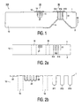
- Fig. 1 shows in a cross-sectional view a first embodiment of the electronic device 100 of the invention.
- the device 100 comprises a substrate 10 with a first side 1 and an opposed second side 2.
- a vertical trench capacitor 20 is present and exposed on the first side 1 in addition to a vertical interconnect 30.
- Both the vertical interconnect 30 and the capacitor 20 in this embodiment comprise a plurality of trenches, 21, 311, 312, 313.
- the vertical interconnect 30 comprises a first part 31 and a second part 32 of wider dimensions.
- the first part 31 is made by anisotropic etching from the first side 1
- the second part 32 is made by etching from the second side 2, and particularly wet-chemical etching.
- the device 100 comprises a couple of layers on its surfaces on the first and second sides 1,2 as well as in the trenches 21, 31, 32. Not shown here are first conductive surfaces 22 that constitute the bottom electrode of the vertical trench capacitor 20.
- a layer 11 of dielectric material is shown, that is present on nearly the whole surface.
- a layer 12 of electrically conductive material is present on top of the layer 11 of dielectric material.
- This layer is for instance polysilicon, but may alternatively be another material such as copper, sol-gel deposited silver, aluminum.
- the capacitor 20 and the interconnect 30 are provided with a further metallisation of AlCu in this case.
- the layers 12 and 13 can be used as interconnect layers and may be mutually separated at certain positions by an insulating layer.
- the second part 32 of the interconnect has its surface covered with a layer 14, in this case of electroplated copper.
- the copper extends on the second side 2 of the substrate and forms the wiring pattern.
- the layer 14 may fill the second part of the interconnect 30.
- Fig. 2 shows in cross-sectional view four stages in a first embodiment of the method. This first embodiment leads to a device 100 of the first embodiment, with minor variations.
- Fig 2a shows the first stage of the method, after etching from the first side has taken place.
- dry etching A mask was used with circular opening of 1.5 ⁇ m diameter and 3.5 ⁇ m spacing in the area of the capacitors, and openings of 10 ⁇ m diameter and 14 ⁇ m spacing in the area of the vertical interconnect.
- the mask contained a stack of 1 ⁇ m thermal oxide and 1.3 ⁇ m photoresist.
- the dry etching was executed at wafer level, using substrates of 150 mm diameter.
- the resistivity of the wafers was in the order of 1 to 5 m ⁇ cm, with the exception of high-ohmic zones 18,19 in the substrate, that had a resistivity of 1000-1500 ⁇ cm.
- the wafers were etched at room temperature in an ASE TM Inductively Coupled Plasma (ICP) reactor of STS. Typical etching conditions were 12 to 16 mTorr pressure and 20 °C chuck temperature, yielding etch rates of around 0.6 ⁇ m/min.
- ICP Inductively Coupled Plasma
- the macropore structures are characterized by a smooth pore wall with a rounded bottom and a pore depth uniformity of more than 97%.
- the trenches 21 with a mask opening of 1.5 ⁇ m diameter led to a depth of 40 ⁇ m and a diameter of 2 ⁇ m.
- the trenches 311,312,313 with a mask opening of 10 ⁇ m diameter led to a depth of 200 ⁇ m and a diameter of 12 ⁇ m.
- the pore depth is slightly larger than the mask opening due to underetch. Hence, the difference in openings in the mask led to differences in the pore depth, which phenomenon was exploited effectively in the invention.
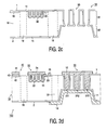
- Fig 2b shows a second stage in this first embodiment of the method.
- the etch mask was removed, and another mask was deposited.
- another mask was deposited.
- This mask for instance a nitride
- an implantation step was carried out.
- This implantation step provided a first conductive surface 22 in the trenches 21.
- the mask layout was such that also a conductive surface 42 was provided, to be used as bottom electrode of a planar capacitor.
- the high-ohmic zone 18 is present between the conductive surface 22 and 42, so as to prevent as much as possible any parasitic currents.
- a pad 23 was defmed in connection with the conductive surface 22, so as to enable electrical connection of the first conductive surface 22.
- Use was made of a P indiffusion from a pre-deposited phosphorous silicate glass layer. The silicate glass layer was then removed by wet etching in 1% (v/v) HF.
- Fig. 2c shows a third stage in this first embodiment of the method.
- the vertical interconnects 30 were opened from the second side 2 of the substrate 10 by wet-chemical etching. This led to the second parts 32 of the interconnects 30.
- Use was made herein of a KOH etch.
- Alternative methods for the interconnect opening include power blasting or lasering .
- a photolithographical mask was thereto provided on the second side of the substrate. It is observed that in the same step saw lanes can be defined on the second side 2 of the substrate 10. This will simplify the separation of the substrate into individual devices, such that other methods than sawing can be used.
- the dielectric layer 11 was in this example a nominally 30 nm 'ONO' dielectric layer stack consisting of a thermal oxide (5 nm), LPCVD nitride (20 nm) and an oxide layer (5 nm) deposited by LPCVD TEOS. The layer was deposited without a mask, such that the complete surface of the device was covered with the dielectric layer 11.
- the vertical interconnect 30 is not opened by wet-chemical etching from the second side, but by removal of part of the substrate. This can be done, by grinding and/or chemical-mechanical polishing.
- the grinding and/or polishing operation is particularly preferred in combination with the filling of the trenches 311-313 with a sacrificial layer, particularly a spin-on-glass material as known per se. This allows to finalize the thin-film structure on the first side 1 of the substrate 10 before opening the vertical interconnect 30, while at the same time the first side 1 constitutes a relatively planar surface.
- the spin-on-glass material can be removed in a gentle etching treatment, and both the first part 31 and the second part 32 of the interconnect 30 as far as present can be filled with electrically conductive material.
- Fig. 2d shows the device 100 after that in the following steps the dielectric layer 11 is partially etched away, and a layer of electrically conductive material is provided to define a top electrode 44 of the planar capacitor 40, the second conductive surface 24 of the vertical capacitor 20, the contact 25 to the first conductive surface 23, and the filling of the first part 31 of the vertical interconnect 30.
- a layer of electrically conductive material is provided to define a top electrode 44 of the planar capacitor 40, the second conductive surface 24 of the vertical capacitor 20, the contact 25 to the first conductive surface 23, and the filling of the first part 31 of the vertical interconnect 30.
- a 0.5 ⁇ m thick conductive layer of n-type in situ doped polysilicon It was deposited by LPCVD from SiH 4 and diluted PH 3 . After a furnace anneal step of 30 minutes at 1000 °C the conductivity of the polysilicon is in the order of 1 m ⁇ cm.
- the polysilicon is first deposited on the side-walls and then grows in the kinetic regime.
- the polysilicon layer 11 is also used as seed layer for the wiring pattern on the second side 2 of the substrate. This wiring pattern is grown by electroplating thereafter.
- the trenches 311, 312, 313 in the first part will be completely filled, even if the seed material is present only at their ends.
- dielectric material can be any single layer of oxide, nitride or the like; any material with a higher dielectric constant, such as tantalum oxide or hafnium oxide, or the like. These layers can be suitably applied with (low pressure) chemical vapor deposition. With this technique, the complete surface as far as uncovered by a mask is provided of the desired material.
- wet-chemical deposition techniques including sol-gel processing. It is preferred to apply an oxide layer, such as a thermal oxide, onto the substrate, in order to improve the adhesion.
- Another alternative is the use of a single nitride layer of about 15 nm - instead of the stack with 30 nm thickness. This increases the capacitance density from 30 to 90 nF/mm 2 , but reduces the breakdown voltage from 25 to 7 V.
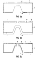
- Fig. 3 shows in cross-sectional view five stages in a second embodiment of the method of the invention.
- the first step of the method is herein the provision of the second parts 32 of the interconnects 30 from the second side of the substrate 10.
- This has the major advantage that after this first step no photolithographical step is needed anymore on the second side 2 of the substrate, until the provision of the wiring pattern 14 in the last step of the method.
- the trenches 21 of the vertical capacitor are not indicated in this Figure.
- Fig. 3a shows the obtained structure after providing the second parts 32 of the interconnect 30 from the second side 2 of the substrate 10.
- this was carried out by first providing a mask 51 of oxide and nitride on all sides of the substrates 10, then patterning the mask 51 according to the desired pattern on the second side 2 of the substrate 10 and finally wet-chemical etching of the silicon substrate 10 with KOH.
- Fig. 3b shows the result at a second stage of the method.
- the the mask 51 or at least the nitride layer thereof, is patterned from the first side 1 of the substrate 10, and used for definition of high ohmic substrate zones (not-shown).
- a hard mask 52 is deposited and patterned on the first side 1 of the substrate 10 to define the first part 31 of the interconnect 30.
- Fig. 3c shows the result at a third stage of the method.
- First the substrate 10 is etched from the first side 1 through the deposited mask. This etching can be done both with dry-etching and with wet-chemical etching. The etching is preferably carried out in the same step as the etching of trenches 21 to define a vertical capacitor. However, this is not essential.
- a conductive surface is provided in the manner described earlier with respect to the first embodiment of the method. Only hereafter the mask 51 is removed and the dielectric layer 11 is provided without a mask. Thereafter, a layer 12 of electrically conductive material, in this example polysilicon, is deposited and etched in accordance with any desired pattern.
- Fig. 3d shows the result at a fourth stage of the method.
- Contact windows have been etched in the dielectrical layer 11 on the first side 1 of the substrate 10.
- a patterned layer 13 of metal has been deposited, while leaving the area of the TEOS layer free.
- Fig. 3e shows the result at a fifth stage, after further steps.
- a patterned layer 16 of electrically insulating material After provision of a patterned layer 16 of electrically insulating material, a patterned layer 17 of electrically conductive material was provided.
- This second patterned layer 17, for instance of AlSiCu, has a sufficient thickness, for instance in the order of 1-4 microns, for definition of high-quality inductors.
- the pattern of electrically insulating material of the layers 15,16 functions as a mechanical support, such that the overlying area in the second metal layer 13 can be used as bond pad 28.
- the complete structure is then covered with a passivation layer 29, for instance of silicon nitride, that will be locally removed in the area of the bond pad 28.
- the substrate 10 is thereafter thinned by grinding from the second side 2 thereof. This is of course by no means a necessary step.
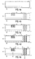
- Fig. 4 shows cross-sectional views of five stages in a third embodiment of the method of the invention.
- the first side 1 of the substrate 10 is provided with vertical capacitors 20, whereas a semiconductor device 50 is defined at the second side 2 of the substrate.
- Fig. 4a shows the first stage of the method. It starts with the semiconductor device 50, for instance an integrated circuit, having been fully processed.
- the substrate 10 is thereto an n-type substrate provided on its second side 2 with a p-type epitaxial layer, in which p-wells have been defined that act as channels for the individual transistors.
- An n + -connection is made from the second side 2 to the n-type substrate layer.
- This substrate layer has preferably a thickness of more than 40 ⁇ m and more preferably a thickness of at least more than 70 ⁇ m.
- the n-type layer provided with an n + -layer on its second side, so as to enable the effective etching of the vertical capacitors.
- the second side 2 of the substrate 10 is hereafter protected by a temporary carrier.
- it can be a two-layered stack of for instance a 1 micron thick oxide layer and a 1-10 micron thick photoresist layer. This stack can be present on all sides of the substrate 10, as is shown in Fig. 1a .
- This temporary carrier has the function to withstand pressure differences needed for dry etching, or to define the conditions for wet-chemical etching.
- the etching mask is furthermore applied to provide the desired implantation step, so as to create the first conductive surfaces of the vertical trench capacitors.
- Fig. 4b shows the result after the provision of the first and second trenches 21, 31. Due to the differences in pitch, the depth of the pores is controlled.
- Fig. 4c shows the result after removal of the etch mask and after provision of the dielectric layer 11.
- the removal of the etch mask effectively provides the opening of the second trenches 21 into vertical interconnects 30.
- the dielectric layer 11 is provided both in the first trenches 21 and in the second trenches 12, and is used as dielectric of the vertical capacitor 20 and as insulation of the vertical interconnect 20.
- no thermal oxide is used as part of the dielectric layer. Instead, an LPCVD oxide layer is applied. This LPCVD oxide is hereafter locally removed so as to open the bond pads of the integrated circuit 50.
- Fig 4d shows the result after the provision of the second electrically conductive surface 12, which is in this case a layer of TiN.
- This layer 12 is herein used as a seed layer.
- Alternative deposition techniques for seed layers such as sol-gel deposition of conductive oxides or sol-gel deposition of Ag.
- Fig. 4e shows the result after electroplating. Use is made of a mask, so as to define the desired wiring pattern. A further electrically conductive layer 13 is provided in the trenches 21,31. Thereafter, the parts of the seed layer under the mask are removed. The resulting device is very suitable for integration in a smartcard.
- Figs. 5 , 6 and 7 show in diagrammatical cross-sectional views three examples of the assembly according to the invention.
- Fig. 5 shows an assembly 300 including the device 100, a leadframe 310 and a semiconductor device 200.
- the assembly makes use of a double flip chip construction, in which the semiconductor device 200 is electrically connected to the leadframe 310 via the electronic device 100.
- the bumps 201 between devices 100 and 200 are herein for instance gold bumps, and the bumps 301 between leads 311 of the leadframe 310 and the device 100 are for instance solder bumps of SAC (tin-silver-copper alloy). Thermally, the semiconductor device 200 is coupled to the heatsink 312 of the leadframe 310 directly.
- the leadframe 210 comprises a first and a second electrically conductive layer of Cu.
- the lead frame 210 is formed by skillfully etching it with a semi-etching technique, first from the first side and then from the second side or the other way around.
- the heat sink 312 is customarily connected to the rest of the lead frame 310 by means of four wires.
- a conductive adhesive is applied i.e. a silver containing glass epoxy adhesive.
- Solder dots are provided on the leads 311, for example, by printing with a stencil.
- the solder is here a low-melting SAC solder which contains over 96% Sn, 3% Ag and about 0.5% Cu.
- the active device 200 together with the bumps 201 then has a thickness of 150 ⁇ 15 ⁇ m.
- the layers of the lead frame 310 have a thickness of 70 ⁇ 20 ⁇ m while in the location of the heat sink 312 relative to the device 100 there is a play of about 20 ⁇ m.
- the maximum spreading is thus about 55 ⁇ m.
- This spreading can be eliminated by remelting the solder balls and the solder dots, and slightly in the adhesive layer which, however, is chosen to be thin, for example of a thickness of about 20 ⁇ m.
- the heat sink 312 of the lead frame 310 is then pulled up when the adhesive layer shrinks. The result is a downward pressure.
- the resulting stress is relaxed by taking the bumps 201, 301 to beyond their reflow temperature. In this manner the bumps 201,301 are able to distort, and are particularly flattened.
- the second side 2 of the device 100 is here not provided with contact pads for coupling to an external carrier.
- the vertical interconnects 30 provide in this construction a thermal path to the second side 2 of the electronic device 100. This improves the heat-spreading function of the device 100.
- the vertical interconnects 30 are used for grounding. Although two vertical interconnects 30 provide an additional resistance to the ground, this construction of the grounding has the advantage that the ground can be assumed to have the same potential everywhere in the device. Such well defined ground is particularly preferred if the assembly 300 comprises more than a single element.
- the vertical capacitors (not-shown) are herein provided on the side 1 of the device 100 facing the semiconductor device 200.
- Fig. 6 shows an alternative embodiment of the assembly 300.
- This embodiment has practical advantages for multichip modules, in which more than one device 200 is assembled to the electronic device 100.
- This electronic device 100 acts here as the carrier of the assembly 300.
- the advantages are that devices 200 of different height can be included, and that there is no need for a simultaneous attachment of the devices 200 to an individual heatsinks 312 or one common heatsink 312.
- the assembly 300 of this embodiment is a chip-scale package without a leadframe, which can be provided at wafer level instead of at die level.
- a disadvantage of the embodiment is, however, the reduced possibilities for thermal dissipation.
- the heatsink 180 on the second side of the device 100 is provided with solder balls or other means for thermal coupling to an external carrier.
- Fig. 7 shows a further embodiment of the assembly 300. This embodiment is a more advanced version of the embodiment of Figure 6 . It has the further feature that devices 200 are attached to both the first side 1 and the second side 2 of the device 100. If desired, a leadframe with heatsink could be used as shown in Fig. 5 .
Landscapes
- Semiconductor Integrated Circuits (AREA)
- Internal Circuitry In Semiconductor Integrated Circuit Devices (AREA)
- Apparatuses And Processes For Manufacturing Resistors (AREA)
- Liquid Crystal (AREA)
- Electrophonic Musical Instruments (AREA)
- Engineering & Computer Science (AREA)
- Power Engineering (AREA)
- Physics & Mathematics (AREA)
- Geometry (AREA)
Claims (19)
- Elektronische Vorrichtung, die ein Halbleitersubstrat (10) mit einer ersten (1) und einer zweiten (2) Seite umfasst und mit einem Kondensator (20) und einer vertikalen Verbindung (30) durch das Substrat (10), die von der ersten (1) zur zweiten (2) Seite verläuft, versehen ist, wobei der Kondensator (20) auf der ersten Seite (1) vorhanden ist, dadurch gekennzeichnet, dass der Kondensator (20) ein vertikaler Grabenkondensator ist, der mit mehreren Gräben (21) versehen ist, in denen sich eine Schicht eines dielektrischen Materials (11) zwischen einer ersten (22) und einer zweiten (24) leitfähigen Oberfläche, die den Kondensator (20) bilden, befindet, wobei die Schicht des dielektrischen Materials (11) ferner als Isolation zwischen dem Substrat (10) und der vertikalen Verbindung (30) verwendet wird.
- Elektronische Vorrichtung nach Anspruch 1, wobei die vertikale Verbindung (30) ein erstes Teilstück (31) und ein zweites Teilstück (32) aufweist, und wobei das erste Teilstück (31) auf der ersten Seite (1) des Substrats (10) freiliegt, schmaler ist als das zweite Teilstück (32), und eine im Wesentlichen zylindrische Form aufweist.
- Elektronische Vorrichtung nach Anspruch 1, dadurch gekennzeichnet, dass Gräben (311, 312, 313) der vertikalen Verbindung (30) im Wesentlichen mit elektrisch leitfähigem Material (12) gefüllt sind.
- Elektronische Vorrichtung nach Anspruch 2, dadurch gekennzeichnet, dass die vertikale Verbindung (30) mehrere parallele Durchgangslöcher (311, 312, 313) durch das Substrat (10) umfasst, von denen jedes mit elektrisch leitfähigem Material (12) gefüllt ist.
- Elektronische Vorrichtung nach Anspruch 1, dadurch gekennzeichnet, dass:Kontaktfelder für die Verbindung mit einem externen Träger auf der zweiten Seite vorhanden sind;eine erste vertikale Verbindung zur Erdung verwendet wird, und eine zweite vertikale Verbindung zur Signalübertragung verwendet wird.
- Elektronische Vorrichtung nach Anspruch 5, dadurch gekennzeichnet, dass die erste und die zweite vertikale Verbindung so ausgeführt sind, dass sie eine koaxiale Anordnung bilden.
- Elektronische Vorrichtung nach Anspruch 1, dadurch gekennzeichnet, dass eine integrierte Schaltung auf der zweiten Seite (2) des Substrats (10) definiert ist.
- Elektronische Vorrichtung nach Anspruch 1, dadurch gekennzeichnet, dass das Substrat (10) eine hochohmige Zone (18, 19) umfasst, die benachbart zum vertikalen Kondensator (20) vorhanden ist und als Schutz gegen parasitäre Ströme dient.
- Elektronische Vorrichtung nach Anspruch 1, dadurch gekennzeichnet, dass ein Planarkondensator (40) auf der ersten Seite (1) des Substrats (10) vorhanden ist, wobei der Planarkondensator (40) die gleiche Schicht des dielektrischen Materials (11) umfasst wie der vertikale Kondensator (20).
- Anordnung, die die elektronische Vorrichtung nach irgendeinem der vorangehenden Ansprüche, sowie eine Halbleitervorrichtung umfasst, wobei die Halbleitervorrichtung mit Verbindungsfeldern elektrisch verbunden ist, die auf der ersten Seite (1) des Substrats (10) vorhanden sind.
- Verfahren der Herstellung einer elektronischen Vorrichtung, die ein Halbleitersubstrat (10) mit einer ersten (1) und einer zweiten (2) Seite umfasst und mit einem Kondensator (20) und einer vertikalen Verbindung (30), die sich von der ersten (1) zur zweiten (2) Seite erstreckt, versehen ist, wobei sich der Kondensator (20) auf der ersten Seite (1) befindet, und wobei das Verfahren die Schritte umfasst:Bereitstellen erster Gräben (21) im Substrat (10), einschließlich des Schritts des Ätzens von der ersten Seite (1) des Substrats (10);Bereitstellen zweiter Gräben (311, 312, 313) im Substrat durch Ätzen von einer Seite des Substrats (10), und Öffnen der zweiten Gräben durch Entfernen von Material von der gegenüberliegenden Seite des Substrats (10);Versehen der ersten Gräben (21) mit einer leitfähigen Oberfläche (22);Aufbringen einer Schicht eines dielektrischen Materials (11) auf das Substrat (10), die wenigstens die erste Seite (1) des Substrats (10) und die Innenflächen der ersten (21) und der zweiten (311, 312, 313) Gräben bedeckt; undAufbringen eines elektrisch leitfähigen Materials (24, 12) in den ersten Gräben (21) und in den zweiten Gräben (311, 312, 313), wobei das leitfähige Material (24) der ersten Gräben (21) gemeinsam mit der Schicht des dielektrischen Materials (11) und der leitfähigen Oberfläche (22) den Kondensator (20) bildet, und wobei das leitfähige Material (12) der zweiten Gräben (311, 312, 313) die vertikalen Verbindungen (30) bildet.
- Verfahren nach Anspruch 11, wobei die ersten Gräben (21) und die zweiten Gräben (311, 312, 313) in einem einzigen Schritt geätzt werden, und wobei die ersten Gräben (21) einen kleineren Durchmesser aufweisen als die zweiten Gräben (311, 312, 313), die zu den Durchgangslöchern führen, mit dem Ergebnis, dass die zweiten Gräben (311, 312, 313) sich weiter in das Substrat (10) erstrecken als die ersten Gräben (21), und wobei die Gräben (21) Innenflächen aufweisen.
- Verfahren nach Anspruch 12, dadurch gekennzeichnet, dass der Schritt des Aufbringens von leitfähigem Material (12) in den zweiten Gräben (311, 312, 313) die Schritte des Aufbringens einer Keimschicht und des Galvanisierens umfasst.
- Verfahren nach Anspruch 12, dadurch gekennzeichnet, dass mehrere zweite Gräben (311, 312, 313) benachbart und wechselseitig verbunden sind, um somit eine einzelne vertikale Verbindung (30) zu bilden.
- Verfahren nach Anspruch 14, wobei das elektrisch leitfähige Material (24, 12), das in den ersten (21) und den zweiten (311, 312, 313) Gräben aufgebracht wird, Polysilicium ist.
- Verfahren nach Anspruch 11, wobei der Schritt des Beseitigens von Material zum Öffnen der zweiten Gräben (311, 312, 313) den Schritt des chemischen Nassätzens umfasst, um einen Hohlraum zu bilden, wobei der Hohlraum einen größeren Durchmesser aufweist als die zweiten Gräben (311, 312, 313).
- Verfahren nach Anspruch 11, wobei die zweiten Gräben (311, 312, 313) durch chemisches Nassätzen von der zweiten Seite (2) des Substrats (10) vor der Bereitstellung der ersten Gräben (21) gebildet werden, und wobei die zweiten Gräben (311, 312, 313) als Hohlräume ausgeformt sind und einen größeren Durchmesser aufweisen als die ersten Gräben (21).
- Verfahren nach Anspruch 17, wobei die zweiten Gräben (311, 312, 313) durch Ätzen im gleichen Schritt wie das Ätzen der ersten Gräben (21) geöffnet werden.
- Verfahren nach Anspruch 17, wobei die zweiten Gräben (311, 312, 313) sich bis zur ersten Seite (1) des Halbleitersubstrats (10) erstrecken und durch eine Ätzstoppschicht bedeckt sind, die auf der ersten Seite (1) des Substrats (10) vorgesehen ist.
Priority Applications (1)
| Application Number | Priority Date | Filing Date | Title |
|---|---|---|---|
| EP04736684A EP1639634B1 (de) | 2003-06-20 | 2004-06-11 | Elektronische vorrichtung, anordnung und verfahren zum herstellen einer elektronischen vorrichtung |
Applications Claiming Priority (4)
| Application Number | Priority Date | Filing Date | Title |
|---|---|---|---|
| EP03300035 | 2003-06-20 | ||
| EP04300132 | 2004-03-10 | ||
| PCT/IB2004/050887 WO2004114397A1 (en) | 2003-06-20 | 2004-06-11 | Electronic device, assembly and methods of manufacturing an electronic device |
| EP04736684A EP1639634B1 (de) | 2003-06-20 | 2004-06-11 | Elektronische vorrichtung, anordnung und verfahren zum herstellen einer elektronischen vorrichtung |
Publications (2)
| Publication Number | Publication Date |
|---|---|
| EP1639634A1 EP1639634A1 (de) | 2006-03-29 |
| EP1639634B1 true EP1639634B1 (de) | 2009-04-01 |
Family
ID=33542572
Family Applications (1)
| Application Number | Title | Priority Date | Filing Date |
|---|---|---|---|
| EP04736684A Expired - Lifetime EP1639634B1 (de) | 2003-06-20 | 2004-06-11 | Elektronische vorrichtung, anordnung und verfahren zum herstellen einer elektronischen vorrichtung |
Country Status (7)
| Country | Link |
|---|---|
| US (2) | US9530857B2 (de) |
| EP (1) | EP1639634B1 (de) |
| JP (1) | JP5058597B2 (de) |
| KR (1) | KR101086520B1 (de) |
| AT (1) | ATE427560T1 (de) |
| DE (1) | DE602004020344D1 (de) |
| WO (1) | WO2004114397A1 (de) |
Cited By (1)
| Publication number | Priority date | Publication date | Assignee | Title |
|---|---|---|---|---|
| TWI890725B (zh) * | 2020-01-09 | 2025-07-21 | 日商村田製作所股份有限公司 | 具有配備有由基底所支撐的電容器的差動傳輸線的電子裝置以及相應的製造方法 |
Families Citing this family (80)
| Publication number | Priority date | Publication date | Assignee | Title |
|---|---|---|---|---|
| WO2005088699A1 (en) * | 2004-03-10 | 2005-09-22 | Koninklijke Philips Electronics N.V. | Method of manufacturing an electronic device and a resulting device |
| CN101356637B (zh) * | 2005-11-08 | 2012-06-06 | Nxp股份有限公司 | 使用临时帽层产生受到覆盖的穿透衬底的通道 |
| US8085524B2 (en) | 2005-11-08 | 2011-12-27 | Ipdia | Integrated capacitor arrangement for ultrahigh capacitance values |
| US7844997B2 (en) * | 2006-01-12 | 2010-11-30 | Honeywell International Inc. | Securing standard test access port with an independent security key interface |
| US7626257B2 (en) * | 2006-01-18 | 2009-12-01 | Infineon Technologies Ag | Semiconductor devices and methods of manufacture thereof |
| US8171542B2 (en) * | 2006-02-13 | 2012-05-01 | Honeywell International Inc. | Advanced encryption standard to provide hardware key interface |
| US8135959B2 (en) * | 2006-04-07 | 2012-03-13 | Honeywell International Inc. | External key to provide protection to devices |
| TWI451561B (zh) | 2006-05-02 | 2014-09-01 | Nxp Bv | 包括經改進電極之電子裝置 |
| US8502362B2 (en) * | 2011-08-16 | 2013-08-06 | Advanced Analogic Technologies, Incorporated | Semiconductor package containing silicon-on-insulator die mounted in bump-on-leadframe manner to provide low thermal resistance |
| WO2007131967A1 (en) * | 2006-05-15 | 2007-11-22 | Koninklijke Philips Electronics N.V. | Integrated low-loss capacitor-arrray structure |
| US7944658B2 (en) * | 2006-06-20 | 2011-05-17 | Nxp B.V. | Integrated circuit and assembly therewith |
| TW200818534A (en) * | 2006-08-10 | 2008-04-16 | Icemos Technology Corp | Method of manufacturing a photodiode array with through-wafer vias |
| US7531445B2 (en) | 2006-09-26 | 2009-05-12 | Hymite A/S | Formation of through-wafer electrical interconnections and other structures using a thin dielectric membrane |
| US8513789B2 (en) | 2006-10-10 | 2013-08-20 | Tessera, Inc. | Edge connect wafer level stacking with leads extending along edges |
| US7901989B2 (en) | 2006-10-10 | 2011-03-08 | Tessera, Inc. | Reconstituted wafer level stacking |
| US7829438B2 (en) | 2006-10-10 | 2010-11-09 | Tessera, Inc. | Edge connect wafer level stacking |
| US8569876B2 (en) | 2006-11-22 | 2013-10-29 | Tessera, Inc. | Packaged semiconductor chips with array |
| US7791199B2 (en) | 2006-11-22 | 2010-09-07 | Tessera, Inc. | Packaged semiconductor chips |
| US7952195B2 (en) | 2006-12-28 | 2011-05-31 | Tessera, Inc. | Stacked packages with bridging traces |
| DE102007009383A1 (de) * | 2007-02-20 | 2008-08-21 | Fraunhofer-Gesellschaft zur Förderung der angewandten Forschung e.V. | Halbleiteranordnung und Verfahren zu deren Herstellung |
| JP5584474B2 (ja) | 2007-03-05 | 2014-09-03 | インヴェンサス・コーポレイション | 貫通ビアによって前面接点に接続された後面接点を有するチップ |
| KR20100015378A (ko) * | 2007-03-23 | 2010-02-12 | 이노배티어, 인코프레이티드 | 스텝 카드 및 스텝 카드를 제조하는 방법 |
| DE102007019552B4 (de) * | 2007-04-25 | 2009-12-17 | Infineon Technologies Ag | Verfahren zur Herstellung eines Substrats mit Durchführung sowie Substrat und Halbleitermodul mit Durchführung |
| CN101682252B (zh) | 2007-05-10 | 2013-10-23 | Nxp股份有限公司 | 包含可重构电容器单元的直流-直流变换器 |
| US8729665B2 (en) | 2007-05-10 | 2014-05-20 | Ipdia | Integration substrate with a ultra-high-density capacitor and a through-substrate via |
| DE102007026445A1 (de) * | 2007-06-06 | 2008-12-11 | Robert Bosch Gmbh | Mikromechanisches Bauelement und Verfahren zur Herstellung eines mikromechanischen Bauelements |
| CN101785103B (zh) | 2007-07-05 | 2011-12-28 | Aac微技术有限公司 | 低阻抗晶圆穿孔 |
| KR101458538B1 (ko) | 2007-07-27 | 2014-11-07 | 테세라, 인코포레이티드 | 적층형 마이크로 전자 유닛, 및 이의 제조방법 |
| CN103178032B (zh) | 2007-07-31 | 2017-06-20 | 英闻萨斯有限公司 | 使用穿透硅通道的半导体封装方法 |
| US8551815B2 (en) | 2007-08-03 | 2013-10-08 | Tessera, Inc. | Stack packages using reconstituted wafers |
| US8043895B2 (en) | 2007-08-09 | 2011-10-25 | Tessera, Inc. | Method of fabricating stacked assembly including plurality of stacked microelectronic elements |
| JP4585561B2 (ja) * | 2007-09-04 | 2010-11-24 | 株式会社東芝 | 半導体装置の製造方法 |
| CN101946304B (zh) | 2008-02-20 | 2013-06-05 | Nxp股份有限公司 | 包括在衬底的两个面上形成的平面形状电容器的超高密度容量 |
| CN102067310B (zh) | 2008-06-16 | 2013-08-21 | 泰塞拉公司 | 带有边缘触头的晶片级芯片规模封装的堆叠及其制造方法 |
| CN102164845A (zh) * | 2008-09-30 | 2011-08-24 | Nxp股份有限公司 | 鲁棒高宽比半导体器件 |
| US7943473B2 (en) * | 2009-01-13 | 2011-05-17 | Maxim Integrated Products, Inc. | Minimum cost method for forming high density passive capacitors for replacement of discrete board capacitors using a minimum cost 3D wafer-to-wafer modular integration scheme |
| CN102422412A (zh) | 2009-03-13 | 2012-04-18 | 德塞拉股份有限公司 | 具有穿过结合垫延伸的通路的堆叠式微电子组件 |
| US8062975B2 (en) * | 2009-04-16 | 2011-11-22 | Freescale Semiconductor, Inc. | Through substrate vias |
| US9640437B2 (en) | 2010-07-23 | 2017-05-02 | Tessera, Inc. | Methods of forming semiconductor elements using micro-abrasive particle stream |
| US8796135B2 (en) | 2010-07-23 | 2014-08-05 | Tessera, Inc. | Microelectronic elements with rear contacts connected with via first or via middle structures |
| US8791575B2 (en) | 2010-07-23 | 2014-07-29 | Tessera, Inc. | Microelectronic elements having metallic pads overlying vias |
| US8076184B1 (en) * | 2010-08-16 | 2011-12-13 | Stats Chippac, Ltd. | Semiconductor device and method of forming wafer-level multi-row etched leadframe with base leads and embedded semiconductor die |
| US8610259B2 (en) | 2010-09-17 | 2013-12-17 | Tessera, Inc. | Multi-function and shielded 3D interconnects |
| US8847380B2 (en) | 2010-09-17 | 2014-09-30 | Tessera, Inc. | Staged via formation from both sides of chip |
| JP5141740B2 (ja) * | 2010-10-04 | 2013-02-13 | 株式会社デンソー | 半導体装置およびその製造方法 |
| US8232173B2 (en) * | 2010-11-01 | 2012-07-31 | International Business Machines Corporation | Structure and design structure for high-Q value inductor and method of manufacturing the same |
| EP2450995A1 (de) | 2010-11-03 | 2012-05-09 | Nxp B.V. | Batterie |
| KR101059490B1 (ko) | 2010-11-15 | 2011-08-25 | 테세라 리써치 엘엘씨 | 임베드된 트레이스에 의해 구성된 전도성 패드 |
| US8587126B2 (en) | 2010-12-02 | 2013-11-19 | Tessera, Inc. | Stacked microelectronic assembly with TSVs formed in stages with plural active chips |
| US8637968B2 (en) | 2010-12-02 | 2014-01-28 | Tessera, Inc. | Stacked microelectronic assembly having interposer connecting active chips |
| US8736066B2 (en) * | 2010-12-02 | 2014-05-27 | Tessera, Inc. | Stacked microelectronic assemby with TSVS formed in stages and carrier above chip |
| US8610264B2 (en) | 2010-12-08 | 2013-12-17 | Tessera, Inc. | Compliant interconnects in wafers |
| US8502340B2 (en) * | 2010-12-09 | 2013-08-06 | Tessera, Inc. | High density three-dimensional integrated capacitors |
| US8742541B2 (en) | 2010-12-09 | 2014-06-03 | Tessera, Inc. | High density three-dimensional integrated capacitors |
| JP6028887B2 (ja) * | 2011-06-13 | 2016-11-24 | セイコーエプソン株式会社 | 配線基板、赤外線センサー及び貫通電極形成方法 |
| JP5834563B2 (ja) * | 2011-07-14 | 2015-12-24 | セイコーエプソン株式会社 | 半導体装置の製造方法 |
| US20140021603A1 (en) * | 2012-07-23 | 2014-01-23 | Rf Micro Devices, Inc. | Using an interconnect bump to traverse through a passivation layer of a semiconductor die |
| KR101985404B1 (ko) * | 2012-09-13 | 2019-06-03 | 해성디에스 주식회사 | 회로 기판의 제조 방법 및 그 방법으로 제조된 회로 기판 |
| US10283854B2 (en) | 2012-10-08 | 2019-05-07 | Taoglas Group Holdings Limited | Low-cost ultra wideband LTE antenna |
| CN105097794A (zh) * | 2014-04-25 | 2015-11-25 | 中芯国际集成电路制造(上海)有限公司 | Esd防护器件及其制作方法 |
| JP6528550B2 (ja) * | 2015-06-11 | 2019-06-12 | 株式会社デンソー | 半導体装置およびその製造方法 |
| US9893058B2 (en) | 2015-09-17 | 2018-02-13 | Semiconductor Components Industries, Llc | Method of manufacturing a semiconductor device having reduced on-state resistance and structure |
| US11342189B2 (en) | 2015-09-17 | 2022-05-24 | Semiconductor Components Industries, Llc | Semiconductor packages with die including cavities and related methods |
| US9755310B2 (en) | 2015-11-20 | 2017-09-05 | Taoglas Limited | Ten-frequency band antenna |
| CN105371878B (zh) | 2015-12-04 | 2017-08-25 | 歌尔股份有限公司 | 一种环境传感器及其制造方法 |
| RU2725617C2 (ru) * | 2016-03-01 | 2020-07-03 | Кардлаб Апс | Схемный слой для карты с интегральной схемой |
| US10432172B2 (en) * | 2016-09-01 | 2019-10-01 | Samsung Electro-Mechanics Co., Ltd. | Bulk acoustic filter device and method of manufacturing the same |
| US10944379B2 (en) * | 2016-12-14 | 2021-03-09 | Qualcomm Incorporated | Hybrid passive-on-glass (POG) acoustic filter |
| US10199372B2 (en) * | 2017-06-23 | 2019-02-05 | Infineon Technologies Ag | Monolithically integrated chip including active electrical components and passive electrical components with chip edge stabilization structures |
| US10381161B2 (en) * | 2017-11-06 | 2019-08-13 | Advanced Semiconductor Engineering, Inc. | Capacitor structure |
| JP7021021B2 (ja) * | 2018-07-25 | 2022-02-16 | 日産自動車株式会社 | 半導体装置及びその製造方法 |
| MY201172A (en) * | 2018-09-19 | 2024-02-08 | Intel Corp | Stacked through-silicon vias for multi-device packages |
| US11404534B2 (en) | 2019-06-28 | 2022-08-02 | Taiwan Semiconductor Manufacturing Company, Ltd. | Backside capacitor techniques |
| EP3930008A1 (de) | 2020-06-24 | 2021-12-29 | Murata Manufacturing Co., Ltd. | Elektronisches bauelement mit einer kapazitiven 3d-struktur |
| JP2022147628A (ja) | 2021-03-23 | 2022-10-06 | 株式会社東芝 | 半導体装置 |
| US20230018448A1 (en) * | 2021-07-14 | 2023-01-19 | Qualcomm Incorporated | Reduced impedance substrate |
| US20230394217A1 (en) * | 2022-06-07 | 2023-12-07 | Taiwan Semiconductor Manufacturing Co., Ltd. | Integrated circuit (ic) design methods using process friendly cell architectures |
| FR3149467A1 (fr) * | 2023-05-30 | 2024-12-06 | Psa Automobiles Sa | Dispositif semiconducteur comportant un condensateur de decouplage a structure stratifiee |
| WO2025154391A1 (ja) * | 2024-01-17 | 2025-07-24 | パナソニックIpマネジメント株式会社 | インタポーザ |
| CN119786435A (zh) * | 2024-12-19 | 2025-04-08 | 深圳大学 | 一种双层镀铜的深槽电容兼容硅芯同轴硅通孔方法 |
Family Cites Families (22)
| Publication number | Priority date | Publication date | Assignee | Title |
|---|---|---|---|---|
| DE1514818A1 (de) * | 1951-01-28 | 1969-05-08 | Telefunken Patent | Festkoerperschaltung,bestehend aus einem Halbleiterkoerper mit eingebrachten aktiven Bauelementen und einer Isolierschicht mit aufgebrachten passiven Bauelementen und Leitungsbahnen |
| US4017885A (en) * | 1973-10-25 | 1977-04-12 | Texas Instruments Incorporated | Large value capacitor |
| EP0516031A1 (de) * | 1991-05-29 | 1992-12-02 | Ramtron International Corporation | Ferroelektrische Stapelspeicherzelle und Herstellungsverfahren |
| JPH07135210A (ja) * | 1993-11-10 | 1995-05-23 | Mitsubishi Electric Corp | 半導体装置及びその製造方法 |
| US5872393A (en) * | 1995-10-30 | 1999-02-16 | Matsushita Electric Industrial Co., Ltd. | RF semiconductor device and a method for manufacturing the same |
| US5905279A (en) * | 1996-04-09 | 1999-05-18 | Kabushiki Kaisha Toshiba | Low resistant trench fill for a semiconductor device |
| JP3724110B2 (ja) * | 1997-04-24 | 2005-12-07 | 三菱電機株式会社 | 半導体装置の製造方法 |
| US5998292A (en) * | 1997-11-12 | 1999-12-07 | International Business Machines Corporation | Method for making three dimensional circuit integration |
| US6025226A (en) * | 1998-01-15 | 2000-02-15 | International Business Machines Corporation | Method of forming a capacitor and a capacitor formed using the method |
| TW442873B (en) | 1999-01-14 | 2001-06-23 | United Microelectronics Corp | Three-dimension stack-type chip structure and its manufacturing method |
| US6221769B1 (en) * | 1999-03-05 | 2001-04-24 | International Business Machines Corporation | Method for integrated circuit power and electrical connections via through-wafer interconnects |
| US6617681B1 (en) | 1999-06-28 | 2003-09-09 | Intel Corporation | Interposer and method of making same |
| US6559499B1 (en) * | 2000-01-04 | 2003-05-06 | Agere Systems Inc. | Process for fabricating an integrated circuit device having capacitors with a multilevel metallization |
| US6384468B1 (en) | 2000-02-07 | 2002-05-07 | International Business Machines Corporation | Capacitor and method for forming same |
| JP4386525B2 (ja) * | 2000-02-23 | 2009-12-16 | イビデン株式会社 | プリント配線板 |
| JP3796099B2 (ja) | 2000-05-12 | 2006-07-12 | 新光電気工業株式会社 | 半導体装置用インターポーザー、その製造方法および半導体装置 |
| JP4895420B2 (ja) | 2000-08-10 | 2012-03-14 | ルネサスエレクトロニクス株式会社 | 半導体装置およびその製造方法 |
| US6538300B1 (en) * | 2000-09-14 | 2003-03-25 | Vishay Intertechnology, Inc. | Precision high-frequency capacitor formed on semiconductor substrate |
| US6737740B2 (en) * | 2001-02-08 | 2004-05-18 | Micron Technology, Inc. | High performance silicon contact for flip chip |
| US6420776B1 (en) * | 2001-03-01 | 2002-07-16 | Amkor Technology, Inc. | Structure including electronic components singulated using laser cutting |
| FR2830683A1 (fr) * | 2001-10-10 | 2003-04-11 | St Microelectronics Sa | Realisation d'inductance et de via dans un circuit monolithique |
| US7030481B2 (en) | 2002-12-09 | 2006-04-18 | Internation Business Machines Corporation | High density chip carrier with integrated passive devices |
-
2004
- 2004-06-11 EP EP04736684A patent/EP1639634B1/de not_active Expired - Lifetime
- 2004-06-11 DE DE602004020344T patent/DE602004020344D1/de not_active Expired - Lifetime
- 2004-06-11 JP JP2006516678A patent/JP5058597B2/ja not_active Expired - Lifetime
- 2004-06-11 US US10/560,717 patent/US9530857B2/en active Active
- 2004-06-11 AT AT04736684T patent/ATE427560T1/de not_active IP Right Cessation
- 2004-06-11 WO PCT/IB2004/050887 patent/WO2004114397A1/en not_active Ceased
- 2004-06-11 KR KR1020057024459A patent/KR101086520B1/ko not_active Expired - Fee Related
-
2016
- 2016-12-21 US US15/387,035 patent/US20170170131A1/en not_active Abandoned
Cited By (2)
| Publication number | Priority date | Publication date | Assignee | Title |
|---|---|---|---|---|
| TWI890725B (zh) * | 2020-01-09 | 2025-07-21 | 日商村田製作所股份有限公司 | 具有配備有由基底所支撐的電容器的差動傳輸線的電子裝置以及相應的製造方法 |
| EP3849286B1 (de) * | 2020-01-09 | 2025-08-27 | Murata Manufacturing Co., Ltd. | Elektronische vorrichtung mit differentiellen übertragungsleitungen, die mit von einer basis getragenen 3d-kondensatoren ausgestattet sind, und entsprechendes herstellungsverfahren |
Also Published As
| Publication number | Publication date |
|---|---|
| DE602004020344D1 (de) | 2009-05-14 |
| KR101086520B1 (ko) | 2011-11-23 |
| JP5058597B2 (ja) | 2012-10-24 |
| WO2004114397A1 (en) | 2004-12-29 |
| KR20060033866A (ko) | 2006-04-20 |
| US20060131691A1 (en) | 2006-06-22 |
| JP2007516589A (ja) | 2007-06-21 |
| US20170170131A1 (en) | 2017-06-15 |
| ATE427560T1 (de) | 2009-04-15 |
| EP1639634A1 (de) | 2006-03-29 |
| US9530857B2 (en) | 2016-12-27 |
Similar Documents
| Publication | Publication Date | Title |
|---|---|---|
| EP1639634B1 (de) | Elektronische vorrichtung, anordnung und verfahren zum herstellen einer elektronischen vorrichtung | |
| US7220667B2 (en) | Semiconductor device and method of fabricating the same | |
| CN100365798C (zh) | 电子器件、组件及制造电子器件的方法 | |
| US5753529A (en) | Surface mount and flip chip technology for total integrated circuit isolation | |
| JP5285829B2 (ja) | インターポーザおよびその製造方法 | |
| US6873038B2 (en) | Capacitor and semiconductor device and method for fabricating the semiconductor device | |
| US6300250B1 (en) | Method of forming bumps for flip chip applications | |
| JP4979213B2 (ja) | 回路基板、回路基板の製造方法および回路装置 | |
| US11735497B2 (en) | Integrated passive device and fabrication method using a last through-substrate via | |
| US20130026632A1 (en) | Semiconductor element-embedded wiring substrate | |
| JP2009500820A (ja) | アセンブリを製造する方法及びアセンブリ | |
| KR20110050957A (ko) | 반도체 소자의 관통 비아 콘택 및 그 형성 방법 | |
| US10014240B1 (en) | Embedded component package and fabrication method | |
| US20020085336A1 (en) | High performance via capacitor and method for manufacturing same | |
| US6908845B2 (en) | Integrated circuit die and an electronic assembly having a three-dimensional interconnection scheme | |
| WO2016137892A1 (en) | Microelectronic assemblies formed using metal silicide, and methods of fabrication | |
| JP2008522402A (ja) | 選択的陽極酸化された金属を用いたパッケージ及びその製作方法 | |
| JP4678720B2 (ja) | 回路基板およびその製造方法、半導体装置およびその製造方法 | |
| WO2005088699A1 (en) | Method of manufacturing an electronic device and a resulting device | |
| JP4323137B2 (ja) | 基板埋め込み用キャパシタ、基板埋め込み用キャパシタを埋め込んだ回路基板及び基板埋め込み用キャパシタの製造方法 | |
| US20030183943A1 (en) | Integrated circuit die and an electronic assembly having a three-dimensional interconnection scheme | |
| US20080142964A1 (en) | Tubular-shaped bumps for integrated circuit devices and methods of fabrication | |
| CN1957465B (zh) | 半导体器件及配线基板 | |
| CN216528949U (zh) | 一种基于热氧化法制作的集成无源器件 | |
| CN114464584B (zh) | 具有瓶形硅穿孔的半导体元件结构及其制备方法 |
Legal Events
| Date | Code | Title | Description |
|---|---|---|---|
| PUAI | Public reference made under article 153(3) epc to a published international application that has entered the european phase |
Free format text: ORIGINAL CODE: 0009012 |
|
| 17P | Request for examination filed |
Effective date: 20060120 |
|
| AK | Designated contracting states |
Kind code of ref document: A1 Designated state(s): AT BE BG CH CY CZ DE DK EE ES FI FR GB GR HU IE IT LI LU MC NL PL PT RO SE SI SK TR |
|
| DAX | Request for extension of the european patent (deleted) | ||
| RAP1 | Party data changed (applicant data changed or rights of an application transferred) |
Owner name: NXP B.V. |
|
| GRAP | Despatch of communication of intention to grant a patent |
Free format text: ORIGINAL CODE: EPIDOSNIGR1 |
|
| RIC1 | Information provided on ipc code assigned before grant |
Ipc: H01L 23/48 20060101ALI20080908BHEP Ipc: H01L 21/8242 20060101ALI20080908BHEP Ipc: H01L 27/06 20060101ALI20080908BHEP Ipc: H01L 21/334 20060101ALI20080908BHEP Ipc: H01L 21/768 20060101AFI20080908BHEP |
|
| GRAS | Grant fee paid |
Free format text: ORIGINAL CODE: EPIDOSNIGR3 |
|
| GRAA | (expected) grant |
Free format text: ORIGINAL CODE: 0009210 |
|
| AK | Designated contracting states |
Kind code of ref document: B1 Designated state(s): AT BE BG CH CY CZ DE DK EE ES FI FR GB GR HU IE IT LI LU MC NL PL PT RO SE SI SK TR |
|
| REG | Reference to a national code |
Ref country code: GB Ref legal event code: FG4D |
|
| REG | Reference to a national code |
Ref country code: CH Ref legal event code: EP |
|
| REG | Reference to a national code |
Ref country code: IE Ref legal event code: FG4D |
|
| REF | Corresponds to: |
Ref document number: 602004020344 Country of ref document: DE Date of ref document: 20090514 Kind code of ref document: P |
|
| PG25 | Lapsed in a contracting state [announced via postgrant information from national office to epo] |
Ref country code: SI Free format text: LAPSE BECAUSE OF FAILURE TO SUBMIT A TRANSLATION OF THE DESCRIPTION OR TO PAY THE FEE WITHIN THE PRESCRIBED TIME-LIMIT Effective date: 20090401 |
|
| NLV1 | Nl: lapsed or annulled due to failure to fulfill the requirements of art. 29p and 29m of the patents act | ||
| PG25 | Lapsed in a contracting state [announced via postgrant information from national office to epo] |
Ref country code: EE Free format text: LAPSE BECAUSE OF FAILURE TO SUBMIT A TRANSLATION OF THE DESCRIPTION OR TO PAY THE FEE WITHIN THE PRESCRIBED TIME-LIMIT Effective date: 20090401 Ref country code: PT Free format text: LAPSE BECAUSE OF FAILURE TO SUBMIT A TRANSLATION OF THE DESCRIPTION OR TO PAY THE FEE WITHIN THE PRESCRIBED TIME-LIMIT Effective date: 20090902 Ref country code: ES Free format text: LAPSE BECAUSE OF FAILURE TO SUBMIT A TRANSLATION OF THE DESCRIPTION OR TO PAY THE FEE WITHIN THE PRESCRIBED TIME-LIMIT Effective date: 20090712 Ref country code: AT Free format text: LAPSE BECAUSE OF FAILURE TO SUBMIT A TRANSLATION OF THE DESCRIPTION OR TO PAY THE FEE WITHIN THE PRESCRIBED TIME-LIMIT Effective date: 20090401 Ref country code: FI Free format text: LAPSE BECAUSE OF FAILURE TO SUBMIT A TRANSLATION OF THE DESCRIPTION OR TO PAY THE FEE WITHIN THE PRESCRIBED TIME-LIMIT Effective date: 20090401 |
|
| PG25 | Lapsed in a contracting state [announced via postgrant information from national office to epo] |
Ref country code: SE Free format text: LAPSE BECAUSE OF FAILURE TO SUBMIT A TRANSLATION OF THE DESCRIPTION OR TO PAY THE FEE WITHIN THE PRESCRIBED TIME-LIMIT Effective date: 20090701 Ref country code: NL Free format text: LAPSE BECAUSE OF FAILURE TO SUBMIT A TRANSLATION OF THE DESCRIPTION OR TO PAY THE FEE WITHIN THE PRESCRIBED TIME-LIMIT Effective date: 20090401 Ref country code: PL Free format text: LAPSE BECAUSE OF FAILURE TO SUBMIT A TRANSLATION OF THE DESCRIPTION OR TO PAY THE FEE WITHIN THE PRESCRIBED TIME-LIMIT Effective date: 20090401 |
|
| PG25 | Lapsed in a contracting state [announced via postgrant information from national office to epo] |
Ref country code: CZ Free format text: LAPSE BECAUSE OF FAILURE TO SUBMIT A TRANSLATION OF THE DESCRIPTION OR TO PAY THE FEE WITHIN THE PRESCRIBED TIME-LIMIT Effective date: 20090401 Ref country code: RO Free format text: LAPSE BECAUSE OF FAILURE TO SUBMIT A TRANSLATION OF THE DESCRIPTION OR TO PAY THE FEE WITHIN THE PRESCRIBED TIME-LIMIT Effective date: 20090401 Ref country code: DK Free format text: LAPSE BECAUSE OF FAILURE TO SUBMIT A TRANSLATION OF THE DESCRIPTION OR TO PAY THE FEE WITHIN THE PRESCRIBED TIME-LIMIT Effective date: 20090401 Ref country code: MC Free format text: LAPSE BECAUSE OF NON-PAYMENT OF DUE FEES Effective date: 20090630 |
|
| REG | Reference to a national code |
Ref country code: CH Ref legal event code: PL |
|
| PLBE | No opposition filed within time limit |
Free format text: ORIGINAL CODE: 0009261 |
|
| STAA | Information on the status of an ep patent application or granted ep patent |
Free format text: STATUS: NO OPPOSITION FILED WITHIN TIME LIMIT |
|
| PG25 | Lapsed in a contracting state [announced via postgrant information from national office to epo] |
Ref country code: BE Free format text: LAPSE BECAUSE OF FAILURE TO SUBMIT A TRANSLATION OF THE DESCRIPTION OR TO PAY THE FEE WITHIN THE PRESCRIBED TIME-LIMIT Effective date: 20090401 Ref country code: SK Free format text: LAPSE BECAUSE OF FAILURE TO SUBMIT A TRANSLATION OF THE DESCRIPTION OR TO PAY THE FEE WITHIN THE PRESCRIBED TIME-LIMIT Effective date: 20090401 |
|
| 26N | No opposition filed |
Effective date: 20100105 |
|
| PG25 | Lapsed in a contracting state [announced via postgrant information from national office to epo] |
Ref country code: BG Free format text: LAPSE BECAUSE OF FAILURE TO SUBMIT A TRANSLATION OF THE DESCRIPTION OR TO PAY THE FEE WITHIN THE PRESCRIBED TIME-LIMIT Effective date: 20090701 |
|
| REG | Reference to a national code |
Ref country code: IE Ref legal event code: MM4A |
|
| PG25 | Lapsed in a contracting state [announced via postgrant information from national office to epo] |
Ref country code: LI Free format text: LAPSE BECAUSE OF NON-PAYMENT OF DUE FEES Effective date: 20090630 Ref country code: IE Free format text: LAPSE BECAUSE OF NON-PAYMENT OF DUE FEES Effective date: 20090611 Ref country code: CH Free format text: LAPSE BECAUSE OF NON-PAYMENT OF DUE FEES Effective date: 20090630 |
|
| PG25 | Lapsed in a contracting state [announced via postgrant information from national office to epo] |
Ref country code: GR Free format text: LAPSE BECAUSE OF FAILURE TO SUBMIT A TRANSLATION OF THE DESCRIPTION OR TO PAY THE FEE WITHIN THE PRESCRIBED TIME-LIMIT Effective date: 20090702 |
|
| PG25 | Lapsed in a contracting state [announced via postgrant information from national office to epo] |
Ref country code: IT Free format text: LAPSE BECAUSE OF FAILURE TO SUBMIT A TRANSLATION OF THE DESCRIPTION OR TO PAY THE FEE WITHIN THE PRESCRIBED TIME-LIMIT Effective date: 20090401 |
|
| PG25 | Lapsed in a contracting state [announced via postgrant information from national office to epo] |
Ref country code: LU Free format text: LAPSE BECAUSE OF NON-PAYMENT OF DUE FEES Effective date: 20090611 |
|
| PG25 | Lapsed in a contracting state [announced via postgrant information from national office to epo] |
Ref country code: HU Free format text: LAPSE BECAUSE OF FAILURE TO SUBMIT A TRANSLATION OF THE DESCRIPTION OR TO PAY THE FEE WITHIN THE PRESCRIBED TIME-LIMIT Effective date: 20091002 |
|
| PG25 | Lapsed in a contracting state [announced via postgrant information from national office to epo] |
Ref country code: TR Free format text: LAPSE BECAUSE OF FAILURE TO SUBMIT A TRANSLATION OF THE DESCRIPTION OR TO PAY THE FEE WITHIN THE PRESCRIBED TIME-LIMIT Effective date: 20090401 |
|
| PG25 | Lapsed in a contracting state [announced via postgrant information from national office to epo] |
Ref country code: CY Free format text: LAPSE BECAUSE OF FAILURE TO SUBMIT A TRANSLATION OF THE DESCRIPTION OR TO PAY THE FEE WITHIN THE PRESCRIBED TIME-LIMIT Effective date: 20090401 |
|
| REG | Reference to a national code |
Ref country code: DE Ref legal event code: R082 Ref document number: 602004020344 Country of ref document: DE Representative=s name: EISENFUEHR SPEISER PATENTANWAELTE RECHTSANWAEL, DE |
|
| REG | Reference to a national code |
Ref country code: DE Ref legal event code: R082 Ref document number: 602004020344 Country of ref document: DE Representative=s name: EISENFUEHR SPEISER PATENTANWAELTE RECHTSANWAEL, DE Effective date: 20150211 Ref country code: DE Ref legal event code: R081 Ref document number: 602004020344 Country of ref document: DE Owner name: TESSERA ADVANCED TECHNOLOGIES, INC., SAN JOSE, US Free format text: FORMER OWNER: NXP B.V., EINDHOVEN, NL Effective date: 20150211 |
|
| REG | Reference to a national code |
Ref country code: GB Ref legal event code: 732E Free format text: REGISTERED BETWEEN 20150226 AND 20150304 |
|
| REG | Reference to a national code |
Ref country code: FR Ref legal event code: TP Owner name: TESSERA ADVANCED TECHNOLOGIES, INC., US Effective date: 20150319 |
|
| REG | Reference to a national code |
Ref country code: FR Ref legal event code: PLFP Year of fee payment: 12 |
|
| REG | Reference to a national code |
Ref country code: FR Ref legal event code: PLFP Year of fee payment: 13 |
|
| REG | Reference to a national code |
Ref country code: FR Ref legal event code: PLFP Year of fee payment: 14 |
|
| REG | Reference to a national code |
Ref country code: FR Ref legal event code: PLFP Year of fee payment: 15 |
|
| P01 | Opt-out of the competence of the unified patent court (upc) registered |
Effective date: 20230524 |
|
| PGFP | Annual fee paid to national office [announced via postgrant information from national office to epo] |
Ref country code: FR Payment date: 20230622 Year of fee payment: 20 Ref country code: DE Payment date: 20230627 Year of fee payment: 20 |
|
| PGFP | Annual fee paid to national office [announced via postgrant information from national office to epo] |
Ref country code: GB Payment date: 20230620 Year of fee payment: 20 |
|
| REG | Reference to a national code |
Ref country code: DE Ref legal event code: R071 Ref document number: 602004020344 Country of ref document: DE |
|
| PG25 | Lapsed in a contracting state [announced via postgrant information from national office to epo] |
Ref country code: GB Free format text: LAPSE BECAUSE OF EXPIRATION OF PROTECTION Effective date: 20240610 |
|
| PG25 | Lapsed in a contracting state [announced via postgrant information from national office to epo] |
Ref country code: GB Free format text: LAPSE BECAUSE OF EXPIRATION OF PROTECTION Effective date: 20240610 |
|
| P02 | Opt-out of the competence of the unified patent court (upc) changed |
Free format text: CASE NUMBER: APP_46418/2024 Effective date: 20240809 |