EP1612847B1 - Reinigungsapparat - Google Patents
Reinigungsapparat Download PDFInfo
- Publication number
- EP1612847B1 EP1612847B1 EP05253885A EP05253885A EP1612847B1 EP 1612847 B1 EP1612847 B1 EP 1612847B1 EP 05253885 A EP05253885 A EP 05253885A EP 05253885 A EP05253885 A EP 05253885A EP 1612847 B1 EP1612847 B1 EP 1612847B1
- Authority
- EP
- European Patent Office
- Prior art keywords
- fluid
- processing
- substrate
- wafer
- meniscus
- Prior art date
- Legal status (The legal status is an assumption and is not a legal conclusion. Google has not performed a legal analysis and makes no representation as to the accuracy of the status listed.)
- Not-in-force
Links
- 238000004140 cleaning Methods 0.000 title claims description 32
- 239000012530 fluid Substances 0.000 claims abstract description 406
- 230000005499 meniscus Effects 0.000 claims abstract description 167
- 239000000758 substrate Substances 0.000 claims abstract description 53
- 239000013543 active substance Substances 0.000 claims abstract description 24
- 238000000034 method Methods 0.000 claims description 65
- 230000008569 process Effects 0.000 claims description 36
- 239000007788 liquid Substances 0.000 claims description 26
- 238000005530 etching Methods 0.000 claims description 15
- 238000007747 plating Methods 0.000 claims description 13
- 238000001459 lithography Methods 0.000 claims description 7
- 230000001105 regulatory effect Effects 0.000 claims description 6
- 238000010981 drying operation Methods 0.000 claims description 2
- 235000012431 wafers Nutrition 0.000 description 285
- KFZMGEQAYNKOFK-UHFFFAOYSA-N Isopropanol Chemical compound CC(C)O KFZMGEQAYNKOFK-UHFFFAOYSA-N 0.000 description 133
- 238000001035 drying Methods 0.000 description 29
- XLYOFNOQVPJJNP-UHFFFAOYSA-N water Substances O XLYOFNOQVPJJNP-UHFFFAOYSA-N 0.000 description 24
- 230000033001 locomotion Effects 0.000 description 22
- 239000007789 gas Substances 0.000 description 18
- 239000008367 deionised water Substances 0.000 description 12
- 229910021641 deionized water Inorganic materials 0.000 description 12
- 230000002209 hydrophobic effect Effects 0.000 description 10
- 230000015572 biosynthetic process Effects 0.000 description 8
- 238000004519 manufacturing process Methods 0.000 description 7
- 238000001704 evaporation Methods 0.000 description 6
- 230000008020 evaporation Effects 0.000 description 6
- IJGRMHOSHXDMSA-UHFFFAOYSA-N Atomic nitrogen Chemical compound N#N IJGRMHOSHXDMSA-UHFFFAOYSA-N 0.000 description 5
- 238000011109 contamination Methods 0.000 description 5
- 230000007423 decrease Effects 0.000 description 5
- 239000000243 solution Substances 0.000 description 5
- 239000012298 atmosphere Substances 0.000 description 4
- 239000000463 material Substances 0.000 description 4
- 239000000126 substance Substances 0.000 description 4
- CBENFWSGALASAD-UHFFFAOYSA-N Ozone Chemical compound [O-][O+]=O CBENFWSGALASAD-UHFFFAOYSA-N 0.000 description 3
- 239000000356 contaminant Substances 0.000 description 3
- 238000005516 engineering process Methods 0.000 description 3
- -1 for example Substances 0.000 description 3
- 239000004065 semiconductor Substances 0.000 description 3
- CSCPPACGZOOCGX-UHFFFAOYSA-N Acetone Chemical compound CC(C)=O CSCPPACGZOOCGX-UHFFFAOYSA-N 0.000 description 2
- LFQSCWFLJHTTHZ-UHFFFAOYSA-N Ethanol Chemical compound CCO LFQSCWFLJHTTHZ-UHFFFAOYSA-N 0.000 description 2
- QAOWNCQODCNURD-UHFFFAOYSA-L Sulfate Chemical compound [O-]S([O-])(=O)=O QAOWNCQODCNURD-UHFFFAOYSA-L 0.000 description 2
- 230000009471 action Effects 0.000 description 2
- 238000007792 addition Methods 0.000 description 2
- 230000004075 alteration Effects 0.000 description 2
- 239000012159 carrier gas Substances 0.000 description 2
- 230000007547 defect Effects 0.000 description 2
- 230000009977 dual effect Effects 0.000 description 2
- ZSIAUFGUXNUGDI-UHFFFAOYSA-N hexan-1-ol Chemical compound CCCCCCO ZSIAUFGUXNUGDI-UHFFFAOYSA-N 0.000 description 2
- 230000003993 interaction Effects 0.000 description 2
- 229910052757 nitrogen Inorganic materials 0.000 description 2
- 150000002894 organic compounds Chemical class 0.000 description 2
- 239000002245 particle Substances 0.000 description 2
- 238000009428 plumbing Methods 0.000 description 2
- 238000005498 polishing Methods 0.000 description 2
- 239000002002 slurry Substances 0.000 description 2
- ZNQVEEAIQZEUHB-UHFFFAOYSA-N 2-ethoxyethanol Chemical compound CCOCCO ZNQVEEAIQZEUHB-UHFFFAOYSA-N 0.000 description 1
- VEXZGXHMUGYJMC-UHFFFAOYSA-M Chloride anion Chemical compound [Cl-] VEXZGXHMUGYJMC-UHFFFAOYSA-M 0.000 description 1
- KCXVZYZYPLLWCC-UHFFFAOYSA-N EDTA Chemical compound OC(=O)CN(CC(O)=O)CCN(CC(O)=O)CC(O)=O KCXVZYZYPLLWCC-UHFFFAOYSA-N 0.000 description 1
- 239000003082 abrasive agent Substances 0.000 description 1
- 238000009825 accumulation Methods 0.000 description 1
- 239000000853 adhesive Substances 0.000 description 1
- 230000001070 adhesive effect Effects 0.000 description 1
- 239000003125 aqueous solvent Substances 0.000 description 1
- 230000033228 biological regulation Effects 0.000 description 1
- 230000001680 brushing effect Effects 0.000 description 1
- 230000015556 catabolic process Effects 0.000 description 1
- 230000008859 change Effects 0.000 description 1
- 239000002738 chelating agent Substances 0.000 description 1
- 230000003247 decreasing effect Effects 0.000 description 1
- 229910001873 dinitrogen Inorganic materials 0.000 description 1
- 239000006260 foam Substances 0.000 description 1
- 230000004886 head movement Effects 0.000 description 1
- 238000002347 injection Methods 0.000 description 1
- 239000007924 injection Substances 0.000 description 1
- 230000007246 mechanism Effects 0.000 description 1
- 238000001465 metallisation Methods 0.000 description 1
- 239000003595 mist Substances 0.000 description 1
- 239000011368 organic material Substances 0.000 description 1
- 230000001590 oxidative effect Effects 0.000 description 1
- 229920002120 photoresistant polymer Polymers 0.000 description 1
- 238000001020 plasma etching Methods 0.000 description 1
- 230000002265 prevention Effects 0.000 description 1
- 238000011112 process operation Methods 0.000 description 1
- 238000005096 rolling process Methods 0.000 description 1
- 239000007921 spray Substances 0.000 description 1
- 239000010902 straw Substances 0.000 description 1
- 238000012876 topography Methods 0.000 description 1
- WFKWXMTUELFFGS-UHFFFAOYSA-N tungsten Chemical compound [W] WFKWXMTUELFFGS-UHFFFAOYSA-N 0.000 description 1
- 229910052721 tungsten Inorganic materials 0.000 description 1
- 239000010937 tungsten Substances 0.000 description 1
Images


Classifications
-
- H—ELECTRICITY
- H01—ELECTRIC ELEMENTS
- H01L—SEMICONDUCTOR DEVICES NOT COVERED BY CLASS H10
- H01L21/00—Processes or apparatus adapted for the manufacture or treatment of semiconductor or solid state devices or of parts thereof
- H01L21/02—Manufacture or treatment of semiconductor devices or of parts thereof
- H01L21/04—Manufacture or treatment of semiconductor devices or of parts thereof the devices having potential barriers, e.g. a PN junction, depletion layer or carrier concentration layer
- H01L21/18—Manufacture or treatment of semiconductor devices or of parts thereof the devices having potential barriers, e.g. a PN junction, depletion layer or carrier concentration layer the devices having semiconductor bodies comprising elements of Group IV of the Periodic Table or AIIIBV compounds with or without impurities, e.g. doping materials
- H01L21/30—Treatment of semiconductor bodies using processes or apparatus not provided for in groups H01L21/20 - H01L21/26
- H01L21/302—Treatment of semiconductor bodies using processes or apparatus not provided for in groups H01L21/20 - H01L21/26 to change their surface-physical characteristics or shape, e.g. etching, polishing, cutting
- H01L21/304—Mechanical treatment, e.g. grinding, polishing, cutting
-
- H—ELECTRICITY
- H01—ELECTRIC ELEMENTS
- H01L—SEMICONDUCTOR DEVICES NOT COVERED BY CLASS H10
- H01L21/00—Processes or apparatus adapted for the manufacture or treatment of semiconductor or solid state devices or of parts thereof
- H01L21/67—Apparatus specially adapted for handling semiconductor or electric solid state devices during manufacture or treatment thereof; Apparatus specially adapted for handling wafers during manufacture or treatment of semiconductor or electric solid state devices or components ; Apparatus not specifically provided for elsewhere
- H01L21/67005—Apparatus not specifically provided for elsewhere
- H01L21/67011—Apparatus for manufacture or treatment
- H01L21/67017—Apparatus for fluid treatment
- H01L21/67028—Apparatus for fluid treatment for cleaning followed by drying, rinsing, stripping, blasting or the like
- H01L21/6704—Apparatus for fluid treatment for cleaning followed by drying, rinsing, stripping, blasting or the like for wet cleaning or washing
- H01L21/67051—Apparatus for fluid treatment for cleaning followed by drying, rinsing, stripping, blasting or the like for wet cleaning or washing using mainly spraying means, e.g. nozzles
-
- B—PERFORMING OPERATIONS; TRANSPORTING
- B05—SPRAYING OR ATOMISING IN GENERAL; APPLYING FLUENT MATERIALS TO SURFACES, IN GENERAL
- B05C—APPARATUS FOR APPLYING FLUENT MATERIALS TO SURFACES, IN GENERAL
- B05C11/00—Component parts, details or accessories not specifically provided for in groups B05C1/00 - B05C9/00
- B05C11/10—Storage, supply or control of liquid or other fluent material; Recovery of excess liquid or other fluent material
- B05C11/1039—Recovery of excess liquid or other fluent material; Controlling means therefor
-
- H—ELECTRICITY
- H01—ELECTRIC ELEMENTS
- H01L—SEMICONDUCTOR DEVICES NOT COVERED BY CLASS H10
- H01L21/00—Processes or apparatus adapted for the manufacture or treatment of semiconductor or solid state devices or of parts thereof
- H01L21/02—Manufacture or treatment of semiconductor devices or of parts thereof
- H01L21/02041—Cleaning
- H01L21/02057—Cleaning during device manufacture
-
- H—ELECTRICITY
- H01—ELECTRIC ELEMENTS
- H01L—SEMICONDUCTOR DEVICES NOT COVERED BY CLASS H10
- H01L21/00—Processes or apparatus adapted for the manufacture or treatment of semiconductor or solid state devices or of parts thereof
- H01L21/67—Apparatus specially adapted for handling semiconductor or electric solid state devices during manufacture or treatment thereof; Apparatus specially adapted for handling wafers during manufacture or treatment of semiconductor or electric solid state devices or components ; Apparatus not specifically provided for elsewhere
- H01L21/67005—Apparatus not specifically provided for elsewhere
- H01L21/67011—Apparatus for manufacture or treatment
- H01L21/67017—Apparatus for fluid treatment
- H01L21/67028—Apparatus for fluid treatment for cleaning followed by drying, rinsing, stripping, blasting or the like
- H01L21/67034—Apparatus for fluid treatment for cleaning followed by drying, rinsing, stripping, blasting or the like for drying
-
- H—ELECTRICITY
- H01—ELECTRIC ELEMENTS
- H01L—SEMICONDUCTOR DEVICES NOT COVERED BY CLASS H10
- H01L21/00—Processes or apparatus adapted for the manufacture or treatment of semiconductor or solid state devices or of parts thereof
- H01L21/67—Apparatus specially adapted for handling semiconductor or electric solid state devices during manufacture or treatment thereof; Apparatus specially adapted for handling wafers during manufacture or treatment of semiconductor or electric solid state devices or components ; Apparatus not specifically provided for elsewhere
- H01L21/67005—Apparatus not specifically provided for elsewhere
- H01L21/67011—Apparatus for manufacture or treatment
- H01L21/67017—Apparatus for fluid treatment
- H01L21/67028—Apparatus for fluid treatment for cleaning followed by drying, rinsing, stripping, blasting or the like
- H01L21/6704—Apparatus for fluid treatment for cleaning followed by drying, rinsing, stripping, blasting or the like for wet cleaning or washing
-
- H—ELECTRICITY
- H01—ELECTRIC ELEMENTS
- H01L—SEMICONDUCTOR DEVICES NOT COVERED BY CLASS H10
- H01L21/00—Processes or apparatus adapted for the manufacture or treatment of semiconductor or solid state devices or of parts thereof
- H01L21/67—Apparatus specially adapted for handling semiconductor or electric solid state devices during manufacture or treatment thereof; Apparatus specially adapted for handling wafers during manufacture or treatment of semiconductor or electric solid state devices or components ; Apparatus not specifically provided for elsewhere
- H01L21/67005—Apparatus not specifically provided for elsewhere
- H01L21/67011—Apparatus for manufacture or treatment
- H01L21/67017—Apparatus for fluid treatment
- H01L21/67063—Apparatus for fluid treatment for etching
- H01L21/67075—Apparatus for fluid treatment for etching for wet etching
- H01L21/6708—Apparatus for fluid treatment for etching for wet etching using mainly spraying means, e.g. nozzles
-
- B—PERFORMING OPERATIONS; TRANSPORTING
- B05—SPRAYING OR ATOMISING IN GENERAL; APPLYING FLUENT MATERIALS TO SURFACES, IN GENERAL
- B05C—APPARATUS FOR APPLYING FLUENT MATERIALS TO SURFACES, IN GENERAL
- B05C5/00—Apparatus in which liquid or other fluent material is projected, poured or allowed to flow on to the surface of the work
- B05C5/02—Apparatus in which liquid or other fluent material is projected, poured or allowed to flow on to the surface of the work the liquid or other fluent material being discharged through an outlet orifice by pressure, e.g. from an outlet device in contact or almost in contact, with the work
-
- Y—GENERAL TAGGING OF NEW TECHNOLOGICAL DEVELOPMENTS; GENERAL TAGGING OF CROSS-SECTIONAL TECHNOLOGIES SPANNING OVER SEVERAL SECTIONS OF THE IPC; TECHNICAL SUBJECTS COVERED BY FORMER USPC CROSS-REFERENCE ART COLLECTIONS [XRACs] AND DIGESTS
- Y10—TECHNICAL SUBJECTS COVERED BY FORMER USPC
- Y10S—TECHNICAL SUBJECTS COVERED BY FORMER USPC CROSS-REFERENCE ART COLLECTIONS [XRACs] AND DIGESTS
- Y10S134/00—Cleaning and liquid contact with solids
- Y10S134/902—Semiconductor wafer
Definitions
- the present invention relates to semiconductor wafer processing and, more particularly, to apparatuses and techniques for more efficiently applying and removing fluids from wafer surfaces while reducing contamination and decreasing wafer processing costs.
- wafer cleaning may have to be conducted where a fabrication operation has been performed that leaves unwanted residues on the surfaces of wafers.
- a fabrication operation examples include plasma etching (e.g ., tungsten etch back (WEB)) and chemical mechanical polishing (CMP).
- CMP chemical mechanical polishing
- a wafer is placed in a holder which pushes a wafer surface against a rolling conveyor belt.
- This conveyor belt uses a slurry which consists of chemicals and abrasive materials to cause the polishing.
- This process tends to leave an accumulation of slurry particles and residues at the wafer surface.
- the unwanted residual material and particles may cause, among other things, defects such as scratches on the wafer surface and inappropriate interactions between metallization features. In some cases, such defects may cause devices on the wafer to become inoperable.
- the wafer After a wafer has been wet cleaned, the wafer must be dried effectively to prevent water or cleaning fluid remnants from leaving residues on the wafer. If the cleaning fluid on the wafer surface is allowed to evaporate, as usually happens when droplets form, residues or contaminants previously dissolved in the cleaning fluid will remain on the wafer surface after evaporation (e.g., and form water spots). To prevent evaporation from taking place, the cleaning fluid must be removed as quickly as possible without the formation of droplets on the wafer surface. In an attempt to accomplish this, one of several different drying techniques are employed such as spin drying, IPA, or Marangoni drying.
- Figure 1A illustrates movement of fluids on a wafer 10 during an SRD process.
- a wet wafer is rotated at a high rate by rotation 14.
- the fluid used to rinse the wafer is pulled from the center of the wafer to the outside of the wafer and finally off of the wafer as shown by fluid directional arrows 16.
- a moving liquid/gas interface 12 is created at the center of the wafer and moves to the outside of the wafer (i.e. , the circle produced by the moving liquid/gas interface 12 gets larger) as the drying process progresses.
- the inside area of the circle formed by the moving liquid/gas interface 12 is free from the fluid and the outside area of the circle formed by the moving liquid/gas interface 12 is the fluid. Therefore, as the drying process continues, the section inside (the dry area) of the moving liquid/gas interface 12 increases while the area (the wet area) outside of the moving liquid/gas interface 12 decreases. As stated previously, if the moving liquid/gas interface 12 breaks down, droplets of the fluid form on the wafer and contamination may occur due to evaporation of the droplets. As such, it is imperative that droplet formation and the subsequent evaporation be limited to keep contaminants off of the wafer surface. Unfortunately, the present drying methods are only partially successful at the prevention of moving liquid interface breakdown.
- the SRD process has difficulties with drying wafer surfaces that are hydrophobic. Hydrophobic wafer surfaces can be difficult to dry because such surfaces repel water and water based (aqueous) cleaning solutions. Therefore, as the drying process continues and the cleaning fluid is pulled away from the wafer surface, the remaining cleaning fluid (if aqueous based) will be repelled by the wafer surface. As a result, the aqueous cleaning fluid will want the least amount of area to be in contact with the hydrophobic wafer surface. Additionally, the aqueous cleaning solution tends to cling to itself as a result of surface tension ( i.e ., as a result of molecular hydrogen bonding).
- FIG. 1B illustrates an exemplary wafer drying process 18.
- a portion 20 of the wafer 10 has a hydrophilic area and a portion 22 has a hydrophobic area.
- the portion 20 attracts water so a fluid 26 pools in that area.
- the portion 22 is hydrophobic so that area repels water and therefore there can be a thinner film of water on that portion of the wafer 10. Therefore, the hydrophobic portions of the wafer 10 often dry more quickly than the hydrophilic portions. This may lead to inconsistent wafer drying that can increase contamination levels and therefore decrease wafer production yields.
- the present invention fills these needs by providing a substrate processing apparatus as set forth in the appended claims.
- the apparatus is capable of processing wafer surfaces with an active cavity within a fluid meniscus.
- proximity heads generating a fluid meniscus by using self regulation are also provided. It should be appreciated that the present invention can be implemented in numerous ways, including as a process, an apparatus, a system, a device or a method.
- an apparatus for processing a substrate which includes a proximity head proximate to a surface of the substrate when in operation according to claim 1.
- the apparatuses and methods described herein utilize a proximity head with at least one cavity.
- the cavity By using the cavity to apply active agents to the wafer surface, the wafer surface may be processed and then the meniscus surrounding the active cavity may rinse the processed regions. Therefore, the process environment can be powerfully controlled and managed thereby generating more consistent wafer processing. Consequently, wafer processing and production may be increased and higher wafer yields may be achieved due to efficient wafer processing.
- the proximity head described herein may utilize siphon to remove fluid from the fluid meniscus.
- a siphon By utilizing a siphon, meniscus stability and control may be enhanced because the meniscus in such an embodiment may be self regulating. When the flow of fluid into the meniscus is high the siphon removes fluid at a higher rate. Consequently, wafer processing may be made consistent thereby increasing wafer processing yields.
- Figure 1A illustrates movement of cleaning fluids on a wafer during an SRD drying process.
- Figure 1B illustrates an exemplary wafer drying process.
- FIG. 2 shows a wafer processing system in accordance with one embodiment of the present invention.
- Figure 3 illustrates a proximity head performing a wafer processing operation in accordance with one embodiment of the present invention.
- Figure 4A illustrates a wafer processing operation that may be conducted by a proximity head in accordance with one embodiment of the present invention.
- Figure 4B illustrates a side view of exemplary proximity heads for use in a dual wafer surface processing system in accordance with one embodiment of the present invention.
- Figure 5A shows a multi-menisci proximity head in accordance with on embodiment of the present invention.
- Figure 5B shows a cross section view of the multi-menisci proximity head in accordance with one embodiment of the present invention.
- Figure 6A illustrates a multi-menisci proximity head in accordance with one embodiment of the present invention.
- Figure 6B illustrates the processing surface of the proximity head in accordance with one embodiment of the present invention.
- Figure 6C shows a closer view of the processing surface of the multi-meniscus proximity head in accordance with one embodiment of the present invention.
- Figure 6D shows the facilities plate attaching to the body to form the multi-menisci proximity head in accordance with one embodiment of the present invention.
- Figure 6E illustrates a cross section view of the proximity head in accordance with one embodiment of the present invention.
- Figure 7 illustrates a cross-sectional view of the multi-menisci proximity head in exemplary wafer processing operations in accordance with one embodiment of the present invention.
- Figure 8 illustrates a siphoning system in accordance with one embodiment of the present invention.
- Figure 9 illustrates a proximity head with an active cavity in accordance with one embodiment of the present invention.
- Figure 10 shows a cross section of the proximity head in operation in accordance with one embodiment of the present invention.
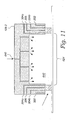
- Figure 11 shows a longitudinal view of the proximity head in accordance with one embodiment of the present invention.
- Figure 12 shows a cross sectional view of a proximity head with the active cavity window in accordance with one embodiment of the present invention.
- Figure 13 illustrates a cross sectional view of a proximity head which includes multiple cavities with multiple menisci in one embodiment of the present invention.
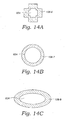
- Figure 14A shows a cross shaped proximity head in accordance with one embodiment of the present invention.
- Figure 14B illustrates a circular shaped proximity head in accordance with one embodiment of the present invention.
- Figure 14C shows an oval shaped proximity head in accordance with one embodiment of the present invention.
- Figure 14D illustrates a strip shaped proximity head in accordance with one embodiment of the present invention.
- Figure 14E shows a wedge shaped proximity head in accordance with one embodiment of the present invention.
- Figure 15A shows an exemplary view of a processing surface of the proximity head in accordance with one embodiment of the present invention.
- Figure 15B illustrates an exemplary view of a processing surface of the proximity head in accordance with one embodiment of the present invention.
- the proximity head utilizes siphon to remove fluid(s) from the fluid meniscus.
- the proximity head includes an active cavity that is surrounded by a fluid meniscus thereby generating a processing region that is highly controllable.
- the region after processing, can be processed using another wafer processing operation (e.g., rinsing) very soon after the initial processing of the region by the active cavity because the fluid meniscus surrounds the active cavity.
- This technology may be utilized to perform any suitable type of combination of types of wafer operation(s) such as, for example drying, etching, plating, etc.
- the systems and proximity heads as described herein are exemplary in nature, and that any other suitable types of configurations that would enable the generation and movement of a meniscus or enable a meniscus with a cavity enclosed therein may be utilized.
- the proximity head(s) may move in a linear fashion from a center portion of the wafer to the edge of the wafer. It should be appreciated that other embodiments may be utilized where the proximity head(s) move in a linear fashion from one edge of the wafer to another diametrically opposite edge of the wafer, or other non-linear movements may be utilized such as, for example, in a radial motion, in a circular motion, in a spiral motion, in a zig-zag motion, in a random motion, etc.
- the motion may also be any suitable specified motion profile as desired by a user.
- the wafer may be rotated and the proximity head moved in a linear fashion so the proximity head may process all portions of the wafer. It should also be understood that other embodiments may be utilized where the wafer is not rotated but the proximity head is configured to move over the wafer in a fashion that enables processing of all portions of the wafer. In other embodiments, either or both of the wafer and the proximity head do not move depending on the wafer processing operation and the configuration of the proximity head.
- the proximity head may be held stationary and the wafer may be moved to be processed by the fluid meniscus. As with the proximity head, the wafer may move in any suitable motion as long as the desired wafer processing operation is accomplished.
- the proximity head and the wafer processing system as described herein may be utilized to process any shape and size of substrates such as for example, 200 mm wafers, 300 mm wafers, flat panels, etc.
- the size of the proximity head and in turn the sizes of the menisci may vary. In one embodiment, the size of the proximity head and the sizes of the menisci may be larger than a wafer being processed, and in another embodiment, the proximity head and the sizes of the menisci may be smaller than the wafer being processed.
- the menisci as discussed herein may be utilized with other forms of wafer processing technologies such as, for example, brushing, lithography, megasonics, etc. A fluid meniscus can be supported and moved (e.g., onto, off of and across a wafer) with a proximity head.
- FIG. 2 shows a wafer processing system 100 in accordance with one embodiment of the present invention.
- the system 100 includes rollers 102a and 102b which may hold and/or rotate a wafer to enable wafer surfaces to be processed.
- the system 100 also includes proximity heads 106a and 106b that, in one embodiment, are attached to an upper arm 104a and to a lower arm 104b respectively.
- the proximity heads 106a and/or 106b may be any suitable proximity heads as described in further detail in reference to Figures 2 through 15 described herein.
- the term "multi-menisci proximity head” is a proximity head capable of generating one or more fluid menisci. In a one embodiment, a first fluid meniscus is substantially surrounded by a second fluid meniscus.
- the first fluid meniscus and the second fluid meniscus are concentric with the second fluid meniscus surrounding the first fluid meniscus.
- the proximity head may be any suitable apparatus that may generate a fluid meniscus as described herein.
- the upper arm 104a and the lower arm 104b can be part of an assembly which enables substantially linear movement (or in another embodiment a slight arc-like movement) of the proximity heads 106a and 106b along a radius of the wafer.
- the assembly may move the proximity heads 106a and 106b in any suitable user defined movement.
- the arms 104 are configured to hold the proximity head 106a above the wafer and the proximity head 106b below the wafer in close proximity to the wafer. For example, in one exemplary embodiment this may be accomplished by having the upper arm 104a and the lower arm 104b be movable in a vertical manner so once the proximity heads are moved horizontally into a location to start wafer processing, the proximity heads 106a and 106b can be moved vertically to a position in close proximity to the wafer.
- the upper arm 104a and the lower arm 104b may be configured to start the proximity heads 106a and 106b in a position where the menisci are generated before processing and the menisci that has already been generated between the proximity heads 106a and 106 may be moved onto the wafer surface to be processed from an edge area of a wafer 108. Therefore, the upper arm 104a and the lower arm 104b may be configured in any suitable way so the proximity heads 106a and 106b can be moved to enable wafer processing as described herein. It should also be appreciated that the system 100 may be configured in any suitable manner as long as the proximity head(s) may be moved in close proximity to the wafer to generate and control multiple meniscus that, in one embodiment, are concentric with each other.
- close proximity may be any suitable distance from the wafer as long as a menisci may be maintained.
- the proximity heads 106a and 106b (as well as any other proximity head described herein) may each be located between about 0.1 mm to about 10 mm from the wafer to generate the fluid menisci on the wafer surface.
- the proximity heads 106a and 106b may each be located bout 0.5 mm to about 2.0 mm from the wafer to generate the fluid menisci on the wafer surface, and in more preferable embodiment, the proximity heads 106a and 106b (as well as any other proximity head described herein) may be located about 1.5 mm from the wafer to generate the fluid menisci on the wafer surface.
- the system 100, the arms 104 are configured to enable the proximity heads 106a and 106b to be moved from processed to unprocessed portions of the wafer. It should be appreciated that the arms 104 may be movable in any suitable manner that would enable movement of the proximity heads 106a and 106b to process the wafer as desired. In one embodiment, the arms 104 may be motivated by a motor to move the proximity head 106a and 106b along the surface of the wafer. It should be understood that although the wafer processing system 100 is shown with the proximity heads 106a and 106b, that any suitable number of proximity heads may be utilized such as, for example, 1, 2, 3, 4, 5, 6, etc.
- the proximity heads 106a and/or 106b of the wafer processing system 100 may also be any suitable size or shape as shown by, for example, any of the proximity heads as described herein.
- the different configurations described herein generate the fluid menisci between the proximity head and the wafer.
- the fluid menisci may be moved across the wafer to process the wafer by applying fluid to the wafer surface and removing fluids from the surface. In such a way, depending on the fluids applied to the wafer, cleaning, drying, etching, and/or plating may be accomplished.
- the first fluid meniscus may conduct one type of operation and the second fluid meniscus that at least partially surrounds the first fluid meniscus may conduct the same operation or a different wafer processing operation as the first fluid meniscus.
- the proximity heads 106a and 106b can have any numerous types of configurations as shown herein or other configurations that enable the processes described herein. It should also be appreciated that the system 100 may process one surface of the wafer or both the top surface and the bottom surface of the wafer.
- the system 100 may also be configured to process one side of the wafer with one type of process (e.g., etching, cleaning, drying, plating, etc.) and process the other side of the wafer using the same process or a different type of process by inputting and outputting different types of fluids or by using a different configuration menisci.
- the proximity heads can also be configured to process the bevel edge of the wafer in addition to processing the top and/or bottom of the wafer. This can be accomplished by moving the menisci off (or onto) the edge the wafer which processes the bevel edge. It should also be understood that the proximity heads 106a and 106b may be the same type of apparatus or different types of proximity heads.
- the wafer 108 may be held and rotated by the rollers 102a and 102b in any suitable orientation as long as the orientation enables a desired proximity head to be in close proximity to a portion of the wafer 108 that is to be processed.
- the rollers 102a and 102b can rotate in a clockwise direction to rotate the wafer 108 in a counterclockwise direction. It should be understood that the rollers may be rotated in either a clockwise or a counterclockwise direction depending on the wafer rotation desired.
- the rotation imparted on the wafer 108 by the rollers 102a and 102b serves to move a wafer area that has not been processed into close proximity to the proximity heads 106a and 106b.
- the rotation itself does not dry the wafer or move fluid on the wafer surfaces towards the edge of the wafer. Therefore, in an exemplary wafer processing operation, the unprocessed areas of the wafer would be presented to the proximity heads 106a and 106b through both the linear motion of the proximity heads 106a and 106b and through the rotation of the wafer 108.
- the wafer processing operation itself may be conducted by at least one of the proximity heads. Consequently, in one embodiment, processed portions of the wafer 108 would expand from a center region to the edge region of the wafer 108 in a spiral movement as the processing operation progresses.
- the processed portions of the wafer 108 would expand from the edge region of the wafer 108 to the center region of the wafer 108 in a spiral movement.
- the proximity heads 106a and 106b may be configured to dry, clean, etch, and/or plate the water 108.
- the at least one of first inlet may be configured to input deionized water (DIW) (also known as a DIW inlet)
- the at least one of a second inlet may be configured to input N 2 carrier gas containing isopropyl alcohol (IPA) in vapor form (also known as IPA inlet)
- the at least one outlet may be configured to remove fluids from a region between the water and a particular proximity head.
- DIW deionized water
- IPA isopropyl alcohol
- the at least one outlet may be configured to remove fluids from a region between the water and a particular proximity head.
- vacuum may be applied through the at least one outlet (also known as vacuum outlet).
- a method such as siphon may be utilized. Siphoning of fluid through the at least one outlet is described in further detail in reference to Figure 8 . It should be appreciated that although IPA vapor is used in some of the exemplary embodiments, any other type of vapor may be utilized such as for example, nitrogen, any suitable alcohol vapor, organic compounds, volatile chemicals, etc. that may be miscible with water.
- a cleaning solution may be substituted for the DIW.
- An exemplary etching embodiment may be conducted where an etchant may be substituted for the DIW.
- plating may be accomplished as described by the methodology herein.
- other types of solutions may be inputted into the first inlet and the second inlet depending on the processing operation desired.
- the inlets and outlets located on a face of the proximity head may be in any suitable configuration as long as stable menisci as described herein may be utilized.
- the at least one N 2 /IPA vapor inlet may be adjacent to the at least one vacuum outlet which is in turn adjacent to the at least one processing fluid inlet to form an IPA-vacuum-processing fluid orientation.
- Such a configuration can generate an outside meniscus that at least partially surrounds the inside meniscus.
- the inside meniscus may be generated through a configuration with a processing fluid-vacuum orientation.
- one exemplary embodiment where a second fluid meniscus at least partially surrounds a first fluid meniscus may be generated by an IPA-vacuum-second processing fluid-vacuum-first processing fluid-vacuum-second processing fluid-vacuum-IPA orientation as described in further detail below.
- IPA-vacuum-second processing fluid-vacuum-first processing fluid-vacuum-second processing fluid-vacuum-IPA orientation may be utilized depending on the wafer processes desired and what type of wafer processing mechanism is sought to be enhanced.
- the IPA-vacuum-processing fluid orientation may be utilized to intelligently and powerfully generate, control, and move the menisci located between a proximity head and a wafer to process wafers.
- the processing fluid inlets, the N 2 /IPA vapor inlets, and the vacuum outlets may be arranged in any suitable manner if the above orientation is maintained.
- the exact configuration of the inlet and outlet orientation may be varied depending on the application. For example, the distance between the IPA input, vacuum, and processing fluid inlet locations may be varied so the distances are consistent or so the distances are inconsistent.
- the distances between the IPA input, vacuum, and processing fluid outlet may differ in magnitude depending on the size, shape, and configuration of the proximity head 106a and the desired size of a process menisci (i.e., menisci shape and size).
- exemplary IPA-vacuum-processing fluid orientation may be found as described further herein. It should be appreciated that anywhere vacuum is utilized to remove fluid from the wafer surface, siphoning as described in further detail in reference to Figure 8 may be utilized for substantially single phase fluids.
- the proximity heads 106a and 106b may be positioned in close proximity to a top surface and a bottom surface respectively of the wafer 108 and may utilize the IPA and DIW inlets and a vacuum outlets as described herein to generate wafer processing menisci in contact with the wafer 108 which are capable of processing the top surface and the bottom surface of the wafer 108.
- the wafer processing menisci may be generated in a manner consistent with the descriptions herein.
- a vacuum may be applied in close proximity to the wafer surface to remove the IPA vapor, the processing fluid, and/or the fluids that may be on the wafer surface.
- IPA IPA
- any other suitable type of vapor such as for example, nitrogen, any suitable alcohol vapor, organic compounds, hexanol, ethyl glycol, acetone, etc. that may be miscible with water. These fluids may also be known as surface tension reducing fluids.
- the portion of the processing fluid that is in the region between the proximity head and the wafer is the menisci.
- the term "output" can refer to the removal of fluid from a region between the wafer 108 and a particular proximity head, and the term “input” can be the introduction of fluid to the region between the wafer 108 and the particular proximity head.
- the proximity heads 106a and 106b may be scanned over the wafer 108 while being moved at the end of an arm that is being moved in a slight arc.
- Figure 3 illustrates a proximity head 106 performing a wafer processing operation in accordance with one embodiment of the present invention.
- Figures 3 through 4B show a method of generating a basic fluid meniscus while Figures 5A through 15B discuss apparatuses and methods for generating a more complex menisci configuration.
- the proximity head 106 in one embodiment, moves while in close proximity to a top surface 108a of the wafer 108 to conduct a wafer processing operation. It should be appreciated that the proximity head 106 may also be utilized to process (e.g., clean, dry, plate, etch, etc.) a bottom surface 108b of the wafer 108.
- the wafer 108 is rotating so the proximity head 106 may be moved in a linear fashion along the head motion while the top surface 108a is being processed.
- the IPA 310 through the inlet 302
- the vacuum 312 through outlet 304, and the processing fluid 314 through the inlet 306 the meniscus 116 may be generated.
- the orientation of the inlets/outlets as shown in Figure 3 is only exemplary in nature, and that any suitable inlets/outlets orientation that may produce a stable fluid meniscus may be utilized such as those configurations as described herein.
- Figure 4A illustrates a wafer processing operation that may be conducted by a proximity head 106a in accordance with one embodiment of the present invention.
- Figure 4A shows a top surface 108a being processed, it should be appreciated that the wafer processing may be accomplished in substantially the same way for the bottom surface 108b of the wafer 108.
- the inlet 302 may be utilized to apply isopropyl alcohol (IPA) vapor toward a top surface 108a of the wafer 108
- the inlet 306 may be utilized to apply a processing fluid toward the top surface 108a of the wafer 108.
- IPA isopropyl alcohol
- the outlet 304 may be utilized to apply vacuum to a region in close proximity to the wafer surface to remove fluid or vapor that may located on or near the top surface 108a.
- the IPA may be in any suitable form such as, for example, IPA vapor where IPA in vapor form is inputted through use of a N 2 gas.
- any suitable fluid used for processing the wafer e.g., cleaning fluid, drying fluid, etching fluid, plating fluid, etc.
- cleaning fluid, drying fluid, etching fluid, plating fluid, etc. may be utilized that may enable or enhance the wafer processing.
- an IPA inflow 310 is provided through the inlet 302
- a vacuum 312 may be applied through the outlet 304 and processing fluid inflow 314 may be provided through the inlet 306. Consequently, if a fluid film resides on the wafer 108, a first fluid pressure may be applied to the wafer surface by the IPA inflow 310, a second fluid pressure may be applied to the wafer surface by the processing fluid inflow 314, and a third fluid pressure may be applied by the vacuum 312 to remove the processing fluid, IPA and the fluid film on the wafer surface.
- IPA IPA/processing fluid interface 118
- the IPA/processing fluid interface 1 18 reduces the surface of tension of the processing fluid.
- the processing fluid is applied toward the wafer surface and almost immediately removed along with fluid on the wafer surface by the vacuum applied by the outlet 304.
- the processing that is applied toward the wafer surface and for a moment resides in the region between a proximity head and the wafer surface along with any fluid on the wafer surface forms a meniscus 116 where the borders of the meniscus 116 are the IPA/processing fluid interfaces 1 18. Therefore, the meniscus 116 is a constant flow of fluid being applied toward the surface and being removed at substantially the same time with any fluid on the wafer surface.
- the nearly immediate removal of the processing fluid from the wafer surface prevents the formation of fluid droplets on the region of the wafer surface being dried thereby reducing the possibility of contamination on the wafer 108 after the processing fluid has accomplished its purpose depending on the operation (e.g., etching, cleaning, drying, plating, etc.).
- the pressure (which is caused by the flow rate of the IPA) of the downward injection of IPA also helps contain the meniscus 116.
- the flow rate of the N2 carrier gas containing the IPA may assist in causing a shift or a push of processing fluid flow out of the region between the proximity head and the wafer surface and into the outlets 304 (vacuum outlets) through which the fluids may be outputted from the proximity head.
- the push of processing fluid flow is not a process requirement but can be used to optimize meniscus boundary control. Therefore, as the IPA and the processing fluid are pulled into the outlets 304, the boundary making up the IPA/processing fluid interface 118 is not a continuous boundary because gas (e.g., air) is being pulled into the outlets 304 along with the fluids.
- the flow into the outlets 304 is discontinuous.
- This flow discontinuity is analogous to fluid and gas being pulled up through a straw when a vacuum is exerted on combination of fluid and gas. Consequently, as the proximity head 106a moves, the meniscus moves along with the proximity head, and the region previously occupied by the meniscus has been dried due to the movement of the IPA/processing fluid interface 118.
- the any suitable number of inlets 302, outlets 304 and inlets 306 may be utilized depending on the configuration of the apparatus and the meniscus size and shape desired.
- the liquid flow rates and the vacuum flow rates are such that the total liquid flow into the vacuum outlet is continuous, so no gas flows into the vacuum outlet.
- any suitable flow rate may be utilized for the N 2 /IPA, processing fluid, and vacuum as long as the meniscus 116 can be maintained.
- the flow rate of the processing fluid through a set of the inlets 306 is between about 25 ml per minute to about 3,000 ml per minute. In a preferable embodiment, the flow rate of the processing fluid through the set of the inlets 306 is about 800 ml per minute. It should be understood that the flow rate of fluids may vary depending on the size of the proximity head. In one embodiment a larger head may have a greater rate of fluid flow than smaller proximity heads. This may occur because larger proximity heads, in one embodiment, have more inlets 302 and 306 and outlets 304.
- the flow rate of the N 2 /IPA vapor through a set of the inlets 302 is between about 1 liters per minute (SLPM) to about 100 SLPM. In a preferable embodiment, the IPA flow rate is between about 6 and 20 SLPM.
- the flow rate for the vacuum through a set of the outlets 304 is between about 10 standard cubic feet per hour (SCFH) to about 1250 SCFH. In a preferable embodiment, the flow rate for a vacuum though the set of the outlets 304 is about 350 SCFH.
- a flow meter may be utilized to measure the flow rate of the N 2 /IPA, processing fluid, and the vacuum.
- any suitable type of wafer processing operation may be conducted using the meniscus depending on the processing fluid utilized.
- a cleaning fluid such as, for example, SC-1, SC-2, etc.
- different fluids may be utilized and similar inlet and outlet configurations may be utilized so the wafer processing meniscus may also etch and/or plate the wafer.
- etching fluids such as, for example, HF, EKC proprietary solution, KOH etc.
- plating fluids such as, for example, Cu Sulfate, Au Chloride, Ag Sulfate, etc. in conjunction with electrical input may be conducted.
- Figure 4B illustrates a side view of exemplary proximity heads 106 and 106b for use in a dual wafer surface processing system in accordance with one embodiment of the present invention.
- the meniscus 116 may be generated.
- the inlets 302 and 306 may be utilized for IPA inflow 310 and processing fluid inflow 314 respectively while the outlet 304 may be utilized to apply vacuum 312.
- the proximity heads 106 and 106b may be of a configuration as described further herein. Any suitable surface coming into contact with the meniscus 116 such as, for example, wafer surfaces 108a and 108b of the wafer 108 may be processed by the movement of the meniscus 116 into and away from the surface.
- Figures 5A through 7 show embodiments of the present invention where a first fluid meniscus is at least partially surrounded by at least a. second fluid meniscus.
- first fluid meniscus and/or the second fluid meniscus may be generated to conduct any suitable type of substrate/wafer processing operation such as, for example, lithography, etching, plating, cleaning, and drying.
- the first fluid meniscus and the second fluid meniscus may be any suitable shape or size depending on the substrate processing operation desired.
- the first fluid meniscus and the second fluid meniscus are concentric where the second fluid meniscus surrounds the first fluid meniscus and the first fluid meniscus and the second fluid meniscus provide a continuous fluid connection.
- the portion of the wafer processed by the first fluid meniscus is immediately processed by the second fluid meniscus without a substantial amount of the contact with the atmosphere. It should be appreciated that depending on the operation desired, in one embodiment, the first fluid meniscus may contact the second meniscus and in another embodiment, the first fluid meniscus does not directly contact the second meniscus.
- FIG. 5A shows a multi-menisci proximity head 106-1 in accordance with on embodiment of the present invention.
- the multi-menisci proximity head 106-1 includes a plurality of source inlets 306a that can apply a first fluid to the wafer surface.
- the first fluid can then be removed from the wafer surface by application of siphon or vacuum through a plurality of source outlets 304a. Therefore, the first fluid meniscus may be generated by the conduits located within a first fluid meniscus region 402 of the processing surface on the multi-menisci proximity head 106-1.
- the multi-menisci proximity head 106-1 may also include a plurality of source inlets 306b that can apply a second fluid to the wafer surface.
- the second fluid can then be removed from the wafer surface by application of vacuum through a plurality of source outlets 304b.
- a portion of the second fluid is also removed by the plurality of source outlets 304a in conjunction with the removal of the first fluid.
- the plurality of source outlets 304a may be called a one phase fluid removal conduit because the outlets 304a remove liquids applied to the wafer through the source inlets 306a and 306b. In such one phase removal, siphoning and/or vacuum may be utilized.
- the meniscus When siphoning is used, the meniscus may be self regulated because as more fluid is applied to the wafer surface, the more the fluid is removed from the water surface through siphon. Therefore, even at variable flow rates, the siphoning can increase or decrease fluid removal rate depending on the flow rates into the fluid meniscus(es). Siphoning with regard to single phase fluid removal from the wafer surface (e.g., from the meniscus(es) on the wafer surface) is described in further detail in reference to Figure 8 .
- the plurality of source outlets 306b may be called a two phase removal conduit because the outlets 306b removes the second fluid from the source inlets 306b and the atmosphere outside of the fluid meniscus. Therefore, in one embodiment, the outlets 306b removes both liquid and gas while the outlets 306a remove only liquids.
- the second fluid meniscus may be created by the conduits located within a second fluid meniscus region 404 of the processing surface on the multi-meniscus proximity head 106-1.
- the multi-menisci proximity head 106-1 may include a plurality of source inlets 302 which can apply a third fluid to the wafer surface.
- the third fluid may be a surface tension reducing fluid that can reduce the surface tension of a liquid/atmosphere border of the second meniscus formed by that application of the second fluid to the wafer surface.
- the processing surface (e.g., the surface area of the multi-menisci proximity head where the conduits exist) of the multi-menisci proximity head 106-1 may be of any suitable topography such as, for example, flat, raised, lowered.
- the processing surface of the multi-menisci 106-1 may have a substantially flat surface.
- Figure 5B shows a cross section view of the multi-menisci proximity head 106-1 in accordance with one embodiment of the present invention.
- the multi-menisci proximity head 106-1 can apply the first fluid through the plurality of source inlets 306a and remove the first fluid through the plurality of source outlets 304a through use of siphoning and/or vacuum.
- the first fluid meniscus 116a is located underneath a region substantially surrounded by the plurality of source outlets 304a.
- the multi-menisci proximity head 106-a can also apply the second fluid through the plurality of source inlets 306b and remove the second fluid through the plurality of source outlets 304a on one side of the second fluid meniscus and 304b on the other side.
- the plurality of source inlets 302 may apply the third fluid to decrease the surface tension of the fluid making up the second fluid meniscus 116b.
- the plurality of source inlets 302 may be optionally angled to better confine the second fluid meniscus 116b.
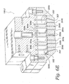
- FIG. 6A illustrates a multi-menisci proximity head 106-2 in accordance with one embodiment of the present invention.
- the proximity head 106-2 includes, in one embodiment, a facilities plate 454 and a body 458. It should be appreciated the proximity head 106-2 may include any suitable numbers and/or types of pieces as long as the first fluid meniscus and the second fluid meniscus as described herein may be generated.
- the facilities plate 454 and the body 458 may be bolted together or in another embodiment, the plate 454 and the body 458 may be attached by an adhesive.
- the facilities plate 454 and the body 458 may be made from the same material or different materials depending on the applications and operations desired by a user.
- the proximity head 106-2 may include a processing surface 458 which includes conduits where fluid(s) may be applied to surface of the wafer and the fluid(s) maybe removed from a surface of the wafer.
- the processing surface 458 may, in one embodiment, be elevated above a surface 453 as shown by an elevated region 452. It should be appreciated that the processing surface 458 does not have to be elevated and that the surface 458 may be substantially planar with the surface 453 of the proximity head 106-2 that faces the surface of the wafer being processed.
- Figure 6B illustrates the processing surface 458 of the proximity head 106-2 in accordance with one embodiment of the present invention.
- the processing surface 458 is a region of the proximity head 106-2 which generates the fluid menisci.
- the processing surface 458 may include any suitable number and type of conduits so the first fluid meniscus and the second fluid meniscus may be generated.
- the processing surface 458 includes fluid inlets 306a, fluid outlets 304a, fluid inlets 306b, fluid outlets 304b, and fluid inlets 302.
- the fluid inlets 306a may apply a first fluid to the surface of the wafer, and the fluid inlets 306b may apply a second fluid to the surface of the wafer.
- the fluid outlets 304a may remove the first fluid and a portion of a second fluid from the surface of the wafer by the application of siphoning and/or vacuum
- the fluid outlets 304b may remove a portion of the second fluid from the surface of the wafer by the application of vacuum
- the fluid inlets 302 may apply a fluid that can decrease the surface tension of the second fluid.
- the first fluid and/or the second fluid may be any suitable fluid that can facilitate any one of a lithography operation, an etching operation, a plating operation, a cleaning operation, a rinsing operation, and a drying operation.
- Figure 6C shows a closer view of the processing surface 458 of the multi-meniscus proximity head 106-2 in accordance with one embodiment of the present invention.
- the processing surface 458 includes a first fluid meniscus region 402 which includes the fluid inlets 306a and fluid outlets 304a.
- the processing surface 458 also includes a second fluid meniscus region 404 includes the fluid inlets 306b and the fluid outlets 304b and the fluid inlets 302. Therefore, the first fluid meniscus region 402 can generate the first fluid meniscus and the second fluid meniscus region 404 can generate the second fluid meniscus.
- Figure 6D shows the facilities plate 454 attaching to the body 456 to form the multi-menisci proximity head 106-2 in accordance with one embodiment of the present invention.
- Channels corresponding to the fluid inlets 306a, 304a, and 302 supply fluid from the facilities plate 454 into the body 456 of the multi-menisci proximity head 106-2, and channels corresponding to the fluid outlets 306b and 304b remove fluid from the body 456 to the facilities 454.
- channels 506a, 504a, 506b, 504b, and 502 correspond to the fluid inlets 306a, fluid outlets 306b, fluid inlets 304a, fluid outlets 304b, and fluid inlets 302.
- FIG. 6E illustrates a cross section view of the proximity head 106-2 in accordance with one embodiment of the present invention.
- channels 506a, 506b, and 502 may supply a first fluid, a second fluid, and a third fluid to fluid inlets 306a, 306b, and 302 respectively.
- a channel 504a may remove a combination of the first fluid and the second fluid from the fluid outlets 304a through use of siphoning and/or vacuum
- channel 504b may remove combination of the second fluid and the third fluid from the outlets 304b.
- the first fluid is a first processing fluid that can conduct any suitable operation on a wafer surface such as, for example, etching, lithography, cleaning, rinsing, and drying.
- the second fluid is a second processing fluid that may or may not be the same as the first fluid.
- the second fluid may be any suitable type of processing fluid such as, for example, a fluid that can facilitate etching, lithography, cleaning, rinsing, and drying.
- Figure 7 illustrates a cross-sectional view of the multi-menisci proximity head in exemplary wafer processing operations in accordance with one embodiment of the present invention.
- Figure 7 shows a top surface of the wafer 108 being processed, it should be appreciated by those skilled in the art that both a top surface and a bottom surface of the wafer 108 may be concurrently processed by any of the proximity heads described herein on the top surface of the wafer 108 and by any of the proximity heads described herein on the bottom surface of the wafer 108.
- a first wafer processing chemistry is applied to the wafer 108 through fluid inlet 306a.
- the first wafer processing chemistry is removed from the wafer surface through the fluid outlet 304a.
- the first wafer processing fluid may form a first fluid meniscus 116a between the multi-menisci proximity head 106-2 and the wafer 108.
- a second processing fluid such as, for example, deionized water (DIW) is applied to the wafer surface through the fluid inlets 306b.
- DIW deionized water
- the second processing fluid may be any suitable fluid that can accomplish the desired operation on the wafer surface.
- the DIW is removed from the wafer surface through both the source outlets 304a and 304b.
- the DIW between the multi-menisci proximity head 106-2 and the wafer surface may form a second fluid meniscus 116b.
- a surface tension reducing fluid such as, for example, isopropyl alcohol vapor in nitrogen gas may optionally be applied from the source inlet 302 to the wafer surface to keep the liquid/gas border of the second fluid meniscus 116b stable.
- the second fluid meniscus 116b can substantially surround the first fluid meniscus 116a. In this way, after the first fluid meniscus 116a has processed the wafer surface, the second fluid meniscus 116b can nearly immediately begin operating on a portion of the wafer surface already processed by the first fluid meniscus 116a. Therefore, in one embodiment, the second fluid meniscus 116b forms a concentric ring around the first fluid meniscus 116a.
- first fluid meniscus 116a may be any suitable geometric shape such as, a circle, ellipse, square, rectangle, triangular, quadrilateral, etc.
- the second fluid meniscus 116b can be configured to at least partially surround whatever shape the first fluid meniscus 116a may be. It should be appreciated that, as discussed above, the first fluid meniscus 116a and/or the second fluid meniscus 116b may utilize any suitable fluid(s) depending on the wafer processing operation desired.
- an amount of the first fluid inputted into the first fluid meniscus through the source inlets 306a should be substantially equal to the amount of the first fluid removed through the source outlets 304a.
- the amount of the second fluid inputted into the second fluid meniscus through the source inlets 306b should be substantially equal to the amount of the second fluid removed through the source outlets 304a and 304b.
- the flow rates of the fluids are determined by a distance 480 the proximity head 106-2 is off of the wafer 108. It should be appreciated that the distance 480 may be any suitable distance as long as the menisci can be maintained and moved in a stable manner.
- the distance 480 may be between 50 microns and 5 mm, and in another embodiment .5 mm to 2.5 mm.
- the distance 480 is between about 1 mm and 1.5 mm. In one embodiment, the distance 480 is about 1.3.
- the flow rates of the fluids as shown in Figure 7 may be any suitable flow rate that can generate the first fluid meniscus and the second fluid meniscus that substantially surrounds the first meniscus. Depending on the distinction desired between the first fluid meniscus and the second fluid meniscus, the flow rates may differ.
- source inlets 306a may apply the first fluid at a flow rate of about 600 cc/min
- source inlets 306b may apply the second fluid at a flow rate of about 900 cc/min
- a source outlets 304a may remove the first fluid and the second fluid at a flow rate of about 1200 cc/min
- the source outlets 304b may remove the second fluid and atmosphere (which may include some IPA vapor in N 2 if such a surface tension reducing fluid is being applied to the wafer surface) at a flow rate of about 300 cc/min.
- the flow rate of fluids through the source outlets 304 may equal 2 times the flow rate of fluid through the source inlets 306a.
- the flow rate of fluid through the source inlets 306b may be equal to the flow rate through the source inlets 306a plus 300. It should be appreciated by those skilled in the art that specific flow rate relationships of the source inlets 306a, 306b and source inlets 304a, 304b may change depending on the configuration of the process area and/or the configuration of the proximity heads described herein.
- the optimal flow rate is automatically generated thereby creating a self regulating meniscus where the flow rate of fluid from the meniscus to the source outlets 304 is automatically adjusted depending on the flow rates through the source inlets 306a and 306b.
- the siphon can keep operating to self regulate the shape and size of the fluid meniscus.
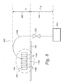
- FIG. 8 illustrates a siphoning system 500 in accordance with one embodiment of the present invention.
- siphoning may be used to control fluid removal through the source outlet(s) (e.g., inner return flow).
- source outlet(s) e.g., inner return flow
- vacuum is not utilized therefore, the flow of fluid from the fluid meniscus is made independent from fluctuations in the clean dry air generating the vacuum in a vacuum tank. This generates enhanced stability of the inner return flow which results in greater stability of the overall meniscus.
- the meniscus may become self regulating and therefore be more robust.
- the siphoning system 500 includes at least one siphon tube 548 coupled to the proximity head 106.
- the one or more siphon tubes 548 may be coupled to the proximity head 106 to remove fluid from fluid meniscus(es) generated by the proximity head 106.
- the siphon tubes 548 are connected at the other end to a receiving tank 560 where fluids removed from the proximity head 106 may be outputted from the siphon tubes 548.
- the receiving tank is at a lower elevation than the proximity head 106 which promotes the siphoning action.
- the siphoning system 500 is structured so the gravitational force corresponding to the vertical distance 580 is less than the gravitational force corresponding to the vertical distance 582.
- the maximum siphon flow can be regulated by conductance of plumbing from the proximity head 106 to the receiving tank 560. Therefore, specific siphon flow rates can be achieved via the use of flow restrictor 550 in the line. Fixed restriction of the flow restrictor 550 can therefore result in set and forget siphon flow rates. In addition, variable restrictions of the flow restrictor 550 may be used for tunable control of the siphon flow.
- the flow restrictor 550 may be any suitable device such as, for example, a valve that can control fluid flow.
- a siphon flow can be induced via tank vacuum to charge a dry line.
- the siphon tube 548 may be charged by applying vacuum and thereby filling the siphon tube 548 with liquid from a fluid meniscus generated by the proximity head 106. Once the siphon tube 548 is filled with liquid, the vacuum may pull the fluid in the siphon tube 548 to the receiving tank 560. Once the flow has started the tank vacuum in the receiving tank 560 may be eliminated and the siphon action facilitates the fluid flow through the siphon tube 548.
- the restrictor 550 may be a shut-off valve could be used to start and stop the flow without assistance of tank vacuum. If the siphon tube 548 is charged (e.g., filled with liquid), opening the valve starts siphon flow. If the siphon tube 548 is dry, then it could be charged first with fluid and then the siphon flow would begin as soon as the valve is opened. Therefore, in one embodiment, siphon flow can be used for all single-phase liquid lines in the system. In addition, siphon flow is operable with air bubbles as long as the line is substantially filled with liquid.
- the siphoning system 500 may be utilized with any suitable proximity head 106 that has a fluid return system that removes a single phase fluid such as liquids.
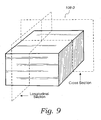
- Figure 9 illustrates a proximity head 106-3 with an active cavity in accordance with one embodiment of the present invention.
- the proximity head 106-3 has a cross section that is described in further detail in reference to Figure 10 and a longitudinal section that is described in further detail in reference to Figure 11 .
- An exemplary processing surface of the proximity head 106-3 is discussed in further detail in reference to Figure 15A .
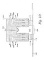
- Figure 10 shows a cross section of the proximity head 106-3 in operation in accordance with one embodiment of the present invention.
- the proximity head 106-3 includes a source inlet 640 into a cavity 642.
- the cavity 642 may be any suitable shape and may take up any suitable volume within the proximity head 106-3 as long as the active agent may be inputted into the cavity 642 and the active agent may be applied to the wafer surface through an opening (e.g., active cavity window 624).
- the opening to the cavity 642 is substantially surrounded by the fluid meniscus 116 generated by the application of fluid to the wafer surface by the source inlets 306 and by the removal of the fluid from the fluid meniscus 116 by the source outlets 304a and 304b.
- the cavity 642 may be used to deliver active agents to the wafer surface via the active cavity window 624.
- the active cavity window 624 may be any suitable size and/or shape depending on the size and shape of the region of the wafer surface desired to be processed.
- the active cavity window 624 defines the opening to the cavity 642.
- the wafer surface within the active cavity window 624 that is processed by the active agents is known as an active region.
- the active agent may be any suitable liquid, gas, vapor, or other form of chemistry (e.g., foam) that can process the wafer.
- the active agent may include substances such as, for example, ozone, chelating agents (e.g., EDTA, etc.), cleaning chemistries (e.g., SC1, SC2, etc.), semi-aqueous solvents (e.g., ATMI ST-255 and ATMI PT-15 (made by ATMI of Danbury, CT), EKC5800TM (made by EKC Technology in Danville, CA, etc.), HF, etc.).
- the active agents can be dispensed via the source inlet 640 which in one embodiment may include nozzles (e.g., flat fan, cone spray, mist/fogger). It should be appreciated that the source inlet 640 may be any suitable type of opening that can transport the active agent into the cavity 642.
- the active agents may be rinsed or otherwise removed by the meniscus 116 that surrounds the active cavity window 624.
- the wafer 108 may be dry in and dry out meaning that the wafer may, in one embodiment, be dry before wafer processing and substantially dry after wafer processing even though the wafer surface has been treated by active agents in the active cavity window 624. Therefore, the active agents can be confined to the cavity within the proximity head 106-3.
- ozone (or other oxidizing gas) may be introduced into the cavity 642 and the wafer surface in the active cavity window 624 is wetted by the meniscus 116 which may be a heated DIW rinse meniscus.
- the ozone in this case may react with and remove organic material from the wafer surface through the wafer boundary layer. This may be used in operation such as, for example, strip photoresist operations.
- conduit i.e., outlets and inlets
- proximity head structure utilized in Figure 10 as well as the other conduit patterns and proximity head structures discussed herein are only exemplary in nature and that the proximity head discussed herein encompasses any suitable proximity head structure that may be utilized that can generate a fluid meniscus substantially around a region of the substrate surface where active agents can conduct substrate processing.
- FIG 11 shows a longitudinal view of the proximity head 106-3 in accordance with one embodiment of the present invention.
- the proximity head 106-3 include source inlets 640 into the cavity 642.
- four source inlets 640 are defined within the longitudinal section of the proximity head 106-3. It should be appreciated that depending on the wafer processing operation desired and the amount of active agents desired to be inputted into the cavity 642, any suitable number of source inlets 640 may be included in the proximity head 106-3 such as, for, example, 1, 2, 3, 4, 5, 6, 7, 8, 9, 10, etc.
- the proximity head in the longitudinal view includes source inlets 306 and source outlets 304a and 304 as well as source inlets 302 for generating the fluid meniscus 116.
- the source inlets 306 may apply a processing fluid (e.g., rinsing fluid) to the wafer surface. The processing fluid may be removed from the wafer surface by the source outlet 304a and 304b.
- source inlet 302 is optionally included in the proximity head 106-3 and depending on the proximity head 106-3 configuration, a stable fluid meniscus may be generated without usage of the source inlets 302.
- a surface tension reducing fluid may be applied to the wafer surface and the outer border of the fluid meniscus 116. Consequently, the fluid meniscus 116 generated surrounds the active cavity window 624.
- Figure 12 shows a cross sectional view of a proximity head 106-4 with the active cavity window 624 in accordance with one embodiment of the present invention. It should be appreciated that the cross sectional view shown in Figure 12 is another embodiment of the cross sectional view discussed above in reference to Figure 10 .
- the cross sectional view of the proximity head 106-4 includes a source inlet 640 that can input an active agent into the cavity 624. The active agent can then process an active region of the substrate surface that is defined by the active cavity window 624.
- the cross sectional view of the proximity head 106-4 also includes source inlets 306 and source outlets 304a, 304b, and 304c.
- the proximity head 106-4 can apply a fluid through the source inlets 306 to the surface of the wafer to a region substantially surrounding the active region.
- the source outlets 304a, 304b, and 304c can remove the fluid from the surface of the wafer substantially surrounding the active region. This application and removal of fluid may generate the fluid meniscus that can substantially surround the active region.
- an active agent can be applied to process the active region of the wafer surface and afterwards with either one of wafer or proximity head movement, the fluid meniscus 116 may further process (e.g., clean, rinse, etch, etc.) the wafer surface in the active region.
- the source outlet 304a may utilize vacuum to remove fluids from the wafer surface.
- the source outlet 304a may remove the fluid applied by the source inlets 304a as well as the fluids and/or materials remaining from the active agent processing of the active region of the wafer surface.
- the source outlet 304b in this embodiment may be a single phase meniscus removal conduit.
- the source outlet 304b may use vacuum and/or siphoning to remove the fluid making up the fluid meniscus 116.
- the source outlet 304c in this embodiment may utilize vacuum to remove the fluid from an outer region of the fluid meniscus 116 to define the outside border of the fluid meniscus 116.
- Figure 13 illustrates a cross sectional view of a proximity head 106-5 which includes multiple cavities with multiple menisci in one embodiment of the present invention.
- the cross section view of the proximity head 106-5 is another embodiment of the cross section view as discussed in reference to Figure 10 .
- the source inlets and outlets such as, for example, source inlet 306b and source outlets 304c and 304d of the cross sectional view may extend into a z-axis. It should be appreciated that any suitable plumbing of the source inlets and outlets may be utilized that can generate the fluid menisci consistent with the methodologies and descriptions herein.
- the proximity head 106-5 includes multiple cavities 642a and 642b.
- the proximity heads described herein may contain any suitable number of cavities such as, for example, 1, 2, 3, 4, 5, 6, 7, 8, 9, 10, etc. depending on the wafer processing operation desired. It should be appreciated that the cavities 642a and 642b may be any suitable shape and may be located in any suitable place as long as the openings to the cavities may be substantially surrounded by fluid menisci.
- the proximity head 106-5 can include source inlets 304b to apply fluid to a wafer surface and source outlets 304c and 304d to remove fluid from the wafer surface to generate a fluid meniscus 116c.
- the proximity head 106-5 may also include source inlets 306a and source outlets 304a and 304b may generate the fluid meniscus 116b substantially surrounding the active region defined by the active cavity window 624a.
- the proximity head 106-5 may further include source inlets 306c and source outlets 304e and 304f to generate the fluid meniscus 116b which can substantially surround the active cavity window 624.
- the proximity head 106-5 may apply an active agent into the cavities 642a and 642b from the source inlets 640a and 640b respectively.
- An exemplary processing surface of the proximity head 106-5 is discussed in further detail in reference to Figure 15B .
- Figures 14A through 14E illustrate exemplary proximity head structures. It should be appreciated that the active cavity windows in all of the embodiments are substantially surrounded by conduits that may generate a fluid meniscus substantially surrounding the active cavity windows.
- Figure 14A shows a cross shaped proximity head 106-6 in accordance with one embodiment of the present invention.
- the active cavity window 624 is in a shape of a cross.
- the proximity head 106-6 may be configured to generate the fluid meniscus 116 around the active cavity window 624.
- Figure 14B illustrates a circular shaped proximity head 106-7 in accordance with one embodiment of the present invention.
- the active cavity window 624 is a circular shape.
- the proximity head 106-7 may be configured to generate the fluid meniscus 116 around the active cavity window 624.
- Figure 14C shows an oval shaped proximity head 106-8 in accordance with one embodiment of the present invention.
- the active cavity window 624 is an oval shape.
- the proximity head 106-8 may be configured to generate the fluid meniscus 116 around the active cavity window 624.
- Figure 14D illustrates a strip shaped proximity head 106-9 in accordance with one embodiment of the present invention.
- the active cavity window 624 is a strip shape.
- the proximity head 106-9 may be configured to generate the fluid meniscus 116 around the active cavity window 624.
- Figure 14E shows a wedge shaped proximity head 106-10 in accordance with one embodiment of the present invention.
- the active cavity window 624 is a wedge shape.
- the proximity head 106-10 may be configured to generate the fluid meniscus 116 around the active cavity window 624.
- FIG 15A shows an exemplary view of a processing surface 700 of the proximity head 106-3 in accordance with one embodiment of the present invention.
- the processing surface 700 includes the cavity 642 as discussed in further detail in reference to Figures 10 and 11 .
- the processing surface 700 may also include a region 701 substantially surrounding the openings to the cavity 642 which may include a plurality of conduits that can generate the fluid meniscus 116 such as, for example, source inlets 306 and source outlets 304a and 304b as discussed in further detail in reference to Figures 10 and 11 .
- the plurality of conduits may surround the cavity 642.
- Figure 15B illustrates an exemplary view of a processing surface 704 of the proximity head 106-5 in accordance with one embodiment of the present invention.
- the processing surface 704 may include the cavities 642a and 642b as discussed in further detail in reference to Figure 13 .
- the proximity head 106-5 may also include regions 702, 706, and 704 which may substantially surround the opening to the cavities.
- the regions 702, 706, and 704 include a plurality of conduits that can generate the fluid menisci 116a, 116c, and 116b.
- the plurality of conduits may include source inlets 306a, 306b, and 306c as well as source outlets 304a, 304b, 304c, 304d, 304e, and 304f as discussed in further detail in reference to Figure 13 .
Landscapes
- Engineering & Computer Science (AREA)
- Condensed Matter Physics & Semiconductors (AREA)
- General Physics & Mathematics (AREA)
- Manufacturing & Machinery (AREA)
- Computer Hardware Design (AREA)
- Microelectronics & Electronic Packaging (AREA)
- Power Engineering (AREA)
- Physics & Mathematics (AREA)
- Cleaning Or Drying Semiconductors (AREA)
- Weting (AREA)
- Mechanical Treatment Of Semiconductor (AREA)
- Exposure Of Semiconductors, Excluding Electron Or Ion Beam Exposure (AREA)
- Drying Of Semiconductors (AREA)
- Details Or Accessories Of Spraying Plant Or Apparatus (AREA)
- Lubrication Of Internal Combustion Engines (AREA)
- Magnetically Actuated Valves (AREA)
- Water Treatment By Sorption (AREA)
Claims (17)
- Vorrichtung zur Bearbeitung eines Substrats, die umfasst:einen Nähekopf (106), der so ausgelegt ist, dass er sich in der Nähe einer Oberfläche des Substrats (108) befindet, wenn er in Betrieb ist;eine Öffnung an einer Oberfläche des Nähekopfs zu einem Hohlraum (642), der im Nähekopf (106) definiert ist, wobei der Hohlraum dazu ausgelegt ist, ein aktives Gas zur Oberfläche des Substrats (108) durch die Öffnung hindurch zu liefern; undeine Vielzahl von Kanälen (304, 306) an der Oberfläche des Nähekopfs, die dazu ausgelegt sind, einen Fluidmeniskus (116) auf der Oberfläche des Substrats (108), der die Öffnung umgibt, zu erzeugen;wobei der Fluidmeniskus (116) die Oberfläche des Substrats (108) bearbeitet;dadurch gekennzeichnet, dass die Vielzahl von Kanälen (304, 306) eine Vielzahl von Einlässen und eine Vielzahl von Auslässen, die die Öffnung in den Hohlraum umgeben, umfasst; und wobei der mindestens eine Einlass (640) des Hohlraums so definiert ist, dass er das aktive Gas in den Hohlraum einbringt.
- Vorrichtung zur Bearbeitung eines Substrats nach Anspruch 1, wobei die Vielzahl von Kanälen (304, 306) einen Einlass (306), um ein Fluid auf die Oberfläche des Substrats aufzubringen, und einen Auslass (304), um das Fluid von der Oberfläche des Substrats zu entfernen, umfasst.
- Vorrichtung zur Bearbeitung eines Substrats nach Anspruch 2, wobei das Fluid entweder ein lithographisches Fluid, ein Ätzfluid, ein Plattierungsfluid, ein Reinigungsfluid oder ein Spülfluid ist.
- Vorrichtung zur Bearbeitung eines Substrats nach Anspruch 2, wobei die Vielzahl von Kanälen (304, 306) ferner einen zusätzlichen Einlass umfasst, um ein die Oberflächenspannung verringerndes Fluid auf die Oberfläche des Substrats aufzubringen.
- Vorrichtung zur Bearbeitung eines Substrats nach Anspruch 1, wobei das aktive Mittel ein Gas, eine Flüssigkeit und/oder ein Dampf ist.
- Verfahren zur Bearbeitung eines Substrats, das umfasst:Aufbringen eines aktiven Mittels auf einen aktiven Bereich einer Oberfläche des Substrats (108);Erzeugen eines Fluidmeniskus (116) auf der Oberfläche des Substrats mit einem Nähekopf, wobei der Fluidmeniskus den aktiven Bereich umgibt;gekennzeichnet durch:Bearbeiten der Oberfläche des Substrats (108) mit dem aktiven Mittel;Bearbeiten der Oberfläche des Substrats mit dem Fluidmeniskus (116); undwobei der aktive Bereich durch eine Öffnung an der Oberfläche des Substrats definiert ist, wobei die Öffnung in einen Hohlraum verläuft, der innerhalb des Nähekopfs definiert ist.
- Verfahren zur Bearbeitung eines Substrats nach Anspruch 6, wobei die Bearbeitung der Oberfläche des Substrats (108) mit dem aktiven Mittel entweder einen Ätzvorgang, einen Reinigungsvorgang, einen Spülvorgang, einen Plattierungsvorgang oder einen Lithographievorgang umfasst.
- Verfahren zur Bearbeitung eines Substrats nach Anspruch 6, wobei die Bearbeitung der Oberfläche des Substrats (108) mit dem Fluidmeniskus (116) entweder einen Ätzvorgang, einen Reinigungsvorgang, einen Spülvorgang, einen Plattierungsvorgang, einen Trocknungsvorgang oder einen Lithographievorgang umfasst.
- Verfahren zur Bearbeitung eines Substrats nach Anspruch 6, wobei das Erzeugen des Fluidmeniskus (116) das Aufbringen eines Fluids auf die Oberfläche des Substrats (108) durch einen Fluideinlass und das Entfernen des Fluids von der Oberfläche des Substrats durch einen Fluidauslass umfasst.
- Verfahren zur Bearbeitung eines Substrats nach Anspruch 9, wobei das Fluid entweder ein lithographisches Fluid, ein Ätzfluid, ein Plattierungsfluid, ein Reinigungsfluid oder ein Spülfluid ist.
- Verfahren zur Bearbeitung eines Substrats nach Anspruch 8, wobei das Erzeugen des Fluidmeniskus (116) ferner das Aufbringen eines zusätzlichen Fluids auf die Oberfläche des Substrats durch einen zusätzlichen Einlass umfasst, wobei das zusätzliche Fluid ein die Oberflächenspannung verringerndes Fluid ist.
- Verfahren zur Bearbeitung eines Substrats nach Anspruch 9, wobei das Entfernen des Fluids das Absaugen des Fluids in einen Behälter umfasst, der in der Höhe niedriger liegt als der Nähekopf.
- Verfahren zur Bearbeitung eines Substrats nach Anspruch 6, das ferner umfasst:Erzeugen eines zweiten Fluidmeniskus auf der Oberfläche des Substrats, wobei der zweite Fluidmeniskus zum ersten Fluidmeniskus benachbart ist, wobei das Erzeugen des ersten Fluidmeniskus und des zweiten Fluidmeniskus das Absaugen zumindest des ersten Fluids vom ersten Fluidmeniskus umfasst.
- Verfahren zur Bearbeitung eines Substrats nach Anspruch 13, wobei das Absaugen das Entfernen zumindest des ersten Fluids von der Oberfläche des Substrats durch ein Rohr in einen Behälter umfasst, der in der Höhe niedriger liegt als der Nähekopf.
- Verfahren zur Bearbeitung eines Substrats nach Anspruch 14, wobei das Absaugen durch Füllen des Rohrs mit zumindest dem ersten Fluid begonnen wird.
- Verfahren zur Bearbeitung eines Substrats nach Anspruch 14, wobei das Rohr durch ein Vakuum gefüllt wird.
- Verfahren zur Bearbeitung eines Substrats nach Anspruch 13, wobei der erste Fluidmeniskus selbstregulierend ist.
Applications Claiming Priority (2)
| Application Number | Priority Date | Filing Date | Title |
|---|---|---|---|
| US10/883,301 US6954993B1 (en) | 2002-09-30 | 2004-06-30 | Concentric proximity processing head |
| US10/956,799 US7093375B2 (en) | 2002-09-30 | 2004-09-30 | Apparatus and method for utilizing a meniscus in substrate processing |
Publications (3)
| Publication Number | Publication Date |
|---|---|
| EP1612847A2 EP1612847A2 (de) | 2006-01-04 |
| EP1612847A3 EP1612847A3 (de) | 2007-11-28 |
| EP1612847B1 true EP1612847B1 (de) | 2010-11-17 |
Family
ID=34978730
Family Applications (1)
| Application Number | Title | Priority Date | Filing Date |
|---|---|---|---|
| EP05253885A Not-in-force EP1612847B1 (de) | 2004-06-30 | 2005-06-22 | Reinigungsapparat |
Country Status (9)
| Country | Link |
|---|---|
| US (2) | US7093375B2 (de) |
| EP (1) | EP1612847B1 (de) |
| JP (2) | JP5013685B2 (de) |
| KR (1) | KR101157847B1 (de) |
| AT (1) | ATE488863T1 (de) |
| DE (1) | DE602005024745D1 (de) |
| MY (1) | MY138656A (de) |
| SG (1) | SG118400A1 (de) |
| TW (1) | TWI292176B (de) |
Families Citing this family (164)
| Publication number | Priority date | Publication date | Assignee | Title |
|---|---|---|---|---|
| US7584761B1 (en) * | 2000-06-30 | 2009-09-08 | Lam Research Corporation | Wafer edge surface treatment with liquid meniscus |
| US7234477B2 (en) | 2000-06-30 | 2007-06-26 | Lam Research Corporation | Method and apparatus for drying semiconductor wafer surfaces using a plurality of inlets and outlets held in close proximity to the wafer surfaces |
| US20040031167A1 (en) | 2002-06-13 | 2004-02-19 | Stein Nathan D. | Single wafer method and apparatus for drying semiconductor substrates using an inert gas air-knife |
| US8236382B2 (en) * | 2002-09-30 | 2012-08-07 | Lam Research Corporation | Proximity substrate preparation sequence, and method, apparatus, and system for implementing the same |
| US7153400B2 (en) * | 2002-09-30 | 2006-12-26 | Lam Research Corporation | Apparatus and method for depositing and planarizing thin films of semiconductor wafers |
| US7520285B2 (en) * | 2002-09-30 | 2009-04-21 | Lam Research Corporation | Apparatus and method for processing a substrate |
| US7367345B1 (en) | 2002-09-30 | 2008-05-06 | Lam Research Corporation | Apparatus and method for providing a confined liquid for immersion lithography |
| US7389783B2 (en) * | 2002-09-30 | 2008-06-24 | Lam Research Corporation | Proximity meniscus manifold |
| US7293571B2 (en) | 2002-09-30 | 2007-11-13 | Lam Research Corporation | Substrate proximity processing housing and insert for generating a fluid meniscus |
| US7997288B2 (en) * | 2002-09-30 | 2011-08-16 | Lam Research Corporation | Single phase proximity head having a controlled meniscus for treating a substrate |
| US7240679B2 (en) * | 2002-09-30 | 2007-07-10 | Lam Research Corporation | System for substrate processing with meniscus, vacuum, IPA vapor, drying manifold |
| US7093375B2 (en) * | 2002-09-30 | 2006-08-22 | Lam Research Corporation | Apparatus and method for utilizing a meniscus in substrate processing |
| US7383843B2 (en) * | 2002-09-30 | 2008-06-10 | Lam Research Corporation | Method and apparatus for processing wafer surfaces using thin, high velocity fluid layer |
| US7614411B2 (en) | 2002-09-30 | 2009-11-10 | Lam Research Corporation | Controls of ambient environment during wafer drying using proximity head |
| US7513262B2 (en) | 2002-09-30 | 2009-04-07 | Lam Research Corporation | Substrate meniscus interface and methods for operation |
| US7632376B1 (en) * | 2002-09-30 | 2009-12-15 | Lam Research Corporation | Method and apparatus for atomic layer deposition (ALD) in a proximity system |
| CN100568101C (zh) | 2002-11-12 | 2009-12-09 | Asml荷兰有限公司 | 光刻装置和器件制造方法 |
| US9482966B2 (en) | 2002-11-12 | 2016-11-01 | Asml Netherlands B.V. | Lithographic apparatus and device manufacturing method |
| SG135052A1 (en) | 2002-11-12 | 2007-09-28 | Asml Netherlands Bv | Lithographic apparatus and device manufacturing method |
| US10503084B2 (en) | 2002-11-12 | 2019-12-10 | Asml Netherlands B.V. | Lithographic apparatus and device manufacturing method |
| CN1723539B (zh) * | 2002-12-10 | 2010-05-26 | 株式会社尼康 | 曝光装置和曝光方法以及器件制造方法 |
| EP1571697A4 (de) * | 2002-12-10 | 2007-07-04 | Nikon Corp | Belichtungssystem und bauelementeherstellungsverfahren |
| WO2004053952A1 (ja) * | 2002-12-10 | 2004-06-24 | Nikon Corporation | 露光装置及びデバイス製造方法 |
| US7948604B2 (en) * | 2002-12-10 | 2011-05-24 | Nikon Corporation | Exposure apparatus and method for producing device |
| US7242455B2 (en) * | 2002-12-10 | 2007-07-10 | Nikon Corporation | Exposure apparatus and method for producing device |
| JP4352874B2 (ja) * | 2002-12-10 | 2009-10-28 | 株式会社ニコン | 露光装置及びデバイス製造方法 |
| SG158745A1 (en) | 2002-12-10 | 2010-02-26 | Nikon Corp | Exposure apparatus and method for producing device |
| DE10261775A1 (de) | 2002-12-20 | 2004-07-01 | Carl Zeiss Smt Ag | Vorrichtung zur optischen Vermessung eines Abbildungssystems |
| EP3301511A1 (de) | 2003-02-26 | 2018-04-04 | Nikon Corporation | Belichtungsvorrichtung, belichtungsverfahren und verfahren zur herstellung der vorrichtung |
| JP4353179B2 (ja) * | 2003-03-25 | 2009-10-28 | 株式会社ニコン | 露光装置、露光方法、及びデバイス製造方法 |
| KR101176817B1 (ko) * | 2003-04-07 | 2012-08-24 | 가부시키가이샤 니콘 | 노광장치 및 디바이스 제조방법 |
| WO2004093159A2 (en) * | 2003-04-09 | 2004-10-28 | Nikon Corporation | Immersion lithography fluid control system |
| EP1611482B1 (de) | 2003-04-10 | 2015-06-03 | Nikon Corporation | Flüssigkeitsabfluss für verwendung in einer immersionslithographievorrichtung |
| JP4656057B2 (ja) * | 2003-04-10 | 2011-03-23 | 株式会社ニコン | 液浸リソグラフィ装置用電気浸透素子 |
| CN103383528B (zh) * | 2003-04-10 | 2016-05-04 | 株式会社尼康 | 包括用于沉浸光刻装置的真空清除的环境系统 |
| CN101813892B (zh) * | 2003-04-10 | 2013-09-25 | 株式会社尼康 | 沉浸式光刻装置及使用光刻工艺制造微器件的方法 |
| EP2166413A1 (de) | 2003-04-11 | 2010-03-24 | Nikon Corporation | Reinigungsverfahren für Optik in Immersionslithographie |
| KR101498405B1 (ko) | 2003-04-11 | 2015-03-04 | 가부시키가이샤 니콘 | 액침 리소그래피 머신에서 웨이퍼 교환동안 투영 렌즈 아래의 갭에서 액침 액체를 유지하는 장치 및 방법 |
| WO2004092830A2 (en) | 2003-04-11 | 2004-10-28 | Nikon Corporation | Liquid jet and recovery system for immersion lithography |
| KR20050122269A (ko) * | 2003-04-17 | 2005-12-28 | 가부시키가이샤 니콘 | 액침 리소그래피를 이용하기 위한 오토포커스 소자의광학적 배열 |
| TWI295414B (en) | 2003-05-13 | 2008-04-01 | Asml Netherlands Bv | Lithographic apparatus and device manufacturing method |
| KR20060009356A (ko) * | 2003-05-15 | 2006-01-31 | 가부시키가이샤 니콘 | 노광 장치 및 디바이스 제조 방법 |
| TWI503865B (zh) | 2003-05-23 | 2015-10-11 | 尼康股份有限公司 | A method of manufacturing an exposure apparatus and an element |
| TWI463533B (zh) | 2003-05-23 | 2014-12-01 | 尼康股份有限公司 | An exposure method, an exposure apparatus, and an element manufacturing method |
| KR101548832B1 (ko) * | 2003-05-28 | 2015-09-01 | 가부시키가이샤 니콘 | 노광 방법, 노광 장치, 및 디바이스 제조 방법 |
| US7213963B2 (en) | 2003-06-09 | 2007-05-08 | Asml Netherlands B.V. | Lithographic apparatus and device manufacturing method |
| EP2261742A3 (de) | 2003-06-11 | 2011-05-25 | ASML Netherlands BV | Lithographischer Apparat und Verfahren zur Herstellung einer Vorrichtung |
| US7317504B2 (en) * | 2004-04-08 | 2008-01-08 | Asml Netherlands B.V. | Lithographic apparatus and device manufacturing method |
| TWI607292B (zh) | 2003-06-13 | 2017-12-01 | Nikon Corp | Exposure device, exposure method, and device manufacturing method |
| KR101148811B1 (ko) | 2003-06-19 | 2012-05-24 | 가부시키가이샤 니콘 | 노광 장치 및 디바이스 제조방법 |
| US7675000B2 (en) * | 2003-06-24 | 2010-03-09 | Lam Research Corporation | System method and apparatus for dry-in, dry-out, low defect laser dicing using proximity technology |
| JP2007527615A (ja) * | 2003-07-01 | 2007-09-27 | 株式会社ニコン | 同位体特定流体の光学素子としての使用方法 |
| EP2843472B1 (de) * | 2003-07-08 | 2016-12-07 | Nikon Corporation | Waferplatte für die Immersionslithografie |
| WO2005006415A1 (ja) * | 2003-07-09 | 2005-01-20 | Nikon Corporation | 露光装置及びデバイス製造方法 |
| JP4844123B2 (ja) * | 2003-07-09 | 2011-12-28 | 株式会社ニコン | 露光装置、及びデバイス製造方法 |
| KR101296501B1 (ko) | 2003-07-09 | 2013-08-13 | 가부시키가이샤 니콘 | 노광 장치 및 디바이스 제조 방법 |
| WO2005010960A1 (ja) | 2003-07-25 | 2005-02-03 | Nikon Corporation | 投影光学系の検査方法および検査装置、ならびに投影光学系の製造方法 |
| US7175968B2 (en) * | 2003-07-28 | 2007-02-13 | Asml Netherlands B.V. | Lithographic apparatus, device manufacturing method and a substrate |
| US7326522B2 (en) * | 2004-02-11 | 2008-02-05 | Asml Netherlands B.V. | Device manufacturing method and a substrate |
| EP1503244A1 (de) | 2003-07-28 | 2005-02-02 | ASML Netherlands B.V. | Lithographischer Projektionsapparat und Verfahren zur Herstellung einer Vorrichtung |
| KR101403117B1 (ko) * | 2003-07-28 | 2014-06-03 | 가부시키가이샤 니콘 | 노광 장치 및 디바이스 제조 방법, 그리고 노광 장치의 제어 방법 |
| US7779781B2 (en) | 2003-07-31 | 2010-08-24 | Asml Netherlands B.V. | Lithographic apparatus and device manufacturing method |
| TWI263859B (en) | 2003-08-29 | 2006-10-11 | Asml Netherlands Bv | Lithographic apparatus and device manufacturing method |
| CN100407371C (zh) * | 2003-08-29 | 2008-07-30 | 株式会社尼康 | 曝光装置和器件加工方法 |
| TWI245163B (en) * | 2003-08-29 | 2005-12-11 | Asml Netherlands Bv | Lithographic apparatus and device manufacturing method |
| KR101523180B1 (ko) | 2003-09-03 | 2015-05-26 | 가부시키가이샤 니콘 | 액침 리소그래피용 유체를 제공하기 위한 장치 및 방법 |
| JP4444920B2 (ja) * | 2003-09-19 | 2010-03-31 | 株式会社ニコン | 露光装置及びデバイス製造方法 |
| KR101739711B1 (ko) | 2003-09-29 | 2017-05-24 | 가부시키가이샤 니콘 | 노광장치, 노광방법 및 디바이스 제조방법 |
| KR101361892B1 (ko) | 2003-10-08 | 2014-02-12 | 가부시키가이샤 자오 니콘 | 기판 반송 장치 및 기판 반송 방법, 노광 장치 및 노광 방법, 디바이스 제조 방법 |
| JP2005136364A (ja) * | 2003-10-08 | 2005-05-26 | Zao Nikon Co Ltd | 基板搬送装置、露光装置、並びにデバイス製造方法 |
| EP1672682A4 (de) | 2003-10-08 | 2008-10-15 | Zao Nikon Co Ltd | Substrat-transport-vorrichtung und -verfahren, belichtungs-vorrichtung und -verfahren und bauelementherstellungsverfahren |
| TWI598934B (zh) | 2003-10-09 | 2017-09-11 | Nippon Kogaku Kk | Exposure apparatus, exposure method, and device manufacturing method |
| EP1677341B1 (de) | 2003-10-22 | 2010-12-01 | Nikon Corporation | Belichtungsvorrichtung, belichtungsverfahren und verfahren zur bauelementeherstellung |
| US7411653B2 (en) * | 2003-10-28 | 2008-08-12 | Asml Netherlands B.V. | Lithographic apparatus |
| US7352433B2 (en) | 2003-10-28 | 2008-04-01 | Asml Netherlands B.V. | Lithographic apparatus and device manufacturing method |
| US7528929B2 (en) | 2003-11-14 | 2009-05-05 | Asml Netherlands B.V. | Lithographic apparatus and device manufacturing method |
| CN102163005B (zh) | 2003-12-03 | 2014-05-21 | 株式会社尼康 | 投影曝光装置、器件制造方法以及光学部件 |
| US20070081133A1 (en) * | 2004-12-14 | 2007-04-12 | Niikon Corporation | Projection exposure apparatus and stage unit, and exposure method |
| US7982857B2 (en) | 2003-12-15 | 2011-07-19 | Nikon Corporation | Stage apparatus, exposure apparatus, and exposure method with recovery device having lyophilic portion |
| KR101111363B1 (ko) * | 2003-12-15 | 2012-04-12 | 가부시키가이샤 니콘 | 투영노광장치 및 스테이지 장치, 그리고 노광방법 |
| DE10361075A1 (de) * | 2003-12-22 | 2005-07-28 | Pac Tech - Packaging Technologies Gmbh | Verfahren und Vorichtung zur Trocknung von Schaltungssubstraten |
| US7394521B2 (en) | 2003-12-23 | 2008-07-01 | Asml Netherlands B.V. | Lithographic apparatus and device manufacturing method |
| US8522799B2 (en) | 2005-12-30 | 2013-09-03 | Lam Research Corporation | Apparatus and system for cleaning a substrate |
| KR101135232B1 (ko) | 2004-01-20 | 2012-04-12 | 칼 짜이스 에스엠테 게엠베하 | 마이크로 리소그래픽 투영 노광 장치 |
| US7589822B2 (en) | 2004-02-02 | 2009-09-15 | Nikon Corporation | Stage drive method and stage unit, exposure apparatus, and device manufacturing method |
| KR101377815B1 (ko) | 2004-02-03 | 2014-03-26 | 가부시키가이샤 니콘 | 노광 장치 및 디바이스 제조 방법 |
| KR101504445B1 (ko) | 2004-03-25 | 2015-03-19 | 가부시키가이샤 니콘 | 노광 장치 및 디바이스 제조 방법 |
| US8062471B2 (en) * | 2004-03-31 | 2011-11-22 | Lam Research Corporation | Proximity head heating method and apparatus |
| US7898642B2 (en) | 2004-04-14 | 2011-03-01 | Asml Netherlands B.V. | Lithographic apparatus and device manufacturing method |
| WO2005111722A2 (en) * | 2004-05-04 | 2005-11-24 | Nikon Corporation | Apparatus and method for providing fluid for immersion lithography |
| US7616383B2 (en) | 2004-05-18 | 2009-11-10 | Asml Netherlands B.V. | Lithographic apparatus and device manufacturing method |
| US7486381B2 (en) * | 2004-05-21 | 2009-02-03 | Asml Netherlands B.V. | Lithographic apparatus and device manufacturing method |
| CN100594430C (zh) | 2004-06-04 | 2010-03-17 | 卡尔蔡司Smt股份公司 | 用于测量光学成像系统的图像质量的系统 |
| CN103439863B (zh) | 2004-06-09 | 2016-01-06 | 株式会社尼康 | 曝光装置、曝光方法、元件制造方法及维护方法 |
| US7463330B2 (en) | 2004-07-07 | 2008-12-09 | Asml Netherlands B.V. | Lithographic apparatus and device manufacturing method |
| KR101342330B1 (ko) | 2004-07-12 | 2013-12-16 | 가부시키가이샤 니콘 | 노광 장치 및 디바이스 제조 방법 |
| US8305553B2 (en) * | 2004-08-18 | 2012-11-06 | Nikon Corporation | Exposure apparatus and device manufacturing method |
| US7701550B2 (en) | 2004-08-19 | 2010-04-20 | Asml Netherlands B.V. | Lithographic apparatus and device manufacturing method |
| JP4772306B2 (ja) * | 2004-09-06 | 2011-09-14 | 株式会社東芝 | 液浸光学装置及び洗浄方法 |
| EP1833082A4 (de) * | 2004-12-06 | 2010-03-24 | Nikon Corp | Substratverarbeitungsverfahren, belichtungsverfahren, belichtungsvorrichtung und verfahren zur herstellung von bauelementen |
| US7397533B2 (en) | 2004-12-07 | 2008-07-08 | Asml Netherlands B.V. | Lithographic apparatus and device manufacturing method |
| US7566390B2 (en) * | 2004-12-15 | 2009-07-28 | Lam Research Corporation | Wafer support apparatus for electroplating process and method for using the same |
| US7880860B2 (en) | 2004-12-20 | 2011-02-01 | Asml Netherlands B.V. | Lithographic apparatus and device manufacturing method |
| DE602006012746D1 (de) | 2005-01-14 | 2010-04-22 | Asml Netherlands Bv | Lithografische Vorrichtung und Herstellungsverfahren |
| SG124351A1 (en) * | 2005-01-14 | 2006-08-30 | Asml Netherlands Bv | Lithographic apparatus and device manufacturing method |
| US8692973B2 (en) | 2005-01-31 | 2014-04-08 | Nikon Corporation | Exposure apparatus and method for producing device |
| EP3079164A1 (de) | 2005-01-31 | 2016-10-12 | Nikon Corporation | Belichtungsvorrichtung und herstellungsverfahren einer vorrichtung |
| US7282701B2 (en) | 2005-02-28 | 2007-10-16 | Asml Netherlands B.V. | Sensor for use in a lithographic apparatus |
| USRE43576E1 (en) | 2005-04-08 | 2012-08-14 | Asml Netherlands B.V. | Dual stage lithographic apparatus and device manufacturing method |
| CN100555568C (zh) * | 2005-04-28 | 2009-10-28 | 株式会社尼康 | 曝光方法及曝光装置、以及元件制造方法 |
| US7357768B2 (en) * | 2005-09-22 | 2008-04-15 | William Marshall | Recliner exerciser |
| JP4758846B2 (ja) * | 2005-11-18 | 2011-08-31 | 東京エレクトロン株式会社 | 乾燥装置、乾燥方法、及び乾燥プログラム、並びに、これらを有する基板処理装置、基板処理方法、及び基板処理プログラム |
| KR100768849B1 (ko) * | 2005-12-06 | 2007-10-22 | 엘지전자 주식회사 | 계통 연계형 연료전지 시스템의 전원공급장치 및 방법 |
| US7649611B2 (en) | 2005-12-30 | 2010-01-19 | Asml Netherlands B.V. | Lithographic apparatus and device manufacturing method |
| US7644512B1 (en) * | 2006-01-18 | 2010-01-12 | Akrion, Inc. | Systems and methods for drying a rotating substrate |
| US7893047B2 (en) * | 2006-03-03 | 2011-02-22 | Arch Chemicals, Inc. | Biocide composition comprising pyrithione and pyrrole derivatives |
| DE102006021797A1 (de) | 2006-05-09 | 2007-11-15 | Carl Zeiss Smt Ag | Optische Abbildungseinrichtung mit thermischer Dämpfung |
| US7928366B2 (en) * | 2006-10-06 | 2011-04-19 | Lam Research Corporation | Methods of and apparatus for accessing a process chamber using a dual zone gas injector with improved optical access |
| SG174750A1 (en) | 2006-08-30 | 2011-10-28 | Lam Res Corp | Controlled ambient system for interface engineering |
| US8813764B2 (en) * | 2009-05-29 | 2014-08-26 | Lam Research Corporation | Method and apparatus for physical confinement of a liquid meniscus over a semiconductor wafer |
| JP4755573B2 (ja) * | 2006-11-30 | 2011-08-24 | 東京応化工業株式会社 | 処理装置および処理方法、ならびに表面処理治具 |
| US8634053B2 (en) * | 2006-12-07 | 2014-01-21 | Asml Netherlands B.V. | Lithographic apparatus and device manufacturing method |
| US8309470B2 (en) * | 2006-12-18 | 2012-11-13 | Lam Research Corporation | In-situ reclaim of volatile components |
| US8146902B2 (en) * | 2006-12-21 | 2012-04-03 | Lam Research Corporation | Hybrid composite wafer carrier for wet clean equipment |
| US20080149147A1 (en) * | 2006-12-22 | 2008-06-26 | Lam Research | Proximity head with configurable delivery |
| US8654305B2 (en) | 2007-02-15 | 2014-02-18 | Asml Holding N.V. | Systems and methods for insitu lens cleaning in immersion lithography |
| US8817226B2 (en) | 2007-02-15 | 2014-08-26 | Asml Holding N.V. | Systems and methods for insitu lens cleaning using ozone in immersion lithography |
| US20100015731A1 (en) * | 2007-02-20 | 2010-01-21 | Lam Research Corporation | Method of low-k dielectric film repair |
| US8237911B2 (en) | 2007-03-15 | 2012-08-07 | Nikon Corporation | Apparatus and methods for keeping immersion fluid adjacent to an optical assembly during wafer exchange in an immersion lithography machine |
| US7975708B2 (en) * | 2007-03-30 | 2011-07-12 | Lam Research Corporation | Proximity head with angled vacuum conduit system, apparatus and method |
| US8464736B1 (en) * | 2007-03-30 | 2013-06-18 | Lam Research Corporation | Reclaim chemistry |
| US8141566B2 (en) * | 2007-06-19 | 2012-03-27 | Lam Research Corporation | System, method and apparatus for maintaining separation of liquids in a controlled meniscus |
| US8283257B2 (en) * | 2007-06-21 | 2012-10-09 | Micron Technology, Inc. | Systems and methods for oscillating exposure of a semiconductor workpiece to multiple chemistries |
| DE102007031314A1 (de) * | 2007-07-05 | 2009-01-08 | Hamatech Ape Gmbh & Co. Kg | Verfahren und Vorrichtung zum Trocknen einer Oberfläche eines Substrats |
| JP4971078B2 (ja) * | 2007-08-30 | 2012-07-11 | 東京応化工業株式会社 | 表面処理装置 |
| JP2009088244A (ja) * | 2007-09-28 | 2009-04-23 | Tokyo Electron Ltd | 基板クリーニング装置、基板処理装置、基板クリーニング方法、基板処理方法及び記憶媒体 |
| US8051863B2 (en) * | 2007-10-18 | 2011-11-08 | Lam Research Corporation | Methods of and apparatus for correlating gap value to meniscus stability in processing of a wafer surface by a recipe-controlled meniscus |
| US8226775B2 (en) | 2007-12-14 | 2012-07-24 | Lam Research Corporation | Methods for particle removal by single-phase and two-phase media |
| TWI402903B (zh) * | 2007-12-20 | 2013-07-21 | Lam Res Corp | 相對於晶圓提供均勻之流體流動的近接頭之建構方法 |
| KR101679432B1 (ko) * | 2008-02-08 | 2016-12-06 | 램 리써치 코포레이션 | 메니스커스에 의한 웨이퍼 표면의 프로세싱에서 근접 헤드에 대한 실질적으로 균일한 유체 흐름 레이트를 위한 장치 |
| KR101448152B1 (ko) * | 2008-03-26 | 2014-10-07 | 삼성전자주식회사 | 수직 포토게이트를 구비한 거리측정 센서 및 그를 구비한입체 컬러 이미지 센서 |
| US9176393B2 (en) | 2008-05-28 | 2015-11-03 | Asml Netherlands B.V. | Lithographic apparatus and a method of operating the apparatus |
| US8584613B2 (en) * | 2008-06-30 | 2013-11-19 | Lam Research Corporation | Single substrate processing head for particle removal using low viscosity fluid |
| US7849554B2 (en) * | 2009-04-28 | 2010-12-14 | Lam Research Corporation | Apparatus and system for cleaning substrate |
| US8317934B2 (en) * | 2009-05-13 | 2012-11-27 | Lam Research Corporation | Multi-stage substrate cleaning method and apparatus |
| US20100294742A1 (en) * | 2009-05-22 | 2010-11-25 | Enrico Magni | Modifications to Surface Topography of Proximity Head |
| US8845812B2 (en) * | 2009-06-12 | 2014-09-30 | Micron Technology, Inc. | Method for contamination removal using magnetic particles |
| US8246755B2 (en) * | 2009-11-05 | 2012-08-21 | Lam Research Corporation | In situ morphological characterization of foam for a proximity head |
| EP2381310B1 (de) | 2010-04-22 | 2015-05-06 | ASML Netherlands BV | Flüssigkeitshandhabungsstruktur und lithographischer Apparat |
| DE102010033256A1 (de) * | 2010-07-29 | 2012-02-02 | Fraunhofer-Gesellschaft zur Förderung der angewandten Forschung e.V. | Methode zur Erzeugung gezielter Strömungs- und Stromdichtemuster bei der chemischen und elektrolytischen Oberflächenbehandlung |
| KR20130139265A (ko) * | 2010-10-13 | 2013-12-20 | 도쿄엘렉트론가부시키가이샤 | 템플레이트 및 기판의 처리 방법 |
| TWI541378B (zh) * | 2010-10-16 | 2016-07-11 | 奧特科技公司 | 原子層沉積鍍膜系統及方法 |
| US20120260517A1 (en) * | 2011-04-18 | 2012-10-18 | Lam Research Corporation | Apparatus and Method for Reducing Substrate Pattern Collapse During Drying Operations |
| JP6268954B2 (ja) * | 2013-11-12 | 2018-01-31 | 大日本印刷株式会社 | 洗浄方法、洗浄装置及び洗浄装置用プログラム |
| JP6324052B2 (ja) * | 2013-12-12 | 2018-05-16 | 株式会社Screenホールディングス | 基板処理装置 |
| US9873940B2 (en) | 2013-12-31 | 2018-01-23 | Lam Research Corporation | Coating system and method for coating interior fluid wetted surfaces of a component of a semiconductor substrate processing apparatus |
| US10551165B2 (en) * | 2015-05-01 | 2020-02-04 | Adarza Biosystems, Inc. | Methods and devices for the high-volume production of silicon chips with uniform anti-reflective coatings |
| KR102116534B1 (ko) | 2018-06-25 | 2020-05-28 | 주식회사 에이치에스하이테크 | 기판 세정용 노즐 및 그 제조 방법 |
| JP6675652B1 (ja) | 2018-12-26 | 2020-04-01 | 株式会社 イアス | 基板分析方法および基板分析装置 |
| US11791212B2 (en) * | 2019-12-13 | 2023-10-17 | Micron Technology, Inc. | Thin die release for semiconductor device assembly |
| WO2021177035A1 (ja) * | 2020-03-02 | 2021-09-10 | 東京エレクトロン株式会社 | めっき処理装置 |
| JP7203070B2 (ja) * | 2020-09-23 | 2023-01-12 | 株式会社Kokusai Electric | 基板処理装置、基板処理方法及び半導体装置の製造方法 |
| JP2022068575A (ja) * | 2020-10-22 | 2022-05-10 | 株式会社ディスコ | 洗浄装置 |
| US20240050993A1 (en) * | 2022-08-09 | 2024-02-15 | Taiwan Semiconductor Manufacturing Company, Ltd. | Onsite cleaning system and method |
Family Cites Families (49)
| Publication number | Priority date | Publication date | Assignee | Title |
|---|---|---|---|---|
| US4086870A (en) | 1977-06-30 | 1978-05-02 | International Business Machines Corporation | Novel resist spinning head |
| US4521268A (en) * | 1981-08-26 | 1985-06-04 | Edward Bok | Apparatus for deposition of fluid and gaseous media on substrates |
| JPS5852034B2 (ja) | 1981-08-26 | 1983-11-19 | 株式会社ソニツクス | 部分メツキ方法及びその装置 |
| US4838289A (en) | 1982-08-03 | 1989-06-13 | Texas Instruments Incorporated | Apparatus and method for edge cleaning |
| JPH0712035B2 (ja) | 1989-04-20 | 1995-02-08 | 三菱電機株式会社 | 噴流式液処理装置 |
| JPH02309638A (ja) | 1989-05-24 | 1990-12-25 | Fujitsu Ltd | ウエハーエッチング装置 |
| US5271774A (en) | 1990-03-01 | 1993-12-21 | U.S. Philips Corporation | Method for removing in a centrifuge a liquid from a surface of a substrate |
| US5294257A (en) | 1991-10-28 | 1994-03-15 | International Business Machines Corporation | Edge masking spin tool |
| US5807522A (en) | 1994-06-17 | 1998-09-15 | The Board Of Trustees Of The Leland Stanford Junior University | Methods for fabricating microarrays of biological samples |
| DK0767648T3 (da) | 1994-06-30 | 1999-12-20 | Procter & Gamble | Fluidtransportvæv, der udviser overfladeenergigradienter |
| US5705223A (en) | 1994-07-26 | 1998-01-06 | International Business Machine Corp. | Method and apparatus for coating a semiconductor wafer |
| US5601655A (en) * | 1995-02-14 | 1997-02-11 | Bok; Hendrik F. | Method of cleaning substrates |
| JPH08277486A (ja) | 1995-04-04 | 1996-10-22 | Dainippon Printing Co Ltd | リードフレームのめっき装置 |
| TW386235B (en) | 1995-05-23 | 2000-04-01 | Tokyo Electron Ltd | Method for spin rinsing |
| US5660642A (en) | 1995-05-26 | 1997-08-26 | The Regents Of The University Of California | Moving zone Marangoni drying of wet objects using naturally evaporated solvent vapor |
| US5975098A (en) | 1995-12-21 | 1999-11-02 | Dainippon Screen Mfg. Co., Ltd. | Apparatus for and method of cleaning substrate |
| DE19622015A1 (de) | 1996-05-31 | 1997-12-04 | Siemens Ag | Verfahren zum Ätzen von Zerstörungszonen an einem Halbleitersubstratrand sowie Ätzanlage |
| JPH1092784A (ja) * | 1996-09-10 | 1998-04-10 | Toshiba Microelectron Corp | ウェーハ処理装置およびウェーハ処理方法 |
| US5997653A (en) | 1996-10-07 | 1999-12-07 | Tokyo Electron Limited | Method for washing and drying substrates |
| DE19646006C2 (de) | 1996-11-07 | 2000-04-06 | Hideyuki Kobayashi | Düse zur Schnellgalvanisierung mit einer Galvanisierungslösungsabstrahl- und -ansaugfunktion |
| JPH1133506A (ja) * | 1997-07-24 | 1999-02-09 | Tadahiro Omi | 流体処理装置及び洗浄処理システム |
| EP0905747B1 (de) | 1997-09-24 | 2005-11-30 | Interuniversitair Micro-Elektronica Centrum Vzw | Verfahren und Vorrichtung zum Entfernen von einer Flüssigkeit von der Oberfläche eines rotierenden Substrats |
| JP4017680B2 (ja) | 1997-09-24 | 2007-12-05 | アンテルユニヴェルシテール・ミクロ―エレクトロニカ・サントリュム・ヴェー・ゼッド・ドゥブルヴェ | 表面から液体を除去する方法及び装置 |
| EP0905746A1 (de) | 1997-09-24 | 1999-03-31 | Interuniversitair Micro-Elektronica Centrum Vzw | Verfahren zum Entfernen einer Flüssigkeit von einer Oberfläche einer umlaufenden Substrat |
| US6398975B1 (en) | 1997-09-24 | 2002-06-04 | Interuniversitair Microelektronica Centrum (Imec) | Method and apparatus for localized liquid treatment of the surface of a substrate |
| US6491764B2 (en) | 1997-09-24 | 2002-12-10 | Interuniversitair Microelektronics Centrum (Imec) | Method and apparatus for removing a liquid from a surface of a rotating substrate |
| US6391166B1 (en) | 1998-02-12 | 2002-05-21 | Acm Research, Inc. | Plating apparatus and method |
| JPH11350169A (ja) | 1998-06-10 | 1999-12-21 | Chemitoronics Co | ウエットエッチング装置およびウエットエッチングの方法 |
| US6132586A (en) | 1998-06-11 | 2000-10-17 | Integrated Process Equipment Corporation | Method and apparatus for non-contact metal plating of semiconductor wafers using a bipolar electrode assembly |
| US20020121290A1 (en) | 1999-08-25 | 2002-09-05 | Applied Materials, Inc. | Method and apparatus for cleaning/drying hydrophobic wafers |
| JP3635217B2 (ja) | 1999-10-05 | 2005-04-06 | 東京エレクトロン株式会社 | 液処理装置及びその方法 |
| US6341998B1 (en) | 1999-11-04 | 2002-01-29 | Vlsi Technology, Inc. | Integrated circuit (IC) plating deposition system and method |
| JP2004515053A (ja) | 2000-06-26 | 2004-05-20 | アプライド マテリアルズ インコーポレイテッド | ウェーハ洗浄方法及び装置 |
| US7000622B2 (en) * | 2002-09-30 | 2006-02-21 | Lam Research Corporation | Methods and systems for processing a bevel edge of a substrate using a dynamic liquid meniscus |
| US7234477B2 (en) * | 2000-06-30 | 2007-06-26 | Lam Research Corporation | Method and apparatus for drying semiconductor wafer surfaces using a plurality of inlets and outlets held in close proximity to the wafer surfaces |
| US6555017B1 (en) | 2000-10-13 | 2003-04-29 | The Regents Of The University Of Caliofornia | Surface contouring by controlled application of processing fluid using Marangoni effect |
| US6531206B2 (en) | 2001-02-07 | 2003-03-11 | 3M Innovative Properties Company | Microstructured surface film assembly for liquid acquisition and transport |
| WO2002101797A2 (en) | 2001-06-12 | 2002-12-19 | Verteq, Inc | Megasonic cleaner and dryer system |
| JP4003441B2 (ja) | 2001-11-08 | 2007-11-07 | セイコーエプソン株式会社 | 表面処理装置および表面処理方法 |
| US7389783B2 (en) * | 2002-09-30 | 2008-06-24 | Lam Research Corporation | Proximity meniscus manifold |
| EP1500128B1 (de) * | 2002-09-30 | 2007-06-20 | Lam Research Corporation | Verfahren und apparat zum trocknen von halbleiterscheibenoberflächen mittels einer vielzahl von ein- und auslässen in der nähe der scheibenoberfläche |
| US6954993B1 (en) * | 2002-09-30 | 2005-10-18 | Lam Research Corporation | Concentric proximity processing head |
| US7093375B2 (en) * | 2002-09-30 | 2006-08-22 | Lam Research Corporation | Apparatus and method for utilizing a meniscus in substrate processing |
| US7383843B2 (en) * | 2002-09-30 | 2008-06-10 | Lam Research Corporation | Method and apparatus for processing wafer surfaces using thin, high velocity fluid layer |
| SG140470A1 (en) | 2002-09-30 | 2008-03-28 | Lam Res Corp | System for substrate processing with meniscus, vacuum, ipa vapor, drying manifold |
| US6988326B2 (en) * | 2002-09-30 | 2006-01-24 | Lam Research Corporation | Phobic barrier meniscus separation and containment |
| JP4357859B2 (ja) | 2003-03-24 | 2009-11-04 | トヨタ自動車株式会社 | 繊維複合樹脂品及びその製造方法 |
| AU2004267301A1 (en) | 2003-08-25 | 2005-03-03 | Du Pont-Toray Company, Ltd. | Sound absorbing material |
| US7003899B1 (en) * | 2004-09-30 | 2006-02-28 | Lam Research Corporation | System and method for modulating flow through multiple ports in a proximity head |
-
2004
- 2004-09-30 US US10/956,799 patent/US7093375B2/en not_active Expired - Lifetime
-
2005
- 2005-06-20 SG SG200503947A patent/SG118400A1/en unknown
- 2005-06-22 EP EP05253885A patent/EP1612847B1/de not_active Not-in-force
- 2005-06-22 DE DE602005024745T patent/DE602005024745D1/de active Active
- 2005-06-22 AT AT05253885T patent/ATE488863T1/de not_active IP Right Cessation
- 2005-06-23 TW TW094120944A patent/TWI292176B/zh not_active IP Right Cessation
- 2005-06-28 MY MYPI20052943A patent/MY138656A/en unknown
- 2005-06-29 JP JP2005189334A patent/JP5013685B2/ja not_active Expired - Fee Related
- 2005-06-30 KR KR1020050058856A patent/KR101157847B1/ko active IP Right Grant
-
2006
- 2006-06-05 US US11/447,538 patent/US7363727B2/en not_active Expired - Fee Related
-
2011
- 2011-11-16 JP JP2011250477A patent/JP5331865B2/ja not_active Expired - Fee Related
Also Published As
| Publication number | Publication date |
|---|---|
| US20060254078A1 (en) | 2006-11-16 |
| MY138656A (en) | 2009-07-31 |
| EP1612847A3 (de) | 2007-11-28 |
| KR101157847B1 (ko) | 2012-06-22 |
| JP2006049858A (ja) | 2006-02-16 |
| US7093375B2 (en) | 2006-08-22 |
| SG118400A1 (en) | 2006-01-27 |
| JP5331865B2 (ja) | 2013-10-30 |
| JP5013685B2 (ja) | 2012-08-29 |
| ATE488863T1 (de) | 2010-12-15 |
| DE602005024745D1 (de) | 2010-12-30 |
| TWI292176B (en) | 2008-01-01 |
| KR20060049725A (ko) | 2006-05-19 |
| US7363727B2 (en) | 2008-04-29 |
| US20050217703A1 (en) | 2005-10-06 |
| JP2012074717A (ja) | 2012-04-12 |
| TW200610006A (en) | 2006-03-16 |
| EP1612847A2 (de) | 2006-01-04 |
Similar Documents
| Publication | Publication Date | Title |
|---|---|---|
| EP1612847B1 (de) | Reinigungsapparat | |
| US6954993B1 (en) | Concentric proximity processing head | |
| US7862663B2 (en) | Methods for processing a substrate with a flow controlled meniscus | |
| EP1612845B1 (de) | Reinigungsapparat und Reingungsverfahren | |
| US7387689B2 (en) | Methods for drying semiconductor wafer surfaces using a plurality of inlets and outlets held in close proximity to the wafer surfaces | |
| EP1583136B1 (de) | Kontrolle der Raumumgebung während des Trocknen von Wafern | |
| US7383843B2 (en) | Method and apparatus for processing wafer surfaces using thin, high velocity fluid layer | |
| EP1582269B1 (de) | Naher Fluidmeniskusverteiler | |
| US7383844B2 (en) | Meniscus, vacuum, IPA vapor, drying manifold |
Legal Events
| Date | Code | Title | Description |
|---|---|---|---|
| PUAI | Public reference made under article 153(3) epc to a published international application that has entered the european phase |
Free format text: ORIGINAL CODE: 0009012 |
|
| AK | Designated contracting states |
Kind code of ref document: A2 Designated state(s): AT BE BG CH CY CZ DE DK EE ES FI FR GB GR HU IE IS IT LI LT LU MC NL PL PT RO SE SI SK TR |
|
| AX | Request for extension of the european patent |
Extension state: AL BA HR LV MK YU |
|
| PUAL | Search report despatched |
Free format text: ORIGINAL CODE: 0009013 |
|
| AK | Designated contracting states |
Kind code of ref document: A3 Designated state(s): AT BE BG CH CY CZ DE DK EE ES FI FR GB GR HU IE IS IT LI LT LU MC NL PL PT RO SE SI SK TR |
|
| AX | Request for extension of the european patent |
Extension state: AL BA HR LV MK YU |
|
| 17P | Request for examination filed |
Effective date: 20080523 |
|
| 17Q | First examination report despatched |
Effective date: 20080703 |
|
| AKX | Designation fees paid |
Designated state(s): AT BE BG CH CY CZ DE DK EE ES FI FR GB GR HU IE IS IT LI LT LU MC NL PL PT RO SE SI SK TR |
|
| GRAP | Despatch of communication of intention to grant a patent |
Free format text: ORIGINAL CODE: EPIDOSNIGR1 |
|
| GRAS | Grant fee paid |
Free format text: ORIGINAL CODE: EPIDOSNIGR3 |
|
| GRAA | (expected) grant |
Free format text: ORIGINAL CODE: 0009210 |
|
| AK | Designated contracting states |
Kind code of ref document: B1 Designated state(s): AT BE BG CH CY CZ DE DK EE ES FI FR GB GR HU IE IS IT LI LT LU MC NL PL PT RO SE SI SK TR |
|
| REG | Reference to a national code |
Ref country code: GB Ref legal event code: FG4D |
|
| REG | Reference to a national code |
Ref country code: CH Ref legal event code: EP |
|
| REG | Reference to a national code |
Ref country code: IE Ref legal event code: FG4D |
|
| REF | Corresponds to: |
Ref document number: 602005024745 Country of ref document: DE Date of ref document: 20101230 Kind code of ref document: P |
|
| REG | Reference to a national code |
Ref country code: NL Ref legal event code: VDEP Effective date: 20101117 |
|
| LTIE | Lt: invalidation of european patent or patent extension |
Effective date: 20101117 |
|
| PG25 | Lapsed in a contracting state [announced via postgrant information from national office to epo] |
Ref country code: LT Free format text: LAPSE BECAUSE OF FAILURE TO SUBMIT A TRANSLATION OF THE DESCRIPTION OR TO PAY THE FEE WITHIN THE PRESCRIBED TIME-LIMIT Effective date: 20101117 |
|
| PG25 | Lapsed in a contracting state [announced via postgrant information from national office to epo] |
Ref country code: BG Free format text: LAPSE BECAUSE OF FAILURE TO SUBMIT A TRANSLATION OF THE DESCRIPTION OR TO PAY THE FEE WITHIN THE PRESCRIBED TIME-LIMIT Effective date: 20110217 Ref country code: NL Free format text: LAPSE BECAUSE OF FAILURE TO SUBMIT A TRANSLATION OF THE DESCRIPTION OR TO PAY THE FEE WITHIN THE PRESCRIBED TIME-LIMIT Effective date: 20101117 Ref country code: AT Free format text: LAPSE BECAUSE OF FAILURE TO SUBMIT A TRANSLATION OF THE DESCRIPTION OR TO PAY THE FEE WITHIN THE PRESCRIBED TIME-LIMIT Effective date: 20101117 Ref country code: PT Free format text: LAPSE BECAUSE OF FAILURE TO SUBMIT A TRANSLATION OF THE DESCRIPTION OR TO PAY THE FEE WITHIN THE PRESCRIBED TIME-LIMIT Effective date: 20110317 Ref country code: FI Free format text: LAPSE BECAUSE OF FAILURE TO SUBMIT A TRANSLATION OF THE DESCRIPTION OR TO PAY THE FEE WITHIN THE PRESCRIBED TIME-LIMIT Effective date: 20101117 Ref country code: SE Free format text: LAPSE BECAUSE OF FAILURE TO SUBMIT A TRANSLATION OF THE DESCRIPTION OR TO PAY THE FEE WITHIN THE PRESCRIBED TIME-LIMIT Effective date: 20101117 Ref country code: SI Free format text: LAPSE BECAUSE OF FAILURE TO SUBMIT A TRANSLATION OF THE DESCRIPTION OR TO PAY THE FEE WITHIN THE PRESCRIBED TIME-LIMIT Effective date: 20101117 Ref country code: CY Free format text: LAPSE BECAUSE OF FAILURE TO SUBMIT A TRANSLATION OF THE DESCRIPTION OR TO PAY THE FEE WITHIN THE PRESCRIBED TIME-LIMIT Effective date: 20101117 Ref country code: IS Free format text: LAPSE BECAUSE OF FAILURE TO SUBMIT A TRANSLATION OF THE DESCRIPTION OR TO PAY THE FEE WITHIN THE PRESCRIBED TIME-LIMIT Effective date: 20110317 |
|
| PG25 | Lapsed in a contracting state [announced via postgrant information from national office to epo] |
Ref country code: GR Free format text: LAPSE BECAUSE OF FAILURE TO SUBMIT A TRANSLATION OF THE DESCRIPTION OR TO PAY THE FEE WITHIN THE PRESCRIBED TIME-LIMIT Effective date: 20110218 |
|
| PG25 | Lapsed in a contracting state [announced via postgrant information from national office to epo] |
Ref country code: CZ Free format text: LAPSE BECAUSE OF FAILURE TO SUBMIT A TRANSLATION OF THE DESCRIPTION OR TO PAY THE FEE WITHIN THE PRESCRIBED TIME-LIMIT Effective date: 20101117 Ref country code: ES Free format text: LAPSE BECAUSE OF FAILURE TO SUBMIT A TRANSLATION OF THE DESCRIPTION OR TO PAY THE FEE WITHIN THE PRESCRIBED TIME-LIMIT Effective date: 20110228 Ref country code: BE Free format text: LAPSE BECAUSE OF FAILURE TO SUBMIT A TRANSLATION OF THE DESCRIPTION OR TO PAY THE FEE WITHIN THE PRESCRIBED TIME-LIMIT Effective date: 20101117 Ref country code: EE Free format text: LAPSE BECAUSE OF FAILURE TO SUBMIT A TRANSLATION OF THE DESCRIPTION OR TO PAY THE FEE WITHIN THE PRESCRIBED TIME-LIMIT Effective date: 20101117 |
|
| PG25 | Lapsed in a contracting state [announced via postgrant information from national office to epo] |
Ref country code: RO Free format text: LAPSE BECAUSE OF FAILURE TO SUBMIT A TRANSLATION OF THE DESCRIPTION OR TO PAY THE FEE WITHIN THE PRESCRIBED TIME-LIMIT Effective date: 20101117 Ref country code: DK Free format text: LAPSE BECAUSE OF FAILURE TO SUBMIT A TRANSLATION OF THE DESCRIPTION OR TO PAY THE FEE WITHIN THE PRESCRIBED TIME-LIMIT Effective date: 20101117 Ref country code: PL Free format text: LAPSE BECAUSE OF FAILURE TO SUBMIT A TRANSLATION OF THE DESCRIPTION OR TO PAY THE FEE WITHIN THE PRESCRIBED TIME-LIMIT Effective date: 20101117 Ref country code: SK Free format text: LAPSE BECAUSE OF FAILURE TO SUBMIT A TRANSLATION OF THE DESCRIPTION OR TO PAY THE FEE WITHIN THE PRESCRIBED TIME-LIMIT Effective date: 20101117 |
|
| PLBE | No opposition filed within time limit |
Free format text: ORIGINAL CODE: 0009261 |
|
| STAA | Information on the status of an ep patent application or granted ep patent |
Free format text: STATUS: NO OPPOSITION FILED WITHIN TIME LIMIT |
|
| 26N | No opposition filed |
Effective date: 20110818 |
|
| REG | Reference to a national code |
Ref country code: DE Ref legal event code: R097 Ref document number: 602005024745 Country of ref document: DE Effective date: 20110818 |
|
| PG25 | Lapsed in a contracting state [announced via postgrant information from national office to epo] |
Ref country code: IT Free format text: LAPSE BECAUSE OF FAILURE TO SUBMIT A TRANSLATION OF THE DESCRIPTION OR TO PAY THE FEE WITHIN THE PRESCRIBED TIME-LIMIT Effective date: 20101117 |
|
| REG | Reference to a national code |
Ref country code: CH Ref legal event code: PL |
|
| GBPC | Gb: european patent ceased through non-payment of renewal fee |
Effective date: 20110622 |
|
| REG | Reference to a national code |
Ref country code: FR Ref legal event code: ST Effective date: 20120229 |
|
| REG | Reference to a national code |
Ref country code: IE Ref legal event code: MM4A |
|
| PG25 | Lapsed in a contracting state [announced via postgrant information from national office to epo] |
Ref country code: CH Free format text: LAPSE BECAUSE OF NON-PAYMENT OF DUE FEES Effective date: 20110630 Ref country code: IE Free format text: LAPSE BECAUSE OF NON-PAYMENT OF DUE FEES Effective date: 20110622 Ref country code: LI Free format text: LAPSE BECAUSE OF NON-PAYMENT OF DUE FEES Effective date: 20110630 Ref country code: FR Free format text: LAPSE BECAUSE OF NON-PAYMENT OF DUE FEES Effective date: 20110630 |
|
| PG25 | Lapsed in a contracting state [announced via postgrant information from national office to epo] |
Ref country code: GB Free format text: LAPSE BECAUSE OF NON-PAYMENT OF DUE FEES Effective date: 20110622 |
|
| PG25 | Lapsed in a contracting state [announced via postgrant information from national office to epo] |
Ref country code: MC Free format text: LAPSE BECAUSE OF NON-PAYMENT OF DUE FEES Effective date: 20110630 |
|
| PG25 | Lapsed in a contracting state [announced via postgrant information from national office to epo] |
Ref country code: LU Free format text: LAPSE BECAUSE OF NON-PAYMENT OF DUE FEES Effective date: 20110622 |
|
| PG25 | Lapsed in a contracting state [announced via postgrant information from national office to epo] |
Ref country code: TR Free format text: LAPSE BECAUSE OF FAILURE TO SUBMIT A TRANSLATION OF THE DESCRIPTION OR TO PAY THE FEE WITHIN THE PRESCRIBED TIME-LIMIT Effective date: 20101117 |
|
| PG25 | Lapsed in a contracting state [announced via postgrant information from national office to epo] |
Ref country code: HU Free format text: LAPSE BECAUSE OF FAILURE TO SUBMIT A TRANSLATION OF THE DESCRIPTION OR TO PAY THE FEE WITHIN THE PRESCRIBED TIME-LIMIT Effective date: 20101117 |
|
| PGFP | Annual fee paid to national office [announced via postgrant information from national office to epo] |
Ref country code: DE Payment date: 20190627 Year of fee payment: 15 |
|
| REG | Reference to a national code |
Ref country code: DE Ref legal event code: R119 Ref document number: 602005024745 Country of ref document: DE |
|
| PG25 | Lapsed in a contracting state [announced via postgrant information from national office to epo] |
Ref country code: DE Free format text: LAPSE BECAUSE OF NON-PAYMENT OF DUE FEES Effective date: 20210101 |