EP1593515B1 - Method of manufacturing substrate for ink jet recording head and method of manufacturing recording head using substrate manufactured by this method - Google Patents
Method of manufacturing substrate for ink jet recording head and method of manufacturing recording head using substrate manufactured by this method Download PDFInfo
- Publication number
- EP1593515B1 EP1593515B1 EP05009443A EP05009443A EP1593515B1 EP 1593515 B1 EP1593515 B1 EP 1593515B1 EP 05009443 A EP05009443 A EP 05009443A EP 05009443 A EP05009443 A EP 05009443A EP 1593515 B1 EP1593515 B1 EP 1593515B1
- Authority
- EP
- European Patent Office
- Prior art keywords
- electrodes
- layer
- substrate
- recording head
- manufacturing
- Prior art date
- Legal status (The legal status is an assumption and is not a legal conclusion. Google has not performed a legal analysis and makes no representation as to the accuracy of the status listed.)
- Not-in-force
Links
- 239000000758 substrate Substances 0.000 title claims description 48
- 238000004519 manufacturing process Methods 0.000 title claims description 36
- 238000000034 method Methods 0.000 title claims description 17
- 238000005530 etching Methods 0.000 claims description 24
- 239000007788 liquid Substances 0.000 claims description 23
- 230000001681 protective effect Effects 0.000 claims description 11
- 238000001312 dry etching Methods 0.000 claims description 7
- 238000000992 sputter etching Methods 0.000 claims description 5
- 238000007599 discharging Methods 0.000 claims 1
- 108090000623 proteins and genes Proteins 0.000 claims 1
- 239000010410 layer Substances 0.000 description 173
- 239000011241 protective layer Substances 0.000 description 30
- 229910052751 metal Inorganic materials 0.000 description 9
- 239000002184 metal Substances 0.000 description 9
- 230000008646 thermal stress Effects 0.000 description 9
- VYPSYNLAJGMNEJ-UHFFFAOYSA-N Silicium dioxide Chemical compound O=[Si]=O VYPSYNLAJGMNEJ-UHFFFAOYSA-N 0.000 description 8
- 238000009825 accumulation Methods 0.000 description 6
- 230000015572 biosynthetic process Effects 0.000 description 6
- 238000004544 sputter deposition Methods 0.000 description 5
- 229910052681 coesite Inorganic materials 0.000 description 4
- 229910052906 cristobalite Inorganic materials 0.000 description 4
- 239000000377 silicon dioxide Substances 0.000 description 4
- 229910052682 stishovite Inorganic materials 0.000 description 4
- 229910052905 tridymite Inorganic materials 0.000 description 4
- 230000005587 bubbling Effects 0.000 description 3
- 238000000206 photolithography Methods 0.000 description 3
- RVNZEJNWTUDQSC-JOCHJYFZSA-N (2r)-n-(6-aminohexyl)-1-tridecanoylpyrrolidine-2-carboxamide Chemical compound CCCCCCCCCCCCC(=O)N1CCC[C@@H]1C(=O)NCCCCCCN RVNZEJNWTUDQSC-JOCHJYFZSA-N 0.000 description 2
- XUIMIQQOPSSXEZ-UHFFFAOYSA-N Silicon Chemical compound [Si] XUIMIQQOPSSXEZ-UHFFFAOYSA-N 0.000 description 2
- 230000002159 abnormal effect Effects 0.000 description 2
- 238000004891 communication Methods 0.000 description 2
- 238000010276 construction Methods 0.000 description 2
- 238000010586 diagram Methods 0.000 description 2
- 230000000694 effects Effects 0.000 description 2
- 239000000463 material Substances 0.000 description 2
- 230000003647 oxidation Effects 0.000 description 2
- 238000007254 oxidation reaction Methods 0.000 description 2
- 238000000059 patterning Methods 0.000 description 2
- 230000000630 rising effect Effects 0.000 description 2
- 229910052710 silicon Inorganic materials 0.000 description 2
- 239000010703 silicon Substances 0.000 description 2
- 239000000126 substance Substances 0.000 description 2
- 229910052581 Si3N4 Inorganic materials 0.000 description 1
- 230000001154 acute effect Effects 0.000 description 1
- 229910052782 aluminium Inorganic materials 0.000 description 1
- XAGFODPZIPBFFR-UHFFFAOYSA-N aluminium Chemical compound [Al] XAGFODPZIPBFFR-UHFFFAOYSA-N 0.000 description 1
- 230000007547 defect Effects 0.000 description 1
- 238000011161 development Methods 0.000 description 1
- 230000018109 developmental process Effects 0.000 description 1
- 230000008034 disappearance Effects 0.000 description 1
- 238000001035 drying Methods 0.000 description 1
- 230000008595 infiltration Effects 0.000 description 1
- 238000001764 infiltration Methods 0.000 description 1
- 238000009413 insulation Methods 0.000 description 1
- 238000005268 plasma chemical vapour deposition Methods 0.000 description 1
- 239000011347 resin Substances 0.000 description 1
- 229920005989 resin Polymers 0.000 description 1
- 229910052814 silicon oxide Inorganic materials 0.000 description 1
- 239000002356 single layer Substances 0.000 description 1
- PBCFLUZVCVVTBY-UHFFFAOYSA-N tantalum pentoxide Inorganic materials O=[Ta](=O)O[Ta](=O)=O PBCFLUZVCVVTBY-UHFFFAOYSA-N 0.000 description 1
- 238000001039 wet etching Methods 0.000 description 1
Images


Classifications
-
- B—PERFORMING OPERATIONS; TRANSPORTING
- B41—PRINTING; LINING MACHINES; TYPEWRITERS; STAMPS
- B41J—TYPEWRITERS; SELECTIVE PRINTING MECHANISMS, i.e. MECHANISMS PRINTING OTHERWISE THAN FROM A FORME; CORRECTION OF TYPOGRAPHICAL ERRORS
- B41J2/00—Typewriters or selective printing mechanisms characterised by the printing or marking process for which they are designed
- B41J2/005—Typewriters or selective printing mechanisms characterised by the printing or marking process for which they are designed characterised by bringing liquid or particles selectively into contact with a printing material
- B41J2/01—Ink jet
- B41J2/135—Nozzles
- B41J2/16—Production of nozzles
- B41J2/1601—Production of bubble jet print heads
-
- B—PERFORMING OPERATIONS; TRANSPORTING
- B41—PRINTING; LINING MACHINES; TYPEWRITERS; STAMPS
- B41J—TYPEWRITERS; SELECTIVE PRINTING MECHANISMS, i.e. MECHANISMS PRINTING OTHERWISE THAN FROM A FORME; CORRECTION OF TYPOGRAPHICAL ERRORS
- B41J11/00—Devices or arrangements of selective printing mechanisms, e.g. ink-jet printers or thermal printers, for supporting or handling copy material in sheet or web form
- B41J11/0095—Detecting means for copy material, e.g. for detecting or sensing presence of copy material or its leading or trailing end
-
- B—PERFORMING OPERATIONS; TRANSPORTING
- B41—PRINTING; LINING MACHINES; TYPEWRITERS; STAMPS
- B41J—TYPEWRITERS; SELECTIVE PRINTING MECHANISMS, i.e. MECHANISMS PRINTING OTHERWISE THAN FROM A FORME; CORRECTION OF TYPOGRAPHICAL ERRORS
- B41J13/00—Devices or arrangements of selective printing mechanisms, e.g. ink-jet printers or thermal printers, specially adapted for supporting or handling copy material in short lengths, e.g. sheets
- B41J13/10—Sheet holders, retainers, movable guides, or stationary guides
- B41J13/103—Sheet holders, retainers, movable guides, or stationary guides for the sheet feeding section
-
- B—PERFORMING OPERATIONS; TRANSPORTING
- B41—PRINTING; LINING MACHINES; TYPEWRITERS; STAMPS
- B41J—TYPEWRITERS; SELECTIVE PRINTING MECHANISMS, i.e. MECHANISMS PRINTING OTHERWISE THAN FROM A FORME; CORRECTION OF TYPOGRAPHICAL ERRORS
- B41J2/00—Typewriters or selective printing mechanisms characterised by the printing or marking process for which they are designed
- B41J2/005—Typewriters or selective printing mechanisms characterised by the printing or marking process for which they are designed characterised by bringing liquid or particles selectively into contact with a printing material
- B41J2/01—Ink jet
- B41J2/135—Nozzles
- B41J2/14—Structure thereof only for on-demand ink jet heads
- B41J2/14016—Structure of bubble jet print heads
- B41J2/14088—Structure of heating means
- B41J2/14112—Resistive element
- B41J2/14129—Layer structure
-
- B—PERFORMING OPERATIONS; TRANSPORTING
- B41—PRINTING; LINING MACHINES; TYPEWRITERS; STAMPS
- B41J—TYPEWRITERS; SELECTIVE PRINTING MECHANISMS, i.e. MECHANISMS PRINTING OTHERWISE THAN FROM A FORME; CORRECTION OF TYPOGRAPHICAL ERRORS
- B41J2/00—Typewriters or selective printing mechanisms characterised by the printing or marking process for which they are designed
- B41J2/005—Typewriters or selective printing mechanisms characterised by the printing or marking process for which they are designed characterised by bringing liquid or particles selectively into contact with a printing material
- B41J2/01—Ink jet
- B41J2/135—Nozzles
- B41J2/16—Production of nozzles
- B41J2/1621—Manufacturing processes
- B41J2/1626—Manufacturing processes etching
- B41J2/1628—Manufacturing processes etching dry etching
-
- B—PERFORMING OPERATIONS; TRANSPORTING
- B41—PRINTING; LINING MACHINES; TYPEWRITERS; STAMPS
- B41J—TYPEWRITERS; SELECTIVE PRINTING MECHANISMS, i.e. MECHANISMS PRINTING OTHERWISE THAN FROM A FORME; CORRECTION OF TYPOGRAPHICAL ERRORS
- B41J2/00—Typewriters or selective printing mechanisms characterised by the printing or marking process for which they are designed
- B41J2/005—Typewriters or selective printing mechanisms characterised by the printing or marking process for which they are designed characterised by bringing liquid or particles selectively into contact with a printing material
- B41J2/01—Ink jet
- B41J2/135—Nozzles
- B41J2/16—Production of nozzles
- B41J2/1621—Manufacturing processes
- B41J2/1626—Manufacturing processes etching
- B41J2/1629—Manufacturing processes etching wet etching
-
- B—PERFORMING OPERATIONS; TRANSPORTING
- B41—PRINTING; LINING MACHINES; TYPEWRITERS; STAMPS
- B41J—TYPEWRITERS; SELECTIVE PRINTING MECHANISMS, i.e. MECHANISMS PRINTING OTHERWISE THAN FROM A FORME; CORRECTION OF TYPOGRAPHICAL ERRORS
- B41J2/00—Typewriters or selective printing mechanisms characterised by the printing or marking process for which they are designed
- B41J2/005—Typewriters or selective printing mechanisms characterised by the printing or marking process for which they are designed characterised by bringing liquid or particles selectively into contact with a printing material
- B41J2/01—Ink jet
- B41J2/135—Nozzles
- B41J2/16—Production of nozzles
- B41J2/1621—Manufacturing processes
- B41J2/1631—Manufacturing processes photolithography
-
- B—PERFORMING OPERATIONS; TRANSPORTING
- B41—PRINTING; LINING MACHINES; TYPEWRITERS; STAMPS
- B41J—TYPEWRITERS; SELECTIVE PRINTING MECHANISMS, i.e. MECHANISMS PRINTING OTHERWISE THAN FROM A FORME; CORRECTION OF TYPOGRAPHICAL ERRORS
- B41J2/00—Typewriters or selective printing mechanisms characterised by the printing or marking process for which they are designed
- B41J2/005—Typewriters or selective printing mechanisms characterised by the printing or marking process for which they are designed characterised by bringing liquid or particles selectively into contact with a printing material
- B41J2/01—Ink jet
- B41J2/135—Nozzles
- B41J2/16—Production of nozzles
- B41J2/1621—Manufacturing processes
- B41J2/1637—Manufacturing processes molding
- B41J2/1639—Manufacturing processes molding sacrificial molding
-
- B—PERFORMING OPERATIONS; TRANSPORTING
- B41—PRINTING; LINING MACHINES; TYPEWRITERS; STAMPS
- B41J—TYPEWRITERS; SELECTIVE PRINTING MECHANISMS, i.e. MECHANISMS PRINTING OTHERWISE THAN FROM A FORME; CORRECTION OF TYPOGRAPHICAL ERRORS
- B41J2/00—Typewriters or selective printing mechanisms characterised by the printing or marking process for which they are designed
- B41J2/005—Typewriters or selective printing mechanisms characterised by the printing or marking process for which they are designed characterised by bringing liquid or particles selectively into contact with a printing material
- B41J2/01—Ink jet
- B41J2/135—Nozzles
- B41J2/16—Production of nozzles
- B41J2/1621—Manufacturing processes
- B41J2/164—Manufacturing processes thin film formation
- B41J2/1642—Manufacturing processes thin film formation thin film formation by CVD [chemical vapor deposition]
-
- B—PERFORMING OPERATIONS; TRANSPORTING
- B41—PRINTING; LINING MACHINES; TYPEWRITERS; STAMPS
- B41J—TYPEWRITERS; SELECTIVE PRINTING MECHANISMS, i.e. MECHANISMS PRINTING OTHERWISE THAN FROM A FORME; CORRECTION OF TYPOGRAPHICAL ERRORS
- B41J2/00—Typewriters or selective printing mechanisms characterised by the printing or marking process for which they are designed
- B41J2/005—Typewriters or selective printing mechanisms characterised by the printing or marking process for which they are designed characterised by bringing liquid or particles selectively into contact with a printing material
- B41J2/01—Ink jet
- B41J2/135—Nozzles
- B41J2/16—Production of nozzles
- B41J2/1621—Manufacturing processes
- B41J2/164—Manufacturing processes thin film formation
- B41J2/1646—Manufacturing processes thin film formation thin film formation by sputtering
-
- B—PERFORMING OPERATIONS; TRANSPORTING
- B41—PRINTING; LINING MACHINES; TYPEWRITERS; STAMPS
- B41J—TYPEWRITERS; SELECTIVE PRINTING MECHANISMS, i.e. MECHANISMS PRINTING OTHERWISE THAN FROM A FORME; CORRECTION OF TYPOGRAPHICAL ERRORS
- B41J2/00—Typewriters or selective printing mechanisms characterised by the printing or marking process for which they are designed
- B41J2/005—Typewriters or selective printing mechanisms characterised by the printing or marking process for which they are designed characterised by bringing liquid or particles selectively into contact with a printing material
- B41J2/01—Ink jet
- B41J2/135—Nozzles
- B41J2/14—Structure thereof only for on-demand ink jet heads
- B41J2002/14475—Structure thereof only for on-demand ink jet heads characterised by nozzle shapes or number of orifices per chamber
Definitions
- the present invention relates to a method of manufacturing a substrate for an ink jet recording head and a method of manufacturing a recording head using the substrate manufactured by this method.
- FIG. 9 A structure corresponding to FIG. 1 of this patent publication is shown in FIG. 9 .
- a heat generating resistive layer 204 which generates heat when it is energized, is provided on a lower layer 202 of a substrate 200, and a pair of electrodes in an electrode layer 203 is provided on the heat generating resistive layer 204 for one heat generating portion.
- FIG. 10 A structure corresponding to FIG. 3 of the Japanese Patent Application Laid-Open No. S60-159062 is shown in FIG. 10 . This structure is the same as the structure shown in FIG. 9 , with the exception that the vertical arrangement of the electrode layer 203 and the heat generating resistive layer 204 is reversed from that of FIG. 9 .
- end portions 203a of the two electrodes in the electrode layer 203 fronting on a heat generating portion 207 are formed in such a manner as to have some inclination.
- the closer to perpendicularity to the heat generating resistive layer 204 the inclination of the end surfaces 203a the more imperfect covering portions will be formed in the insulative protective layer 205 that covers a rising portion 210 from the heat generating resistive layer 204 of the end surface 203a, with the result that the insulative protective layer 205 may sometimes be unable to exhibit its function of insulation.
- the bottom end portion of the end surface 203a with an acuter angle (the leading end portion of the inclination of the end surface 203a) is broken or the area of the heat generating resistive layer (heat generating portion) positioned between the pair of electrodes in the electrode layer 203 varies due to errors in the position accuracy of the bottom end of the end surface 203a that occur during the formation of the electrode layer 203 and the like.
- variations occur in the calorific value of the heat generating portions 207. This poses a problem to be solved when a record image of higher grade is sought for.
- a pair of electrodes in the electrode layer 203 are provided on a lower layer 202 in such a manner as to sandwich a heat generating portion 207, and a heat generating resistive layer 204 is provided on the electrode layer 203.
- the heat generating resistive layer 204 the material itself used for which is hard, covers the electrode layer 203 as a relatively hard layer and, therefore, thermal deformation of the electrode layer 203 (for example, a hillock that occurs when the electrode layer is formed from aluminum) does not occur even when an insulative protective layer 205 to be formed on the heat generating resistive layer 204 is formed at a high temperature. Therefore, it is possible to form an insulative protective layer 205 in a dense manner and the layer thickness can be made small. As a result of this, the heat from the heat generating portion 207 can be transmitted to ink more efficiently.
- US 6,357,862 discloses a substrate for an ink jet recording head and a method of manufacturing the same.
- the substrate comprises a plurality of heat generating resistive member and an electrode wiring pattern electrically connected with the heat generating resistive members formed on the substrate, and a protection film formed on the heat generating resistive members and the electrode wiring pattern.
- Each of the heat generating resistive members comprises a first heat generating resistive member arranged below the electrode wiring pattern connected with the heat generating resistive member, and a second heat generating resistive member arranged between the protection film and the electrode wiring pattern.
- the manufacturing method comprises steps of forming a first heat generating resistive members on the substrate, forming the electrode wiring pattern connected with the heat generating resistive member except of the heat generating portions of the heat generating resistive members, covering the electrode wiring pattern with the second heat generating resistive members and forming the protection film on the second heat generating resistive members.
- An object of the present invention is to provide a method of manufacturing a substrate for an ink jet recording head which suppresses the occurrence of broken wires due to thermal stresses in a substrate for an ink jet recording head having a heat generating resistive layer covering an electrode layer and in which the durability of a heat generating resistive body is improved, and a method of manufacturing an ink jet recording head.
- Another object of the present invention is to provide a method of manufacturing a substrate for an ink jet recording head which improves the step coverage of a protective film covering a heat generating resistive layer so that sufficient durability of a heat generating resistive body can be ensured even when the protective film is made thin, whereby the heat generated in the heat generating resistive body is efficiently used in the discharge of ink to save power, and a method of manufacturing an ink jet recording head.
- a further object of the present invention is to provide a method of manufacturing ink jet recording head using this substrate for an ink jet recording head.
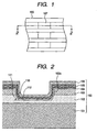
- FIG. 1 is a schematic plan view that shows the construction of a substrate for an ink jet recording head according to the present invention and, particularly, a plan view that shows the area near a heat acting portion 107 of a substrate for a head.
- FIG. 2 is a schematic sectional view of the section taken along the line 2-2 in FIG. 1 .
- a heat generating resistive layer 104 covers a pair of electrodes in an electrode layer 103 formed on an insulative lower layer 102, which is formed on a surface of a board 101 and serves as heat accumulation layer 102, and in the lower layer 102 there is formed a recess in a position corresponding to a section between the pair of electrodes.
- the heat generating resistive layer 104 is bent in rough U shape within the recess formed in the section of the lower layer 102 between the pair of electrodes in the electrode layer 103.
- the portion of the heat generating resistive layer 104 to which thermal stresses due to current concentration are applied most strongly i.e., the portion of the heat generating resistive layer 104 which covers a boundary 110 between an end portion (a stepped portion) 103a of the electrode layer 103 and the lower layer 102 is away from a bent portion 112 where the film quality of the heat generating resistive layer 104 is relatively poor, and hence it is possible to suppress the occurrence of broken wires of the heat generating resistive layer 104 caused by thermal stresses generated in the heat generating resistive layer 104.
- the bend angle in a roughly U-shaped bent portion 112 of the heat generating resistive layer 104 positioned between the pair of electrodes in the electrode layer 103 becomes gentler. Therefore, the film quality of the heat generating resistive layer 104 in the surface portion can be made better and the discharge endurance can be improved.
- the structure of the bent portion 112 can be formed gentler, whereby the occurrence of broken wires of the heat generating resistive layer 104 due to thermal stresses generated in the heat generating resistive layer 104 is further suppressed and the discharge endurance can be further improved.
- the shape of the bent portion 113 of the protective layer becomes gentler than the shape of the structure of FIG. 2 and the step coverage of protective layers 105, 106 becomes better than the step coverage of the structure of FIG. 2 .
- the film thickness of the upper insulative protective layer 105 is further reduced and a liquid such as ink can be discharged by ensuring bubbling with less power.
- a heat generating resistive layer 104 at a boundary 110 between the portion covering the tapered portion of the lower layer 102 and the portion covering the top of the end portion of the electrode layer 103 which is continuous with the surface portion can be made gentler than in the structure of FIG. 2 .
- the film quality of the surface portion of the heat generating resistive layer 104 can be improved, the occurrence of broken wires due to thermal stresses can be further suppressed and the discharge durability can be further improved.
- the smaller the taper angle 111 in the lower layer 102 the more the film quality of the surface portion of the heat generating resistive layer 104 will be improved, and hence this is desirable.
- the smaller the taper angle 109 of the tapered portion in the end portion of the electrode layer 103 the lower the accuracy of the distance between the pair of electrodes in the electrode layer 103, and the more variations in the electrical properties as a heat generating portion 107 will be apt to occur. Therefore, it is necessary to pay attention to this point.
- the step coverage of the upper insulative protective layer 105 and upper metal protective layer 106 that cover a heat generating resistive layer 104 is further improved. For this reason, it is possible to make the film thickness of the upper insulative protective layer 105 and upper metal protective layer 106 smaller than in the case of the structures of FIGS. 2 and 3 without impairing the discharge endurance performance. As a result of this, power can be saved when the heat from a heat generating portion is transmitted to ink.
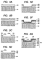
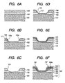
- FIGS. 5A, 5B, 5C, 5D, 5E, 5F, 5G , 6A, 6B, 6C, 6D, 6E and 6F sequentially explain the manufacturing process of the structure shown in FIGS. 2 , 6A, 6B, 6C, 6D, 6E and 6F sequentially explain the manufacturing process of the structures shown in FIGS. 3 and 4 by using the section taken along the line 2-2 of FIG. 1 .
- FIGS. 5A, 5B, 5C, 5D, 5E, 5F and 5G An SiO 2 layer which becomes a lower layer 102 serving as a heat accumulation layer 102 was formed on a silicon board 101 in a thickness of 1.0 ⁇ m by the thermal oxidation method ( FIG. 5A ) and Al was formed as an electrode layer 103 on the lower layer 102 in a thickness of 0.6 ⁇ m by the sputtering method ( FIG. 5B ). And a resist was patterned in a desired shape on the electrode layer 103 by the photolithography method and the electrode layer 103 was etched by dry etching, whereby the electrode layer 103 having a desired wiring configuration was obtained ( FIG. 5C ).
- This etching was performed by use of an ECR etching device.
- the gas pressure was 2.66 Pa
- Cl 2 /BCI 2 gas was used
- the microwave power was 100 W.
- Etching was performed so that a patterning end portion 103a of the electrode layer 103 became substantially perpendicular to the substrate as shown in FIG. 5C in an etching time of a little less than about 50 seconds.
- a somewhat high vacuum of 1.33 Pa is achieved by lowering the gas pressure, the lower layer 102 which becomes exposed due to the etching of the electrode layer 103 begins to be etched in concave shape.
- the electrode layer 103 is etched mainly by chemical drying
- the lower layer 102 for which etching is performed in an atmosphere of higher vacuum, is etched mainly by sputter etching.
- the end portion of the lower layer 102 which is continuous from the end portion 103a of the electrode layer 103 was etched in such a manner as to provide a tapered inclined surface having a certain angle ( FIG. 5D ).
- a TaN film was formed as a heat generating resistive layer 104 on the patterned electrode layer 103 in a thickness of 0.04 ⁇ m by the sputtering method ( FIG. 5E ).
- a resist was patterned in a desired shape by the photolithography method and a heat generating portion 107 was formed by the dry etching method or the wet etching method.
- an SiN film was formed from ink in a thickness of 0.3 ⁇ m by the plasma CVD method as an upper insulative protective film 105 to protect the electrode layer 103 and the heat generating resistive layer 104 ( FIG. 5F ).
- a Ta film was formed as a metal protective layer 106 in a thickness of 0.2 ⁇ m.
- the protective layer may a single layer of a single material or as described above, it may have a laminated structure of an insulative layer 105 of, for example, Si 3 N 4 , SiO 2 SiON, Ta 2 O 5 , etc. and a metal layer 106 of Ta etc. to improve cavitation resistance.
- a substrate for an ink jet recording head having the heat generating portion 107 was thus formed.
- FIG. 6A corresponds to FIG. 5B .
- a resist was patterned in a desired shape by the photolithography method and the electrode layer 103 and the lower layer 102 were etched by the dry etch method. This etching was performed by use of an ECR etching device.
- the etching conditions were such that the gas pressure was 1.33 Pa, Cl 2 /BCI 2 gas was used, and the microwave power was 100 W (in the steps shown in FIGS. 5A, 5B, 5C, 5D, 5E, 5F and 5G , the same as the dry etching conditions shown in FIG. 5D and following figures). It took 120 seconds to etch the electrode layer 103 required, and it took 70 seconds to etch the lower layer 102. As described above, the end portions of the two layers were etched mainly by sputter etching rather than by chemical dry etching.
- the tapered shape varied further and the taper angle became smaller ( FIG. 6B ).
- the lower layer 102 had a taper angle 111 of 60 degrees and the electrode layer 103 had a taper angle 109 of 70 degrees.
- the two taper angles may be caused to differ from each other by adopting different etching conditions for the electrode layer 103 and the heat accumulation layer 104, which is the base of the electrode layer 103.
- the etching conditions may be changed so that the taper angle 109 of the end portion of the electrode layer 103 is changed as to be reduced by stages.
- a TaN film having a film thickness of 0.04 ⁇ m as a heat generating resistive layer 104 and an SiN film having a film thickness of 0.3 ⁇ m as an upper insulative protective film 105 were formed on the electrode layer 103, and a Ta film having a film thickness of 0.2 ⁇ m as a metal protective film 106 was further formed on the upper insulative protective film 105, whereby a substrate for an ink jet recording head having a heat generating resistive body of the structure shown in FIG. 3 was formed.
- a TaN film having a film thickness of 0.04 ⁇ m as a heat generating resistive layer 104 ( FIG. 6D )and an SiN film having a film thickness of 0.3 ⁇ m as an upper insulative protective film 105 ( FIG. 6E ) were formed on the electrode layer 103, and a Ta film having a film thickness of 0.2 ⁇ m as a metal protective film 106 ( FIG. 6F ) was further formed on the upper insulative protective film 105, whereby a substrate for an ink jet recording head having a heat generating resistive body of the structure shown in FIG. 4 was formed.
- the corner portion of the electrode layer has no area having an acute angle.
- the corner portion of the electrode layer has roundness even if only slightly, it is possible to obtain an effect according to the degree of the roundness.
- FIG. 7 is a schematic perspective view of a top board having liquid channels and grooves for the formation of a liquid chamber, which constitutes an ink jet recording head manufactured obtained by using a substrate for a head manufactured by the above-described manufacturing method
- FIG. 8 is a schematic perspective view of an ink jet recording head, which is assembled by using a substrate for a head manufactured by the above-described manufacturing method and the top board of FIG. 7 .
- the ink jet recording head shown in FIG. 8 is obtained by joining to this substrate 100 a top board 16 ( FIG. 7 ) having liquid channels 17 corresponding to each of the thermal energy generating means and grooves 18 formed to provide liquid discharge ports 21 in communication with the liquid channels.
- a liquid supply tube 20 is connected to a common liquid chamber 19 as required, and a liquid such as ink is introduced into the head through the liquid supply tube 20.
- Electrodes 11, 12 supply the energy power for ink discharge to the heat acting portion (heat generating portion) 107 by conducting with each of the above-described pair of electrode layers.
- the use of the top board 16 is not always necessary and these components may be formed by the patterning of a photosensitive resin and the like.
- the present invention is not limited only to a multiarray type ink jet recording head having multiple liquid discharge outlets as described above, and of course it can be applied also to a single-array type ink jet recording head having one liquid discharge outlet.
- a discharge endurance test of ink was conducted by using this head.
- the heat generating resistive layer 104 showed no broken wire even after the input of discharge signals of not less than 1 X 10 9 pulses although the film thickness of the upper insulative protective layer 105 was 1/2 of the film thickness of the electrode layer 103, and the pulse endurance life was longer than that of a head of the conventional structure shown in FIG. 10 .
- the portion of the heat generating resistive layer 104 to which thermal stresses by the current concentration are applied most strongly i.e., the portion of the heat generating resistive layer 104 which covers a boundary (a stepped portion of the electrode layer) 110 between an end portion of the electrode layer 103 and the heat accumulation layer 102) is away from a bent portion 112 where the film quality of the heat generating resistive layer 104 is relatively poor, and because by ensuring that the angle 109 of the tapered shape (the taper angle of the electrode layer) in the end portion of the pair of electrode layers is larger than the taper angle 111 (the taper angle of the base) in the tapered portion of the lower layer 102, which is a support of the base of the electrode layer, the heat generating resistive layer 104 covering the boundary 110 between the end portion of the electrode layer 103 and the tapered portion of the lower layer 102, the film quality of the surface portion of the heat generating resistive layer 104 can be improved. As a result of this, the portion of the heat generating resistive layer
- the shape of the bent portion 113 of the protective layers 105, 106 becomes gentler. Besides the step coverage of the protective layers 105, 106 is improved by rounding the corner portion 114 of the electrode layer 103 and the heat generated in the heat acting portion 107 is efficiently transmitted to a liquid such as ink by further reducing the film thickness of the upper insulative protective layer 105. Therefore, the liquid can be discharged by causing bubbling with less power.
Landscapes
- Engineering & Computer Science (AREA)
- Manufacturing & Machinery (AREA)
- Particle Formation And Scattering Control In Inkjet Printers (AREA)
Applications Claiming Priority (4)
| Application Number | Priority Date | Filing Date | Title |
|---|---|---|---|
| JP2004137510 | 2004-05-06 | ||
| JP2004137510 | 2004-05-06 | ||
| JP2005106287A JP4537246B2 (ja) | 2004-05-06 | 2005-04-01 | インクジェット記録ヘッド用基体の製造方法及び該方法により製造された前記基体を用いた記録ヘッドの製造方法 |
| JP2005106287 | 2005-04-01 |
Publications (3)
| Publication Number | Publication Date |
|---|---|
| EP1593515A2 EP1593515A2 (en) | 2005-11-09 |
| EP1593515A3 EP1593515A3 (en) | 2006-09-06 |
| EP1593515B1 true EP1593515B1 (en) | 2010-12-15 |
Family
ID=34935955
Family Applications (1)
| Application Number | Title | Priority Date | Filing Date |
|---|---|---|---|
| EP05009443A Not-in-force EP1593515B1 (en) | 2004-05-06 | 2005-04-29 | Method of manufacturing substrate for ink jet recording head and method of manufacturing recording head using substrate manufactured by this method |
Country Status (6)
| Country | Link |
|---|---|
| US (1) | US7452474B2 (ja) |
| EP (1) | EP1593515B1 (ja) |
| JP (1) | JP4537246B2 (ja) |
| KR (1) | KR100846348B1 (ja) |
| DE (1) | DE602005025276D1 (ja) |
| TW (1) | TWI274667B (ja) |
Families Citing this family (18)
| Publication number | Priority date | Publication date | Assignee | Title |
|---|---|---|---|---|
| JP4522086B2 (ja) * | 2003-12-15 | 2010-08-11 | キヤノン株式会社 | 梁、梁の製造方法、梁を備えたインクジェット記録ヘッド、および該インクジェット記録ヘッドの製造方法 |
| EP1768848B1 (en) * | 2004-06-28 | 2010-07-21 | Canon Kabushiki Kaisha | Liquid discharge head manufacturing method, and liquid discharge head obtained using this method |
| DE602005015974D1 (de) * | 2004-06-28 | 2009-09-24 | Canon Kk | Kopfs und unter verwendung dieses verfahrens erhaltener flüssigkeitsabgabekopf |
| JP4137027B2 (ja) * | 2004-08-16 | 2008-08-20 | キヤノン株式会社 | インクジェットヘッド用基板、該基板の製造方法および前記基板を用いるインクジェットヘッド |
| JP4182035B2 (ja) * | 2004-08-16 | 2008-11-19 | キヤノン株式会社 | インクジェットヘッド用基板、該基板の製造方法および前記基板を用いるインクジェットヘッド |
| JP2006130868A (ja) * | 2004-11-09 | 2006-05-25 | Canon Inc | インクジェット記録ヘッド及びその製造方法 |
| JP2006137030A (ja) * | 2004-11-10 | 2006-06-01 | Canon Inc | 液体吐出記録ヘッド及びその製造方法 |
| JP4641440B2 (ja) * | 2005-03-23 | 2011-03-02 | キヤノン株式会社 | インクジェット記録ヘッドおよび該インクジェット記録ヘッドの製造方法 |
| JP4766658B2 (ja) * | 2005-05-10 | 2011-09-07 | キヤノン株式会社 | 液体吐出ヘッドおよびその製造方法 |
| US7637013B2 (en) * | 2005-08-23 | 2009-12-29 | Canon Kabushiki Kaisha | Method of manufacturing ink jet recording head |
| US8438729B2 (en) * | 2006-03-09 | 2013-05-14 | Canon Kabushiki Kaisha | Method of producing liquid discharge head |
| KR20080000421A (ko) * | 2006-06-27 | 2008-01-02 | 삼성전자주식회사 | 프린트 헤드 및 그 제조방법 |
| JP4981491B2 (ja) * | 2007-03-15 | 2012-07-18 | キヤノン株式会社 | インクジェットヘッド製造方法及び貫通電極の製造方法 |
| JP5361231B2 (ja) * | 2008-03-26 | 2013-12-04 | キヤノン株式会社 | インクジェット記録ヘッド及び電子デバイス |
| JP4656670B2 (ja) * | 2008-12-19 | 2011-03-23 | キヤノン株式会社 | 液体吐出ヘッド及び液体吐出ヘッドの製造方法 |
| US8012773B2 (en) * | 2009-06-11 | 2011-09-06 | Canon Kabushiki Kaisha | Method for manufacturing liquid discharge head |
| US8499453B2 (en) * | 2009-11-26 | 2013-08-06 | Canon Kabushiki Kaisha | Method of manufacturing liquid discharge head, and method of manufacturing discharge port member |
| US8434229B2 (en) * | 2010-11-24 | 2013-05-07 | Canon Kabushiki Kaisha | Liquid ejection head manufacturing method |
Family Cites Families (23)
| Publication number | Priority date | Publication date | Assignee | Title |
|---|---|---|---|---|
| US647769A (en) * | 1899-07-10 | 1900-04-17 | David Strawbridge | Condiment-holder. |
| JPS60159062A (ja) | 1984-01-31 | 1985-08-20 | Canon Inc | 液体噴射記録ヘツド |
| ATE144193T1 (de) * | 1990-12-12 | 1996-11-15 | Canon Kk | Tintenstrahlaufzeichnung |
| JPH06188108A (ja) * | 1992-12-21 | 1994-07-08 | Canon Inc | 薄膜抵抗器の製造方法、成膜装置用防着板及び成膜装置 |
| US5636441A (en) * | 1995-03-16 | 1997-06-10 | Hewlett-Packard Company | Method of forming a heating element for a printhead |
| JPH0911468A (ja) * | 1995-06-29 | 1997-01-14 | Canon Inc | インクジェット記録ヘッド用基体、インクジェット記録ヘッド、インクジェット記録装置および情報処理システム |
| JPH11227210A (ja) * | 1997-12-05 | 1999-08-24 | Canon Inc | 液体吐出ヘッド、該ヘッドの製造方法、ヘッドカートリッジおよび液体吐出装置 |
| JP2000198199A (ja) * | 1997-12-05 | 2000-07-18 | Canon Inc | 液体吐出ヘッドおよびヘッドカートリッジおよび液体吐出装置および液体吐出ヘッドの製造方法 |
| US6142606A (en) * | 1997-12-22 | 2000-11-07 | Canon Kabushiki Kaisha | Ink jet recording head, substrate for use of such head, ink jet cartridge, and ink jet recording apparatus |
| JP2000177135A (ja) | 1998-10-08 | 2000-06-27 | Canon Inc | インクジェット記録ヘッド用基板、インクジェット記録ヘッドおよびその製造方法 |
| US6357862B1 (en) * | 1998-10-08 | 2002-03-19 | Canon Kabushiki Kaisha | Substrate for ink jet recording head, ink jet recording head and method of manufacture therefor |
| EP1000745A3 (en) * | 1998-10-27 | 2001-01-24 | Canon Kabushiki Kaisha | Electro-thermal conversion device board, ink-jet recording head provided with the electro-thermal conversion device board, ink-jet recording apparatus using the same, and production method of ink-jet recording head |
| JP3592136B2 (ja) * | 1999-06-04 | 2004-11-24 | キヤノン株式会社 | 液体吐出ヘッドおよびその製造方法と微小電気機械装置の製造方法 |
| US6474769B1 (en) | 1999-06-04 | 2002-11-05 | Canon Kabushiki Kaisha | Liquid discharge head, liquid discharge apparatus and method for manufacturing liquid discharge head |
| US6402302B1 (en) * | 1999-06-04 | 2002-06-11 | Canon Kabushiki Kaisha | Liquid discharge head, manufacturing method thereof, and microelectromechanical device |
| JP3647365B2 (ja) * | 1999-08-24 | 2005-05-11 | キヤノン株式会社 | 液体吐出ヘッド用基板ユニットおよびその製造方法ならびに液体吐出ヘッド,カートリッジおよび画像形成装置 |
| JP3652185B2 (ja) * | 1999-10-05 | 2005-05-25 | キヤノン株式会社 | 液体吐出装置 |
| JP2001105599A (ja) * | 1999-10-05 | 2001-04-17 | Canon Inc | 液体吐出ヘッド、液体吐出ヘッドの製造方法および液体吐出装置 |
| KR20020025588A (ko) * | 2000-09-29 | 2002-04-04 | 윤종용 | 잉크젯 프린터 헤드 |
| JP3970119B2 (ja) * | 2002-07-19 | 2007-09-05 | キヤノン株式会社 | インクジェット記録ヘッドおよび該インクジェット記録ヘッドを用いた記録装置 |
| JP2005125494A (ja) * | 2003-10-21 | 2005-05-19 | Fuji Xerox Co Ltd | インクジェット記録ヘッド及びインクジェット記録ヘッドの製造方法、並びにインクジェット記録装置。 |
| JP4182035B2 (ja) * | 2004-08-16 | 2008-11-19 | キヤノン株式会社 | インクジェットヘッド用基板、該基板の製造方法および前記基板を用いるインクジェットヘッド |
| JP4137027B2 (ja) * | 2004-08-16 | 2008-08-20 | キヤノン株式会社 | インクジェットヘッド用基板、該基板の製造方法および前記基板を用いるインクジェットヘッド |
-
2005
- 2005-04-01 JP JP2005106287A patent/JP4537246B2/ja not_active Expired - Fee Related
- 2005-04-25 TW TW094113137A patent/TWI274667B/zh not_active IP Right Cessation
- 2005-04-29 DE DE602005025276T patent/DE602005025276D1/de active Active
- 2005-04-29 EP EP05009443A patent/EP1593515B1/en not_active Not-in-force
- 2005-05-02 US US11/118,404 patent/US7452474B2/en active Active
- 2005-05-04 KR KR1020050037551A patent/KR100846348B1/ko not_active IP Right Cessation
Also Published As
| Publication number | Publication date |
|---|---|
| TW200606023A (en) | 2006-02-16 |
| EP1593515A3 (en) | 2006-09-06 |
| KR20060045903A (ko) | 2006-05-17 |
| DE602005025276D1 (de) | 2011-01-27 |
| KR100846348B1 (ko) | 2008-07-15 |
| JP4537246B2 (ja) | 2010-09-01 |
| EP1593515A2 (en) | 2005-11-09 |
| JP2005343171A (ja) | 2005-12-15 |
| TWI274667B (en) | 2007-03-01 |
| US7452474B2 (en) | 2008-11-18 |
| US20050248623A1 (en) | 2005-11-10 |
Similar Documents
| Publication | Publication Date | Title |
|---|---|---|
| EP1593515B1 (en) | Method of manufacturing substrate for ink jet recording head and method of manufacturing recording head using substrate manufactured by this method | |
| EP1177899B1 (en) | Ink jet head with anti-cavitation film preventing kogation and erosion | |
| EP0768182B1 (en) | A method for manufacturing an ink jet recording head, an ink jet recording head manufactured by such method, and an ink jet recording apparatus having such ink jet recording head mounted thereon | |
| US11001062B2 (en) | Liquid ejection head and a manufacturing method of the same | |
| KR100560593B1 (ko) | 액체 토출 헤드의 제조방법 | |
| KR20030040689A (ko) | 잉크젯 프린트헤드 및 그 제조방법 | |
| CN100588547C (zh) | 喷墨记录头用基体的制造方法和记录头的制造方法 | |
| JP2004358971A (ja) | 一体型インクジェットプリントヘッドおよびその製造方法 | |
| US6818138B2 (en) | Slotted substrate and slotting process | |
| US7473649B2 (en) | Methods for controlling feature dimensions in crystalline substrates | |
| AU2004282922A1 (en) | Thin film ink jet printhead adhesion enhancement | |
| EP1491341A2 (en) | Thermally-driven ink-jet printhead without cavitation damage of heater | |
| JP5038054B2 (ja) | 液体吐出ヘッドおよびその製造方法 | |
| JPH08112902A (ja) | インクジェットヘッド用基板、インクジェットヘッド及びインクジェット装置の製造方法並びにインクジェットヘッド用基板、インクジェットヘッド及びインクジェット装置 | |
| US10166772B2 (en) | Liquid-discharging-head substrate, liquid discharging head, liquid discharging apparatus, method of manufacturing liquid-discharging-head substrate | |
| JP2005280179A (ja) | インクジェットヘッド用基板およびインクジェットヘッド | |
| JP2003136738A (ja) | 回路基板及び液体吐出ヘッド、並びにそれらの製造方法 | |
| JP2007245639A (ja) | インクジェット記録ヘッドの製造方法 | |
| JP4731892B2 (ja) | 液体吐出ヘッド用の半導体基板の供給口および貫通口の製造方法 | |
| US9597874B2 (en) | Liquid ejection head, liquid ejecting apparatus, and method for manufacturing liquid ejection head | |
| KR100400228B1 (ko) | 잉크젯 프린트헤드 및 그 제조방법 | |
| JP2006225745A (ja) | 薄膜素子の構造および製造方法 | |
| JPH0957970A (ja) | 液体噴射記録ヘッド用基体及びその製造方法 | |
| JP2007283669A (ja) | インクジェット記録ヘッド、インクジェット記録ヘッドの製造方法 | |
| JPH04241950A (ja) | サーマルインクジェットヘッド |
Legal Events
| Date | Code | Title | Description |
|---|---|---|---|
| PUAI | Public reference made under article 153(3) epc to a published international application that has entered the european phase |
Free format text: ORIGINAL CODE: 0009012 |
|
| AK | Designated contracting states |
Kind code of ref document: A2 Designated state(s): AT BE BG CH CY CZ DE DK EE ES FI FR GB GR HU IE IS IT LI LT LU MC NL PL PT RO SE SI SK TR |
|
| AX | Request for extension of the european patent |
Extension state: AL BA HR LV MK YU |
|
| PUAL | Search report despatched |
Free format text: ORIGINAL CODE: 0009013 |
|
| AK | Designated contracting states |
Kind code of ref document: A3 Designated state(s): AT BE BG CH CY CZ DE DK EE ES FI FR GB GR HU IE IS IT LI LT LU MC NL PL PT RO SE SI SK TR |
|
| AX | Request for extension of the european patent |
Extension state: AL BA HR LV MK YU |
|
| RIC1 | Information provided on ipc code assigned before grant |
Ipc: B41J 2/16 20060101AFI20050818BHEP Ipc: B41J 2/14 20060101ALI20060801BHEP |
|
| 17P | Request for examination filed |
Effective date: 20070306 |
|
| AKX | Designation fees paid |
Designated state(s): DE FR GB IT |
|
| 17Q | First examination report despatched |
Effective date: 20070419 |
|
| GRAP | Despatch of communication of intention to grant a patent |
Free format text: ORIGINAL CODE: EPIDOSNIGR1 |
|
| GRAS | Grant fee paid |
Free format text: ORIGINAL CODE: EPIDOSNIGR3 |
|
| GRAA | (expected) grant |
Free format text: ORIGINAL CODE: 0009210 |
|
| AK | Designated contracting states |
Kind code of ref document: B1 Designated state(s): DE FR GB IT |
|
| REG | Reference to a national code |
Ref country code: GB Ref legal event code: FG4D |
|
| REF | Corresponds to: |
Ref document number: 602005025276 Country of ref document: DE Date of ref document: 20110127 Kind code of ref document: P |
|
| PLBE | No opposition filed within time limit |
Free format text: ORIGINAL CODE: 0009261 |
|
| STAA | Information on the status of an ep patent application or granted ep patent |
Free format text: STATUS: NO OPPOSITION FILED WITHIN TIME LIMIT |
|
| 26N | No opposition filed |
Effective date: 20110916 |
|
| REG | Reference to a national code |
Ref country code: DE Ref legal event code: R097 Ref document number: 602005025276 Country of ref document: DE Effective date: 20110916 |
|
| PGFP | Annual fee paid to national office [announced via postgrant information from national office to epo] |
Ref country code: FR Payment date: 20140428 Year of fee payment: 10 Ref country code: IT Payment date: 20140402 Year of fee payment: 10 |
|
| PG25 | Lapsed in a contracting state [announced via postgrant information from national office to epo] |
Ref country code: IT Free format text: LAPSE BECAUSE OF NON-PAYMENT OF DUE FEES Effective date: 20150429 |
|
| REG | Reference to a national code |
Ref country code: FR Ref legal event code: ST Effective date: 20151231 |
|
| PG25 | Lapsed in a contracting state [announced via postgrant information from national office to epo] |
Ref country code: FR Free format text: LAPSE BECAUSE OF NON-PAYMENT OF DUE FEES Effective date: 20150430 |
|
| PGFP | Annual fee paid to national office [announced via postgrant information from national office to epo] |
Ref country code: GB Payment date: 20170420 Year of fee payment: 13 Ref country code: DE Payment date: 20170430 Year of fee payment: 13 |
|
| REG | Reference to a national code |
Ref country code: DE Ref legal event code: R119 Ref document number: 602005025276 Country of ref document: DE |
|
| GBPC | Gb: european patent ceased through non-payment of renewal fee |
Effective date: 20180429 |
|
| PG25 | Lapsed in a contracting state [announced via postgrant information from national office to epo] |
Ref country code: DE Free format text: LAPSE BECAUSE OF NON-PAYMENT OF DUE FEES Effective date: 20181101 |
|
| PG25 | Lapsed in a contracting state [announced via postgrant information from national office to epo] |
Ref country code: GB Free format text: LAPSE BECAUSE OF NON-PAYMENT OF DUE FEES Effective date: 20180429 |