EP1577978A1 - Leiterplattenverbindungsanschluss - Google Patents
Leiterplattenverbindungsanschluss Download PDFInfo
- Publication number
- EP1577978A1 EP1577978A1 EP03777218A EP03777218A EP1577978A1 EP 1577978 A1 EP1577978 A1 EP 1577978A1 EP 03777218 A EP03777218 A EP 03777218A EP 03777218 A EP03777218 A EP 03777218A EP 1577978 A1 EP1577978 A1 EP 1577978A1
- Authority
- EP
- European Patent Office
- Prior art keywords
- circuit board
- connecting portion
- board connector
- connector according
- cut surfaces
- Prior art date
- Legal status (The legal status is an assumption and is not a legal conclusion. Google has not performed a legal analysis and makes no representation as to the accuracy of the status listed.)
- Withdrawn
Links
Images




Classifications
-
- H—ELECTRICITY
- H01—ELECTRIC ELEMENTS
- H01R—ELECTRICALLY-CONDUCTIVE CONNECTIONS; STRUCTURAL ASSOCIATIONS OF A PLURALITY OF MUTUALLY-INSULATED ELECTRICAL CONNECTING ELEMENTS; COUPLING DEVICES; CURRENT COLLECTORS
- H01R43/00—Apparatus or processes specially adapted for manufacturing, assembling, maintaining, or repairing of line connectors or current collectors or for joining electric conductors
- H01R43/16—Apparatus or processes specially adapted for manufacturing, assembling, maintaining, or repairing of line connectors or current collectors or for joining electric conductors for manufacturing contact members, e.g. by punching and by bending
Definitions
- the present invention relates to circuit board connectors for connecting two circuit boards together.
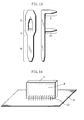
- This circuit board connector comprises, as illustrated in Fig. 13, a main body portion 2, a first connecting portion 1 for connection to a first circuit board, a second circuit board connection 4 for connection to a second circuit board, and a lead portion 3 located between the second connecting portion 4 and the main body portion 2.
- the main body portion 2 comprises an auxiliary connecting portion 21 formed from a portion of the main body portion 2, so that the connecting strength is improved by making connection with the first circuit board at two points, at the first connecting portion 1 and the auxiliary connecting portion 21.
- an electronic device 7 such as a tuner is arranged uprightly in order to reduce the mounting area of the circuit board.
- This necessitates the second connecting portion 4 to be drawn out from a narrow surface of the circuit board that is arranged, in the electronic device, parallel to a wide surface in the electronic apparatus, and therefore, the first connecting portion 1 and the auxiliary connecting portion 21 are bent when connected to a circuit board within the electronic device.
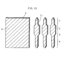
- the outer shape of the above-described circuit board connector is, as illustrated in Fig. 15, formed by press cutting a single sheet of conductive plate material 5 the front and back sides of which have plating layers 6 of tin, nickel, or the like that have been formed thereon in advance.
- the transverse cross sections of the first connecting portion 1, the second connecting portion 4, and the auxiliary connecting portion 21 are formed to be rectangular.
- cut surfaces 11 created by the press cutting are not provided with the plating layers and therefore have lower solder wettability than those in which a plating layer is formed on the entire surfaces.
- there is a certain length of time until an electronic device equipped with the circuit board connector is shipped to the user and mounted onto a circuit board of an electronic apparatus. During that time, the second connecting portion of the circuit board connector is oxidized or rusted, and consequently a problem arises that solder wettability reduces.
- Re-plating the terminal adds an extra manufacturing step and also increases cost.
- the re-plating process usually adopts a barrel plating method, which involves putting samples to be plated into a barrel-shaped container containing a plating solution and revolving the barrel-shaped container, and in the course of this process, the terminals deform or get tangled, reducing the yield and leading to a further increase in cost.
- a thin conductive plate material is used for cost reduction, the mechanical strength of the circuit board connector degrades, resulting in breakage during the manufacturing process and the mounting process to a circuit board, which also reduces the manufacturing yield.
- the present invention has been accomplished to solve such problems, and it provides a circuit board connector with which good soldering is possible even without performing a re-plating process.
- a circuit board connector of the present invention comprises a main body portion, a first connecting portion for connection to a first circuit board, and a second connecting portion for connection to a second circuit board; and the circuit board connector is obtained by cutting a conductive plate material provided with plating layers on front and back sides thereof, and thereafter forming the second connecting portion so as to have an annular transverse cross section in such a manner that one of the plating layers forms an outer circumferential surface of the second connecting portion.
- cut surfaces at both edges of the second connecting portion oppose each other in addition to the foregoing configuration.
- a gap is provided between the cut surfaces at both edges of the second connecting portion that oppose each other.
- a circuit board connector of the present invention is such that a circuit board connector comprising a first connecting portion for connection to a first circuit board and a second connecting portion connected to a second circuit board, wherein: the circuit board connector is obtained by cutting a conductive plate material provided with plating layers on front and back sides, and thereafter forming the second connecting portion so as to have an annular transverse cross section and bending the second connecting portion so that cut surfaces are located inside the annular cross-sectional shape.
- solder wettability can be improved without performing an extra plating process.
- the mechanical strength of the circuit board connector can be improved, and therefore, a conductive plate material that is thinner than that in conventional products can be used; thereby, cost can be reduced.
- the cut surfaces at both edges of the second connecting portion oppose each other, the cut surfaces, which are not plated, are not present in the outer circumferential surface; thus, solder wettability can be improved.
- solder comes into the gap by capillary action, making it possible to improve solder wettability.
- the second connecting portion By forming the second connecting portion so as to have an annular transverse cross section and bending the second connecting portion so that the cut surfaces are located inside the annular shape, the cut surfaces that are not plated are kept away from the outer circumferential surface that is to be soldered. Therefore, rusting that develops on the cut surfaces over time does not easily reach the outer circumferential surface, making it possible to conduct good soldering.
- a circuit board connector comprises a main body portion 2, a first connecting portion 1 for connection to a first circuit board in an electronic device, a second circuit board connection 4 for connection to a second circuit board in an electronic apparatus, a lead portion 3 between the second connecting portion 4 and the main body portion 2, and an auxiliary connecting portion 21 formed from a part of the main body portion.
- the circuit board connector of the present invention is formed by cutting a conductive plate material provided with plating layers on its front and back sides, and thereafter forming the second connecting portion into a shape having an annular cross section so that one of the plating layers forms the outer circumferential surface of the second connecting portion.
- annular shape used in the present invention is intended to describe the shape that forms an inner hollow 16, and the outer shape is not particularly limited.
- annular cross-sectional shapes that may be adopted include, as illustrated in Fig. 12, a circular shape (a), an elliptical shape (b), and an elongated elliptical shape (c).
- the outer shape may be changed as appropriate depending on the shape of the terminal sockets of the second connecting circuit.
- plating layers used for the conductive plate material in the present invention there are no particular limitations on the plating layers used for the conductive plate material in the present invention as long as their materials have high electrical conductivity, and usable materials include gold, silver, copper, nickel, and palladium. In the following embodiments, a tin-plated conductive plate material was used.
- the circuit board connector according to the present invention is fabricated as follows. As illustrated in Fig. 1, the outer shape of the circuit board connector was formed by press-cutting a conductive plate material 13, which was a steel plate or the like the front and back sides of which are provided with tin plating layers, so that the interval (P) between the terminals was 4 mm.
- the cut surfaces 11 of the second connecting portion 4 were opposed so that one of the plating layers forms the outer circumferential surface of the second connecting portion, and thus the terminal was processed to have an annular cross section. Further, as illustrated in Fig. 4, the cut surfaces 11 of the lead portion 3 were opposed and the lead portion was processed to have an O-shaped transverse cross section, and thus, a circuit board connector as shown in Fig. 2 was completed.
- the second connecting portion 4 needed to be drawn out in a vertical direction from the circuit board arranged horizontally in the electronic device, the first connecting portion 1 and the auxiliary connecting portion 21 of the terminal were subjected to a bending process such as to be bent at right angles with respect to the second connecting portion.
- Fig. 5 is a front elevational view and a top view illustrating a second embodiment of the circuit board connector according to the present invention.
- the second circuit board connector was obtained as follows: the outer shape of the circuit board connector was formed using press-cutting as in the first embodiment; thereafter, as illustrated in Fig. 6, a gap was provided such that cut surfaces 11 at both edges of the second connecting portion do not come into close contact with each other and that it has a cross-sectional shape so that the plating layer forms the outer circumferential surface of the second connecting portion. Thereafter, the cut surface of the lead portion was processed into a C-shaped transverse cross section as illustrated in Fig. 7 for reinforcement, and thus a circuit board connector was completed.
- a circuit board connector of a third embodiment according to the present invention was obtained as follows.
- the outer shape was formed by press cutting a conductive plate material as in the first embodiment.
- the second connecting portion was processed as illustrated in Fig. 8 in the following manner. First, both ends of the second connecting portion near cut surfaces were bent at an acute angle, and thereafter, the second connecting portion was gradually processed through several manufacturing steps so as to have an annular cross section, so that the cut surfaces were brought inside the annular shape. Thereafter, the cut surface of the lead portion was processed into a C-shaped transverse cross section as illustrated in Fig. 7 for reinforcement, and thus a circuit board connector was completed.
- the first connecting portion 1 and the auxiliary connecting portion 21 are fixed onto the first circuit board by soldering and the second connecting portion 4 is fixed onto the second circuit board by soldering.
- the cut surfaces 11 of the conductive plate material 13 after the press-cutting are not present on the outer circumferential surface of the second connecting portion 4 of the terminal that is to be soldered, and therefore, solder wettability can be improved over conventional products.
- the terminal of the second embodiment is provided with a small gap between the cut surfaces 11 at both edges of the second connecting portion 4; therefore, solder comes into the gap by capillary action, making it possible to improve solder wettability.
- the terminal of the third embodiment has the cut surfaces 11 of the second connecting portion 4 that are bent so as to come inside the annular shape, making it possible to keep the cut surfaces 11 that are not plated away from the outer circumferential surface that is to be soldered. Consequently; even when rusting develops on the cut surfaces 11 over time and corrosion due to the rusting reaches the plated surface, the rust does not easily reach the outer circumferential surface of the second connecting portion, and therefore, it is possible to conduct good soldering. To obtain this effect, it is sufficient that the cut surfaces come inside the annular shape, and for example, the same effect can be attained with a shape as illustrated in Fig. 9, in which the cut surfaces of the portion to be soldered of the second connecting portion are processed to be rounded to come inside the annular shape.
- the gap between the portion to be soldered and the circular terminal connecting socket is not uniform, producing distant portions; therefore, the connecting strength is weak.
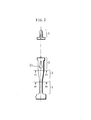
- the second connecting portion 4 of the terminal of the present invention is shaped to have an annular cross section, as illustrated in Fig. 10; therefore, the gap 15 to the circular terminal connecting socket 14 is uniform, making it possible to improve the connecting strength.
- the terminal in which the second connecting portion 4 is formed to have an annular transverse cross section as in the embodiments can improve the mechanical strength of the second connecting portion over the conventional product that is not subjected to a bending process. For this reason, it is possible to use a conductive material that is thinner than that in conventional products, leading to cost reduction. Furthermore, the mechanical strength of the terminal can be further improved by applying a bending process an O-shaped or C-shaped cross section or the like to the lead portion, as in the embodiments.
- the embodiments used one having an auxiliary connecting portion formed from a portion of the main body portion and the first connecting portion and the auxiliary connecting portion was bending-processed at right angles with respect to the second connecting portion; however, the number and shape of the first connecting portion(s) are not limited to the foregoing and may be varied within the scope of the claims.
- the first connecting portion of a terminal of the present invention as described above is used for an electronic device that is arranged uprightly, such as a tuner, it is possible to make effective use of the space on the circuit and to prevent occurrences of rusting and oxidation of the second connecting portion of the terminal. Consequently, good soldering can be conducted even when a certain time has elapsed after shipment of the electronic device until mounting of the electronic device onto an electronic apparatus.
- circuit board connector of the present invention good soldering is possible since a plating layer is formed on the outer circumferential surface of the second connecting portion. Moreover, it is possible to use a conductive plate material that is thinner than was conventionally possible because the mechanical strength of the second connecting portion is improved. Therefore, cost reduction can be achieved.
Landscapes
- Engineering & Computer Science (AREA)
- Manufacturing & Machinery (AREA)
- Coupling Device And Connection With Printed Circuit (AREA)
Applications Claiming Priority (3)
| Application Number | Priority Date | Filing Date | Title |
|---|---|---|---|
| JP2002350834 | 2002-12-03 | ||
| JP2002350834 | 2002-12-03 | ||
| PCT/JP2003/015497 WO2004051810A1 (ja) | 2002-12-03 | 2003-12-03 | 回路基板接続端子 |
Publications (2)
| Publication Number | Publication Date |
|---|---|
| EP1577978A1 true EP1577978A1 (de) | 2005-09-21 |
| EP1577978A4 EP1577978A4 (de) | 2007-08-22 |
Family
ID=32463122
Family Applications (1)
| Application Number | Title | Priority Date | Filing Date |
|---|---|---|---|
| EP03777218A Withdrawn EP1577978A4 (de) | 2002-12-03 | 2003-12-03 | Leiterplattenverbindungsanschluss |
Country Status (6)
| Country | Link |
|---|---|
| US (1) | US7235742B2 (de) |
| EP (1) | EP1577978A4 (de) |
| KR (1) | KR20050084093A (de) |
| CN (1) | CN1720644B (de) |
| AU (1) | AU2003289152A1 (de) |
| WO (1) | WO2004051810A1 (de) |
Families Citing this family (5)
| Publication number | Priority date | Publication date | Assignee | Title |
|---|---|---|---|---|
| KR20140027252A (ko) | 2011-04-12 | 2014-03-06 | 티코나 엘엘씨 | 송전 케이블용 복합체 코어 |
| TW201303192A (zh) | 2011-04-12 | 2013-01-16 | Ticona Llc | 用於水下應用之臍管 |
| KR20140015462A (ko) | 2011-04-12 | 2014-02-06 | 티코나 엘엘씨 | 연속 섬유 보강된 열가소성 봉 및 그를 제조하기 위한 인발 방법 |
| CN102290661B (zh) * | 2011-08-04 | 2013-03-13 | 苏州海创电子有限公司 | 卷圆端子及其制作方法 |
| CN207781937U (zh) * | 2018-01-04 | 2018-08-28 | 富士康(昆山)电脑接插件有限公司 | 电连接器端子 |
Family Cites Families (18)
| Publication number | Priority date | Publication date | Assignee | Title |
|---|---|---|---|---|
| US3764955A (en) * | 1972-05-17 | 1973-10-09 | Amp Inc | Connecting and mounting means for substrates |
| US3897992A (en) * | 1974-07-17 | 1975-08-05 | Amp Inc | Crimping connector means for fine wires |
| US4076356A (en) * | 1976-10-18 | 1978-02-28 | Bell Telephone Laboratories, Incorporated | Interconnection pin for multilayer printed circuit boards |
| US4150355A (en) * | 1978-01-04 | 1979-04-17 | Amp Incorporated | Electrical splices for wire wound resistors |
| JPS6328529Y2 (de) * | 1978-09-28 | 1988-08-01 | ||
| US4401352A (en) * | 1981-10-19 | 1983-08-30 | Amp Incorporated | Connector system for connecting a ceramic substrate to a printed circuit board |
| JPS6328529A (ja) | 1986-07-17 | 1988-02-06 | Mitsubishi Electric Corp | 産業用ロボツトを用いた組立部品構造 |
| US4867691A (en) * | 1987-10-29 | 1989-09-19 | E. I. Du Pont De Nemours And Company | Connector having expansible barrel with a layer of reflowable solder material thereon |
| JPH05121142A (ja) * | 1991-10-31 | 1993-05-18 | Yazaki Corp | 基板用端子の製造方法 |
| JPH05266936A (ja) | 1992-03-16 | 1993-10-15 | Matsushita Electric Ind Co Ltd | リードコムとプリント基板の接合構造 |
| JP3082453B2 (ja) | 1992-08-07 | 2000-08-28 | ダイキン工業株式会社 | 空気調和機 |
| JPH0658564U (ja) * | 1993-01-21 | 1994-08-12 | 沖電気工業株式会社 | プリント基板組み立て体 |
| US5980336A (en) * | 1995-06-09 | 1999-11-09 | Lear Automotive Dearborn, Inc. | Electrical terminal |
| JP4295384B2 (ja) * | 1999-03-08 | 2009-07-15 | 富士通コンポーネント株式会社 | コネクタ |
| JP2001043914A (ja) * | 1999-07-28 | 2001-02-16 | Sumitomo Wiring Syst Ltd | 基板用コネクタ |
| JP3831169B2 (ja) | 2000-01-25 | 2006-10-11 | 第一電子工業株式会社 | プレスインコンタクトの製造方法 |
| US6565367B2 (en) * | 2001-01-17 | 2003-05-20 | International Business Machines Corporation | Zero insertion force compliant pin contact and assembly |
| US6599145B2 (en) * | 2001-07-19 | 2003-07-29 | Visteon Global Technologies, Inc. | Twist lock connector system |
-
2003
- 2003-12-03 WO PCT/JP2003/015497 patent/WO2004051810A1/ja not_active Ceased
- 2003-12-03 CN CN2003801050614A patent/CN1720644B/zh not_active Expired - Fee Related
- 2003-12-03 EP EP03777218A patent/EP1577978A4/de not_active Withdrawn
- 2003-12-03 KR KR1020057009925A patent/KR20050084093A/ko not_active Ceased
- 2003-12-03 AU AU2003289152A patent/AU2003289152A1/en not_active Abandoned
- 2003-12-03 US US10/537,436 patent/US7235742B2/en not_active Expired - Fee Related
Also Published As
| Publication number | Publication date |
|---|---|
| KR20050084093A (ko) | 2005-08-26 |
| EP1577978A4 (de) | 2007-08-22 |
| US7235742B2 (en) | 2007-06-26 |
| US20060011373A1 (en) | 2006-01-19 |
| AU2003289152A1 (en) | 2004-06-23 |
| AU2003289152A8 (en) | 2004-06-23 |
| CN1720644A (zh) | 2006-01-11 |
| CN1720644B (zh) | 2010-04-14 |
| WO2004051810A1 (ja) | 2004-06-17 |
Similar Documents
| Publication | Publication Date | Title |
|---|---|---|
| US5944563A (en) | Press-in terminal for a connector | |
| US5641291A (en) | Printed circuit board connector | |
| US8070535B2 (en) | Printed circuit board terminal and printed circuit board connector having the same | |
| KR100884037B1 (ko) | 소형 안테나 및 그 제조방법 | |
| US4526436A (en) | Electrical connector for flat flexible cable | |
| JP2002343475A (ja) | Stmコネクタ及びその製造方法 | |
| US7235742B2 (en) | Circuit board connector | |
| EP0932221A2 (de) | Auf flexiblen Substrate montierte Kontaktstifte | |
| JP2000030834A (ja) | 基板用端子及びその製造方法 | |
| JP2003045231A (ja) | 制御器用ブスバー | |
| JPH065137U (ja) | 表面実装用電気コネクタに於ける端子 | |
| JP4346421B2 (ja) | 回路基板接続端子 | |
| EP1143577A2 (de) | Leitendes Element und zugehöriges Herstellungsverfahren | |
| JP3406257B2 (ja) | 表面実装用コネクタの製造方法 | |
| JP3155182B2 (ja) | 面実装型同軸コネクタ及び該面実装型同軸コネクタの製造方法 | |
| CN107591664A (zh) | 导电端子的制造方法 | |
| KR100304514B1 (ko) | 평평한가요성회로를사용하는전자장치및그제조방법 | |
| EP1429429A1 (de) | Verfahren zur Herstellung von Steckstiften und die Steckstifte selbst | |
| CN100388572C (zh) | 电连接器的盒式结构插孔接触件的局部电镀金方法 | |
| JP2736589B2 (ja) | コンタクト及びその製造方法 | |
| JP2005005481A (ja) | 可変抵抗器、及びその製造方法 | |
| CN222483923U (zh) | 玻璃电连接结构 | |
| JP3355470B2 (ja) | 金属端子の他の部材への固定構造及び固定方法 | |
| JPS60170181A (ja) | 電子部品用金属接片素子の製造方法の改良 | |
| CN114883888A (zh) | 一种导电端子制造工艺 |
Legal Events
| Date | Code | Title | Description |
|---|---|---|---|
| PUAI | Public reference made under article 153(3) epc to a published international application that has entered the european phase |
Free format text: ORIGINAL CODE: 0009012 |
|
| 17P | Request for examination filed |
Effective date: 20050627 |
|
| AK | Designated contracting states |
Kind code of ref document: A1 Designated state(s): AT BE BG CH CY CZ DE DK EE ES FI FR GB GR HU IE IT LI LU MC NL PT RO SE SI SK TR |
|
| AX | Request for extension of the european patent |
Extension state: AL LT LV MK |
|
| DAX | Request for extension of the european patent (deleted) | ||
| A4 | Supplementary search report drawn up and despatched |
Effective date: 20070724 |
|
| STAA | Information on the status of an ep patent application or granted ep patent |
Free format text: STATUS: THE APPLICATION HAS BEEN WITHDRAWN |
|
| 18W | Application withdrawn |
Effective date: 20101029 |