EP1577930A1 - Beschichtungsvorrichtung und herstellungsverfahren für beschichtungsfilm - Google Patents
Beschichtungsvorrichtung und herstellungsverfahren für beschichtungsfilm Download PDFInfo
- Publication number
- EP1577930A1 EP1577930A1 EP03780822A EP03780822A EP1577930A1 EP 1577930 A1 EP1577930 A1 EP 1577930A1 EP 03780822 A EP03780822 A EP 03780822A EP 03780822 A EP03780822 A EP 03780822A EP 1577930 A1 EP1577930 A1 EP 1577930A1
- Authority
- EP
- European Patent Office
- Prior art keywords
- substrate
- processed
- control member
- wafer
- airflow control
- Prior art date
- Legal status (The legal status is an assumption and is not a legal conclusion. Google has not performed a legal analysis and makes no representation as to the accuracy of the status listed.)
- Withdrawn
Links
Images


Classifications
-
- H—ELECTRICITY
- H10—SEMICONDUCTOR DEVICES; ELECTRIC SOLID-STATE DEVICES NOT OTHERWISE PROVIDED FOR
- H10P—GENERIC PROCESSES OR APPARATUS FOR THE MANUFACTURE OR TREATMENT OF DEVICES COVERED BY CLASS H10
- H10P72/00—Handling or holding of wafers, substrates or devices during manufacture or treatment thereof
- H10P72/04—Apparatus for manufacture or treatment
- H10P72/0448—Apparatus for applying a liquid, a resin, an ink or the like
-
- G—PHYSICS
- G03—PHOTOGRAPHY; CINEMATOGRAPHY; ANALOGOUS TECHNIQUES USING WAVES OTHER THAN OPTICAL WAVES; ELECTROGRAPHY; HOLOGRAPHY
- G03F—PHOTOMECHANICAL PRODUCTION OF TEXTURED OR PATTERNED SURFACES, e.g. FOR PRINTING, FOR PROCESSING OF SEMICONDUCTOR DEVICES; MATERIALS THEREFOR; ORIGINALS THEREFOR; APPARATUS SPECIALLY ADAPTED THEREFOR
- G03F7/00—Photomechanical, e.g. photolithographic, production of textured or patterned surfaces, e.g. printing surfaces; Materials therefor, e.g. comprising photoresists; Apparatus specially adapted therefor
- G03F7/16—Coating processes; Apparatus therefor
- G03F7/162—Coating on a rotating support, e.g. using a whirler or a spinner
-
- G—PHYSICS
- G03—PHOTOGRAPHY; CINEMATOGRAPHY; ANALOGOUS TECHNIQUES USING WAVES OTHER THAN OPTICAL WAVES; ELECTROGRAPHY; HOLOGRAPHY
- G03F—PHOTOMECHANICAL PRODUCTION OF TEXTURED OR PATTERNED SURFACES, e.g. FOR PRINTING, FOR PROCESSING OF SEMICONDUCTOR DEVICES; MATERIALS THEREFOR; ORIGINALS THEREFOR; APPARATUS SPECIALLY ADAPTED THEREFOR
- G03F7/00—Photomechanical, e.g. photolithographic, production of textured or patterned surfaces, e.g. printing surfaces; Materials therefor, e.g. comprising photoresists; Apparatus specially adapted therefor
- G03F7/70—Microphotolithographic exposure; Apparatus therefor
- G03F7/70691—Handling of masks or workpieces
- G03F7/707—Chucks, e.g. chucking or un-chucking operations or structural details
-
- H—ELECTRICITY
- H10—SEMICONDUCTOR DEVICES; ELECTRIC SOLID-STATE DEVICES NOT OTHERWISE PROVIDED FOR
- H10P—GENERIC PROCESSES OR APPARATUS FOR THE MANUFACTURE OR TREATMENT OF DEVICES COVERED BY CLASS H10
- H10P72/00—Handling or holding of wafers, substrates or devices during manufacture or treatment thereof
- H10P72/04—Apparatus for manufacture or treatment
- H10P72/0402—Apparatus for fluid treatment
Definitions
- the present invention relates to a coating process apparatus and a coating film forming method for forming a film by applying a coating liquid to a substrate to be processed.
- a predetermined circuit pattern is formed on a semiconductor wafer by using the photolithography technology.
- a resist film is formed on a wafer, the resist film is exposed in a predetermined pattern, and then the exposed wafer is developed, whereby the circuit pattern is formed thereon.
- spin coating As a method of forming a resist film on a wafer, so-called spin coating is widely used, which supplies a predetermined amount of a resist liquid is supplied to the center portion of a wafer held substantially horizontally and then rotates the wafer at a high speed so as to spread the resist liquid over the entire wafer surface.
- Unexamined Japanese Patent Application KOKAI Publication No. 2001-189266 discloses, as an apparatus which forms a film by such spin coating, a coating process apparatus which comprises a process cup so laid out as to surround a wafer and coercively exhausts the atmosphere around the wafer by carrying out coercive exhausting from the bottom, and an airflow control plate which is so provided as to surround the wafer in atmosphere around the wafer by carrying out coercive exhausting from the bottom, and an airflow control plate which is so provided as to surround the wafer in the process cup and controls an airflow generated around the wafer.
- a coating process apparatus which comprises a process cup so laid out as to surround a wafer and coercively exhausts the atmosphere around the wafer by carrying out coercive exhausting from the bottom, and an airflow control plate which is so provided as to surround the wafer in atmosphere around the wafer by carrying out coercive exhausting from the bottom, and an airflow control plate which is so provided as to surround the wafer in the process cup and controls an
- the present invention has been made in consideration of the situations, and it is an object of the present invention to provide a coating process apparatus and a coating film forming method which enable a formation of a film having an excellent uniform thickness.
- a coating process apparatus for forming a coating film on a substrate to be processed, comprising:
- a coating process apparatus for forming a coating film on a substrate to be processed, comprising:
- a base angle of an inside of the upper ring portion of the airflow control member should be larger than or equal to 24 degrees, but smaller than or equal to 34 degrees, or that a height of the upper ring portion should be greater than or equal to 10 mm, but less than or equal to 18 mm, or that a base angle of an inside of the lower ring portion included in the airflow control member should be larger than or equal to 25 degrees, but smaller than or equal to 35 degrees. It is preferable that the upper ring portion and the lower ring portion be integrated with each other.
- the outer circumferential wall of the first cup should include a cylindrical vertical wall, and an inclined wall connected in a consecutive arrangement to an upper end of the vertical wall and inclined inwardly and upward, or that the inclined wall should be approximately in parallel with an outer inclined surface of the upper ring portion. It is preferable that a protrusion for suppressing a counterflow of an airflow flowing into the exhaust passage be provided inwardly of an upper end portion of the inclined wall constituting the outer circumferential wall of the first cup.
- the process container should have such a structure that it further includes a second cup having an inclined wall expanding obliquely downward and outward from below the substrate to be processed, a drain passage which drains the coating liquid dispersed from the substrate downward is provided between the airflow control member and the inclined wall of the second cup, and a clearance between the airflow control member and the substrate to be processed defines a drain port of the drain passage.
- the second cup further should have such a structure that it includes a cylindrical vertical wall extending downward from a lower end of the inclined wall thereof, the exhaust passage and the drain passage are merged with each other at a clearance formed between the outer circumferential wall of the first cup and the vertical wall of the second cup, and exhausting and draining are carried out through a bottom of the process container.
- the airflow control member should be laid out in such a way that a vertex defined by mated inner edges of the upper and lower ring portions is higher than a position of the top surface of the substrate to be processed, so that the coating liquid dispersed from the substrate to be processed substantially strikes an inner inclined wall of the lower ring portion to be guided to the drain passage, or so that the airflow flowing in a vicinity of the periphery of the substrate to be processed substantially ascends along an inner inclined wall of the upper ring portion and flow into the exhaust passage via the atmosphere extraction port.
- a coating process apparatus for forming a coating film on a substrate to be processed, comprising:
- the structure of the coating process apparatus according to the third aspect can be the same as that of the coating process apparatus according to the second aspect except for the airflow control member.
- the upper ring portion of the airflow control member used in the coating process apparatus according to the third aspect can take the same structure as the upper ring portion of the airflow control member used in the coating process apparatus according to the second aspect.
- the present invention provides a coating film forming method that is employed by the above-described coating process apparatus. That is, according to the fourth aspect of the present invention, there is provided a coating film forming method comprising the steps of:
- the airflow control member in use should have a cross section of an approximately rectangular shape defined by an upper ring portion having a vertical cross section of an approximately triangular shape and protruding upward, and a lower ring portion having a vertical cross section of an approximately triangular shape and protruding downward, at the step of adjusting the positions of the substrate to be processed and the airflow control member, the substrate to be processed and the airflow control member should be accommodated in a process container having an outer circumferential wall which surrounds an outside of the substrate to be processed and capable of exhausting from a bottom thereof, and at the step of forming the coating film by rotating the substrate to be processed, an atmosphere over the substrate coat should be taken in the process container from between the airflow control member and the outer circumferential wall.
- the airflow control member should be laid out in such a way that a vertex defined by mated inner edges of the upper and lower ring portions is higher than a position of the top surface of the substrate to be processed. Accordingly, the coating liquid which is dispersed from the substrate to be processed can be guided below the process container by causing the coating liquid to strike on the inclined surface inside the lower ring portion.
- the coating process apparatus and coating film forming method of the present invention can suppress the influence of an airflow, which is generated when the atmosphere around the substrate to be processed is exhausted, on the periphery of the substrate to be processed, so that a film having a uniform thickness distribution over the entire substrate can be formed.
- a resist coating and developing apparatus that includes a resist coating unit which forms a resist film by applying a resist liquid to a semiconductor wafer, and caries out a series of processes from the formation of a resist film to the development thereof.
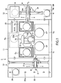
- FIG. 1 is a schematic plan view illustrating a resist coating and developing system 1
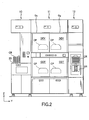
- FIG. 2 is a front view thereof
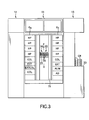
- FIG. 3 is a back view thereof.
- the resist coating and developing system 1 comprises a cassette station 10 as a convey station, a process station 11 having a plurality of process units, and an interface station 12 for transferring a wafer W to a non-illustrated exposure apparatus provided adjacent to the process station 11.
- the cassette station 10 has a cassette-placing table 20 where a wafer cassette CR capable of retaining a plurality of wafers (for instance, 25 wafers) is placed on the cassette-placing table 20.
- a wafer cassette CR accommodating wafers W to be processed in the resist coating and developing system 1 is conveyed to the cassette-placing table 20 of the cassette station 10 from another system.
- a wafer cassette CR accommodating wafers W having already been processed in the resist coating and developing system 1 is carried out to another system from the cassette-placing table 20.
- a plurality of positioning projections 20a are formed on the cassette-placing table 20 along an X direction in FIG. 1.
- Wafer cassettes CR are placed in a line at the locations of the positioning projections 20a, with their wafer outlet/inlet ports facing toward the process station 11.
- the wafers W are arranged in approximately horizontal postures along a vertical direction (Z direction) at predetermined intervals.
- the cassette station 10 also has a wafer conveying mechanism 21 which conveys the wafer W between the cassette-placing table 20 and the process station 11.
- the wafer conveying mechanism 21 is movable in the layout direction of the wafers W in the wafer cassette CR (Z direction) and the cassette layout direction (X direction), and has a wafer-conveying pick 21a which is movable back and forth in a Y direction perpendicular to the Z and X directions, and is rotatable in a horizontal plane (X-Y plane).
- the wafer-conveying pick 21a can selectively access wafers W accommodated at predetermined positions in the wafer cassette CR placed on the cassette-placing table 20, and can also access an alignment unit (ALIM) and an extension unit (EXT) belonging to a third process section G 3 of the process station 11 to be described later.
- ALIM alignment unit
- EXT extension unit
- the process station 11 has the plurality of process units for carrying out a series of processes when a resist coating and development of a resist liquid are carried out for the wafer W.
- the plurality of process units are arranged in multiple stages at predetermined positions. In each process unit, the wafers W are processed one by one.
- the process station 11 has a wafer-conveying passage 22a at the center portion thereof, while a main wafer conveying mechanism 22 is provided at the wafer-conveying passage 22a. All of the process units are provided around the wafer-conveying passage 22a.
- the plural process units are separated into a plurality of process sections in each of which a plurality of process units are laid out in multiple stages along the normal direction.
- the main wafer conveying mechanism 22 is structured that it has a wafer conveying device 76 elevatable in the normal direction inside a cylindrical support 79.
- the cylindrical support 79 is rotatable by the rotational driving force of a non-illustrated motor, while the wafer conveying device 76 can rotate integrally with the cylindrical support 79.
- the wafer conveying device 76 has a plurality of holding arms 78 movable in the back and forth directions of a convey base 77, whereby the exchange of the wafer W between the respective process units is enabled by the plurality of holding arms 78.
- the process sections G 1 , G 2 , G 3 and G 4 are actually laid out around the wafer-conveying passage 22a.
- the first and second process sections G 1 and G 2 among them are laid out in parallel with each other at the front side of the resist coating and developing system 1 (the front side in FIG. 1), the third process section G 3 is provided adjacent to the cassette station 10, while the fourth process section G 4 is provided adjacent to the interface station 12.
- a fifth process section G 5 can be laid out on the rear side of the resist coating and developing system 1.
- two of resist coating units (COT) of a spinner type which carries out a predetermined process on the wafer W placed on a spin chuck (not illustrated) in a coater cup (CP), and two developing units (DEV) of a spinner type, which develop a pattern of a resist, are placed one on the other in two stages in order from the bottom.
- two resist coating units (COT) of a spinner type and two developing units (DEV) of a spinner type are placed one on the other in two stages in order from the bottom. It is to be noted that the structure of the resist coating unit (COT) will be explained later in detail.
- multiple oven type process units which carry out a predetermined process on the wafer W placed on a susceptor SP are placed one on another in multiple stages.
- an adhesion unit (AD) which carries out a so-called hydrophobic process for enhancing the fixability of a resist
- an alignment unit (ALIM) for performing alignment
- an extension unit (EXT) which carries the wafer W in and out
- a cooling plate unit (COL) for performing a cooling process
- HP hot plate units which performs heat treatments on the wafer W coated with the resist liquid or the wafer W having undergone an exposure process are placed one on another another in eight stages in order from the bottom.
- a cooling unit (COL) may be provided in place of the alignment unit (ALIM) and may be provided with an alignment function.
- oven type process units are placed placed one on another in multiple stages. That is, a cooling plate unit (COL), an extension cooling plate unit (EXTCOL) as a wafer transfer member having a cooling plate, an extension unit (EXT), a cooling plate unit (COL), and four hot plate units (HP) are placed one on another in eight stages in order from the bottom.
- a cooling plate unit (COL)
- EXTCOL extension cooling plate unit
- COL cooling plate unit
- HP hot plate units
- the fifth process section G 5 When the fifth process section G 5 is provided on the rear side of the main wafer conveying mechanism 22, it is movable sideways as seen from the main wafer conveying mechanism 22 along a guide rail 25. Accordingly, even if the fifth process section G 5 is provided, a room can be secured by sliding it along the guide rail 25, so that a maintenance work for the main wafer conveying mechanism 22 can be easily carried out from the rear side thereof.
- the interface station 12 has such a structure that a portable pickup cassette PR and a fixed buffer cassette BR are laid out in two stages on its front side, a wafer edge exposure device 23 on a rear side thereof, and a wafer conveying mechanism 24 at the center portion thereof,.
- the wafer conveying mechanism 24 has a wafer-conveying arm 24a.
- the wafer-conveying arm 24a can move in the Z direction so that it can access both of the cassettes PR and BR, the wafer edge exposure device 23, the extension unit (EXT) included in the fourth process section G 4 of the process station 11, and a wafer transfer table (not illustrated) of the exposure apparatus adjacent to the interface station 12, respectively, while it is rotatable in the horizontal plane and is movable back and forth in the horizontal plane.
- the wafer cassette CR accommodating the wafers W to be processed is placed on the cassette-placing table 20, the wafer-conveying pick 21a accesses the wafer cassette CR, takes one of the wafers W out therefrom, and then conveys the wafer W to the extension unit (EXT) of the third process section G 3 .
- EXT extension unit
- the wafer W is carried into the process station 11 from the extension unit (EXT) by the wafer conveying device 76 of the main wafer conveying mechanism 22.
- the wafer W is aligned by the alignment unit (ALIM) of the third process section G 3 , conveyed to the adhesion unit (AD), and then a hydrophobic process (HMDS process) is performed in order to enhance the fixability of a resist.
- ALIM alignment unit
- AD adhesion unit
- HMDS process hydrophobic process
- the wafer W after the HMDS process is conveyed to the cooling plate unit (COL) by the wafer conveying device 76, and then cooled down there.
- the wafer W cooled down at the cooling plate unit (COL) after processed in the adhesion unit (AD), or a wafer W which has not been processed yet by the adhesion unit (AD) is conveyed to the resist coating unit (COT) by the wafer conveying device 76, coated with a resist liquid, thereby forming a resist film (film).
- the wafer W is conveyed to the hot plate unit (HP) of the third process section G 3 or the fourth process section G 4 , pre-baked, and conveyed to one of the cooling plate units (COL) to be cooled down.
- HP hot plate unit
- COL cooling plate units
- the wafer W is conveyed to the alignment unit (ALIM) of the third process section G 3 , aligned, and then conveyed to the interface station 12 via the extension unit (EXT) of the fourth process section G 4 .
- ALIM alignment unit
- EXT extension unit
- a wafer edge exposure process is performed on the wafer W by the wafer edge exposure device 23, thereby removing an excessive resist.
- the wafer W is then conveyed to the exposure apparatus (not illustrated) provided next to the interface station 12, and an exposure process is performed on the resist film on the wafer W in a predetermined pattern.
- the wafer W exposed is returned to the interface station 12, and then conveyed to the extension unit (EXT) included in the fourth process section G 4 by the wafer conveying mechanism 24.
- the wafer W is conveyed to the hot plate unit (HP) of the third or fourth process section G 3 or G 4 by the wafer conveying device 76, and post-exposure baking is performed thereon. While the wafer is cooled down to a predetermined temperature in the post-exposure baking, it may be conveyed to the cooling plate unit (COL) and cooled down, as needed.
- the wafer W is conveyed to the developing unit (DEV) where the exposed pattern is developed. After the development, the wafer W is conveyed to the hot plate unit (HP) of the third process section G 3 where post baking is performed.
- the wafer W which has undergone such a series of processes is returned to the cassette station 10 via the extension unit (EXT) of the third process section G 3 and accommodated at a predetermined position in the wafer cassette CR.
- FIG. 4 is a schematic cross-sectional view illustrating an embodiment of the resist coating unit (COT), while FIG. 5 is an enlarged view illustrating an area A in FIG. 4.
- the resist coating unit (COT) comprises a spin chuck 41 holding the wafer W in an approximately horizontal posture, a rotation mechanism 42 which rotates the spin chuck 41, a lift mechanism 43 which lifts the spin chuck 41 up and down, a process cup 50 which accommodates the spin chuck 41, and a resist coating nozzle 91 which supplies a resist liquid to the top surface of the wafer W held by the spin chuck 41.
- a non-illustrated filter fun unit (FFU) provides a clean air from above the process cup 50 as a downflow toward the process cup 50.
- the resist coating nozzle 91 is held by a nozzle holding arm 92.
- the nozzle holding arm 92 is movable between the center portion of the wafer W and a standby position (not shown) outside the process container by a nozzle moving mechanism 93, comprises a horizontal direction moving mechanism such as a slide mechanism or a rotation mechanism, and a lift mechanism (vertical directional moving mechanism). Moreover, the nozzle holding arm 92 can move close to or away from the top surface of the wafer W.
- the resist liquid is supplied to the resist coating nozzle 91 by a resist-liquid supply device 94.
- the spin chuck 41 chucks and holds the wafer W in a vacuuming manner by a non-illustrated chuck mechanism.
- the wafer W is chucked and held by the spin chuck 41, and a predetermined amount of a resist liquid is supplied to the substantial center of the wafer W, after which the spin chuck 41 is rotated by the rotation mechanism 42, thereby forming the resist film on the wafer W.
- the process cup 50 collects an excessive resist liquid dispersed around the wafer W from the wafer W.
- the process cup 50 generally comprises a first cup 51 so provided as to surround the outside of the wafer W, an airflow control member 52 so provided as to surround the wafer W in the first cup 51 in the vicinity of the wafer W, and a second cup 53 provided below the wafer W.
- the airflow control member 52 is connected to and held to the first cup 51 by link members (not illustrated) provided at plural locations on the periphery thereof.
- the first cup 51 has an outer circumferential wall 61a including a cylindrical first vertical wall 71a and a first inclined wall 71b connected in a consecutive arrangement to an upper end of the first vertical wall 71a and inclined inwardly and upward, a cylindrical middle wall 61b provided inwardly of the first vertical wall 71a, and a bottom wall 61c.
- the airflow control member 52 has a cross section of an approximately rectangular shape defined by an upper ring portion 62a having a cross section of an approximately triangular shape and protruding upward, and a lower ring portion 62b having a cross section of an approximately triangular shape and protruding downward.
- the upper and lower ring portions 62a, 62b may be formed integral with each other.
- the second cup 53 has a second inclined wall 63a expanding outward from below the wafer W toward an obliquely downward and outward, a cylindrical second vertical wall 63b connected in a consecutive arrangement to the lower end of the second inclined wall 63a, and a cylindrical inner periphery wall 63c provided inwardly of the middle wall 61b of the first cup 51.
- an exhaust passage 55 is formed between the outer circumferential wall 61a and the airflow control member 52, a drain passage 56 between the lower ring portion 62b and the second inclined wall 63a, an exhaust/drain passage 57 where the exhaust passage 55 and the drain passage 56 to be merged with each other is formed between the first vertical wall 71a and the second vertical wall 63b, a drain room 58 is formed between the outer circumferential wall 61a and the middle wall 61b, and an exhaust room 59 is formed between the middle wall 61b and the inner wall 63c.
- a rain port 74 is formed at that portion of the bottom wall 61c where the drain room 58 is formed, while an exhaust port 72 is formed at that portion the bottom wall 61c where the exhaust room 59 is formed.
- a drain tube 75 is attached to the drain port 74, while an exhaust tube 73 is attached to the exhaust port 72.
- a non-illustrated exhaust apparatus is provided at the downstream of the exhaust tube 73, and the atmosphere around the wafer W is exhausted from the bottom thereof via the exhaust port 72 by the activation of the exhaust apparatus.
- the exhausting of the atmosphere around the wafer W is substantially carried out via the exhaust passage 55, while the draining of the resist liquid dispersed from the wafer W when rotated is substantially carried out via the drain passage 56.
- an exhaust port 55a in the exhaust passage 55 (hereinafter, “atmosphere extraction port”) is formed between an upper end portion of the first inclined wall 71b of the first cup 51 and an apex of the upper ring portion 62a of the airflow control member 52. That is, in the resist coating unit (COT), the atmosphere extraction port 55a is provided outward and upward of the wafer W. Moreover, a resist liquid inlet 56a for allowing a resist liquid to flow into the drain passage 56 is formed between the wafer W and the airflow control member 52.
- the airflow control member 52 is laid out close to the wafer W in such a way that a width ⁇ of the resist liquid inlet 56a is narrower than a width a 1 of the atmosphere extraction port 55a. Accordingly, the atmosphere around the wafer W is likely to flow into the exhaust passage 55 via the atmosphere extraction port 55a, but it is difficult to flow into the drain passage 56 via the resist liquid drain port 56a. Thus way, the exhausting of the atmosphere around the wafer W is substantially carried out by the exhaust passage 55.
- the airflow control member 52 should preferably be provided in such a way that the height position of the vertex defined by mated inner corners of the upper and lower ring portions 62a and 62b is higher by, for instance, about 0.1 mm to 1 mm than the height position of the surface of the wafer W held by the spin chuck 41, so that the resist liquid dispersed from the wafer W with the spin chuck 41 rotated substantially hits the inner inclined wall of the lower ring portion 62b and guided to the drain passage 56, or the airflow flowing near the periphery of the wafer W substantially ascends along the inner inclined wall of the upper ring portion 62a and then flows into the exhaust passage 55 via the atmosphere extraction port 55a. Accordingly, the effect of making the thickness distribution more uniform can be ensured more notably.
- the airflow control member 52 is laid out so that its apex (the apex of the upper ring portion 62a) is positioned lower than the top end of the first cup 51 (the highest portion of the first inclined wall 71b) so that the airflow from the wafer W is easier to flow into the atmosphere extraction port 55a.
- an inner base angle ⁇ 1 of the upper ring portion 62a constituting the airflow control member 52 be larger than or equal to 24 degrees, but smaller than or equal to 34 degrees.
- the base angle ⁇ 1 of the upper ring portion 62a is smaller than 24 degrees, the position of the atmosphere extraction port 55a drops and comes close to the wafer W, increasing the influence of the airflow, flowed to the exhaust passage 55, on the wafer W.
- the base angle ⁇ 1 of the upper ring portion 62a becomes larger than 34 degree, the airflow directed from the center of the wafer W toward the periphery thereof hits the inner inclined wall of the upper ring portion 62a and is likely to return to the center portion. This makes it easier to cause contamination of the resist film due to the adhesion of a mist of the resist liquid contained in the airflow.
- An outer base angle ⁇ 3 of the upper ring portion 62a is determined according to the inclined angle of the first inclined wall 71b so as to ensure a predetermined width of the exhaust passage 55. For instance, it can be set in a range of larger than or equal to 22 degrees, and smaller than or equal to 32 degrees.
- the height of the upper ring portion 62a is set to a suitable value in accordance with the size of the wafer W as needed. For instance, when the diameter of the wafer W is 300 mm, the height ⁇ 2 of the upper ring portion 62a can be set greater than or equal to 10 mm, and less than or equal to 18 mm (for instance, 14 mm).
- an inner base angle ⁇ 2 of the lower ring portion 62b constituting the airflow control member 52 be larger than or equal to 25 degree, and smaller than or equal to 35 degrees.
- the base angle ⁇ 2 of the lower ring portion 62b is larger than 35 degrees, the resist liquid dispersed from the wafer W hits the inner inclined wall of the lower ring portion 62b and bounces, whereby the periphery of the wafer W is likely to be contaminated.
- the base angle ⁇ 2 is smaller than 25 degrees, the resist liquid dispersed and an airflow generated by the scattering of the resist liquid may reach the exhaust passage 55, so that the airflow at the exhaust passage 55 is disturbed, resulting in possible counterflow of the exhausted airflow.
- a width ⁇ 3 of the exhaust/drain passage 57 should preferably be narrower than a width ⁇ 1 of that portion of the exhaust passage 55 which is formed between the first vertical wall 71a and the lower ring portion 62b. Further, the width ⁇ 3 of the exhaust/drain passage 57 should preferably be narrower than a width ⁇ 2 of the drain passage 56. This is to prevent the disturbance of the airflow, which is likely to occur as the suction force at the exhaust/drain passage 57 is weakened, if the width ⁇ 3 of the exhaust/drain passage 57 is widened.
- the counterflow of the airflow flowed into the exhaust passage 55 be suppressed by providing a protrusion 61d protruding toward the atmosphere extraction port 55a on the upper end portion of the first inclined wall 71b of the first cup 51.
- the processing of the wafer W ino the resist coating unit (COT) with the above-described structure is carried out by steps to be discussed below.
- the holding arms 78 holding the wafer W is moved over the spin chuck 41, then the spin chuck 41 is lifted up, causing the wafer W to be held by the spin chuck 41.
- the spin chuck 41 is lifted down to hold the wafer W at the process height.
- the resist coating nozzle 91 is moved to the center of the wafer W and a predetermined amount of the resist liquid is supplied to the top surface of the wafer W, and then the spin chuck 41 is rotated. Accordingly, the resist liquid is centrifugally spread to the periphery of the wafer W, and the downflow to the wafer W and the airflow generated around the wafer W accelerate drying of the resist film.
- a part of the resist liquid dispersed from the wafer W may adhere to the inner inclined wall of the upper ring portion 62a of the airflow control member 52, but the resist liquid adhered to the airflow control member 52 can be removed when the process cup 50 is cleaned.
- pre-processing such as applying a solvent like a thinner to the top surface of the wafer W prior to the coating of the resist liquid on the wafer W.
- the spin chuck 41 stops rotating, it is lifted up to a predetermined height, while the holding arms 78 is moved under the spin chuck 41. Next, the spin chuck 41 is lifted down, during which the wafer W is transferred to the holding arms 78 from the spin chuck 41.
- the holding arms 78 carries the holding wafer W held to one of the hot plate units (HP), where pre-baking is performed on the wafer W
- Table 1 and FIGS. 7 and 8 show results, such as film thickness distributions, when the resist films were formed on the wafers W of 300 mm ⁇ using various process cups shown in FIGS. 6A to 6C while changing the rotation speed of the spin chuck 41.
- FIGS. 6A to 6C illustrate a portion outside and near the wafer W, and the structures of the other portions are the same.
- the process cup of Comparative Example 1 illustrated in FIG. 6A roughly has a modified structure of the process cup 50 from which the airflow control member 52 is removed and in which the leading end of the first inclined wall 71b of the first cup 51 is set close to the periphery of the wafer W.
- the first cup constituting the process cup of the Comparative Example 1 is denoted by reference number "89".
- first cup 89' The process cup of an Example shown in FIG. 6C is the same as the process cup 50 shown in FIGS. 4 and 5.
- Table 1 represents values of ranges of the measuring results and 3 ⁇ .
- the "range” represents a difference between a maximum value measured and a minimum value measured.
- the maximum value of the film thickness is a value at the outermost circumference (that is, at the circumference 3 mm inside the periphery of the wafer W)
- a small value of the range indicates small beaking of the resist film at the periphery.
- “3 ⁇ ” represents a standard deviation of the thickness distribution, and a small value thereof indicates that the resist film has a good uniformity of thickness.
- Comparative Example 2 As shown in Table 1, the values of the ranges and 3 ⁇ of Comparative Example 2 are smaller than those of the Comparative Example 1, and the values of the Example are further smaller. This seems to have occurred because in Comparative Examples 1 and 2, as the atmosphere extraction port was positioned close to the end face of the wafer W compared to the Example, the resist film at the periphery of the wafer W was likely to be dried due to the influence of the exhausted airflow, thereby making the resist film thicker. It would appear that regarding Comparative Example 1, the resist film became thicker at the periphery of the wafer W compared to Comparative Example 2 as the airflow flowing vertically hit the periphery of the wafer W so as to dry the resist film.
- FIG. 7 is a graph representing the values of the ranges and 3 ⁇ at points of 2 mm, 3 mm, and 5 mm in the inside of the periphery of the wafer W for Comparative Example 2 and the Example. As is apparent from FIG. 7, the beaking of the resist film at the periphery of the wafer W is suppressed for the Example.
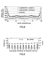
- FIG. 8 shows changes in the thicknesses of the resist films in the radial direction of the wafers W with the number of rotations of the spin chuck 41 of 8000 rpm.
- the beaking of the resist film at the periphery of the wafer W is suppressed for the Example.
- a resist film having a uniform thickness can be formed on the wafer W by using the process cup 50 of the Example.
- the overall film thickness is 10 nm thinner than those of Comparative Examples 1 and 2, but can be narrowed down to a predetermined thickness by adjusting the number of rotations and a turnover time.
- FIG. 9 represents results (the range and 3 ⁇ ) of measuring the resist film thickness measured at plural locations within the circumference 3 mm inside the periphery of the wafer W on the diameter, with a constant number of rotations of the spin chuck 41 and with points over the circumference taken as outermost circumference measurement points, while changing the exhaust pressure at the exhaust port 72. It was confirmed that when the exhaust pressure at the exhaust port 72 was changed, the pressures at the exhaust passage 55 and the drain passage 56 were also changed, but the influence of such a change in pressure hardly occurs on the thickness of the resist film as illustrated in FIG. 9. This means that the atmosphere around the wafer W can be exhausted with the thickness of the resist film held constant.
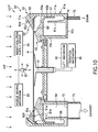
- FIG. 10 is a schematic cross-sectional view illustrating a resist coating unit (COT)' having a process cup 50' with an airflow control member 52'.
- This resist coating unit (COT)' and the previously described resist coating unit (COT) employ the same structure except that the shapes of their airflow control members of the process cups differ from each other.
- the airflow control member 52' of the process cup 50' comprises the upper ring portion 62a having a vertical cross section of an approximately triangular shape and protruding upward, and a lower ring portion 62b' which has a first inclined portion 81a outward and downward inclined from an inner apex of the upper ring portion 62a by a predetermined length, a horizontal portion 81b horizontally extending from the lower end of the first inclined portion 81a toward the outside thereof, and a second inclined portion 81c outward and downward inclined from the outer end of the horizontal portion 81b.
- the upper and lower ring portions 62a and 62b' should preferably be integrated with each other.
- the upper ring portion 62a is common to the process cup 50 and the process cup 50'.
- the first inclined portion 81a of the lower ring portion 62b' serves to guide the resist liquid dispersed from the wafer W downward.
- the width of a drain passage 56' formed between the second cup 53 and the lower ring portion 62b' is wider compared to the process cup 50.
- the wider width does not adversely affect the drain/exhaust property. Accordingly, the uniformity of the thickness of the resist film formed on the wafer W can be also enhanced by using the resist coating unit (COT)' equipped with the process cup 50' having the airflow control member 52'.
- the holding arms 78 is elevatable, the position where the wafer W is held may be fixed without lifting the spin chuck 41 up and down, and the process cup 50 may be lifted up and down in such a way as not to interfere with the transfer of the wafer W when the wafer W is transferred between the spin chuck 41 and the holding arms 78.
- the substrate is not limited to the semiconductor wafer, and may be a glass substrate for FPD (Flat Panes Display).
- the coating liquid is not limited to the resist liquid, and may be, for instance, a chemical solution to be used in forming an interlayer insulation film by spin coating.
- the coating process apparatus of the present invention is suitable for forming a coating film, such as a resist film, on a substrate such as a semiconductor wafer.
Landscapes
- Physics & Mathematics (AREA)
- General Physics & Mathematics (AREA)
- Exposure Of Semiconductors, Excluding Electron Or Ion Beam Exposure (AREA)
- Coating Apparatus (AREA)
- Materials For Photolithography (AREA)
Applications Claiming Priority (3)
| Application Number | Priority Date | Filing Date | Title |
|---|---|---|---|
| JP2002376233A JP4318913B2 (ja) | 2002-12-26 | 2002-12-26 | 塗布処理装置 |
| JP2002376233 | 2002-12-26 | ||
| PCT/JP2003/016154 WO2004059709A1 (ja) | 2002-12-26 | 2003-12-17 | 塗布処理装置および塗布膜形成方法 |
Publications (2)
| Publication Number | Publication Date |
|---|---|
| EP1577930A1 true EP1577930A1 (de) | 2005-09-21 |
| EP1577930A4 EP1577930A4 (de) | 2010-01-06 |
Family
ID=32677357
Family Applications (1)
| Application Number | Title | Priority Date | Filing Date |
|---|---|---|---|
| EP03780822A Withdrawn EP1577930A4 (de) | 2002-12-26 | 2003-12-17 | Beschichtungsvorrichtung und herstellungsverfahren für beschichtungsfilm |
Country Status (7)
| Country | Link |
|---|---|
| US (2) | US7575634B2 (de) |
| EP (1) | EP1577930A4 (de) |
| JP (1) | JP4318913B2 (de) |
| KR (1) | KR100954901B1 (de) |
| CN (1) | CN100380584C (de) |
| AU (1) | AU2003289383A1 (de) |
| WO (1) | WO2004059709A1 (de) |
Cited By (2)
| Publication number | Priority date | Publication date | Assignee | Title |
|---|---|---|---|---|
| CN102319656A (zh) * | 2011-09-21 | 2012-01-18 | 上海先进半导体制造股份有限公司 | Hmds自动供应系统及其自动供应的方法 |
| WO2012059087A3 (de) * | 2010-11-07 | 2012-06-28 | Hans Bohnet | Anordnung zur herstellung von strukturierten substraten |
Families Citing this family (35)
| Publication number | Priority date | Publication date | Assignee | Title |
|---|---|---|---|---|
| JP4642543B2 (ja) * | 2005-05-09 | 2011-03-02 | 東京エレクトロン株式会社 | 周縁露光装置、塗布、現像装置及び周縁露光方法 |
| JP4796902B2 (ja) * | 2005-07-11 | 2011-10-19 | 芝浦メカトロニクス株式会社 | 基板のスピン処理装置 |
| JP4519035B2 (ja) * | 2005-08-30 | 2010-08-04 | 東京エレクトロン株式会社 | 塗布膜形成装置 |
| KR100689664B1 (ko) * | 2005-09-07 | 2007-03-08 | 삼성전자주식회사 | 웨이퍼 세정 장치 |
| US7762887B1 (en) | 2006-12-04 | 2010-07-27 | G&G Technologies LLC | Systems and methods for electronically managing games |
| CN101354534B (zh) * | 2007-07-27 | 2011-07-06 | 中芯国际集成电路制造(上海)有限公司 | 光刻胶的涂布方法及光刻图形的形成方法 |
| US8999106B2 (en) * | 2007-12-19 | 2015-04-07 | Applied Materials, Inc. | Apparatus and method for controlling edge performance in an inductively coupled plasma chamber |
| JP5084639B2 (ja) * | 2008-06-30 | 2012-11-28 | 芝浦メカトロニクス株式会社 | スピン処理装置 |
| JP5508709B2 (ja) * | 2008-12-22 | 2014-06-04 | 株式会社Sokudo | 塗布処理装置および基板処理装置 |
| JP2010287686A (ja) * | 2009-06-10 | 2010-12-24 | Tokyo Electron Ltd | 塗布、現像装置及び基板の裏面洗浄方法。 |
| KR20110106178A (ko) * | 2010-03-22 | 2011-09-28 | 삼성전자주식회사 | 기판 처리 장치 및 방법 |
| KR20110127055A (ko) * | 2010-05-18 | 2011-11-24 | 주식회사 에스앤에스텍 | 레지스트막 형성 장치, 포토마스크 블랭크 및 포토마스크 블랭크의 제조 방법 |
| JP5242635B2 (ja) * | 2010-06-29 | 2013-07-24 | 東京エレクトロン株式会社 | 塗布方法および塗布装置 |
| JP2012019025A (ja) * | 2010-07-07 | 2012-01-26 | Tokyo Electron Ltd | 液処理装置 |
| CN102707572A (zh) * | 2012-06-06 | 2012-10-03 | 长春理工大学 | 在凸球面上扫描喷涂光刻胶的装置及方法 |
| JP6093569B2 (ja) * | 2012-12-28 | 2017-03-08 | 株式会社荏原製作所 | 基板洗浄装置 |
| JP6281161B2 (ja) * | 2013-09-27 | 2018-02-21 | 東京エレクトロン株式会社 | 液処理装置 |
| US9817315B2 (en) | 2014-03-13 | 2017-11-14 | Taiwan Semiconductor Manufacturing Co., Ltd. | System and method for supplying and dispensing bubble-free photolithography chemical solutions |
| JP6461617B2 (ja) * | 2015-01-20 | 2019-01-30 | 株式会社Screenホールディングス | 基板処理装置 |
| DE102015104735A1 (de) * | 2015-03-27 | 2016-09-29 | Obducat Ab | Drehteller zur Aufnahme eines Substrats für eine Belackungsvorrichtung |
| WO2016179818A1 (en) * | 2015-05-14 | 2016-11-17 | Acm Research (Shanghai) Inc. | Apparatus for substrate bevel and backside protection |
| KR102542886B1 (ko) * | 2016-04-25 | 2023-06-12 | 동우 화인켐 주식회사 | 코팅용 지그 및 이를 이용한 코팅 방법 |
| JP6925213B2 (ja) * | 2017-09-22 | 2021-08-25 | 東京エレクトロン株式会社 | 加熱処理装置及び加熱処理方法 |
| KR102447277B1 (ko) * | 2017-11-17 | 2022-09-26 | 삼성전자주식회사 | 스핀 코터 및 이를 구비하는 기판처리 장치와 기판처리 시스템 |
| KR102353775B1 (ko) * | 2019-11-27 | 2022-01-20 | 세메스 주식회사 | 기판처리장치 |
| US12198944B2 (en) | 2020-11-11 | 2025-01-14 | Applied Materials, Inc. | Substrate handling in a modular polishing system with single substrate cleaning chambers |
| KR102634281B1 (ko) | 2020-12-21 | 2024-02-07 | 세메스 주식회사 | 기판 처리 장치 |
| KR102677969B1 (ko) * | 2020-12-30 | 2024-06-26 | 세메스 주식회사 | 노즐 대기 포트와 이를 포함하는 기판 처리 장치 및 이를 이용한 노즐 세정 방법 |
| KR102853348B1 (ko) * | 2021-01-27 | 2025-08-29 | 삼성전자주식회사 | 기판 처리 장치 |
| JP7628434B2 (ja) | 2021-02-15 | 2025-02-10 | 株式会社Screenホールディングス | 基板処理装置、および、筒状ガードの加工方法 |
| CN113655688A (zh) * | 2021-09-08 | 2021-11-16 | 深圳市龙图光电有限公司 | 掩模版制造装置 |
| TWI913513B (zh) * | 2021-11-04 | 2026-02-01 | 日商東京威力科創股份有限公司 | 基板處理裝置及基板處理方法 |
| US12517435B2 (en) * | 2022-01-19 | 2026-01-06 | Taiwan Semiconductor Manufacturing Company, Ltd. | Method for spin-coating a layer on a semiconductor wafer |
| JP7780381B2 (ja) * | 2022-04-14 | 2025-12-04 | 東京エレクトロン株式会社 | カップ及び基板処理装置 |
| CN117198938B (zh) * | 2023-09-15 | 2025-08-19 | 华海清科股份有限公司 | 一种晶圆后处理装置 |
Family Cites Families (99)
| Publication number | Priority date | Publication date | Assignee | Title |
|---|---|---|---|---|
| JPS6439023A (en) * | 1987-08-05 | 1989-02-09 | Seiko Epson Corp | Structure for preventing splashing in rotating body |
| JPH0421467Y2 (de) | 1987-09-02 | 1992-05-15 | ||
| JP2907877B2 (ja) * | 1989-07-31 | 1999-06-21 | 株式会社日立製作所 | 塗布装置および塗布方法 |
| US5297031A (en) * | 1990-03-06 | 1994-03-22 | Chicago Board Of Trade | Method and apparatus for order management by market brokers |
| DE69115762T2 (de) * | 1990-06-19 | 1996-06-13 | Fujitsu Ltd | Verfahren und Einrichtung zur Anzeigesteuerung von Mehrfenstern |
| JPH0699125A (ja) | 1992-09-24 | 1994-04-12 | Mitsubishi Plastics Ind Ltd | スピンコーターおよび光ディスクの製造方法 |
| JPH0917722A (ja) * | 1995-06-27 | 1997-01-17 | Hitachi Ltd | 塗布装置 |
| JPH0910658A (ja) * | 1995-06-27 | 1997-01-14 | Hitachi Ltd | 塗布方法および塗布装置 |
| JPH0945611A (ja) * | 1995-07-27 | 1997-02-14 | Dainippon Screen Mfg Co Ltd | 回転式基板塗布装置 |
| US6209004B1 (en) * | 1995-09-01 | 2001-03-27 | Taylor Microtechnology Inc. | Method and system for generating and distributing document sets using a relational database |
| JP3589518B2 (ja) | 1995-11-30 | 2004-11-17 | 大日本スクリーン製造株式会社 | 基板処理装置 |
| US6519574B1 (en) * | 1995-12-12 | 2003-02-11 | Reuters Limited | Electronic trading system featuring arbitrage and third-party credit opportunities |
| JP2000508796A (ja) * | 1996-04-12 | 2000-07-11 | シティバンク、エヌ・エイ | インサイドマネー |
| US6014643A (en) * | 1996-06-28 | 2000-01-11 | Minton; Vernon F. | Interactive securities trading system |
| US6029146A (en) * | 1996-08-21 | 2000-02-22 | Crossmar, Inc. | Method and apparatus for trading securities electronically |
| US6016483A (en) * | 1996-09-20 | 2000-01-18 | Optimark Technologies, Inc. | Method and apparatus for automated opening of options exchange |
| US6850907B2 (en) * | 1996-12-13 | 2005-02-01 | Cantor Fitzgerald, L.P. | Automated price improvement protocol processor |
| US5873071A (en) * | 1997-05-15 | 1999-02-16 | Itg Inc. | Computer method and system for intermediated exchange of commodities |
| US20070061452A1 (en) * | 1997-05-23 | 2007-03-15 | The Thomson Corporation | Market data notification system |
| US6996540B1 (en) * | 1997-10-14 | 2006-02-07 | Blackbird Holdings, Inc. | Systems for switch auctions utilizing risk position portfolios of a plurality of traders |
| US6535917B1 (en) * | 1998-02-09 | 2003-03-18 | Reuters, Ltd. | Market data domain and enterprise system implemented by a master entitlement processor |
| US6343278B1 (en) * | 1998-09-04 | 2002-01-29 | Ebs Dealing Resources, Inc. | Combined order limit for a group of related transactions in an automated dealing system |
| US7020632B1 (en) * | 1999-01-11 | 2006-03-28 | Lawrence Kohls | Trading system for fixed-value contracts |
| US6513019B2 (en) * | 1999-02-16 | 2003-01-28 | Financial Technologies International, Inc. | Financial consolidation and communication platform |
| US6993504B1 (en) * | 1999-04-09 | 2006-01-31 | Trading Technologies International, Inc. | User interface for semi-fungible trading |
| US7212999B2 (en) * | 1999-04-09 | 2007-05-01 | Trading Technologies International, Inc. | User interface for an electronic trading system |
| US6505175B1 (en) * | 1999-10-06 | 2003-01-07 | Goldman, Sachs & Co. | Order centric tracking system |
| JP3599323B2 (ja) | 1999-10-19 | 2004-12-08 | 東京エレクトロン株式会社 | 基板処理装置 |
| US6527860B1 (en) * | 1999-10-19 | 2003-03-04 | Tokyo Electron Limited | Substrate processing apparatus |
| SG185822A1 (en) * | 2000-02-01 | 2012-12-28 | Tokyo Electron Ltd | Substrate processing apparatus and substrate processing method |
| JP2002110517A (ja) | 2000-09-28 | 2002-04-12 | Toshiba Corp | 液体除去方法 |
| US6579382B2 (en) * | 2000-02-17 | 2003-06-17 | Kabushiki Kaisha Toshiba | Chemical liquid processing apparatus for processing a substrate and the method thereof |
| US20020026401A1 (en) * | 2000-02-21 | 2002-02-28 | Hueler Kelli Hustad | System and method for facilitating electronic bidding between buyers and sellers in financial industries |
| US7389268B1 (en) * | 2000-03-02 | 2008-06-17 | Trading Technologies International, Inc. | Trading tools for electronic trading |
| US6938011B1 (en) * | 2000-03-02 | 2005-08-30 | Trading Technologies International, Inc. | Click based trading with market depth display |
| US7127424B2 (en) * | 2000-03-02 | 2006-10-24 | Trading Technologies International, Inc. | Click based trading with intuitive grid display of market depth and price consolidation |
| US6772132B1 (en) * | 2000-03-02 | 2004-08-03 | Trading Technologies International, Inc. | Click based trading with intuitive grid display of market depth |
| US7003486B1 (en) * | 2000-04-17 | 2006-02-21 | Neha Net Corp. | Net-value creation and allocation in an electronic trading system |
| US6868400B1 (en) * | 2000-05-24 | 2005-03-15 | Nehanet Corp. | Spread-maximizing travel-services trading system using buyer- and seller-specified multi-attribute values |
| US7437325B2 (en) * | 2002-03-05 | 2008-10-14 | Pablo Llc | System and method for performing automatic spread trading |
| WO2002003302A1 (en) * | 2000-06-30 | 2002-01-10 | Enron Net Works Llc | Buying and selling goods and services using automated method and apparatus |
| US7177833B1 (en) * | 2000-07-18 | 2007-02-13 | Edge Capture, Llc | Automated trading system in an electronic trading exchange |
| NO312427B1 (no) * | 2000-08-04 | 2002-05-06 | Usertrade As | Elektronisk handelssystem |
| AUPQ950400A0 (en) * | 2000-08-17 | 2000-09-07 | Peruch, Stephen Sebastian | Computer implemented system and method of transforming a source file into transformed file using a set of trigger instructions |
| WO2002037390A2 (en) * | 2000-10-30 | 2002-05-10 | Liquidity Direct Technology | Network and method for trading derivatives |
| US7184984B2 (en) * | 2000-11-17 | 2007-02-27 | Valaquenta Intellectual Properties Limited | Global electronic trading system |
| GB2376319A (en) * | 2001-06-05 | 2002-12-11 | Security & Standards Ltd | Validation System |
| US20030009419A1 (en) * | 2001-06-11 | 2003-01-09 | Chavez R. Martin | Risk management system and trade engine with automatic trade feed and market data feed |
| US7702563B2 (en) * | 2001-06-11 | 2010-04-20 | Otc Online Partners | Integrated electronic exchange of structured contracts with dynamic risk-based transaction permissioning |
| CA2403300A1 (en) * | 2002-09-12 | 2004-03-12 | Pranil Ram | A method of buying or selling items and a user interface to facilitate the same |
| US7650305B1 (en) * | 2001-10-03 | 2010-01-19 | I2 Technologies Us, Inc. | Displaying market data |
| US7672895B2 (en) * | 2002-02-19 | 2010-03-02 | Trading Technologies International, Inc. | System and method for simulating an electronic trading environment |
| US8666869B2 (en) * | 2002-08-06 | 2014-03-04 | Redi Tech, Llc | Systems for electronic trading |
| EP1552458A4 (de) * | 2002-10-15 | 2006-01-25 | Chicago Mercantile Exchange | Netzwerk und verfahren zum handeln mit derivativen durch bereitstellen erweiterter rfq-visibilität |
| US7426490B1 (en) * | 2002-10-31 | 2008-09-16 | Trading Technologies International, Inc. | System and method for automated order entry on short queues |
| US7523064B2 (en) * | 2002-11-13 | 2009-04-21 | Trading Technologies International, Inc. | System and method for facilitating trading of multiple tradeable objects in an electronic trading environment |
| US7418422B2 (en) * | 2002-11-13 | 2008-08-26 | Trading Technologies International, Inc. | Method, apparatus and interface for trading multiple tradeable objects |
| US8041622B1 (en) * | 2002-11-26 | 2011-10-18 | Trading Technologies International Inc. | System and method for randomizing orders in an electronic trading environment |
| US7603303B1 (en) * | 2002-11-26 | 2009-10-13 | Trading Technologies International, Inc. | System and method for risk management |
| US7577602B2 (en) * | 2002-11-26 | 2009-08-18 | Trading Technologies International Inc. | Method and interface for consolidating price levels on a trading screen |
| US7769668B2 (en) * | 2002-12-09 | 2010-08-03 | Sam Balabon | System and method for facilitating trading of financial instruments |
| US7483854B2 (en) * | 2003-01-24 | 2009-01-27 | Liu Michael C | Method and system for intelligent automated security trading via the internet |
| US7512557B1 (en) * | 2003-06-30 | 2009-03-31 | Trading Technologies International, Inc. | System and method for timed order entry and modification |
| US7739182B2 (en) * | 2003-07-03 | 2010-06-15 | Makor Issues And Rights Ltd. | Machine learning automatic order transmission system for sending self-optimized trading signals |
| US7756782B2 (en) * | 2003-07-28 | 2010-07-13 | Trading Technologies International, Inc. | System and method for improved electronic trading |
| US7624063B1 (en) * | 2003-09-30 | 2009-11-24 | Trading Technologies International, Inc. | System and method for improved distribution of market information |
| US7668767B1 (en) * | 2003-10-01 | 2010-02-23 | Trading Technologies International, Inc. | System and method for dynamic quantity orders in an electronic trading environment |
| US7765143B1 (en) * | 2003-11-04 | 2010-07-27 | Trading Technologies International, Inc. | System and method for event driven virtual workspace |
| US7647266B1 (en) * | 2004-03-24 | 2010-01-12 | Trading Technologies International, Inc. | System and method for holding and sending an order to a matching engine |
| US7218325B1 (en) * | 2004-03-31 | 2007-05-15 | Trading Technologies International, Inc. | Graphical display with integrated recent period zoom and historical period context data |
| US7890396B2 (en) * | 2005-06-07 | 2011-02-15 | Cfph, Llc | Enhanced system and method for managing financial market information |
| US8232962B2 (en) * | 2004-06-21 | 2012-07-31 | Trading Technologies International, Inc. | System and method for display management based on user attention inputs |
| US20100076906A1 (en) * | 2004-07-12 | 2010-03-25 | Rosenthal Collins Group, L.L.C. | Method and system for using quantitative analytics on a graphical user interface for electronic trading |
| WO2006017243A2 (en) * | 2004-07-12 | 2006-02-16 | Rosenthal Collins Group, Llc | Method and system for providing a graphical user interface for electronic trading |
| WO2006036942A2 (en) * | 2004-09-27 | 2006-04-06 | Citadel Investment Group, L.L.C. | Providing guaranteed, specified and/or predetermined execution prices in a guaranteed, specified and/or predetermined timeframe on the purchase or sale of listed options |
| US7542938B1 (en) * | 2004-12-28 | 2009-06-02 | Trading Technologies International, Inc. | System and method for quick quote configuration |
| US7487125B2 (en) * | 2005-01-14 | 2009-02-03 | Littlewood Margaret G | Method for providing aggregation of trading on multiple alternative trading systems |
| USD539297S1 (en) * | 2005-05-05 | 2007-03-27 | Noviello Joseph C | User interface for an electronic trading system for a computer screen |
| USD559260S1 (en) * | 2005-05-05 | 2008-01-08 | Espeed Inc. | User interface for an electronic trading system for a computer screen |
| USD538815S1 (en) * | 2005-05-05 | 2007-03-20 | Noviello Joseph C | User interface for an electronic trading system for a computer screen |
| USD559259S1 (en) * | 2005-05-05 | 2008-01-08 | Espeed Inc. | User interface for an electronic trading system for a computer screen |
| USD538294S1 (en) * | 2005-05-05 | 2007-03-13 | Noviello Joseph C | User interface for an electronic trading system for a computer screen |
| USD538818S1 (en) * | 2005-05-05 | 2007-03-20 | Noviello Joseph C | User interface for an electronic trading system for a computer screen |
| USD538816S1 (en) * | 2005-05-05 | 2007-03-20 | Noviello Joseph C | User interface for an electronic trading system for a computer screen |
| USD538817S1 (en) * | 2005-05-05 | 2007-03-20 | Noviello Joseph C | User interface for an electronic trading system for a computer screen |
| USD538295S1 (en) * | 2005-05-05 | 2007-03-13 | Noviello Joseph C | User interface for an electronic trading system for a computer screen |
| US20100076907A1 (en) * | 2005-05-31 | 2010-03-25 | Rosenthal Collins Group, Llc. | Method and system for automatically inputting, monitoring and trading risk- controlled spreads |
| US7711630B2 (en) * | 2005-06-06 | 2010-05-04 | Trading Technologies International. Inc. | System and method for trading multiple tradeable objects using a single trading interface |
| US7565318B2 (en) * | 2005-06-28 | 2009-07-21 | Trading Technologies International, Inc. | System and method for calculating and displaying volume to identify buying and selling in an electronic trading environment |
| US20070016509A1 (en) * | 2005-07-15 | 2007-01-18 | Vogel Robert P | Computerized transaction-based yield curve analytics |
| US7933828B2 (en) * | 2005-07-26 | 2011-04-26 | Cfph, Llc | System and method for displaying and/or analyzing a limit order book |
| US7624066B2 (en) * | 2005-08-10 | 2009-11-24 | Tradehelm, Inc. | Method and apparatus for electronic trading of financial instruments |
| US20070043647A1 (en) * | 2005-08-16 | 2007-02-22 | American Stock Exchange Llc | Electronic trading environment with price improvement |
| US7672896B2 (en) * | 2005-09-30 | 2010-03-02 | Trading Technologies International, Inc. | System and method for order placement in an electronic trading environment |
| WO2007095742A1 (en) * | 2006-02-27 | 2007-08-30 | Lange David H | System and method for determining and brokering fuel emission offsets |
| US20080059846A1 (en) * | 2006-08-31 | 2008-03-06 | Rosenthal Collins Group, L.L.C. | Fault tolerant electronic trading system and method |
| US20100010937A1 (en) * | 2008-04-30 | 2010-01-14 | Rosenthal Collins Group, L.L.C. | Method and system for providing risk assessment management and reporting for multi-market electronic trading |
| US7844726B2 (en) * | 2008-07-28 | 2010-11-30 | Trading Technologies International, Inc. | System and method for dynamically managing message flow |
| US20100036704A1 (en) * | 2008-08-05 | 2010-02-11 | International Business Machines Corporation | Method and system for allocating requirements in a service oriented architecture using software and hardware string representation |
-
2002
- 2002-12-26 JP JP2002376233A patent/JP4318913B2/ja not_active Expired - Fee Related
-
2003
- 2003-12-17 CN CNB2003801075768A patent/CN100380584C/zh not_active Expired - Fee Related
- 2003-12-17 AU AU2003289383A patent/AU2003289383A1/en not_active Abandoned
- 2003-12-17 US US10/538,727 patent/US7575634B2/en not_active Expired - Fee Related
- 2003-12-17 WO PCT/JP2003/016154 patent/WO2004059709A1/ja not_active Ceased
- 2003-12-17 EP EP03780822A patent/EP1577930A4/de not_active Withdrawn
- 2003-12-17 KR KR1020057011969A patent/KR100954901B1/ko not_active Expired - Fee Related
-
2009
- 2009-06-25 US US12/491,424 patent/US7790227B2/en not_active Expired - Fee Related
Cited By (4)
| Publication number | Priority date | Publication date | Assignee | Title |
|---|---|---|---|---|
| WO2012059087A3 (de) * | 2010-11-07 | 2012-06-28 | Hans Bohnet | Anordnung zur herstellung von strukturierten substraten |
| US9508542B2 (en) | 2010-11-07 | 2016-11-29 | Rumailha-Comercio Internacional e Servicos LDA & Comandita | Arrangement for the production of structured substrates |
| CN102319656A (zh) * | 2011-09-21 | 2012-01-18 | 上海先进半导体制造股份有限公司 | Hmds自动供应系统及其自动供应的方法 |
| CN102319656B (zh) * | 2011-09-21 | 2013-06-12 | 上海先进半导体制造股份有限公司 | Hmds自动供应系统及其自动供应的方法 |
Also Published As
| Publication number | Publication date |
|---|---|
| KR100954901B1 (ko) | 2010-04-27 |
| JP2004207573A (ja) | 2004-07-22 |
| CN100380584C (zh) | 2008-04-09 |
| US7790227B2 (en) | 2010-09-07 |
| AU2003289383A1 (en) | 2004-07-22 |
| JP4318913B2 (ja) | 2009-08-26 |
| KR20050086941A (ko) | 2005-08-30 |
| WO2004059709A1 (ja) | 2004-07-15 |
| EP1577930A4 (de) | 2010-01-06 |
| US20090258139A1 (en) | 2009-10-15 |
| US7575634B2 (en) | 2009-08-18 |
| US20060068093A1 (en) | 2006-03-30 |
| CN1732555A (zh) | 2006-02-08 |
Similar Documents
| Publication | Publication Date | Title |
|---|---|---|
| US7790227B2 (en) | Coating process apparatus and coating film forming method | |
| JP4805758B2 (ja) | 塗布処理方法、プログラム、コンピュータ読み取り可能な記録媒体及び塗布処理装置 | |
| KR100604024B1 (ko) | 도포막 형성방법 및 도포장치 | |
| KR100497299B1 (ko) | 기판처리장치 | |
| KR101386377B1 (ko) | 기판처리장치 | |
| US6736556B2 (en) | Substrate processing apparatus | |
| JP3527426B2 (ja) | 現像処理方法および現像処理装置 | |
| KR19990013571A (ko) | 도포장치 | |
| US7419316B2 (en) | Developing treatment apparatus | |
| JP2003001182A (ja) | 塗布膜形成装置およびスピンチャック | |
| JP3811103B2 (ja) | 熱的処理装置および熱的処理方法 | |
| KR20010062438A (ko) | 막형성장치 | |
| JP4312997B2 (ja) | 基板処理装置、基板処理方法及びノズル | |
| JP4170943B2 (ja) | 基板処理装置 | |
| JP2003203837A (ja) | 基板処理方法及び基板処理装置 | |
| JP2003218015A (ja) | 基板処理装置 | |
| US8127713B2 (en) | Multi-channel developer system | |
| US7673582B2 (en) | Apparatus and method for removing an edge bead of a spin-coated layer | |
| KR102046872B1 (ko) | 기판 처리 장치 및 방법 | |
| JP3909574B2 (ja) | レジスト塗布装置 | |
| JP3485471B2 (ja) | 処理装置及び処理方法 | |
| JP4029066B2 (ja) | 基板処理装置 | |
| JP3352419B2 (ja) | 塗布膜形成方法および塗布処理システム | |
| JP2000146444A (ja) | 加熱処理装置 | |
| JP2000138276A (ja) | 基板処理装置 |
Legal Events
| Date | Code | Title | Description |
|---|---|---|---|
| PUAI | Public reference made under article 153(3) epc to a published international application that has entered the european phase |
Free format text: ORIGINAL CODE: 0009012 |
|
| 17P | Request for examination filed |
Effective date: 20050624 |
|
| AK | Designated contracting states |
Kind code of ref document: A1 Designated state(s): AT BE BG CH CY CZ DE DK EE ES FI FR GB GR HU IE IT LI LU MC NL PT RO SE SI SK TR |
|
| AX | Request for extension of the european patent |
Extension state: AL LT LV MK |
|
| DAX | Request for extension of the european patent (deleted) | ||
| A4 | Supplementary search report drawn up and despatched |
Effective date: 20091204 |
|
| 17Q | First examination report despatched |
Effective date: 20100419 |
|
| RIC1 | Information provided on ipc code assigned before grant |
Ipc: G03F 7/16 20060101ALI20120216BHEP Ipc: B05C 11/08 20060101ALI20120216BHEP Ipc: H01L 21/67 20060101ALI20120216BHEP Ipc: H01L 21/027 20060101AFI20120216BHEP |
|
| GRAP | Despatch of communication of intention to grant a patent |
Free format text: ORIGINAL CODE: EPIDOSNIGR1 |
|
| STAA | Information on the status of an ep patent application or granted ep patent |
Free format text: STATUS: THE APPLICATION IS DEEMED TO BE WITHDRAWN |
|
| 18D | Application deemed to be withdrawn |
Effective date: 20121009 |