EP1574881B1 - Optisches Element mit Antireflexfilm mit feinen Oberflächen-Unebenheiten, dessen Herstellungsverfahren - Google Patents
Optisches Element mit Antireflexfilm mit feinen Oberflächen-Unebenheiten, dessen Herstellungsverfahren Download PDFInfo
- Publication number
- EP1574881B1 EP1574881B1 EP05250988A EP05250988A EP1574881B1 EP 1574881 B1 EP1574881 B1 EP 1574881B1 EP 05250988 A EP05250988 A EP 05250988A EP 05250988 A EP05250988 A EP 05250988A EP 1574881 B1 EP1574881 B1 EP 1574881B1
- Authority
- EP
- European Patent Office
- Prior art keywords
- film
- alumina
- fine irregularities
- optical member
- thin film
- Prior art date
- Legal status (The legal status is an assumption and is not a legal conclusion. Google has not performed a legal analysis and makes no representation as to the accuracy of the status listed.)
- Expired - Fee Related
Links
Images


Classifications
-
- G—PHYSICS
- G02—OPTICS
- G02B—OPTICAL ELEMENTS, SYSTEMS OR APPARATUS
- G02B1/00—Optical elements characterised by the material of which they are made; Optical coatings for optical elements
- G02B1/10—Optical coatings produced by application to, or surface treatment of, optical elements
- G02B1/11—Anti-reflection coatings
-
- C—CHEMISTRY; METALLURGY
- C03—GLASS; MINERAL OR SLAG WOOL
- C03C—CHEMICAL COMPOSITION OF GLASSES, GLAZES OR VITREOUS ENAMELS; SURFACE TREATMENT OF GLASS; SURFACE TREATMENT OF FIBRES OR FILAMENTS MADE FROM GLASS, MINERALS OR SLAGS; JOINING GLASS TO GLASS OR OTHER MATERIALS
- C03C1/00—Ingredients generally applicable to manufacture of glasses, glazes, or vitreous enamels
- C03C1/006—Ingredients generally applicable to manufacture of glasses, glazes, or vitreous enamels to produce glass through wet route
- C03C1/008—Ingredients generally applicable to manufacture of glasses, glazes, or vitreous enamels to produce glass through wet route for the production of films or coatings
-
- C—CHEMISTRY; METALLURGY
- C03—GLASS; MINERAL OR SLAG WOOL
- C03C—CHEMICAL COMPOSITION OF GLASSES, GLAZES OR VITREOUS ENAMELS; SURFACE TREATMENT OF GLASS; SURFACE TREATMENT OF FIBRES OR FILAMENTS MADE FROM GLASS, MINERALS OR SLAGS; JOINING GLASS TO GLASS OR OTHER MATERIALS
- C03C17/00—Surface treatment of glass, not in the form of fibres or filaments, by coating
- C03C17/006—Surface treatment of glass, not in the form of fibres or filaments, by coating with materials of composite character
- C03C17/007—Surface treatment of glass, not in the form of fibres or filaments, by coating with materials of composite character containing a dispersed phase, e.g. particles, fibres or flakes, in a continuous phase
-
- C—CHEMISTRY; METALLURGY
- C03—GLASS; MINERAL OR SLAG WOOL
- C03C—CHEMICAL COMPOSITION OF GLASSES, GLAZES OR VITREOUS ENAMELS; SURFACE TREATMENT OF GLASS; SURFACE TREATMENT OF FIBRES OR FILAMENTS MADE FROM GLASS, MINERALS OR SLAGS; JOINING GLASS TO GLASS OR OTHER MATERIALS
- C03C17/00—Surface treatment of glass, not in the form of fibres or filaments, by coating
- C03C17/34—Surface treatment of glass, not in the form of fibres or filaments, by coating with at least two coatings having different compositions
- C03C17/3411—Surface treatment of glass, not in the form of fibres or filaments, by coating with at least two coatings having different compositions with at least two coatings of inorganic materials
- C03C17/3417—Surface treatment of glass, not in the form of fibres or filaments, by coating with at least two coatings having different compositions with at least two coatings of inorganic materials all coatings being oxide coatings
-
- C—CHEMISTRY; METALLURGY
- C03—GLASS; MINERAL OR SLAG WOOL
- C03C—CHEMICAL COMPOSITION OF GLASSES, GLAZES OR VITREOUS ENAMELS; SURFACE TREATMENT OF GLASS; SURFACE TREATMENT OF FIBRES OR FILAMENTS MADE FROM GLASS, MINERALS OR SLAGS; JOINING GLASS TO GLASS OR OTHER MATERIALS
- C03C2217/00—Coatings on glass
- C03C2217/40—Coatings comprising at least one inhomogeneous layer
- C03C2217/42—Coatings comprising at least one inhomogeneous layer consisting of particles only
-
- C—CHEMISTRY; METALLURGY
- C03—GLASS; MINERAL OR SLAG WOOL
- C03C—CHEMICAL COMPOSITION OF GLASSES, GLAZES OR VITREOUS ENAMELS; SURFACE TREATMENT OF GLASS; SURFACE TREATMENT OF FIBRES OR FILAMENTS MADE FROM GLASS, MINERALS OR SLAGS; JOINING GLASS TO GLASS OR OTHER MATERIALS
- C03C2217/00—Coatings on glass
- C03C2217/40—Coatings comprising at least one inhomogeneous layer
- C03C2217/425—Coatings comprising at least one inhomogeneous layer consisting of a porous layer
-
- C—CHEMISTRY; METALLURGY
- C03—GLASS; MINERAL OR SLAG WOOL
- C03C—CHEMICAL COMPOSITION OF GLASSES, GLAZES OR VITREOUS ENAMELS; SURFACE TREATMENT OF GLASS; SURFACE TREATMENT OF FIBRES OR FILAMENTS MADE FROM GLASS, MINERALS OR SLAGS; JOINING GLASS TO GLASS OR OTHER MATERIALS
- C03C2217/00—Coatings on glass
- C03C2217/40—Coatings comprising at least one inhomogeneous layer
- C03C2217/43—Coatings comprising at least one inhomogeneous layer consisting of a dispersed phase in a continuous phase
- C03C2217/46—Coatings comprising at least one inhomogeneous layer consisting of a dispersed phase in a continuous phase characterized by the dispersed phase
- C03C2217/47—Coatings comprising at least one inhomogeneous layer consisting of a dispersed phase in a continuous phase characterized by the dispersed phase consisting of a specific material
- C03C2217/475—Inorganic materials
- C03C2217/477—Titanium oxide
-
- C—CHEMISTRY; METALLURGY
- C03—GLASS; MINERAL OR SLAG WOOL
- C03C—CHEMICAL COMPOSITION OF GLASSES, GLAZES OR VITREOUS ENAMELS; SURFACE TREATMENT OF GLASS; SURFACE TREATMENT OF FIBRES OR FILAMENTS MADE FROM GLASS, MINERALS OR SLAGS; JOINING GLASS TO GLASS OR OTHER MATERIALS
- C03C2217/00—Coatings on glass
- C03C2217/70—Properties of coatings
- C03C2217/73—Anti-reflective coatings with specific characteristics
- C03C2217/732—Anti-reflective coatings with specific characteristics made of a single layer
-
- C—CHEMISTRY; METALLURGY
- C03—GLASS; MINERAL OR SLAG WOOL
- C03C—CHEMICAL COMPOSITION OF GLASSES, GLAZES OR VITREOUS ENAMELS; SURFACE TREATMENT OF GLASS; SURFACE TREATMENT OF FIBRES OR FILAMENTS MADE FROM GLASS, MINERALS OR SLAGS; JOINING GLASS TO GLASS OR OTHER MATERIALS
- C03C2217/00—Coatings on glass
- C03C2217/70—Properties of coatings
- C03C2217/77—Coatings having a rough surface
-
- Y—GENERAL TAGGING OF NEW TECHNOLOGICAL DEVELOPMENTS; GENERAL TAGGING OF CROSS-SECTIONAL TECHNOLOGIES SPANNING OVER SEVERAL SECTIONS OF THE IPC; TECHNICAL SUBJECTS COVERED BY FORMER USPC CROSS-REFERENCE ART COLLECTIONS [XRACs] AND DIGESTS
- Y10—TECHNICAL SUBJECTS COVERED BY FORMER USPC
- Y10T—TECHNICAL SUBJECTS COVERED BY FORMER US CLASSIFICATION
- Y10T428/00—Stock material or miscellaneous articles
- Y10T428/24—Structurally defined web or sheet [e.g., overall dimension, etc.]
- Y10T428/24355—Continuous and nonuniform or irregular surface on layer or component [e.g., roofing, etc.]
- Y10T428/24372—Particulate matter
- Y10T428/24413—Metal or metal compound
Definitions
- the present invention relates to an optical member and to a production method for optical member.
- the present invention relates to an optical member comprising a transparent antireflection film having fine irregularities mainly composed of alumina on a surface of a transparent thin film layer containing at least one component selected from the group consisting of zirconia, silica, titania, and zinc oxide.
- the present invention relates to optical members using the transparent antireflection film including: various displays such as a word processor display, a computer display, a TV display, and a plasma display panel; polarizing plates used for liquid crystal display devices; and sunglass lenses, prescription glass lenses, finder lenses for cameras, prisms, fly-eye lenses, toric lenses, and the like, all made of transparent plastics.
- optical members including: various optical lenses employing the aforementioned optical members for an image pickup optical system, an observation optical system such as binoculars, a projection optical system used for a liquid crystal projector or the like, and a scanning optical system used for a laser beam printer or the like; covers for various measuring instruments; and windows of cars, trains, and the like.
- an antireflection film composed of a polyurethane resin layer having fine irregularities on a surface and an amorphous fluorine-containing polymer provided on the fine irregular surface, as an antireflection film having a fine irregular structure formed on a surface through transfer using a mold having a fine irregular structure (see Japanese Patent Application Laid-Open No. 2001-091706 , for example).
- an antireflection film having a fine irregular surface with a height of 0.01 ⁇ m to 0.1 ⁇ m which is a coating film formed using a dispersion liquid containing silicon alkoxide and silicon dioxide fine powder, as an antireflection film having a fine irregular structure formed on a surface through dispersion of fine particles in the film
- Those techniques have problems in transparency due to light diffraction and scattering caused by a large lateral size of the fine irregular structure, or a problem of a small antireflection effect due to a longitudinal size thereof being too small, in contrast.
- a single film component may cause undesirable reflection at an interface between a film and a base material with poor matching in refractive indexes of the film and the base material, and a large antireflection effect may not be expected for an arbitrary base material.
- a sol-gel method is known for forming a transparent thin film having a flower-like alumina fine irregular structure (see " Journal of American Ceramic Society", 1997, 80(4), 1040-1042 ; “ Chemistry Letters", 2000, 864 ; Japanese Patent Application Laid-Open No. H09-202649 ; and Japanese Patent Application Laid-Open No. 2001-017907 , for example).
- a transparent thin film having a flower-like alumina fine irregular structure prepared by: forming a thin film using an application solution of aluminum butoxide stabilized with ethyl acetoacetate; subjecting the thin film to heat treatment at 400°C; and immersing the thin film in boiling water (see “ Journal of American Ceramic Society", 1997, 80(4), 1.040-1042 ; and Japanese Patent Application Laid-Open No. H09-202649 , for example). Further, there is disclosed a flower-like alumina fine irregular structure prepared by forming a film and immersing the film in warm water without subjecting the film to particular heat treatment (see “ Chemistry Letters", 2000, 864 ; and Japanese Patent Application Laid-Open No. 2001-017907 , for example).
- a size of the surface fine irregular structure can be controlled by changing a warm water treatment temperature and a warm water treatment time period.
- the aforementioned alumina single component film has limitations in the surface structure and the size thereof.
- Japanese Patent Application Laid-Open No. H09-202649 discloses a flower-like transparent alumina film having such a feature that an average surface roughness thereof is 17 nm or more.
- an actual maximum surface roughness is about 30 nm, and no film having a surface roughness of 30 nm or more is obtained.
- the thin film composed of the alumina single component and having a fine irregular structure has a narrow range for controlling the size of the surface fine irregular structure. Further, the single film component may cause undesirable reflection at an interface between the film and a base material with poor matching in refractive indexes of the film and the base material, and a larger antireflection effect may not be expected for an arbitrary base material.
- an anti-fogging coating film by immersing a film of silica and alumina composite oxide in hot water under heating (see Japanese Patent Application Laid-Open No. H10-114543 , for example).
- the film is prepared by using ethyl silicate as a starting material for silica and an alumina fine particle dispersion sol as a raw material for alumina.
- the thus-obtained film has high haze and poor transparency with a surface roughness exceeding about 20 nm, and desirably has a surface roughness of about 20 nm or less.
- the film has problems of insufficient antireflection performance due to a small size of the surface irregular structure. Further, undesirable reflection may occur at an interface between the film and a base material, and thus antireflection performance may degrade.
- the conventional techniques do not provide a sufficient range for controlling the size of irregularities of a film having a fine irregular structure on the surface, and do not develop sufficient antireflection performance.
- a film structure of the optical member of the present invention includes fine irregularities mainly composed of alumina on a surface of a transparent thin film layer containing at least one component selected from the group consisting of zirconia, silica, titania, and zinc oxide. Further, a content of the component of the transparent thin film layer can be controlled.
- the transparent thin film layer may have a refractive index between those of the fine irregularities and the base material. The refractive index between the fine irregular structure and the base material is continuously varied, and reflection at an interface between the fine irregular structure and the base material may be reduced to minimum. Further, the size of the fine irregularities can be controlled in a wide range to effectively reduce reflection at an interface between the film and air.
- the optical member of the present invention can attain a significant effect exceeding those of the conventional techniques.
- the transparent antireflection film of the optical member of the present invention has fine irregularities mainly composed of alumina on a surface of a transparent thin film layer containing at least one component selected from the group consisting of zirconia, silica, titania, and zinc oxide, in which a height of the fine irregularities is 0.005 ⁇ m to 5.0 ⁇ m, an average surface roughness Ra' is 5 nm or more, and a surface area ratio Sr is 1.1 or more.
- At least component selected from the group consisting of alumina, zirconia, silica, titania, and zinc oxide is formed into a composite, to thereby provide a wide range for controlling the fine irregular structure compared with that of an alumina single component thin film having a surface fine irregular structure.
- the optical member of the present invention is produced by providing a transparent antireflection film on a base material.
- the optical member of the present invention is produced by providing a transparent thin film layer containing at least one component selected from the group consisting of zirconia, silica, titania, and zinc oxide between the base material and the fine irregularities. Further, the content of the component in the transparent thin film layer can be controlled.
- the transparent thin film layer may have a refractive index between those of the fine irregularities and the base material, and the refractive index between the fine irregular structure and the base material may be continuously varied.
- the transparent antireflection film may show an excellent antireflection effect for visible light of low reflectance over wide spectrum for use on any base material.
- the transparent antireflection film of the present invention is entirely composed of inorganic components, and the whole production process may be performed at 100°C or less.
- the transparent antireflection film may have excellent heat resistance and may be applied to a base material having poor heat resistance such as an organic polymer.
- the transparent antireflection film may show an excellent antireflection effect for visible light and may provide a transparent antireflection film and an optical member of excellent productivity, respectively.
- an embodiment of an optical member of the present invention is produced by providing the aforementioned film and transparent antireflection film on a base material, and the thin film layer is provided on a surface of the base material.
- An embodiment of a thin film layer of the film of the present invention contains at least one selected from the group consisting of zirconia, silica, titania, and zinc oxide, and develops an effect of suppressing light scattering at an interface between the film and the base material.
- a transparent thin film layer which provides a refractive index between the refractive index of the fine irregularities and the refractive index of the base material by controlling a content of the component in the transparent thin film layer, is selected.
- fine irregularities mainly composed of alumina may be formed on the surface of the thin film layer, to thereby reduce light scattering at an interface between the film and air.
- the fine irregularities mainly composed of alumina are formed of plate crystals mainly composed aluminum oxide, aluminum hydroxide, or hydrates thereof.
- An example of particularly preferable crystals is boehmite.
- a plate structure of the plate crystals is preferably arranged selectively in a vertical direction to the surface of the thin film layer.
- a height of the fine irregularities is preferably 0.005 ⁇ m to 5.0 ⁇ m, more preferably 0.01 ⁇ m to 2.0 ⁇ m.
- the term "height of surface irregularities" as used herein refers to a difference in elevation between a top of a convex portion and a bottom of a concave portion formed on a coating film surface. That is, a height of surface irregularities of a coating film of 0.005 ⁇ m to 5.0 ⁇ m refers to a difference in elevation between a peak and a valley bottom defined in "definition and representation of surface roughness" of JIS B 0601, which corresponds to a maximum surface roughness (Rmax).
- a height of irregularities of 0.005 ⁇ m to 5.0 ⁇ m provides effective antireflection performance of the fine irregular structure, prevents degradation of mechanical strength of the irregularities, and results in advantageous production cost of the fine irregular structure.
- a surface density of the fine irregularities of embodiments of the present invention is also important.
- An average surface roughness Ra' corresponding to the surface density and obtained by extending a center line average roughness areally is 5 nm or more, more preferably 10 nm or more, furthermore preferably 15 nm or more and 100 nm or less.
- a surface area ratio Sr is 1.1 or more, more preferably 1.15 or more, and furthermore preferably 1.2 or more and 5.0 and less.
- An example of a method of evaluating the thus-obtained fine irregular structure includes observation of the fine irregular structure surface by a scanning probe microscope.
- An average surface roughness Ra' obtained by extending a center line average roughness Ra of the film areally and a surface area ratio Sr can be determined through the observation. That is, the average surface roughness Ra' (nm) is a value obtained by applying the center line average roughness Ra defined by JIS B 0601 to a measuring surface and extending three-dimensionally.
- the film having Ra' of 5 nm or more and Sr of 1.1 or more prevents degradation of antireflection performance for the aforementioned reasons.
- Embodiments of the film and the antireflection film can be formed through a known vapor phase deposition such as CVD or PVD and a known liquid phase process such as a sol-gel method.
- a transparent layer may be formed through such techniques in advance, and then plate crystals mainly composed of alumina may be provided.
- at least one oxide layer containing alumina and any one of zirconia, silica, titania, and zinc oxide may be formed, and then plate crystals of alumina may be provided by selectively dissolving the surface of the layer or precipitating the plate crystals thereon.
- a preferable method of growing alumina plate crystals involves: forming a gel film by applying a sol-gel coating liquid containing alumina; and subjecting the gel film to warm water treatment.
- At least one compound selected from the group consisting of a zirconium compound, a silicon compound, a titanium compound, and a zinc compound, and an aluminum compound are used as raw materials for the gel film.
- Corresponding metal alkoxides or salt compounds such as chlorides and nitrates can be used as raw materials for zirconia, silica, titania, zinc oxide, and alumina.
- Corresponding metal alkoxides are particularly preferably used as raw materials for zirconia, silica, and titania from the viewpoint of film forming properties.
- zirconium alkoxide examples include zirconium tetramethoxide, zirconium tetraethoxide, zirconium tetra-n-propoxide, zirconium tetraisopropoxide, zirconium tetra-n-butoxide, and zirconium tetra-t-butoxide.
- silicon alkoxide examples include various compounds represented by the general formula Si(OR) 4 , where each R represents the same or different lower alkyl group such as a methyl group, an ethyl group, a propyl group, an isopropyl group, a butyl group; or an isobutyl group.
- titanium alkoxide examples include tetramethoxytitanium, tetraethoxytitanium, tetra-n-propoxytitanium, teraisopropoxytitanium, tetra-n-butoxytitanium, and tetraisobutoxytitanium.
- Examples of the zinc compound include zinc acetate, zinc chloride, zinc nitrate, zinc stearate, zinc oleate, and zinc salicylate. Particularly preferable examples thereof include zinc acetate and zinc chloride.
- Examples of the aluminum compound include aluminum ethoxide, aluminum isopropoxide, aluminum n-butoxide, aluminum sec-butoxide, aluminum tert-butoxide, aluminum acetylacetonate, oligomers thereof, aluminum nitrate, aluminum chloride, aluminum acetate, aluminum phosphate, aluminum sulfate, and aluminum hydroxide.
- Excellent antireflection performance cannot be expected with a ratio of less than 0.01 part by weight, and fine irregularities may not be formed on a film surface with a ratio exceeding 15,000 parts by weight.
- the zirconium, silicon, titanium, zinc, or aluminum compound is dissolved in an organic solvent to prepare a solution of the zirconium, silicon, titanium, zinc, or aluminum compound.
- An amount of the organic solvent added to the zirconium, silicon, titanium, zinc, or aluminum compound is preferably about 20 in molar ratio with respect to the compound.
- an amount of A added is about 20 in molar ratio with respect to B indicates that moles of A added is 20 times moles of B.
- organic solvent examples include:
- Alkoxide raw materials particularly alkoxides of zirconium, titanium, and aluminum are highly reactive to water and are rapidly hydrolyzed by moisture in air or addition of water, which causes clouding and precipitation of the solution. Further, the zinc compound hardly dissolves in an organic solvent alone or provides an unstable solution.
- a stabilizer is preferably added for stabilization of the solution.
- the stabilizer include ⁇ -diketone compounds such as acetylacetone, dipivaloylmethane, trifluoroacetylacetone, hexafluoroacetylacetone, benzoylacetone, and benzoylmethane; ⁇ -ketoester compounds such as methyl acetoacetate, ethyl acetoacetate, allyl acetoacetate, benzyl acetoacetate, isopropyl acetoacetate, tert-butyl acetoacetate, isobutyl acetoacetate, 2-methoxyethyl acetoacetate, and 3-keto-n-methylvalerate; and alkanolamines such as monoethanolamine, diethanolamine, and triethanolamine.
- the stabilizer is preferably added in an amount of about 1 in molar ratio with respect to alkoxide.
- preparation of an alumina multicomponent application liquid containing silicon alkoxide preferably involves: addition of water or a catalyst to a silicon alkoxide solution in advance for partial hydrolysis of an alkoxyl group; and mixing of the solution containing silicon alkoxide and a solution containing an aluminum compound.
- Preparation of an alumina multicomponent application liquid containing zirconium alkoxide, titanium alkoxide, or a zinc compound preferably involves: mixing of a solution containing zirconium alkoxide, titanium alkoxide, or a zinc compound and a solution containing an aluminum compound; and addition of water or a catalyst to the mixture.
- Examples of the catalyst include nitric acid, hydrochloric acid, sulfuric acid, phosphoric acid, acetic acid, and ammonia.
- a water-soluble organic polymer can be added as required.
- the organic polymer easily elutes from a gel film through immersion of the gel film in warm water, to thereby increase a reaction surface area with the warm water and allow formation of a fine irregular structure at low temperatures and in a short period of time.
- a type or molecular weight of the organic polymer to be added may be changed to allow control of a shape of the fine irregular structure to be formed.
- the organic polymer include polyether glycols such as polyethylene glycol and polypropylene glycol for easy elution thereof from the gel film through immersion of the gel film in warm water.
- Polyether glycols are preferably added in a range of 0.1 to 10 in weight ratio with respect to the weight of oxides in the film.
- an atmosphere for application is preferably an inert gas atmosphere such as dry air or dry nitrogen.
- a relative humidity of the dry atmosphere is preferably 30% or less.
- Examples of a method of applying a solution for forming a thin film include known application means such as a dipping method, a spin coating method, a spray method, a printing method, a flow coating method, and a combination thereof.
- a film thickness can be controlled by changing a lifting speed in a dipping method, a substrate rotational speed in a spin coating method, and a concentration of the application solution.
- the lifting speed in the dipping method can be selected depending on a required film thickness, and is preferably a moderate, constant speed of about 0.1 mm/s to 3.0 mm/s after immersion.
- the alumina multicomponent gel film prepared through the aforementioned technique only needs to be dried at room temperature for about 30 minutes. Further, the gel film can be dried or subjected to heat treatment at higher temperatures as required. A higher heat treatment temperature can form a more stable irregular structure.
- the alumina multicomponent gel film is subjected to immersion treatment in warm water to form alumina fine irregularities.
- a surface layer of the alumina multicomponent gel film receives a deflocculation action or the like through immersion of the gel film in warm water, and the components of the gel film partially elute.
- the warm water preferably has a temperature of 40°C to 100°C.
- the warm water treatment time period is about 5 minutes to 24 hours. In such warm water treatment of the alumina multicomponent gel film, crystallization takes place from a difference in solubilities of the respective components in warm water.
- the warm water treatment of the alumina multicomponent gel film differs from that of the alumina single component film, and the size of the plate crystals can be controlled in a wide range by changing a composition of inorganic components.
- the fine irregularities formed from the plate crystals can be controlled in the aforementioned wide range.
- the use of zinc oxide as an accessory component allows eutecoid with alumina.
- the plate crystals may contain a zinc oxide component, to thereby allow control of a refraction index of the fine irregularities formed from the plate crystals and realize excellent antireflection performance.
- a content of zirconia, silica, titania, or zinc oxide in the transparent thin film layer of the film is preferably 0.01 or more and less than 1.0, more preferably 0.005 or more and 0.8 or less in weight ratio with respect to the weight of the film.
- a content of zirconia, silica, titania, or zinc oxide of 0.001 or more and less than 1.0 in weight ratio changes the size and intercrystalline distance of the plate crystals mainly composed of alumina on the surface, to thereby allow control of the height of the fine irregular structure or the average surface roughness Ra' within the aforementioned range.
- a content of zirconia, silica, titania, or zinc oxide may be changed to adjust a refractive index of the film between the refractive index of the base material to be used and the refractive index of the fine irregularities mainly composed of alumina.
- the refractive index of the film is consistent with the refractive index of the base material, and reflection at an interface between the film and the base material can be reduced to minimum.
- Embodiments of the film and the transparent antireflection filmeach desirably have a film thickness of 0.01 ⁇ m to 10 ⁇ m, preferably 0.1 ⁇ m to 3 ⁇ m.
- film thickness refers to a thickness of a thin film layer supporting fine irregularities containing the fine irregularities mainly composed of alumina of the present invention.
- Examples of the base material used for the optical member of embodiments of the present invention include glass, a plastic substrate, a glass mirror, and a plastic mirror.
- Typical examples of the plastic substrate include: films or molded products of thermoplastic resins such as polyester, triacetyl cellulose, cellulose acetate, polyethylene terephthalate, polypropylene, polystyrene, polycarbonate, polymethyl methacrylate, an ABS resin, polyphenylene oxide, polyurethane, polyethylene, and polyvinyl chloride; and crosslinked films or crosslinked products obtained from various thermosetting resins such an unsaturated polyester resin, a phenol resin, crosslinked polyurethane, a crosslinked acrylate resin, and a crosslinked saturated polyester resin.
- Specific examples of glass include no alkali glass, aluminosilicate glass, and borosilicate glass.
- the transparent base material used in embodiments of the present invention may be any base material which may be finally formed into a shape according to an intended use.
- a flat plate, a film, a sheet, or the like is used as the transparent base material, and the base material may have a two-dimensional or three-dimensional curved surface.
- a thickness of the base material may be determined arbitrarily.
- the base material generally has a thickness of 5 mm or less, but is not limited thereto.
- the antireflection film according to embodiments of the present invention may be further provided with a layer for imparting various functions, in addition to the layer described above.
- the antireflection film may be provided with a hard coat layer for improving a film strength, or an adhesive layer or primer layer for improving adhesion between the transparent base material and the hard coat layer.
- the refractive index of each of the other layers provided between the transparent base material and the hard coat layer is preferably between the refractive index of the transparent base material film and the refractive index of the hard coat layer.
- Transparent films each having fine irregularities on a surface obtained in the following Examples and Comparative Examples were evaluated through the following methods.
- Photographic observation (accelerating voltage: 10.0 kV, magnification: 30,000) was conducted on a surface of a surface layer of a coating film using a scanning electron microscope (FE-SEM, S4500, manufactured by Hitachi, Ltd.).
- An average surface roughness Ra' obtained by extending areally a center line average roughness defined by JIS B 0601 and a surface area ratio Sr were determined using a scanning probe microscope (SPM, SPI-3800, DFM mode, manufactured by Seiko Instruments & Electronics Ltd.).
- Photographic observation (accelerating voltage: 200 kV, magnification: 41,000 ⁇ 5.0) was conducted on a cross section of the coating film using a high resolution transmission electron microscope (HRTEM, H-9000NAR, manufactured by Hitachi, Ltd.). Then, an EDX analysis (energy resolution: 137 eV, accelerating voltage: 200 kV, beam diameter: about 1 nm ⁇ ) was conducted at an arbitrary position using an elemental analyzer (VOYAGER III M3100, manufactured by NORAN).
- HRTEM high resolution transmission electron microscope
- EDX analysis energy resolution: 137 eV, accelerating voltage: 200 kV, beam diameter: about 1 nm ⁇
- An automatic optical element measurement device (ART-25GD, manufactured by JASCO Corporation) was used. A disc glass plate was used. Incident angles of light for transmittance and reflectance measurement were 0° and 10°, respectively.
- a clear float glass substrate (soda lime silicate-based composition) of a size of 100 mm ⁇ 100 mm and a thickness of about 2 mm was subjected to ultrasonic cleaning with isopropyl alcohol and was dried; to thereby prepare a glass substrate for coating.
- zirconium isopropoxide Zr(O-iso-Pr) 4
- IPA zirconium isopropoxide
- EAcAc 1 : 20 : 1.
- the mixture was stirred for about 30 minutes, and 0.01 M of diluted hydrochloric acid (HCl aq.) was added thereto.
- the whole was stirred at room temperature for about 3 hours, to thereby prepare an Al 2 O 3 -ZrO 2 sol as an application liquid.
- An amount of HCl aq. added was a sum of twice moles of Al(O-sec-Bu) 3 and twice moles of Zr(O-iso-Pr) 4 .
- the glass substrate for coating was immersed in the application liquid, and then an coating film was formed on a surface of the glass substrate through a dipping method (lifting speed of 3 mm/s, 20°C, 56% R.H.).
- the resultant was dried and then subjected to heat treatment at 100°C for 1 hour, to thereby obtain a transparent, amorphous Al 2 O 3 /ZrO 2 -based gel film.
- the gel film was immersed in hot water at 100°C for 30 minutes and then dried at 100°C for 10 minutes.
- FE-SEM Scanning electron microscope
- SPM scanning probe microscope
- Fig. 1 shows an FE-SEM image.
- the substrate was cut out using a dicing saw and was then subjected to cross-wise lamination through a focus ion beam (FIB) method, for composition analysis of fine irregular portions through cross-section TEM observation and EDX measurement.
- Fig. 2 shows the results of the cross-section TEM observation.
- FIB focus ion beam
- Fig. 1 is a photograph showing a result of the FE-SEM observation of the film of Example 1 formed on a glass substrate and having fine irregularities on the surface from above (magnification of 30,000).
- Fig. 2 is a photograph showing a result of the cross-section TEM observation of the film of Example 1 formed on a glass substrate and having fine irregularities on the surface (magnification of about 200,000).
- symbol a represents fine irregularities mainly composed of alumina according to the present invention
- symbol b represents a thin film layer supporting the fine irregularities
- symbol c represents a substrate.
- the cross-section TEM image of Fig. 2 reveals that a fine irregular structure having a height of about 0.2 ⁇ m and composed of plate crystals were formed on a rather blackish layer of the glass substrate. The height of the fine irregularities was about 0.2 ⁇ m, and a thickness of the film was about 250 nm.
- the results of the EDX analysis at each position in Fig. 2 indicate that peaks derived from alumina were observed and substantially no peaks derived from zirconia were observed in *1, *2, *3, *4, and *7, positions in the fine irregularities and that peaks derived from both components of alumina and zirconia were observed in *5 position in the blackish layer. Meanwhile, substantially no peaks derived from both the components of alumina and zirconia were observed in *6 position in the glass substrate.
- Table 1 shows a relationship between the average surface roughness Ra' of the thin film and the film transmittance/reflectance. Table 1 further shows the results of the glass substrate alone having no film coated thereon as Reference Example 1.
- the Al 2 O 3 sol was prepared in the same manner as that in Example 1.
- tetraethoxysilane (TEOS), IPA, and 0.01 M (HCl aq.) were mixed, and the whole was stirred at room temperature for about 3 hours, to thereby prepare an SiO 2 sol solution.
- An amount of HCl aq. added was a sum of equal moles of Al (O-sec-Bu) 3 and twice moles of TEOS.
- Example 2 the same glass substrate subjected to the same cleaning treatment as that of Example 1 was immersed in the application liquid, and then an coating film was formed on the surface of the glass substrate through a dipping method (lifting speed of 3 mm/s, 20°C, 56% R.H.). The resultant was dried and then subjected to heat treatment at 100°C for 1 hour, to thereby obtain a transparent, amorphous Al 2 O 3 /SiO 2 -based gel film. Next, the gel film was immersed in hot water at 100°C for 30 minutes and then dried at 100°C for 10 minutes.
- the FE-SEM observation and SPM observation were conducted on the surface of the obtained film, and fine irregularities of plate crystals, similar to those of Example 1, were observed.
- the results of the cross-section TEM observation and EDX measurement revealed that an amorphous composite film composed of silica and alumina was formed on the glass substrate, and that fine irregularities of plate crystals mainly composed of alumina were formed on the composite film.
- Table 1 shows the relationship between the average surface roughness Ra' and the film transmittance/reflectance.
- Table 1 shows the relationship between the average surface roughness Ra' and the film transmittance/reflectance.
- the Al 2 O 3 sol was prepared in the same manner as that in Example 1.
- Ti(O-n-Bu) 4 titanium n-butoxide
- IPA IPA
- EAcAc 1 : 20 : 1.
- the mixture was stirred for about 30 minutes, and 0.01 M (HCl aq.) was added thereto.
- the whole was stirred at room temperature for about 3 hours, to thereby prepare an Al 2 O 3 -TiO 2 sol as an application liquid.
- An amount of HCl aq. added was a sum of twice moles of Al(O-sec-Bu) 3 and twice moles of Ti(O-n-Bu) 4 .
- Example 2 the same glass substrate subjected to the same cleaning treatment as that in Example 1 was immersed in the application liquid, and then an coating film was formed on a surface of the glass substrate through a dipping method (lifting speed of 3 mm/s, 20°C, 56% R.H.). The resultant was dried and then subjected to heat treatment at 100°C for 1 hour, to thereby obtain a transparent, amorphous Al 2 O 3 /TiO 2 -based gel film. Next, the gel film was immersed in hot water at 100°C for 30 minutes and then dried at 100°C for 10 minutes.
- the FE-SEM observation and SPM observation were conducted on the surface of the obtained film, fine irregularities of plate crystals, similar to those of Example 1, were observed.
- the results of the cross-section TEM observation and EDX measurement revealed that an amorphous composite film composed of titania and alumina was formed on the glass substrate and that plate crystals mainly composed of alumina were formed on the amorphous composite film.
- Table 1 shows the relationship between the average surface roughness Ra' and the film transmittance/reflectance.
- Example 2 the same glass substrate subjected to the same cleaning treatment as that in Example 1 was immersed in the application liquid, and then an coating film was formed on a surface of the glass substrate through a dipping method (lifting speed of 2 mm/s, 20°C, 56% R.H.). The resultant was dried and then subjected to heat treatment at 400°C for 0.5 hour, to thereby obtain a transparent, amorphous Al 2 O 3 /ZnO-based gel film. Next, the gel film was immersed in hot water at 100°C for 30 minutes and then dried at 100°C for 10 minutes.
- symbol a represents a carbon film used during the TEM observation
- symbol b represents fine irregularities mainly composed of alumina according to embodiments of the present invention
- symbol c represents a thin film layer supporting the fine irregularities
- symbol d represents a substrate.
- the cross-section TEM image of Fig. 3 reveals that a fine irregular structure having a height of about 0.3 ⁇ m and composed of plate crystals were formed on a rather blackish layer on the glass substrate.
- the results of the EDX analysis at each position in Fig. 3 indicate that not only peaks derived from alumina but also small peaks derived from zinc oxide were clearly observed in *1, *2, *3, and *4 positions in the fine irregularities, and that peaks derived from both components of alumina and zinc oxide were observed in *5 position in the blackish layer. Meanwhile, peaks derived from the zinc component partially included in the substrate were observed in *6 position in the glass substrate, but no peaks derived from the alumina component were observed therein.
- Table 1 shows the relationship between the average surface roughness, Ra' of the thin film and the film transmittance/reflectance.
- Al(O-sec-Bu) 3 was dissolved in IPA, and EAcAc was added thereto as a stabilizer. The mixture was stirred at room temperature for about 3 hours, and 0.01 M of diluted hydrochloric acid (HCl aq.) was added thereto. The whole was stirred at room temperature for about 3 hours, to thereby prepare an Al 2 O 3 sol solution.
- Example 2 the same glass substrate subjected to the same cleaning treatment as that in Example 1 was immersed in the application liquid, and then an coating film was formed on a surface of the glass substrate through a dipping method (lifting speed of 3 mm/s, 20°C, 56% R.H.).
- the resultant was dried and then subjected to heat treatment at 100°C for 1 hour for calcination, to thereby coat a transparent, amorphous Al 2 O 3 film.
- the film was immersed in hot water at 100°C for 30 minutes and then dried at 100°C for 10 minutes.
- Table 1 shows the relationship between the average surface roughness Ra' of the transparent alumina thin film and the film transmittance/reflectance.
- Table 1 Average surface roughness Ra'(nm) Surface area ratio Sr Transmittance (%) Single layer film transmittance (%) Reflectance (%)
- Example 1 40 2.4 97.2 2.60 0.94
- Example 2 50 2.5 97.4 2.70 0.92
- Example 3 75 2.7 96.2 2.10 1.66
- Example 4 48 2.5 97.1 2.55 1.10
- Example 5 32 2.1 99.3 3.65 0.50 Comparative Example 1 26 1.7 95.9 1.95 2.10 Ref.
- Example 1 0(ref.) - 92.0 - 8.82 Note:
- the term "transmittance” refers to a transmittance of the glass substrate on which a film having fine irregularities was formed on the surface of each side.
- the term “single layer film transmittance” refers to a transmittance of a film formed on one side of the glass substrate, and is 1/2 of the difference obtained by subtracting the transmittance of Reference Example 1 from the transmittance of each Example.
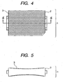
- Fig. 4 is a front view of an optical member of Example 6 according to an embodiment of the present invention.
- an optical member 1 is a concave lens and has a structure in which a transparent antireflection film 3 is provided on a substrate 2.
- the same symbols in other figures as those in Fig. 4 represent the same members.
- Fig. 5 is a sectional view of the optical member of Example 6 taken along the line 5-5 of Fig. 4 .
- the transparent antireflection film 3 having an average surface roughness Ra' of 5 nm or more and a surface area ratio Sr of 1.1 or more, and having a fine irregular structure mainly composed of alumina and containing at least one accessory component selected from the group consisting of zirconia, silica, titania, and zinc oxide was formed on each optical surface.
- the optical surfaces exhibit reduced light reflectance.
- Example 6 describes the case of a concave lens.
- the present invention is not limited thereto, and the lens may be a convex lens or a meniscus lens.
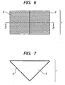
- Fig.6 is a front view of an optical member of Example 7 according to an embodiment of the present invention.
- the optical member 1 is a prism and has a structure in which the transparent antireflection film 3 is provided on the substrate 2.
- Fig. 7 is a sectional view of the optical member of Example 7 taken along the line 7-7 of Fig. 6 .
- the transparent antireflection film 3 having an average surface roughness Ra' of 5 nm or more and a surface area ratio Sr of 1.1 or more, and having a fine irregular structure mainly composed of alumina and containing at least one accessory component selected from the group consisting of zirconia, silica, titania, and zinc oxide was formed on each optical surface.
- the optical surfaces exhibit reduced light reflectance.
- Example 7 describes the case of a prism having optical surfaces of 90° and 45°.
- the present invention is not limited thereto, and the prism may have optical surfaces of any angles.
- Fig. 8 is a front view of an optical member of Example 8 according to an embodiment of the present invention.
- the optical member 1 is a fly-eye integrator and has a structure in which the transparent antireflection film 3 is provided on the substrate 2.
- Fig. 9 is a sectional view of the optical member of Example 8 taken along the line 9-9 of Fig. 8 .
- the transparent antireflection film 3 having an average surface roughness Ra' of 5 nm or more and a surface area ratio Sr of 1.1 or more, having a fine irregular structure mainly composed of alumina and containing at least one accessory component selected from the group consisting of zirconia, silica, titania, and zinc oxide was formed on each optical surface.
- the optical surfaces exhibit reduced light reflectance.
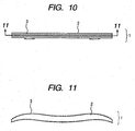
- Fig. 10 is a front view of an optical member of Example 9 according to an embodiment of the present invention.
- the optical member 1 is an f ⁇ lens and has a structure in which the transparent antireflection film 3 is provided on the substrate 2.
- Fig. 11 is a sectional view of the optical member of Example 9 taken along the line 11-11 of Fig. 10 .
- the transparent antireflection film 3 having an average surface roughness Ra' of 5 nm or more and a surface area ratio Sr of 1.1 or more, and having a fine irregular structure mainly composed of alumina and containing at least one accessory component selected from the group consisting of zirconia, silica, titania, and zinc oxide was formed on each optical surface.
- the optical surfaces exhibit reduced light reflectance.
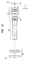
- Example 10 describes an example of the use of an optical member of an embodiment of the present invention for an observation optical system.
- Fig. 12 shows a cross section of an optical system of a pair of optical systems of binoculars.
- reference numeral 124 collectively represents an objective lens forming an observation image
- reference numeral 125 represents a prism (shown developed) for inverting the image
- reference numeral 126 collectively represents an ocular lens
- reference numeral 127 represents an image forming surface
- reference numeral 128 represents a pupil plane (evaluation plane).
- reference numeral 3 (shown as a legend) represents the transparent antireflection film according to an embodiment of the present invention.
- the transparent antireflection film 3 having an average surface roughness Ra' of 5 nm or more and a surface area ratio Sr of 1.1 or more, and having a fine irregular structure mainly composed of alumina and containing at least one accessory component selected from the group consisting of zirconia, silica, titania, and zinc oxide was formed on an optical surface.
- the optical surface exhibits reduced light reflectance.
- the transparent antireflection film 3 having a fine irregular structure was not provided on an optical surface 129 of the objective lens closest to an object and an optical surface 130 of the ocular lens closest to the evaluation plane because performance thereof degrades through contact and the like during use.
- the present invention is not limited thereto, and the transparent antireflection film 3 may be provided on the optical surfaces 129 and 130.
- Example 11 describes an example of the use of an optical member of an embodiment of the present invention for an image pickup optical system.
- Fig. 13 shows a cross section of a shooting lens (telescopic lens) such as a camera.
- a shooting lens telescopic lens
- reference numeral 127 represents a film as an image forming surface, or a solid-state image pickup element (photoelectric conversion element) such as a CCD or a CMOS, and reference numeral 131 represents an iris.
- reference numeral 3 (shown as a legend) represents the transparent antireflection film according to an embodiment of the present invention.
- the transparent antireflection film 3 having an average surface roughness Ra' of 5 nm or more and a surface area ratio Sr of 1.1 or more, and having a fine irregular structure mainly composed of alumina and containing at least one accessory component selected from the group consisting of zirconia, silica, titania, and zinc oxide was formed on an optical surface.
- the optical surface exhibits reduced light reflectance.
- the transparent antireflection film 3 having a fine irregular structure was not provided on the optical surface 129 of the objective lens closest to an object because performance thereof degrades through contact and the like during use.
- the present invention is not limited thereto, and the transparent antireflection film 3 may be provided on the optical surface 129.
- Reference numeral 130 also represents the optical surface of the ocular lens closest to the evaluation plane as that in Fig. 12 .
- Example 12 describes an example of the use of an optical member of an embodiment of the present invention for a projection optical system (projector).
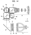
- Fig. 14 shows a cross section of a projector optical system.
- reference numeral 12 represents a light source
- reference numerals 13a and 13b each represent a fly-eye integrator
- reference numeral 14 represents a polarization conversion element
- reference numeral 15 represents a condensing lens
- reference numeral 16 represents a mirror
- reference numeral 17 represents a field lens
- reference numerals 18a, 18b, 18c, and 18d each represent a prism
- reference numerals 19a, 19b, and 19c each represent a light modulation element
- reference numeral 20 collectively represents a projection lens.
- reference numeral 3 (shown as a legend) represents the transparent antireflection film according to an embodiment of the present invention.
- the transparent antireflection film 3 having an average surface roughness Ra' of 5 nm or more and a surface area ratio Sr of 1.1 or more, and having a fine irregular structure mainly composed of alumina and containing at least one accessory component selected from the group consisting of zirconia, silica, titania, and zinc oxide was formed on an optical surface.
- the optical surface exhibits reduced light reflectance.
- the transparent antireflection film 3 of Example 12 is mainly composed of alumina and contains at least one accessory component selected from the group consisting of zirconia, silica, titania, and zinc oxide.
- the transparent antireflection film 3 has high heat resistance and may be used at a position of 13a close to the light source 12 and exposed to high heat without possibility of performance degradation.
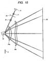
- Example 13 describes an example of the use of an optical member of an embodiment of the present invention for a scanning optical system (laser beam printer).
- Fig. 15 shows a cross section of the scanning optical system.
- reference numeral 12 represents the light source
- reference numeral 21 represents a collimator lens
- reference numeral 25 represents an iris
- reference numeral 22 represents a cylindrical lens
- reference numeral 23 represents a light deflector
- reference numerals 24a and 24b each represent an f ⁇ lens
- reference numeral 26 represents an image surface.
- reference numeral 3 (shown as a legend) represents the transparent antireflection film according to an embodiment of the present invention.
- the transparent antireflection film 3 having an average surface roughness Ra' of 5 nm or more and a surface area ratio of Sr of 1.1 or more, and having a fine irregular structure mainly composed of alumina and containing at least one accessory component selected from the group consisting of zirconia, silica, titania, and zinc oxide was formed on an optical surface.
- the optical surface exhibits reduced light reflectance, and high quality image formation is realized.
- the film and the transparent antireflection film can be applied to an arbitrary transparent base material, and show an excellent antireflection effect for visible light by reducing reflection at an interface between the base material and the irregularities. Therefore, the film and the transparent antireflection film can be used for optical members including: various displays such as a word processor display, a computer display, a TV display, and a plasma display panel; polarizing plates used for liquid crystal display devices; and sunglass lenses, prescription glass lenses, finder lenses for cameras, prisms, fly-eye lenses, toric lenses, and the like, all made of transparent plastics.
- various displays such as a word processor display, a computer display, a TV display, and a plasma display panel
- polarizing plates used for liquid crystal display devices polarizing plates used for liquid crystal display devices
- sunglass lenses prescription glass lenses, finder lenses for cameras, prisms, fly-eye lenses, toric lenses, and the like, all made of transparent plastics.
- the film and the transparent antireflection film can be used for optical members including: various optical lenses employing the aforementioned optical members for an image pickup optical system, an observation optical system such as binoculars, a projection optical system used for a liquid crystal projector or the like, and a scanning optical system used for a laser beam printer or the like; covers for various measuring instruments; and windows of cars, trains, and the like.
Landscapes
- Chemical & Material Sciences (AREA)
- Life Sciences & Earth Sciences (AREA)
- Engineering & Computer Science (AREA)
- Chemical Kinetics & Catalysis (AREA)
- General Chemical & Material Sciences (AREA)
- Geochemistry & Mineralogy (AREA)
- Materials Engineering (AREA)
- Organic Chemistry (AREA)
- Physics & Mathematics (AREA)
- General Physics & Mathematics (AREA)
- Optics & Photonics (AREA)
- Dispersion Chemistry (AREA)
- Composite Materials (AREA)
- Surface Treatment Of Optical Elements (AREA)
- Laminated Bodies (AREA)
- Projection Apparatus (AREA)
- Mechanical Optical Scanning Systems (AREA)
Claims (10)
- Optisches Element, das umfasst:ein Substrat,einen Antireflexionsfilm, der eine auf dem Substrat bereitgestellte Dünnfilmschicht umfasst und auf der Dünnfilmschicht bereitgestellte feine Unregelmäßigkeiten aufweist,wobei die Dünnfilmschicht zumindest eines ausgewählt aus der Gruppe bestehend aus Zirkonoxid, Siliziumoxid, Titanoxid und Zinkoxid enthält,dadurch gekennzeichnet, dass die feinen Unregelmäßigkeiten aus Plattenkristallen gebildet sind, die hauptsächlich aus Aluminiumoxid bestehen, und wobei sich der Brechungsindex zwischen der feinen unregelmäßigen Struktur und dem Substrat kontinuierlich ändert.
- Optisches Element nach Anspruch 1, wobei die feinen Unregelmäßigkeiten, die hauptsächlich aus Aluminiumoxid bestehen, eine Höhe von 0,005 µm bis 5,0 µm aufweisen.
- Optisches Element nach Anspruch 1 oder Anspruch 2, wobei die durchschnittliche Oberflächenrauheit Ra', welche durch flächiges Erstrecken einer Mittelliniendurchschnittsrauheit erhalten ist, des Films mit den feinen Unregelmäßigkeiten, die hauptsächlich aus Aluminiumoxid bestehen, 5 nm oder mehr beträgt; und ein Oberflächenverhältnis Sr = S / S0 des Films 1,1 oder mehr beträgt, vorausgesetzt, dass S0 eine Fläche einer ideal flachen Messoberfläche darstellt, und S eine Oberfläche einer tatsächlichen Messoberfläche darstellt.
- Optisches Element nach einem der Ansprüche 1 bis 3, wobei ein Gehalt zumindest eines ausgewählt aus der Gruppe bestehend aus Zirkonoxid, Siliziumoxid, Titanoxid und Zinkoxid in der Dünnfilmschicht 0,001 oder mehr und weniger als 1,0 im Gewichtsverhältnis bezüglich eines Gewichtes des Films beträgt.
- Optisches Element nach einem der Ansprüche 1 bis 4, wobei die Plattenkristalle hauptsächlich aus Hydroxid von Aluminium oder Hydrat von Aluminiumoxid bestehen.
- Optisches Element nach einem der Ansprüche 1 bis 5, wobei die Dünnfilmschicht einen Brechungsindex zwischen dem Brechungsindex des Substrats und dem Brechungsindex der feinen Unregelmäßigkeiten aufweist.
- Verfahren zum Herstellen eines nach Anspruch 1 definierten optischen Elements, wobei das Verfahren, in Reihenfolge, die Schritte umfasst:Aufbringen einer Lösung, die eine Aluminiumverbindung und zumindest eine Verbindung ausgewählt aus der Gruppe bestehend aus einer Zirkonverbindung, einer Siliziumverbindung, einer Titanverbindung und einer Zinkverbindung enthält, auf das Substrat, um einen Überzug zu bilden; undUnterziehen des Überzugs einer Warmwasserbehandlung, um Plattenkristalle, die hauptsächlich aus Aluminiumoxid bestehen, auf einer Oberfläche des Überzugs abzuscheiden, wodurch der Antireflexionsfilm, der feine Unregelmäßigkeiten und eine unter den Unregelmäßigkeiten gebildete Dünnfilmschicht umfasst, hergestellt wird, wobei die Dünnfilmschicht die Plattenkristalle trägert und ein Oxid umfasst, das zumindest einen Bestandteil ausgewählt aus der Gruppe bestehend aus Zirkonoxid, Siliziumoxid, Titanoxid und Zinkoxid enthält.
- Verfahren nach Anspruch 7, wobei die Lösung durch Mischen einer Lösung, die ein Metallalkoxid oder ein Metallsalz von Aluminium enthält, und einer Lösung, die ein Metallalkoxid oder ein Metallsalz zumindest eines ausgewählt aus der Gruppe bestehend aus Zirkon, Silizium, Titan und Zink enthält, gebildet wird.
- Verfahren nach Anspruch 7 oder Anspruch 8, wobei die Plattenkristalle hauptsächlich aus Hydroxid von Aluminium oder Hydrat von Aluminiumoxid bestehen.
- Verfahren nach einem der Ansprüche 7 bis 9, wobei die Dünnfilmschicht einem Brechungsindex zwischen dem Brechungsindex des Substrats und dem Brechungsindex der feinen Unregelmäßigkeiten aufweist.
Applications Claiming Priority (4)
| Application Number | Priority Date | Filing Date | Title |
|---|---|---|---|
| JP2004046257 | 2004-02-23 | ||
| JP2004046257 | 2004-02-23 | ||
| JP2005006760A JP4182236B2 (ja) | 2004-02-23 | 2005-01-13 | 光学部材および光学部材の製造方法 |
| JP2005006760 | 2005-01-13 |
Publications (2)
| Publication Number | Publication Date |
|---|---|
| EP1574881A1 EP1574881A1 (de) | 2005-09-14 |
| EP1574881B1 true EP1574881B1 (de) | 2010-06-30 |
Family
ID=34829483
Family Applications (1)
| Application Number | Title | Priority Date | Filing Date |
|---|---|---|---|
| EP05250988A Expired - Fee Related EP1574881B1 (de) | 2004-02-23 | 2005-02-22 | Optisches Element mit Antireflexfilm mit feinen Oberflächen-Unebenheiten, dessen Herstellungsverfahren |
Country Status (5)
| Country | Link |
|---|---|
| US (2) | US20050233113A1 (de) |
| EP (1) | EP1574881B1 (de) |
| JP (1) | JP4182236B2 (de) |
| CN (2) | CN100343697C (de) |
| DE (1) | DE602005022006D1 (de) |
Families Citing this family (66)
| Publication number | Priority date | Publication date | Assignee | Title |
|---|---|---|---|---|
| US8501270B2 (en) * | 2005-02-18 | 2013-08-06 | Canon Kabushiki Kaisha | Optical transparent member and optical system using the same |
| JP4520418B2 (ja) * | 2005-02-18 | 2010-08-04 | キヤノン株式会社 | 光学用透明部材及びそれを用いた光学系 |
| JP4790396B2 (ja) * | 2005-12-02 | 2011-10-12 | 学校法人東京理科大学 | 透明膜の製造方法 |
| KR100757229B1 (ko) * | 2005-12-05 | 2007-09-10 | 한국전자통신연구원 | 리눅스 시스템상에서 usb 디바이스 드라이버 개발을지원하는 운영체제 자원 진단 장치 및 방법 |
| JP2007183366A (ja) | 2006-01-05 | 2007-07-19 | Pentax Corp | 防塵性光透過性部材及びその用途、並びにその部材を具備する撮像装置 |
| TW200746123A (en) | 2006-01-11 | 2007-12-16 | Pentax Corp | Optical element having anti-reflection coating |
| EP1873126A1 (de) * | 2006-02-22 | 2008-01-02 | Central Glass Co., Ltd. | Blendfreies Glassubstrat |
| JP5016872B2 (ja) * | 2006-08-30 | 2012-09-05 | キヤノン電子株式会社 | 光学フィルタ |
| JP5060091B2 (ja) * | 2006-09-21 | 2012-10-31 | 三菱電線工業株式会社 | 多孔性薄膜の製造方法、及び多孔性薄膜を備えた光学部材の製造方法 |
| JP5049549B2 (ja) * | 2006-10-25 | 2012-10-17 | キヤノン株式会社 | 質量分析用基板、その製造方法および質量分析測定装置 |
| JP4747078B2 (ja) * | 2006-11-17 | 2011-08-10 | Necディスプレイソリューションズ株式会社 | 偏光変換素子および投写型表示装置 |
| EP1947486B9 (de) * | 2007-01-22 | 2012-03-14 | Canon Kabushiki Kaisha | Optisches Bauteil mit Antireflexbeschichtung und Herstellungsverfahren dafür |
| JP4639241B2 (ja) * | 2007-02-20 | 2011-02-23 | キヤノン株式会社 | 光学用部材、それを用いた光学系及び光学用部材の製造方法 |
| US20080198457A1 (en) * | 2007-02-20 | 2008-08-21 | Pentax Corporation | Dust-proof, reflecting mirror and optical apparatus comprising same |
| JP5535052B2 (ja) * | 2007-02-20 | 2014-07-02 | キヤノン株式会社 | 光学用部材、それを用いた光学系 |
| KR100912260B1 (ko) * | 2007-03-28 | 2009-08-17 | 제일모직주식회사 | 표면에 일정 조도를 갖는 액정표시장치용 광학 프리즘 시트 |
| EP2000289A3 (de) * | 2007-06-06 | 2016-04-06 | Canon Kabushiki Kaisha | Verfahren zur Herstellung eines optischen Elements und optisches Element |
| JP5279344B2 (ja) * | 2007-06-06 | 2013-09-04 | キヤノン株式会社 | 光学素子の製造方法 |
| JP5213424B2 (ja) * | 2007-12-10 | 2013-06-19 | キヤノン株式会社 | 光学系及びそれを有する光学機器 |
| GB0803702D0 (en) | 2008-02-28 | 2008-04-09 | Isis Innovation | Transparent conducting oxides |
| KR20090108853A (ko) * | 2008-04-14 | 2009-10-19 | 삼성전자주식회사 | 무기물 패턴 형성용 조성물 및 그를 이용한 무기물패턴형성 방법 |
| JP5777682B2 (ja) * | 2008-08-29 | 2015-09-09 | キヤノン株式会社 | 光学素子及びその製造方法、光学系、光学機器 |
| JP5511258B2 (ja) | 2008-08-29 | 2014-06-04 | キヤノン株式会社 | 光学素子及び光学系 |
| JP5311944B2 (ja) * | 2008-09-12 | 2013-10-09 | キヤノン株式会社 | 光学素子及びそれを有する光学系 |
| JP2010072046A (ja) * | 2008-09-16 | 2010-04-02 | Canon Inc | 光学素子及びそれを有する光学装置 |
| EP2372404B1 (de) | 2008-10-17 | 2013-01-16 | Carl Zeiss SMT GmbH | Projektionsobjektiv mit hoher Transmission und hoher Apertur sowie Projektionsbelichtungsvorrichtung |
| FR2938931B1 (fr) | 2008-11-27 | 2011-03-18 | Essilor Int | Procede de fabrication d'un article d'optique a proprietes antireflets |
| GB0915376D0 (en) | 2009-09-03 | 2009-10-07 | Isis Innovation | Transparent conducting oxides |
| JP5511307B2 (ja) | 2009-10-23 | 2014-06-04 | キヤノン株式会社 | 光学部材、及びその製造方法 |
| CN102666941B (zh) * | 2009-11-06 | 2015-01-21 | 夏普株式会社 | 模具的制造方法和模具 |
| JP5279858B2 (ja) | 2010-05-07 | 2013-09-04 | キヤノン株式会社 | 酸化アルミニウム前駆体ゾル、および光学用部材の製造方法 |
| JP2012073590A (ja) | 2010-08-31 | 2012-04-12 | Canon Inc | 光学部材、その製造方法及び光学系 |
| JP6080349B2 (ja) * | 2010-11-26 | 2017-02-15 | キヤノン株式会社 | 光学部材および撮像装置 |
| US20120207973A1 (en) | 2011-02-15 | 2012-08-16 | Canon Kabushiki Kaisha | Optical member, method of manufacturing the same, and optical system using the same |
| JP5647924B2 (ja) * | 2011-03-18 | 2015-01-07 | 富士フイルム株式会社 | 光学部材の製造方法 |
| JP5839870B2 (ja) | 2011-07-15 | 2016-01-06 | キヤノン株式会社 | 光学素子および光学素子の製造方法 |
| EP2645136B1 (de) | 2012-03-29 | 2017-01-18 | Canon Kabushiki Kaisha | Optisches Element mit texturierter Struktur und Verfahren zu dessen Herstellung |
| EP2644661B1 (de) | 2012-03-29 | 2018-12-05 | Canon Kabushiki Kaisha | Vorläufer-sol von aluminiumoxid und verfahren zur herstellung davon, verfahren zur herstellung eines optischen elements, optisches element, und optisches system |
| JP5950667B2 (ja) | 2012-04-16 | 2016-07-13 | キヤノン株式会社 | 光学用部材、その製造方法および光学用部材の光学膜 |
| KR102138638B1 (ko) * | 2012-04-27 | 2020-07-28 | 오사카 리서치 인스티튜트 오브 인더스트리얼 사이언스 앤드 테크놀러지 | 금속 산화물 분산체, 금속 산화물 분산체 함유 중합성 조성물, 및 이의 중합물 |
| JP6071318B2 (ja) | 2012-08-09 | 2017-02-01 | キヤノン株式会社 | 光学部材および光学部材の製造方法 |
| JP6080299B2 (ja) | 2013-03-15 | 2017-02-15 | 富士フイルム株式会社 | 光学部材およびその製造方法 |
| KR101531809B1 (ko) * | 2013-03-27 | 2015-06-25 | 엔지케이 인슐레이터 엘티디 | 반도체용 복합 기판의 핸들 기판 |
| US9359249B2 (en) * | 2013-05-29 | 2016-06-07 | Guardian Industries Corp. | Anti-corrosion anti-reflection glass and related methods |
| EP3006225A4 (de) * | 2013-05-31 | 2017-01-11 | Toppan Printing Co., Ltd. | Schichtmedium für übertragung und drucksache |
| JP6396003B2 (ja) | 2013-06-03 | 2018-09-26 | 富士フイルム株式会社 | 反射防止膜を備えた光学部材 |
| JP6468696B2 (ja) * | 2013-06-21 | 2019-02-13 | キヤノン株式会社 | 光学用部材およびその製造方法 |
| JP6795877B2 (ja) * | 2013-12-25 | 2020-12-02 | 東京応化工業株式会社 | 表面被覆膜の形成方法及び表面被覆膜を有する太陽電池 |
| JP6234857B2 (ja) | 2014-03-24 | 2017-11-22 | 富士フイルム株式会社 | 反射防止機能付きレンズの製造方法 |
| WO2016136261A1 (ja) | 2015-02-27 | 2016-09-01 | 富士フイルム株式会社 | 反射防止膜および光学部材 |
| JP6692342B2 (ja) | 2015-02-27 | 2020-05-13 | 富士フイルム株式会社 | 反射防止膜およびその製造方法、並びに光学部材 |
| WO2016159290A1 (ja) | 2015-03-31 | 2016-10-06 | 富士フイルム株式会社 | 反射防止膜及びその製造方法 |
| JP6266840B2 (ja) * | 2015-04-20 | 2018-01-24 | 富士フイルム株式会社 | 構造物の製造方法 |
| CN105463549B (zh) * | 2015-12-03 | 2018-06-26 | 中国航空工业集团公司北京航空材料研究院 | 一种提高铝及铝合金防护性能的阳极化方法 |
| JP6923998B2 (ja) | 2016-03-24 | 2021-08-25 | キヤノン株式会社 | 光学部材およびその製造方法 |
| JP6786248B2 (ja) | 2016-04-12 | 2020-11-18 | キヤノン株式会社 | 光学素子およびその製造方法 |
| JP6971587B2 (ja) | 2017-02-27 | 2021-11-24 | キヤノン株式会社 | 光学素子及びその製造方法、光学機器 |
| CN109196388A (zh) | 2017-03-13 | 2019-01-11 | 京东方科技集团股份有限公司 | 抗反射涂层、触控基板、显示装置和制造抗反射涂层的方法 |
| US10920139B2 (en) * | 2017-06-30 | 2021-02-16 | Sharp Kabushiki Kaisha | Phosphor layer composition, phosphor member, light source device, and projection device |
| US11105960B2 (en) | 2017-12-19 | 2021-08-31 | Canon Kabushiki Kaisha | Optical element and method of producing the element, and optical instrument |
| CN108342683A (zh) * | 2018-02-09 | 2018-07-31 | 京东方科技集团股份有限公司 | 一种预溅射基板及其制作方法 |
| JP7065995B2 (ja) * | 2018-09-27 | 2022-05-12 | 富士フイルム株式会社 | 反射防止膜の製造方法、および微細凹凸構造の形成方法 |
| US20230003994A1 (en) * | 2019-12-04 | 2023-01-05 | Sharp Kabushiki Kaisha | Wavelength conversion element, wavelength conversion device, and light-emission system |
| US11714212B1 (en) * | 2020-09-14 | 2023-08-01 | Apple Inc. | Conformal optical coatings for non-planar substrates |
| CN114690291A (zh) * | 2022-04-15 | 2022-07-01 | 苏州锦乐美新材料有限公司 | 一种高辉度抗刮复合光学膜片及其制备方法 |
| TW202344914A (zh) * | 2022-05-13 | 2023-11-16 | 大立光電股份有限公司 | 成像鏡頭、相機模組及電子裝置 |
Family Cites Families (23)
| Publication number | Priority date | Publication date | Assignee | Title |
|---|---|---|---|---|
| US4252843A (en) * | 1977-02-18 | 1981-02-24 | Minnesota Mining And Manufacturing Company | Process for forming a microstructured transmission and reflectance modifying coating |
| US4199322A (en) * | 1978-08-17 | 1980-04-22 | The United States Of America As Represented By The Secretary Of Agriculture | Antibacterial textile finishes utilizing zinc acetate and hydrogen peroxide |
| US4645337A (en) * | 1984-10-31 | 1987-02-24 | Ppg Industries, Inc. | System for detecting variations in surface composition of an article |
| CA1275208C (en) * | 1985-01-25 | 1990-10-16 | Roger W. Lange | Silica coating |
| JPH0729902B2 (ja) * | 1985-07-11 | 1995-04-05 | 住友化学工業株式会社 | メ−クアツプ化粧料 |
| US4830879A (en) * | 1986-09-25 | 1989-05-16 | Battelle Memorial Institute | Broadband antireflective coating composition and method |
| EP0533030B1 (de) * | 1991-09-20 | 1995-06-21 | Hitachi, Ltd. | Verfahren und Vorrichtung für Herstellung einer Antireflektionsbeschichtung einer Kathodenstrahlröhre |
| JP2716330B2 (ja) * | 1992-11-13 | 1998-02-18 | セントラル硝子株式会社 | 低反射ガラスおよびその製法 |
| FR2736632B1 (fr) * | 1995-07-12 | 1997-10-24 | Saint Gobain Vitrage | Vitrage muni d'une couche conductrice et/ou bas-emissive |
| US5948482A (en) * | 1995-09-19 | 1999-09-07 | University Of New Mexico | Ambient pressure process for preparing aerogel thin films reliquified sols useful in preparing aerogel thin films |
| US5948481A (en) * | 1996-11-12 | 1999-09-07 | Yazaki Corporation | Process for making a optical transparency having a diffuse antireflection coating |
| CA2285944A1 (en) * | 1997-04-10 | 1998-10-15 | Corning Incorporated | Optical article with anti-reflecting coating, corresponding coating material and coating method |
| US20010036897A1 (en) * | 1997-12-10 | 2001-11-01 | Kazuya Tsujimichi | Photocatalytic hydrophilifiable material |
| JP3781888B2 (ja) * | 1998-02-13 | 2006-05-31 | 日産自動車株式会社 | 親水性基材およびその製造方法 |
| JP4247354B2 (ja) * | 1999-07-08 | 2009-04-02 | 財団法人大阪産業振興機構 | 表面微細凹凸組織の低温形成法および当該組織を有する基体 |
| JP2001042125A (ja) * | 1999-08-04 | 2001-02-16 | Nitto Denko Corp | 偏光部材、光学部材及び液晶表示装置 |
| US6791649B1 (en) * | 1999-09-28 | 2004-09-14 | Fuji Photo Film Co., Ltd. | Anti-reflection film, polarizing plate comprising the same, and image display device using the anti-reflection film or the polarizing plate |
| US6534176B2 (en) * | 1999-12-10 | 2003-03-18 | Asahi Glass Company, Limited | Scaly silica particles and hardenable composition containing them |
| JP2001254030A (ja) * | 2000-03-13 | 2001-09-18 | Sekisui Jushi Co Ltd | 超撥水性を有する被覆物及びその製造方法 |
| JP2001259521A (ja) * | 2000-03-21 | 2001-09-25 | Dainippon Ink & Chem Inc | 親水性皮膜の形成方法、および、塗装物品 |
| JP2002182003A (ja) * | 2000-12-14 | 2002-06-26 | Canon Inc | 反射防止機能素子、光学素子、光学系および光学機器 |
| WO2003044572A1 (fr) * | 2001-11-22 | 2003-05-30 | Takiron Co., Ltd. | Plaque diffuseur de lumiere |
| JP4094331B2 (ja) * | 2002-04-23 | 2008-06-04 | 川崎重工業株式会社 | 親水性コーティング組成物の製造方法 |
-
2005
- 2005-01-13 JP JP2005006760A patent/JP4182236B2/ja not_active Expired - Fee Related
- 2005-02-16 US US11/058,193 patent/US20050233113A1/en not_active Abandoned
- 2005-02-22 DE DE602005022006T patent/DE602005022006D1/de active Active
- 2005-02-22 EP EP05250988A patent/EP1574881B1/de not_active Expired - Fee Related
- 2005-02-23 CN CNB2005100519955A patent/CN100343697C/zh not_active Expired - Fee Related
- 2005-02-23 CN CN2007101417017A patent/CN101105542B/zh not_active Expired - Fee Related
-
2008
- 2008-09-24 US US12/236,805 patent/US20090022954A1/en not_active Abandoned
Also Published As
| Publication number | Publication date |
|---|---|
| US20090022954A1 (en) | 2009-01-22 |
| DE602005022006D1 (de) | 2010-08-12 |
| CN101105542B (zh) | 2012-08-22 |
| CN1661398A (zh) | 2005-08-31 |
| CN101105542A (zh) | 2008-01-16 |
| CN100343697C (zh) | 2007-10-17 |
| JP2005275372A (ja) | 2005-10-06 |
| EP1574881A1 (de) | 2005-09-14 |
| US20050233113A1 (en) | 2005-10-20 |
| JP4182236B2 (ja) | 2008-11-19 |
Similar Documents
| Publication | Publication Date | Title |
|---|---|---|
| EP1574881B1 (de) | Optisches Element mit Antireflexfilm mit feinen Oberflächen-Unebenheiten, dessen Herstellungsverfahren | |
| EP1693689B1 (de) | Optisches transparentes Element und optisches System damit | |
| US10459125B2 (en) | Optical member, method for manufacturing optical member, and optical film of optical member | |
| EP2582764B1 (de) | Anorganische oxidbeschichtung | |
| US8603372B2 (en) | Method of manufacturing optical element, and optical element | |
| US8623312B2 (en) | Process for producing dispersion of hollow fine SiO2 particles, coating composition and substrate with antireflection coating film | |
| CN100595608C (zh) | 光学透明部件和使用该光学透明部件的光学系统 | |
| EP2696221A1 (de) | Optisches Element und Verfahren zur Herstellung einer optischen Vorrichtung | |
| CN101324676A (zh) | 制造光学元件的方法和光学元件 | |
| JP4488764B2 (ja) | 透明反射防止膜、その製造方法および光学部材 | |
| US8501270B2 (en) | Optical transparent member and optical system using the same | |
| JP2009163228A (ja) | 酸化物膜、酸化物膜形成用塗布液、酸化物膜を用いた光学部材、およびそれらの製造方法 |
Legal Events
| Date | Code | Title | Description |
|---|---|---|---|
| PUAI | Public reference made under article 153(3) epc to a published international application that has entered the european phase |
Free format text: ORIGINAL CODE: 0009012 |
|
| AK | Designated contracting states |
Kind code of ref document: A1 Designated state(s): AT BE BG CH CY CZ DE DK EE ES FI FR GB GR HU IE IS IT LI LT LU MC NL PL PT RO SE SI SK TR |
|
| AX | Request for extension of the european patent |
Extension state: AL BA HR LV MK YU |
|
| AKX | Designation fees paid |
Designated state(s): DE FR GB |
|
| 17P | Request for examination filed |
Effective date: 20060606 |
|
| RAP1 | Party data changed (applicant data changed or rights of an application transferred) |
Owner name: OSAKA PREFECTURE UNIVERSITY Owner name: CANON KABUSHIKI KAISHA |
|
| 17Q | First examination report despatched |
Effective date: 20081024 |
|
| RTI1 | Title (correction) |
Free format text: OPTICAL MEMBER WITH AN ANTIREFLECTION FILM HAVING FINE IRREGULARITIES ON THE SURFACE, PRODUCTION METHOD FOR THE SAME |
|
| GRAP | Despatch of communication of intention to grant a patent |
Free format text: ORIGINAL CODE: EPIDOSNIGR1 |
|
| GRAS | Grant fee paid |
Free format text: ORIGINAL CODE: EPIDOSNIGR3 |
|
| GRAA | (expected) grant |
Free format text: ORIGINAL CODE: 0009210 |
|
| AK | Designated contracting states |
Kind code of ref document: B1 Designated state(s): DE FR GB |
|
| REG | Reference to a national code |
Ref country code: GB Ref legal event code: FG4D |
|
| REF | Corresponds to: |
Ref document number: 602005022006 Country of ref document: DE Date of ref document: 20100812 Kind code of ref document: P |
|
| PLBE | No opposition filed within time limit |
Free format text: ORIGINAL CODE: 0009261 |
|
| STAA | Information on the status of an ep patent application or granted ep patent |
Free format text: STATUS: NO OPPOSITION FILED WITHIN TIME LIMIT |
|
| 26N | No opposition filed |
Effective date: 20110331 |
|
| REG | Reference to a national code |
Ref country code: DE Ref legal event code: R097 Ref document number: 602005022006 Country of ref document: DE Effective date: 20110330 |
|
| REG | Reference to a national code |
Ref country code: FR Ref legal event code: PLFP Year of fee payment: 12 |
|
| REG | Reference to a national code |
Ref country code: FR Ref legal event code: PLFP Year of fee payment: 13 |
|
| REG | Reference to a national code |
Ref country code: FR Ref legal event code: PLFP Year of fee payment: 14 |
|
| PGFP | Annual fee paid to national office [announced via postgrant information from national office to epo] |
Ref country code: FR Payment date: 20210120 Year of fee payment: 17 |
|
| PGFP | Annual fee paid to national office [announced via postgrant information from national office to epo] |
Ref country code: GB Payment date: 20210120 Year of fee payment: 17 Ref country code: DE Payment date: 20210120 Year of fee payment: 17 |
|
| REG | Reference to a national code |
Ref country code: DE Ref legal event code: R119 Ref document number: 602005022006 Country of ref document: DE |
|
| GBPC | Gb: european patent ceased through non-payment of renewal fee |
Effective date: 20220222 |
|
| PG25 | Lapsed in a contracting state [announced via postgrant information from national office to epo] |
Ref country code: FR Free format text: LAPSE BECAUSE OF NON-PAYMENT OF DUE FEES Effective date: 20220228 |
|
| PG25 | Lapsed in a contracting state [announced via postgrant information from national office to epo] |
Ref country code: GB Free format text: LAPSE BECAUSE OF NON-PAYMENT OF DUE FEES Effective date: 20220222 Ref country code: DE Free format text: LAPSE BECAUSE OF NON-PAYMENT OF DUE FEES Effective date: 20220901 |