EP1567302B1 - Ajustage au laser de resistances - Google Patents
Ajustage au laser de resistances Download PDFInfo
- Publication number
- EP1567302B1 EP1567302B1 EP03783744A EP03783744A EP1567302B1 EP 1567302 B1 EP1567302 B1 EP 1567302B1 EP 03783744 A EP03783744 A EP 03783744A EP 03783744 A EP03783744 A EP 03783744A EP 1567302 B1 EP1567302 B1 EP 1567302B1
- Authority
- EP
- European Patent Office
- Prior art keywords
- trim
- laser
- resistors
- resistor
- bin
- Prior art date
- Legal status (The legal status is an assumption and is not a legal conclusion. Google has not performed a legal analysis and makes no representation as to the accuracy of the status listed.)
- Expired - Lifetime
Links
Images


Classifications
-
- H—ELECTRICITY
- H05—ELECTRIC TECHNIQUES NOT OTHERWISE PROVIDED FOR
- H05K—PRINTED CIRCUITS; CASINGS OR CONSTRUCTIONAL DETAILS OF ELECTRIC APPARATUS; MANUFACTURE OF ASSEMBLAGES OF ELECTRICAL COMPONENTS
- H05K1/00—Printed circuits
- H05K1/16—Printed circuits incorporating printed electric components, e.g. printed resistors, capacitors or inductors
- H05K1/167—Printed circuits incorporating printed electric components, e.g. printed resistors, capacitors or inductors incorporating printed resistors
-
- B—PERFORMING OPERATIONS; TRANSPORTING
- B23—MACHINE TOOLS; METAL-WORKING NOT OTHERWISE PROVIDED FOR
- B23K—SOLDERING OR UNSOLDERING; WELDING; CLADDING OR PLATING BY SOLDERING OR WELDING; CUTTING BY APPLYING HEAT LOCALLY, e.g. FLAME CUTTING; WORKING BY LASER BEAM
- B23K26/00—Working by laser beam, e.g. welding, cutting or boring
- B23K26/351—Working by laser beam, e.g. welding, cutting or boring for trimming or tuning of electrical components
-
- H—ELECTRICITY
- H01—ELECTRIC ELEMENTS
- H01C—RESISTORS
- H01C17/00—Apparatus or processes specially adapted for manufacturing resistors
- H01C17/22—Apparatus or processes specially adapted for manufacturing resistors adapted for trimming
- H01C17/24—Apparatus or processes specially adapted for manufacturing resistors adapted for trimming by removing or adding resistive material
- H01C17/242—Apparatus or processes specially adapted for manufacturing resistors adapted for trimming by removing or adding resistive material by laser
-
- H—ELECTRICITY
- H05—ELECTRIC TECHNIQUES NOT OTHERWISE PROVIDED FOR
- H05K—PRINTED CIRCUITS; CASINGS OR CONSTRUCTIONAL DETAILS OF ELECTRIC APPARATUS; MANUFACTURE OF ASSEMBLAGES OF ELECTRICAL COMPONENTS
- H05K1/00—Printed circuits
- H05K1/02—Details
- H05K1/11—Printed elements for providing electric connections to or between printed circuits
- H05K1/115—Via connections; Lands around holes or via connections
- H05K1/116—Lands, clearance holes or other lay-out details concerning the surrounding of a via
-
- H—ELECTRICITY
- H05—ELECTRIC TECHNIQUES NOT OTHERWISE PROVIDED FOR
- H05K—PRINTED CIRCUITS; CASINGS OR CONSTRUCTIONAL DETAILS OF ELECTRIC APPARATUS; MANUFACTURE OF ASSEMBLAGES OF ELECTRICAL COMPONENTS
- H05K2203/00—Indexing scheme relating to apparatus or processes for manufacturing printed circuits covered by H05K3/00
- H05K2203/17—Post-manufacturing processes
- H05K2203/171—Tuning, e.g. by trimming of printed components or high frequency circuits
-
- H—ELECTRICITY
- H05—ELECTRIC TECHNIQUES NOT OTHERWISE PROVIDED FOR
- H05K—PRINTED CIRCUITS; CASINGS OR CONSTRUCTIONAL DETAILS OF ELECTRIC APPARATUS; MANUFACTURE OF ASSEMBLAGES OF ELECTRICAL COMPONENTS
- H05K3/00—Apparatus or processes for manufacturing printed circuits
- H05K3/02—Apparatus or processes for manufacturing printed circuits in which the conductive material is applied to the surface of the insulating support and is thereafter removed from such areas of the surface which are not intended for current conducting or shielding
- H05K3/027—Apparatus or processes for manufacturing printed circuits in which the conductive material is applied to the surface of the insulating support and is thereafter removed from such areas of the surface which are not intended for current conducting or shielding the conductive material being removed by irradiation, e.g. by photons, alpha or beta particles
Definitions
- the present invention generally relates to fabrication of electronic circuit elements, and more particularly, to systems and methods for laser trimming of passive components fabricated on a substrate layer.
- Resistors fabricated on substrate layers offer significant electrical performance advantages over surface mount resistors.
- the problem is that printed circuit board and other circuit substrate manufacturers must fabricate these resistors on the substrate layer with the desired nominal and tolerance values at the time the substrate layer is being manufactured. Because printed resistors are typically buried within a printed circuit board or other circuit platform under one or more lamination layers, the platform manufacturer is generally unable to correct defects at a later time. The need to properly fabricate resistors the first time for both nominal and tolerance values has been an inhibiting factor for high yield and high volume buried resistor processes. These problems have become especially apparent for printed circuit boards having resistors printed on multiple layers. If resistors at one layer fail to meet the required specifications, the entire circuit board may be defective. As a result, multi-layered printed circuit boards and other circuit platforms such as multi-chip modules, hybrid circuits and chip packages typically suffer from exceptionally low yields.
- US 5,443,534 discloses the manufacture on a production line of electronic components for connection in electronic circuits. Operating parameters of a laser are determined automatically for use in trimming resistor blanks belonging to a common batch of blanks.
- GB 2,038,562 discloses a method of obtaining a desired resistance between two locations on a layer of resistive material that includes the step of removing the material from the layer over a convoluted path which surrounds one of the locations to define a resistive path of sufficient length along the layer to obtain the desired resistance.
- the invention refers to a method for laser trimming resistors according to claim 1 and to a trim application for trimming resistors according to claim 9. Embodiments of the invention are defined in the dependent claims.
- Embodiments of the present invention alleviate many of the foregoing problems by providing improved systems and methods for laser trimming of passive components.
- a resistance value for each resistor printed on a substrate layer is measured.
- the resistors are then sorted into one or more bins based on the measured resistance value and target resistance value associated with each annular resistor.
- a laser trim file is assigned to each bin using a predictive trim formulation, where each laser trim file defines a set of configuration parameters for a laser drill to conform each resistor to their respective target value.
- a laser drill may then be used to trim the resistors within each bin in accordance with the laser trim file assigned to that bin.
- the laser trim file may define a drill pattern on the resistor to form a planar channel within the resistor.
- the laser drill file may include a laser beam step size, an overlap factor and number of feed steps across the resistor that causes the laser drill to form a planar channel of the desired shape and depth.
- a trim application may also be used to display a distribution of the trimmed resistance values and other statistical information to determine the performance of the laser drill file associated with particular bins. This statistical information may be used by the circuit substrate manufacturer to adjust the parameters of the laser drill files.
- the statistical information provided by the laser trim application may also enhance the performance of laser trimming and increase circuit board yields by providing sufficient information regarding the laser trimming process or underlying print screen process to enable the manufacturer to take appropriate action.
- Embodiments of the present invention provide systems and methods for laser trimming of passive components on a-circuit-substrate layers, such as annular passive components on a printed circuit board.
- a-circuit-substrate layers such as annular passive components on a printed circuit board.
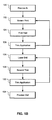
- the exemplary system includes a screen printer 110, a resistance tester 112, a trim application 114 and a laser drill 116.
- the resistance tester 112 In operation, printed circuit boards or other substrate layers with fabricated resistors using the screen printer 110 are provided to the resistance tester 112, which probes each resistor on the printed circuit board and measures the associated resistance.
- the resistance tester 112 outputs a file that provides the location (x, y coordinates) of each resistor and the associated resistance value.
- the trim application 114 uses the output of the resistance tester 112 to generate a screen printing report. As will be discussed in further detail in connection with Figure 2 , this report may be configured to display a distribution of the measured resistance values and other statistical information that may then be used to adjust the processes used by the screen printer 110.
- a circuit substrate layer comprises a composite plane layer consisting of one or more conductive layers (such as copper) laminated or bonded to a dielectric layer.
- the circuit substrate layer typically consist of two conductive layers bonded to both sides of a dielectric layer.
- a multi-layer printed circuit board includes multiple circuit substrate layers.
- the dielectric layer can be reinforced such as with FR-406 glass-resin systems according to an embodiment. Alternatively the dielectric layer may be non-reinforced such as in the case of capton, teflon, or polyamide.
- One embodiment of the circuit substrate layer consists of a 0.05mm (0.002") thick FR-406 dielectric layer with 14g (1/2 oz) (0.02mm (0.0008" thick)) copper foil bonded to each side of the dielectric.
- the trim application 114 may also be configured to sort the resistors into one or more bins based on the measured resistance value and target resistance value. For example, the trim application 114 may be configured to divide a range of resistance values into a plurality of bins having a predetermined step size (e. g. 0.5 ohms). For resistors having the same target value, the trim application 114 uses the measured resistance value for these resistors to place the resistors in the appropriate bin. The trim application 114 then assigns a laser drill file to each bin based on a predictive trim formulation in order to conform the resistors within each bin to the target resistance value for that bin.
- a predetermined step size e. g. 0.5 ohms
- Each drill file uses knowledge of the resistor material and geometry to define a set of control parameters for the laser drill 116, such as laser beam spot size, pulse duration, energy level, aperture, angle, etc. , that will be used to control the laser drill 116 to adjust the resistors within each bin.
- the laser drill file uses a predictive trim methodology to determine the amount of material to trim and the trim pattern that will predictively change the actual resistor value to conform with the target resistor value.
- the trimmed circuit substrate layer may then be provided to the resistance tester 112 to perform a second resistor test of the circuit substrate layer.
- the resistance tester 112 then generates a yield report that provides information regarding whether particular circuit boards passed predefined pass/fail criteria.
- the measured resistance values for the trimmed resistors may also be provided to the trim application 114 in order to display a distribution of the measured resistance values and other statistical information regarding the performance of laser drill files associated with selected bins. As will be discussed in further detail below, this information may be used to adjust trim tool files associated with particular bins in order to fine tune the performance of particular laser drill files.
- FIG. 1B illustrates a flow diagram of an exemplary system and in accordance with one embodiment of the invention.
- the process flow is shown as part of a larger process flow of processing a printed circuit board or substrate layers in a fabrication process. Preceding steps of the process are shown generally as block 120.
- a screen print operation is performed (block 122).
- Resistors are printed on a printed circuit board or other substrate layer using a screen printer.
- the resistors are tested in a first test operation (block 124).
- a trim application runs (block 126).
- the trim operation includes, according to one embodiment, loading and analyzing the test data with resistance values, configuring a tool set, mapping resistors to drill tools and formatting a file to be provided to a laser drill.
- the trim files are mapped to respective sets of resistors and a file embodying the respective commands for the laser drill is formatted.
- Information regarding the resistance values can be used in later screen print operations for the purpose of process improvement, as shown with the connection from block 126 to 122.
- the laser drill operates based on information provided by trim application (block 128).
- the resistors are trimmed according to the drill tools that have been mapped to the respective resistors.
- an additional, second test is performed on the resistors (block 130).
- the trim application runs again based on information on the second test' (block 132). In such operation, the trim application loads and analyzes resistance data collected in the second test. Additional laser trimming may be performed based on such measurements.
- the resulting materials are provided for further processing (block 134).
- Information regarding the resistance values received from the first or second tests can be used in later laser drill operations for the purpose of process improvement, as shown with the connection from block 132 to 128.
- Figure 1C illustrates a block diagram of an exemplary system including details of a trim application in accordance with one embodiment of the invention.
- the system shown generally in Figure 1C includes tester 150, trim application 152, a library of trim files 154 and laser drill 156.
- Trim application 152 includes resistance values 158, sort module 160, assign module 162 and assignment file 164.
- Assignment file 164 includes bins 166 such as bins 168, 170,172, 174 and trim file designation 176 such as trim file designation 178, 180,182 and 184.
- Trim files 154 include files such as 186,188, and 190. Each file contains parameters such as parameters 192, which includes exemplary parameters 194,196, 198.
- the laser trim files can comprise an excellon format.
- Trim application 152 is configured to receive input from tester 150 and provide assignment information to laser drill 156.
- Laser drill 156 also receives trim files 154.
- Trim application 152 receives resistance values 158 from tester 154 for the respective resistors tested. Resistor values 158 in trim application 152 are provided to sort module 160, the result of which is provided to assign module 162.
- Assign module 162 outputs assignment file 164. Resistors are sorted based on resistant values into various bins. Then, different trim files are assigned to respective bins by assign module 162, which creates a file containing the assignment 165 between bins 166 and respective trim file designation 176.
- Assignment file 164 and trim files 154 are uploaded to laser drill 156, which performs drilling operations on the respective resistors based on the assigned file and assigned trim files.
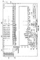
- an exemplary trim tool assignment interface for the trim application in accordance with one embodiment of the present invention is illustrated generally at 200.
- the exemplary interface is intended to provide graphical and statistical information that allows the user to quickly view both screen printing and laser trimming process control.
- the exemplary interface of Figure 2A is shown displaying exemplary data for a 1200 resistor test substrate layer for circuit images after screen printing.
- the sorted resistance data is displayed numerically by image 210 and by resistance bin 220.
- the bin resolution is 0.05 ohm and has a start channel of 0.15 ohm and an end channel of 1.15 ohm.
- Pass/fail results are displayed by image for both mean value (A) and distribution (D) in the upper left corner of the display as illustrated generally at 230, with a total pass per core calculated and displayed at 240.
- the upper and lower tolerance values for the resistor core are also illustrated by upper and lower lines shown generally at 290.
- the user controls the application using the command buttons and numerical inputs at the bottom of the display.
- the number of images per core and the number of resistors per image are first input into the trim application at the bottom of the display as illustrated generally at 250.
- the user can then load data into the trim application using the load buttons 251, 252.
- the first test button 255 By pressing the first test button 255, the user can sort and display the data stored in the file indicated above the first load button 251 (which may correspond to data gathered after screen printing).
- the second test button 260 the user can sort and display the data stored in the file indicated above the second load button 252 (which may correspond to data gathered after laser trimming). In this way, the user can quickly switch between examining screen printing process control and laser trimming process control.
- the Sort B button 270 in addition to performing the functions of the first and second test buttons 251, 252, will sort the resistors into their assigned bins and assign a laser drill file to each bin.
- the laser drill file numbers for resistance bin assignments are displayed in the gray field at the top of the interface as illustrated generally at 285.
- the trim application assigns laser drill files based on the amount the resistors within the assigned bin must be changed in order to conform with target resistance specifications. For example, as illustrated in Figure 2A , laser drill file #35 would be configured to produce a relatively large change in resistance values for resistors within bin 0.30 with respect to the target value of 0.70. Conversely, laser drill file #10 would produce a relatively small incremental change in resistance values to the resistors within bin 0.65 with respect to a target value of 0.70.
- Each laser drill file includes parameters for controlling a laser drill, such as a Hitachi NLC-1B21E-10C CO 2 laser drill, to perform planar trimming of resistors within the assigned bin in accordance with a predictive trimming formulation.
- a laser drill such as a Hitachi NLC-1B21E-10C CO 2 laser drill
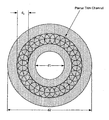
- the resistance value (R) is expressed by equation (1) in terms of the annular ring inner diameter (d 1 ) and outer diameter (d 2 ), resistive body thickness (T) and body resistivity (p).
- R ⁇ T K d 1 d 2 K ⁇ 2 ⁇ ⁇ T ⁇ In d 2 d 1 ⁇ ohms
- the factor K takes into account the reduction in resistance due to manufacturing (e.g., printing, lamination and thermal cycles).
- Equation (2) expresses the first order change in resistance tolerance for annular resistors with respect to the parameters of equation (1).
- ⁇ ⁇ R R ⁇ ⁇ d 2 d 2 - ⁇ ⁇ d 1 d 1 + In d 2 d 1 ⁇ ⁇ ⁇ ⁇ ⁇ - ⁇ ⁇ T T Equation (2) shows that a change in thickness or planning for annular resistors is multiplied by a natural log factor that is less than one for annular designs.
- the circuit substrate manufacturer can develop laser drill files that predictively trim annular resistors in a planar manner to provide controlled incremental changes in resistor thickness. In this manner, both small incremental and large resistance value changes can be achieved.
- the trim application can then use the predicted change in the resistance value associated with each laser drill file to assign the appropriate laser drill file to resistors within the appropriate resistance bin.
- the present invention is not limited to any specific passive component shape or methods of manufacturing such passive components.
- the laser trimming technique for annular resistors illustrated is an example of one component types.
- each laser drill file controls the laser drill to form a planar trim channel within the annular resistor.
- exemplary laser drill files may include parameters, such as laser beam spot size, pulse duration, aperture, energy, angle, step size, overlap factor and number of revolutions around the annular resistor, to cause the laser drill to perform a drill pattern on the annular resistor to form the planar trim channel.
- some embodiments may cause the laser drill to generate a pulse having a predefined aperture diameter (d a ) on a portion of the annular resistor, and then move the laser drill and generate another pulse on another portion of the annular resistor. This process may be repeated until the laser drill has carved a planar trim channel within the annular resistor.
- the width of the planar channel is equal to d 3 as illustrated in Figure 3 .
- the laser drill file may offset the laser drill by a predetermined amount and repeat the pattern in order to form a planar channel having more uniform side walls.
- Another embodiment may perform one or more revolutions at a relatively high power level in order to produce a relatively large change in resistance value, and then reduce the power level and perform one or more revolutions at a lower power setting in order to produce finer grained changes in resistance value.
- Still other embodiments may use a relatively large step size for one or more revolutions and a smaller step size on subsequent revolutions.
- other embodiments may use combinations of the foregoing processes or another configuration of control parameters to cause the laser drill to form a planar trim channel within the annular resistor.
- the drill format button 280 may be used to generate a formatted program that can be uploaded to a laser drill.
- This formatted program essentially incorporates the location (x, y coordinates) for each resistor into the laser drill file associated with that resistor, and then concatenates the laser drill files for all resistors into a single file. In this way, a single file can be created to perform laser trimming.
- laser trimming in accordance with embodiments of the present invention can avoid the difficult and often time consuming process of assigning laser trimming settings to each individual resistor on the circuit substrate layer.
- laser trimming processes can be easily adjusted by modifying laser trim files associated with individual bins based on measured performance in order to fine tune laser trimming processes.
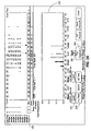
- FIG. 2B exemplary output of the trim tool assignment interface after performing laser trimming in accordance with an embodiment of the present invention is illustrated.
- the user can load post-laser trimming data by pressing the second load button 251 and entering the file name that stores the data.
- the post-laser trimming data can then be viewed by pressing the second test button 260.
- the resistance values for all images after laser trimming are much closer to target tolerances than the resistance values before laser trimming.
- all six images in this example have passed the applicable acceptance criteria after laser trimming as indicated by the pass parameter 240.
- the exemplary interface of Figure 2B also includes tools for monitoring and adjusting the performance of individual laser drill files.
- the user can view the distribution of resistance values for resistors trimmed using that particular laser drill file number in box 295. This information may be used to adjust the laser drill file by, for example, adjusting the power levels, step size, number of revolutions or other configuration parameters.
- Figure 5 illustrates exemplary yields for layered circuit boards achieved by processes performed in accordance with embodiments of the present invention.
- the table illustrated in Figure 5 shows the results after combining the results for the resistor core layers illustrated in Figures 4A and 4B .
- the individual yields for the two layers must be optimized to achieve the best overall yield.
- there was very little yield loss after lamination as shown by the 85% yield after final test for the individual images.
Landscapes
- Engineering & Computer Science (AREA)
- Microelectronics & Electronic Packaging (AREA)
- Physics & Mathematics (AREA)
- Optics & Photonics (AREA)
- Plasma & Fusion (AREA)
- Manufacturing & Machinery (AREA)
- Mechanical Engineering (AREA)
- Apparatuses And Processes For Manufacturing Resistors (AREA)
Claims (20)
- Procédé d'ajustage laser de résistances, le procédé comprenant :la mesure (158) d'une valeur de résistance pour chaque résistance d'un ensemble de résistances sur une couche de substrat de circuit ;le tri (160) des résistances en un ou plusieurs groupes (166) sur la base des valeurs de résistance mesurées et de valeurs de résistance cibles associées à chaque résistance ;l'affectation (162) d'un fichier d'ajustage laser (154) à chaque groupe sur la base d'une formulation d'ajustage prédictive, chaque fichier d'ajustage laser définissant un ensemble de paramètres de configuration (192) pour une perceuse laser (156) afin d'adapter chaque résistance à sa valeur cible respective ; etl'utilisation de la perceuse laser pour ajuster les résistances à l'intérieur de chaque groupe en fonction du fichier d'ajustage laser affecté à ce groupe ;dans lequel le fichier d'ajustage laser définit également un motif de perçage sur la résistance pour former un canal plan à l'intérieur de la résistance.
- Procédé selon la revendication 1, dans lequel les paramètres de configuration définis par le fichier d'ajustage laser comprennent au moins une taille de point et un niveau de puissance pour le perçage laser.
- Procédé selon la revendication 1, dans lequel les résistances comprennent des résistances annulaires.
- Procédé selon la revendication 3, dans lequel le fichier d'ajustage laser comprend au moins une taille de pas, un facteur de chevauchement et un nombre de pas d'avance sur la résistance pour former le canal plan.
- Procédé selon la revendication 1, comprenant en outre :la mesure d'une valeur de résistance de chaque résistance ajustée associée à un groupe particulier ; etl'ajustement du fichier d'ajustage laser associé au groupe particulier sur la base d'une distribution des valeurs de résistance mesurées des résistances ajustées à l'intérieur du groupe particulier.
- Procédé selon la revendication 1, comprenant en outre :la mesure d'une valeur de résistance de chaque résistance ajustée associée à un groupe particulier ; etl'affichage d'une distribution des valeurs de résistance ajustées pour évaluer les performances du fichier d'ajustage laser associé au groupe particulier.
- Procédé selon la revendication 1, comprenant en outre l'affichage d'une distribution des valeurs de résistance mesurées associées à chaque groupe pour évaluer les performances d'un procédé de formation d'un composant passif sous-jacent.
- Procédé selon la revendication 1, dans lequel la couche de substrat de circuit comprend une carte de circuit imprimé.
- Application d'ajustage (152) pour un système d'ajustage laser de résistances formées sur une couche de substrat de circuit, l'application d'ajustage étant configurée :pour recevoir une valeur de résistance mesurée par un testeur (150) pour chaque résistance d'un ensemble de résistances sur la couche de substrat de circuit ;pour trier (160) les résistances en un ou plusieurs groupes sur la base des valeurs de résistance mesurées et de valeurs de résistance cibles associées à chaque résistance ;pour affecter (162) un fichier d'ajustage laser (154) à chaque groupe sur la base d'une formulation d'ajustage prédictive afin d'adapter chaque résistance à sa valeur cible respective, chaque fichier d'ajustage laser définissant un ensemble de paramètres de configuration (192) pour une perceuse laser (156) configurée pour ajuster les résistances à l'intérieur de chaque groupe en fonction du fichier d'ajustage laser affecté à ce groupe, et définissant en outre un motif d'ajustage sur la résistance pour former un canal plan à l'intérieur de la résistance.
- Application d'ajustage selon la revendication 9, dans laquelle les paramètres de configuration définis par le fichier d'ajustage laser comprennent au moins une taille de point et un niveau de puissance pour la perceuse laser.
- Application d'ajustage selon la revendication 9, dans laquelle les résistances comprennent des résistances annulaires.
- Application d'ajustage selon la revendication 9, dans laquelle le fichier d'ajustage laser comprend au moins une taille de pas, un facteur de chevauchement et un nombre de pas d'avance sur la résistance pour former le canal plan.
- Application d'ajustage selon la revendication 9, en outre configurée :pour recevoir une valeur de résistance de chaque résistance annulaire ajustée associée à un groupe particulier ; etpour ajuster le fichier d'ajustage laser associé au groupe particulier sur la base d'une distribution des valeurs de résistance mesurées des résistances annulaires ajustées à l'intérieur du groupe particulier.
- Application d'ajustage selon la revendication 9, en outre configurée :pour recevoir une valeur de résistance de chaque résistance ajustée associée à un groupe particulier ; etpour afficher une distribution des valeurs de résistance ajustées afin d'évaluer les performances du fichier de perçage laser associé au groupe particulier.
- Application d'ajustage selon la revendication 9, également configurée :pour afficher une distribution des valeurs de résistance mesurées associées à chaque groupe afin d'évaluer les performances d'un procédé de formation d'un composant passif sous-jacent.
- Application d'ajustage selon la revendication 9, dans laquelle la couche de substrat de circuit comprend une carte de circuit imprimé.
- Système pour l'ajustage laser de résistances formées sur une couche de substrat de circuit, le système comprenant :un testeur (150) configuré pour mesurer une valeur de résistance pour chaque résistance d'un ensemble de résistances formées sur une couche de substrat de circuit ;l'application d'ajustage (152) de l'une quelconque des revendications 9 à 16 ; etune perceuse laser (156) configurée pour ajuster les résistances à l'intérieur de chaque groupe en fonction du fichier d'ajustage laser affecté à ce groupe.
- Système selon la revendication 17, dans lequel le testeur est configuré pour mesurer une valeur de résistance de chaque résistance annulaire ajustée associée à un groupe particulier.
- Système selon la revendication 17 ou la revendication 18, comprenant :une banque de fichiers d'ajustage laser (154), chaque fichier d'ajustage laser définissant un ensemble de paramètres de configuration (192) pour une perceuse laser afin d'adapter chaque résistance à sa valeur cible respective.
- Système selon la revendication 19, dans lequel les fichiers d'ajustage laser sont au format Excellon.
Applications Claiming Priority (5)
| Application Number | Priority Date | Filing Date | Title |
|---|---|---|---|
| US10/302,099 US6972391B2 (en) | 2002-11-21 | 2002-11-21 | Laser trimming of annular passive components |
| US302099 | 2002-11-21 | ||
| US454253 | 2003-06-03 | ||
| US10/454,253 US6940038B2 (en) | 2002-11-21 | 2003-06-03 | Laser trimming of resistors |
| PCT/US2003/037439 WO2004049401A2 (fr) | 2002-11-21 | 2003-11-20 | Ajustage au laser de resistances |
Publications (4)
| Publication Number | Publication Date |
|---|---|
| EP1567302A2 EP1567302A2 (fr) | 2005-08-31 |
| EP1567302A4 EP1567302A4 (fr) | 2009-07-29 |
| EP1567302B1 true EP1567302B1 (fr) | 2013-02-27 |
| EP1567302B8 EP1567302B8 (fr) | 2013-05-15 |
Family
ID=32396703
Family Applications (1)
| Application Number | Title | Priority Date | Filing Date |
|---|---|---|---|
| EP03783744.0A Expired - Lifetime EP1567302B8 (fr) | 2002-11-21 | 2003-11-20 | Ajustage au laser de resistances |
Country Status (5)
| Country | Link |
|---|---|
| US (1) | US7329831B2 (fr) |
| EP (1) | EP1567302B8 (fr) |
| JP (1) | JP5091406B2 (fr) |
| AU (1) | AU2003291150A1 (fr) |
| WO (1) | WO2004049401A2 (fr) |
Families Citing this family (8)
| Publication number | Priority date | Publication date | Assignee | Title |
|---|---|---|---|---|
| EP1567302B8 (fr) | 2002-11-21 | 2013-05-15 | Hadco Santa Clara, Inc. | Ajustage au laser de resistances |
| US7297896B2 (en) | 2002-11-21 | 2007-11-20 | Hadco Santa Clara, Inc. | Laser trimming of resistors |
| KR101225024B1 (ko) * | 2004-09-13 | 2013-01-23 | 일렉트로 싸이언티픽 인더스트리이즈 인코포레이티드 | 저항의 레이저 트리밍 동안 열전기적 전위 해소 |
| US20090199141A1 (en) * | 2008-02-06 | 2009-08-06 | Anritsu Company | Systems and methods for prototyping and testing electrical circuits in near real-time |
| US9060152B2 (en) | 2012-08-17 | 2015-06-16 | Flextronics Ap, Llc | Remote control having hotkeys with dynamically assigned functions |
| EP2903009A1 (fr) * | 2014-02-04 | 2015-08-05 | Telefonaktiebolaget L M Ericsson (publ) | Dispositif électronique, circuit et procédé permettant d'ajuster des composants électroniques |
| CN114019244A (zh) * | 2021-11-02 | 2022-02-08 | 洛阳银杏科技有限公司 | 一种激光调阻机测控系统及其方法 |
| EP4529369A1 (fr) * | 2023-09-21 | 2025-03-26 | AT & S Austria Technologie & Systemtechnik Aktiengesellschaft | Procédé de fabrication d'au moins une couche de structure conductrice sur ou dans un support de composant |
Family Cites Families (74)
| Publication number | Priority date | Publication date | Assignee | Title |
|---|---|---|---|---|
| US3388461A (en) * | 1965-01-26 | 1968-06-18 | Sperry Rand Corp | Precision electrical component adjustment method |
| US4301439A (en) | 1978-12-26 | 1981-11-17 | Electro Materials Corp. Of America | Film type resistor and method of producing same |
| US4566936A (en) * | 1984-11-05 | 1986-01-28 | North American Philips Corporation | Method of trimming precision resistors |
| US4795881A (en) * | 1987-06-02 | 1989-01-03 | Teradyne, Inc. | Curved electrical components and laser trimming thereof |
| US4998207A (en) * | 1988-02-01 | 1991-03-05 | Cooper Industries, Inc. | Method of manufacture of circuit boards |
| US4870746A (en) * | 1988-11-07 | 1989-10-03 | Litton Systems, Inc. | Method of making a multilayer printed circuit board having screened-on resistors |
| JPH03214602A (ja) * | 1990-01-18 | 1991-09-19 | Matsushita Electric Ind Co Ltd | 電子回路部品の製造方法 |
| JP2523934B2 (ja) * | 1990-04-26 | 1996-08-14 | 松下電器産業株式会社 | サ―マルヘッドの抵抗値トリミング法 |
| JP2818489B2 (ja) * | 1990-12-29 | 1998-10-30 | 京セラ株式会社 | 薄膜サーマルヘッドの抵抗体トリミング方法 |
| US5404143A (en) | 1991-06-12 | 1995-04-04 | Intellectual Property Development Associates Of Connecticut, Inc. | Network swappers and circuits constructed from same |
| JPH05135911A (ja) * | 1991-07-02 | 1993-06-01 | Tateyama Kagaku Kogyo Kk | サーミスタのトリミング方法 |
| US5481129A (en) | 1991-10-30 | 1996-01-02 | Harris Corporation | Analog-to-digital converter |
| US5856695A (en) | 1991-10-30 | 1999-01-05 | Harris Corporation | BiCMOS devices |
| US5994755A (en) | 1991-10-30 | 1999-11-30 | Intersil Corporation | Analog-to-digital converter and method of fabrication |
| TW222364B (fr) * | 1992-05-28 | 1994-04-11 | Digital Equipment Corp | |
| US5443534A (en) | 1992-07-21 | 1995-08-22 | Vlt Corporation | Providing electronic components for circuity assembly |
| US5420515A (en) | 1992-08-28 | 1995-05-30 | Hewlett-Packard Company | Active circuit trimming with AC and DC response trims relative to a known response |
| US5265114C1 (en) | 1992-09-10 | 2001-08-21 | Electro Scient Ind Inc | System and method for selectively laser processing a target structure of one or more materials of a multimaterial multilayer device |
| US5502468A (en) | 1992-12-28 | 1996-03-26 | Tektronix, Inc. | Ink jet print head drive with normalization |
| US5603847A (en) | 1993-04-07 | 1997-02-18 | Zycon Corporation | Annular circuit components coupled with printed circuit board through-hole |
| US5347258A (en) | 1993-04-07 | 1994-09-13 | Zycon Corporation | Annular resistor coupled with printed circuit board through-hole |
| US5504470A (en) | 1993-10-12 | 1996-04-02 | Cts Corporation | Resistor trimming process for high voltage surge survival |
| US5504681A (en) | 1994-06-29 | 1996-04-02 | Ford Motor Company | Mass air flow sensor calibration |
| CA2150502A1 (fr) | 1994-08-05 | 1996-02-06 | Michael F. Mattes | Methode et appareil servant a mesurer la temperature |
| JP3114006B2 (ja) | 1994-08-29 | 2000-12-04 | セイコーインスツルメンツ株式会社 | 半導体装置、及び、その製造方法 |
| US5540092A (en) | 1994-10-31 | 1996-07-30 | Handfield; Michael | System and method for monitoring a pneumatic tire |
| US5504986A (en) | 1995-03-02 | 1996-04-09 | Hewlett-Packard Company | Method of manufacturing collinear terminated transmission line structure with thick film circuitry |
| JP3552791B2 (ja) | 1995-06-13 | 2004-08-11 | 松下電器産業株式会社 | 電子部品実装方法及び装置 |
| US5900530A (en) | 1995-07-31 | 1999-05-04 | Motorola, Inc. | Method for testing pressure sensors |
| US5701097A (en) | 1995-08-15 | 1997-12-23 | Harris Corporation | Statistically based current generator circuit |
| US5600071A (en) | 1995-09-05 | 1997-02-04 | Motorola, Inc. | Vertically integrated sensor structure and method |
| US5779918A (en) | 1996-02-14 | 1998-07-14 | Denso Corporation | Method for manufacturing a photo-sensor |
| JPH09270308A (ja) * | 1996-03-29 | 1997-10-14 | Chichibu Onoda Cement Corp | 面状厚膜抵抗体及びその抵抗値調整方法 |
| US5946210A (en) | 1996-04-19 | 1999-08-31 | Vlt Corporation | Configuring power converters |
| US5881451A (en) | 1996-06-21 | 1999-03-16 | Xerox Corporation | Sensing the temperature of a printhead in an ink jet printer |
| JPH1032110A (ja) * | 1996-07-16 | 1998-02-03 | Matsushita Refrig Co Ltd | 厚膜抵抗体のレーザトリミング方法 |
| US5850171A (en) | 1996-08-05 | 1998-12-15 | Cyntec Company | Process for manufacturing resistor-networks with higher circuit density, smaller input/output pitches, and lower precision tolerance |
| US5771012A (en) | 1996-09-11 | 1998-06-23 | Harris Corporation | Integrated circuit analog-to-digital converter and associated calibration method and apparatus |
| US5958606A (en) | 1997-02-05 | 1999-09-28 | Cyntec Company | Substrate structure with adhesive anchoring-seams for securely attaching and boding to a thin film supported thereon |
| US5753571A (en) | 1997-02-13 | 1998-05-19 | E. I. Du Pont De Nemours And Company | Lead and cadmium-free encapsulant composition |
| AT406025B (de) * | 1997-07-22 | 2000-01-25 | M & R Automatisierung Von Indu | Mess- und sortieranlagen zum messen und sortieren von widerstandskörper sowie ein verfahren |
| US5874887A (en) | 1997-08-27 | 1999-02-23 | Kosinski; John P. | Trimmed surge resistors |
| US6107909A (en) | 1997-08-27 | 2000-08-22 | Microlectronic Modules Corporation | Trimmed surge resistors |
| US5969658A (en) | 1997-11-18 | 1999-10-19 | Burr-Brown Corporation | R/2R ladder circuit and method for digital-to-analog converter |
| US5994997A (en) | 1997-11-24 | 1999-11-30 | Motorola, Inc. | Thick-film resistor having concentric terminals and method therefor |
| US5926123A (en) | 1997-12-08 | 1999-07-20 | Raytheon Company | Self calibration circuitry and algorithm for multipass analog to digital converter interstage gain correction |
| US6100815A (en) | 1997-12-24 | 2000-08-08 | Electro Scientific Industries, Inc. | Compound switching matrix for probing and interconnecting devices under test to measurement equipment |
| US6072943A (en) | 1997-12-30 | 2000-06-06 | Lsi Logic Corporation | Integrated bus controller and terminating chip |
| US6084424A (en) | 1997-12-30 | 2000-07-04 | Lsi Logic Corporation | Adjustable biasing voltage for a bus line and associated method |
| US5977797A (en) | 1997-12-30 | 1999-11-02 | Lsi Logic Corporation | Method and apparatus for transferring data on a voltage biased data line |
| US5973631A (en) | 1998-01-20 | 1999-10-26 | Raytheon Company | Test circuit and method of trimming a unary digital-to-analog converter (DAC) in a subranging analog-to-digital converter (ADC) |
| US5939693A (en) | 1998-02-02 | 1999-08-17 | Motorola Inc. | Polynomial calculator device, and method therefor |
| US5995033A (en) | 1998-02-02 | 1999-11-30 | Motorola Inc. | Signal conditioning circuit including a combined ADC/DAC, sensor system, and method therefor |
| US6041007A (en) | 1998-02-02 | 2000-03-21 | Motorola, Inc. | Device with programmable memory and method of programming |
| US6269151B1 (en) * | 1998-03-13 | 2001-07-31 | At&T Corp. | System and method for delivering voice messages to voice mail systems |
| US6225035B1 (en) | 1998-03-18 | 2001-05-01 | Motorola, Inc. | Method for forming a thick-film resistor |
| FR2780601B1 (fr) | 1998-06-24 | 2000-07-21 | Commissariat Energie Atomique | Procede de depot par plasma a la resonance cyclotron electronique de couches de carbone emetteur d'electrons sous l'effet d'un champ electrique applique |
| US6150681A (en) | 1998-07-24 | 2000-11-21 | Silicon Microstructures, Inc. | Monolithic flow sensor and pressure sensor |
| US5977863A (en) | 1998-08-10 | 1999-11-02 | Cts Corporation | Low cross talk ball grid array resistor network |
| US6120835A (en) | 1998-10-05 | 2000-09-19 | Honeywell International Inc. | Process for manufacture of thick film hydrogen sensors |
| JP3943264B2 (ja) * | 1998-10-20 | 2007-07-11 | ローム株式会社 | サーマルプリントヘッドのトリミング方法 |
| US6020785A (en) | 1998-10-23 | 2000-02-01 | Maxim Integrated Products, Inc. | Fixed gain operational amplifiers |
| US6180164B1 (en) | 1998-10-26 | 2001-01-30 | Delco Electronics Corporation | Method of forming ruthenium-based thick-film resistors |
| US6225576B1 (en) | 1999-04-20 | 2001-05-01 | Cts Corporation | Shear beam load cell |
| US6187372B1 (en) | 1999-04-29 | 2001-02-13 | Agilent Technologies, Inc. | Method for producing large area thick film resistors with uniform thickness |
| US6268225B1 (en) | 1999-07-15 | 2001-07-31 | Viking Technology Corporation | Fabrication method for integrated passive component |
| US6259151B1 (en) | 1999-07-21 | 2001-07-10 | Intersil Corporation | Use of barrier refractive or anti-reflective layer to improve laser trim characteristics of thin film resistors |
| US6140872A (en) | 1999-10-28 | 2000-10-31 | Burr-Brown Corporation | Offset-compensated amplifier input stage and method |
| US6246312B1 (en) | 2000-07-20 | 2001-06-12 | Cts Corporation | Ball grid array resistor terminator network |
| JP2002043195A (ja) * | 2000-07-27 | 2002-02-08 | Hitachi Metals Ltd | 電子部品の特性調整方法 |
| JP2002144056A (ja) * | 2000-11-06 | 2002-05-21 | Ibiden Co Ltd | レーザトリミングステージ |
| US6875950B2 (en) * | 2002-03-22 | 2005-04-05 | Gsi Lumonics Corporation | Automated laser trimming of resistors |
| CN1705639A (zh) | 2002-09-20 | 2005-12-07 | 惠氏控股公司 | 用于合成微管蛋白抑制剂的中间体的合成方法 |
| EP1567302B8 (fr) | 2002-11-21 | 2013-05-15 | Hadco Santa Clara, Inc. | Ajustage au laser de resistances |
-
2003
- 2003-11-20 EP EP03783744.0A patent/EP1567302B8/fr not_active Expired - Lifetime
- 2003-11-20 JP JP2005510391A patent/JP5091406B2/ja not_active Expired - Lifetime
- 2003-11-20 WO PCT/US2003/037439 patent/WO2004049401A2/fr not_active Ceased
- 2003-11-20 AU AU2003291150A patent/AU2003291150A1/en not_active Abandoned
-
2005
- 2005-03-29 US US11/094,003 patent/US7329831B2/en not_active Expired - Lifetime
Also Published As
| Publication number | Publication date |
|---|---|
| EP1567302A4 (fr) | 2009-07-29 |
| JP5091406B2 (ja) | 2012-12-05 |
| EP1567302B8 (fr) | 2013-05-15 |
| WO2004049401A2 (fr) | 2004-06-10 |
| EP1567302A2 (fr) | 2005-08-31 |
| WO2004049401A3 (fr) | 2005-02-17 |
| AU2003291150A1 (en) | 2004-06-18 |
| JP2006508551A (ja) | 2006-03-09 |
| US20050168318A1 (en) | 2005-08-04 |
| US7329831B2 (en) | 2008-02-12 |
| AU2003291150A8 (en) | 2004-06-18 |
Similar Documents
| Publication | Publication Date | Title |
|---|---|---|
| JP5095796B2 (ja) | レジスタのレーザトリミング | |
| EP1567302B1 (fr) | Ajustage au laser de resistances | |
| US6875950B2 (en) | Automated laser trimming of resistors | |
| EP3530463B1 (fr) | Appareil et procédé de génération d'un paramètre de commande d'une machine de sérigraphie | |
| US4649497A (en) | Computer-produced circuit board | |
| CN104427774B (zh) | 基于测量pcb特定子区中锡膏沉积物改变印刷控制参数 | |
| CN104317998B (zh) | 一种Gerber文件的参数的制造补偿的方法和装置 | |
| JP2003249763A (ja) | 多層配線基板及びその製造方法 | |
| US7297896B2 (en) | Laser trimming of resistors | |
| KR101475530B1 (ko) | 비아 천공의 품질 관리 및 분석을 위한 프로세스 및 시스템 | |
| US8763240B2 (en) | Fabrication process for embedded passive components | |
| KR101604315B1 (ko) | 다층 회로 기판의 캠 작업에 대한 자동화 방법 | |
| CN117015150B (zh) | 一种电路板智能生产工艺、控制系统、装置及存储介质 | |
| CN103517556A (zh) | 一种电路板控深钻孔深度确定方法及电路板 | |
| CN108684150B (zh) | 印制电路板钻孔的孔限计算方法及系统 | |
| US6917848B1 (en) | Production system for printed wiring board | |
| JP4223412B2 (ja) | メッキリード評価プログラム、このメッキリード評価プログラムを記録したコンピュータ読み取り可能な記録媒体を備えた評価装置、およびこれらメッキリード評価プログラムまたは評価装置を用いて設計されたプリント配線板 | |
| JP2021023982A (ja) | 半田付け条件学習装置、半田付け条件決定装置及び半田付け装置 | |
| JP4071351B2 (ja) | プリント基板設計cadシステム | |
| WO2025209687A1 (fr) | Ensemble de mesure de courant, système d'équilibrage, procédé d'équilibrage et procédé de production d'un ensemble de mesure de courant | |
| US20070236895A1 (en) | Via resistor structure and method for trimming resistance value | |
| Jones et al. | Embedded passive technology for networking systems | |
| JP2760517B2 (ja) | 半導体集積回路補修支援方法および装置 | |
| JP2021117623A (ja) | クロストークチェック装置 | |
| CN107038304A (zh) | 一种快速生成pcb制作单的方法 |
Legal Events
| Date | Code | Title | Description |
|---|---|---|---|
| PUAI | Public reference made under article 153(3) epc to a published international application that has entered the european phase |
Free format text: ORIGINAL CODE: 0009012 |
|
| 17P | Request for examination filed |
Effective date: 20050521 |
|
| AK | Designated contracting states |
Kind code of ref document: A2 Designated state(s): AT BE BG CH CY CZ DE DK EE ES FI FR GB GR HU IE IT LI LU MC NL PT RO SE SI SK TR |
|
| AX | Request for extension of the european patent |
Extension state: AL LT LV MK |
|
| DAX | Request for extension of the european patent (deleted) | ||
| A4 | Supplementary search report drawn up and despatched |
Effective date: 20090629 |
|
| RIC1 | Information provided on ipc code assigned before grant |
Ipc: B23K 26/38 20060101AFI20050601BHEP Ipc: H01C 17/242 20060101ALI20090623BHEP |
|
| 17Q | First examination report despatched |
Effective date: 20091030 |
|
| REG | Reference to a national code |
Ref country code: DE Ref legal event code: R079 Ref document number: 60343397 Country of ref document: DE Free format text: PREVIOUS MAIN CLASS: B23K0026380000 Ipc: H05K0001160000 |
|
| RIC1 | Information provided on ipc code assigned before grant |
Ipc: B23K 26/00 20060101ALI20110907BHEP Ipc: H01C 17/242 20060101ALI20110907BHEP Ipc: H05K 1/16 20060101AFI20110907BHEP Ipc: H05K 13/08 20060101ALI20110907BHEP |
|
| GRAP | Despatch of communication of intention to grant a patent |
Free format text: ORIGINAL CODE: EPIDOSNIGR1 |
|
| GRAS | Grant fee paid |
Free format text: ORIGINAL CODE: EPIDOSNIGR3 |
|
| GRAA | (expected) grant |
Free format text: ORIGINAL CODE: 0009210 |
|
| RAP1 | Party data changed (applicant data changed or rights of an application transferred) |
Owner name: HADCO SANTA CLARA, INC. |
|
| AK | Designated contracting states |
Kind code of ref document: B1 Designated state(s): AT BE BG CH CY CZ DE DK EE ES FI FR GB GR HU IE IT LI LU MC NL PT RO SE SI SK TR |
|
| REG | Reference to a national code |
Ref country code: GB Ref legal event code: FG4D |
|
| REG | Reference to a national code |
Ref country code: CH Ref legal event code: EP |
|
| REG | Reference to a national code |
Ref country code: AT Ref legal event code: REF Ref document number: 599068 Country of ref document: AT Kind code of ref document: T Effective date: 20130315 |
|
| REG | Reference to a national code |
Ref country code: IE Ref legal event code: FG4D |
|
| REG | Reference to a national code |
Ref country code: DE Ref legal event code: R096 Ref document number: 60343397 Country of ref document: DE Effective date: 20130425 |
|
| RAP2 | Party data changed (patent owner data changed or rights of a patent transferred) |
Owner name: HADCO SANTA CLARA, INC. |
|
| REG | Reference to a national code |
Ref country code: DE Ref legal event code: R082 Ref document number: 60343397 Country of ref document: DE Representative=s name: D YOUNG & CO LLP, GB |
|
| REG | Reference to a national code |
Ref country code: SE Ref legal event code: TRGR |
|
| REG | Reference to a national code |
Ref country code: NL Ref legal event code: T3 |
|
| PG25 | Lapsed in a contracting state [announced via postgrant information from national office to epo] |
Ref country code: ES Free format text: LAPSE BECAUSE OF FAILURE TO SUBMIT A TRANSLATION OF THE DESCRIPTION OR TO PAY THE FEE WITHIN THE PRESCRIBED TIME-LIMIT Effective date: 20130607 Ref country code: BG Free format text: LAPSE BECAUSE OF FAILURE TO SUBMIT A TRANSLATION OF THE DESCRIPTION OR TO PAY THE FEE WITHIN THE PRESCRIBED TIME-LIMIT Effective date: 20130527 |
|
| PG25 | Lapsed in a contracting state [announced via postgrant information from national office to epo] |
Ref country code: FI Free format text: LAPSE BECAUSE OF FAILURE TO SUBMIT A TRANSLATION OF THE DESCRIPTION OR TO PAY THE FEE WITHIN THE PRESCRIBED TIME-LIMIT Effective date: 20130227 Ref country code: GR Free format text: LAPSE BECAUSE OF FAILURE TO SUBMIT A TRANSLATION OF THE DESCRIPTION OR TO PAY THE FEE WITHIN THE PRESCRIBED TIME-LIMIT Effective date: 20130528 Ref country code: SI Free format text: LAPSE BECAUSE OF FAILURE TO SUBMIT A TRANSLATION OF THE DESCRIPTION OR TO PAY THE FEE WITHIN THE PRESCRIBED TIME-LIMIT Effective date: 20130227 Ref country code: PT Free format text: LAPSE BECAUSE OF FAILURE TO SUBMIT A TRANSLATION OF THE DESCRIPTION OR TO PAY THE FEE WITHIN THE PRESCRIBED TIME-LIMIT Effective date: 20130627 Ref country code: BE Free format text: LAPSE BECAUSE OF FAILURE TO SUBMIT A TRANSLATION OF THE DESCRIPTION OR TO PAY THE FEE WITHIN THE PRESCRIBED TIME-LIMIT Effective date: 20130227 |
|
| PG25 | Lapsed in a contracting state [announced via postgrant information from national office to epo] |
Ref country code: CZ Free format text: LAPSE BECAUSE OF FAILURE TO SUBMIT A TRANSLATION OF THE DESCRIPTION OR TO PAY THE FEE WITHIN THE PRESCRIBED TIME-LIMIT Effective date: 20130227 Ref country code: SK Free format text: LAPSE BECAUSE OF FAILURE TO SUBMIT A TRANSLATION OF THE DESCRIPTION OR TO PAY THE FEE WITHIN THE PRESCRIBED TIME-LIMIT Effective date: 20130227 Ref country code: EE Free format text: LAPSE BECAUSE OF FAILURE TO SUBMIT A TRANSLATION OF THE DESCRIPTION OR TO PAY THE FEE WITHIN THE PRESCRIBED TIME-LIMIT Effective date: 20130227 Ref country code: RO Free format text: LAPSE BECAUSE OF FAILURE TO SUBMIT A TRANSLATION OF THE DESCRIPTION OR TO PAY THE FEE WITHIN THE PRESCRIBED TIME-LIMIT Effective date: 20130227 Ref country code: DK Free format text: LAPSE BECAUSE OF FAILURE TO SUBMIT A TRANSLATION OF THE DESCRIPTION OR TO PAY THE FEE WITHIN THE PRESCRIBED TIME-LIMIT Effective date: 20130227 |
|
| PG25 | Lapsed in a contracting state [announced via postgrant information from national office to epo] |
Ref country code: CY Free format text: LAPSE BECAUSE OF FAILURE TO SUBMIT A TRANSLATION OF THE DESCRIPTION OR TO PAY THE FEE WITHIN THE PRESCRIBED TIME-LIMIT Effective date: 20130227 |
|
| PLBE | No opposition filed within time limit |
Free format text: ORIGINAL CODE: 0009261 |
|
| STAA | Information on the status of an ep patent application or granted ep patent |
Free format text: STATUS: NO OPPOSITION FILED WITHIN TIME LIMIT |
|
| 26N | No opposition filed |
Effective date: 20131128 |
|
| REG | Reference to a national code |
Ref country code: DE Ref legal event code: R097 Ref document number: 60343397 Country of ref document: DE Effective date: 20131128 |
|
| PG25 | Lapsed in a contracting state [announced via postgrant information from national office to epo] |
Ref country code: MC Free format text: LAPSE BECAUSE OF FAILURE TO SUBMIT A TRANSLATION OF THE DESCRIPTION OR TO PAY THE FEE WITHIN THE PRESCRIBED TIME-LIMIT Effective date: 20130227 |
|
| REG | Reference to a national code |
Ref country code: IE Ref legal event code: MM4A |
|
| PG25 | Lapsed in a contracting state [announced via postgrant information from national office to epo] |
Ref country code: IE Free format text: LAPSE BECAUSE OF NON-PAYMENT OF DUE FEES Effective date: 20131120 |
|
| PG25 | Lapsed in a contracting state [announced via postgrant information from national office to epo] |
Ref country code: TR Free format text: LAPSE BECAUSE OF FAILURE TO SUBMIT A TRANSLATION OF THE DESCRIPTION OR TO PAY THE FEE WITHIN THE PRESCRIBED TIME-LIMIT Effective date: 20130227 |
|
| PG25 | Lapsed in a contracting state [announced via postgrant information from national office to epo] |
Ref country code: LU Free format text: LAPSE BECAUSE OF NON-PAYMENT OF DUE FEES Effective date: 20131120 Ref country code: HU Free format text: LAPSE BECAUSE OF FAILURE TO SUBMIT A TRANSLATION OF THE DESCRIPTION OR TO PAY THE FEE WITHIN THE PRESCRIBED TIME-LIMIT; INVALID AB INITIO Effective date: 20031120 |
|
| REG | Reference to a national code |
Ref country code: FR Ref legal event code: PLFP Year of fee payment: 13 |
|
| REG | Reference to a national code |
Ref country code: FR Ref legal event code: PLFP Year of fee payment: 14 |
|
| REG | Reference to a national code |
Ref country code: FR Ref legal event code: PLFP Year of fee payment: 15 |
|
| REG | Reference to a national code |
Ref country code: FR Ref legal event code: PLFP Year of fee payment: 16 |
|
| PGFP | Annual fee paid to national office [announced via postgrant information from national office to epo] |
Ref country code: NL Payment date: 20181114 Year of fee payment: 16 |
|
| PGFP | Annual fee paid to national office [announced via postgrant information from national office to epo] |
Ref country code: SE Payment date: 20181113 Year of fee payment: 16 Ref country code: AT Payment date: 20181025 Year of fee payment: 16 Ref country code: DE Payment date: 20181106 Year of fee payment: 16 |
|
| PGFP | Annual fee paid to national office [announced via postgrant information from national office to epo] |
Ref country code: CH Payment date: 20181115 Year of fee payment: 16 Ref country code: FR Payment date: 20181011 Year of fee payment: 16 Ref country code: GB Payment date: 20181114 Year of fee payment: 16 Ref country code: IT Payment date: 20181122 Year of fee payment: 16 |
|
| REG | Reference to a national code |
Ref country code: DE Ref legal event code: R119 Ref document number: 60343397 Country of ref document: DE |
|
| REG | Reference to a national code |
Ref country code: SE Ref legal event code: EUG Ref country code: CH Ref legal event code: PL |
|
| REG | Reference to a national code |
Ref country code: NL Ref legal event code: MM Effective date: 20191201 |
|
| PG25 | Lapsed in a contracting state [announced via postgrant information from national office to epo] |
Ref country code: LI Free format text: LAPSE BECAUSE OF NON-PAYMENT OF DUE FEES Effective date: 20191130 Ref country code: CH Free format text: LAPSE BECAUSE OF NON-PAYMENT OF DUE FEES Effective date: 20191130 |
|
| REG | Reference to a national code |
Ref country code: AT Ref legal event code: MM01 Ref document number: 599068 Country of ref document: AT Kind code of ref document: T Effective date: 20191120 |
|
| PG25 | Lapsed in a contracting state [announced via postgrant information from national office to epo] |
Ref country code: SE Free format text: LAPSE BECAUSE OF NON-PAYMENT OF DUE FEES Effective date: 20191121 |
|
| GBPC | Gb: european patent ceased through non-payment of renewal fee |
Effective date: 20191120 |
|
| PG25 | Lapsed in a contracting state [announced via postgrant information from national office to epo] |
Ref country code: NL Free format text: LAPSE BECAUSE OF NON-PAYMENT OF DUE FEES Effective date: 20191201 |
|
| PG25 | Lapsed in a contracting state [announced via postgrant information from national office to epo] |
Ref country code: FR Free format text: LAPSE BECAUSE OF NON-PAYMENT OF DUE FEES Effective date: 20191130 Ref country code: IT Free format text: LAPSE BECAUSE OF NON-PAYMENT OF DUE FEES Effective date: 20191120 Ref country code: DE Free format text: LAPSE BECAUSE OF NON-PAYMENT OF DUE FEES Effective date: 20200603 Ref country code: GB Free format text: LAPSE BECAUSE OF NON-PAYMENT OF DUE FEES Effective date: 20191120 |
|
| PG25 | Lapsed in a contracting state [announced via postgrant information from national office to epo] |
Ref country code: AT Free format text: LAPSE BECAUSE OF NON-PAYMENT OF DUE FEES Effective date: 20191120 |