EP1566831A2 - Dispositif a semi-conducteurs et procédé de fabrication dudit dispositif - Google Patents
Dispositif a semi-conducteurs et procédé de fabrication dudit dispositif Download PDFInfo
- Publication number
- EP1566831A2 EP1566831A2 EP05250899A EP05250899A EP1566831A2 EP 1566831 A2 EP1566831 A2 EP 1566831A2 EP 05250899 A EP05250899 A EP 05250899A EP 05250899 A EP05250899 A EP 05250899A EP 1566831 A2 EP1566831 A2 EP 1566831A2
- Authority
- EP
- European Patent Office
- Prior art keywords
- film
- resistance element
- metal thin
- produced
- metal
- Prior art date
- Legal status (The legal status is an assumption and is not a legal conclusion. Google has not performed a legal analysis and makes no representation as to the accuracy of the status listed.)
- Withdrawn
Links
Images


Classifications
-
- H—ELECTRICITY
- H10—SEMICONDUCTOR DEVICES; ELECTRIC SOLID-STATE DEVICES NOT OTHERWISE PROVIDED FOR
- H10D—INORGANIC ELECTRIC SEMICONDUCTOR DEVICES
- H10D84/00—Integrated devices formed in or on semiconductor substrates that comprise only semiconducting layers, e.g. on Si wafers or on GaAs-on-Si wafers
- H10D84/201—Integrated devices formed in or on semiconductor substrates that comprise only semiconducting layers, e.g. on Si wafers or on GaAs-on-Si wafers characterised by the integration of only components covered by H10D1/00 or H10D8/00, e.g. RLC circuits
- H10D84/204—Integrated devices formed in or on semiconductor substrates that comprise only semiconducting layers, e.g. on Si wafers or on GaAs-on-Si wafers characterised by the integration of only components covered by H10D1/00 or H10D8/00, e.g. RLC circuits of combinations of diodes or capacitors or resistors
- H10D84/209—Integrated devices formed in or on semiconductor substrates that comprise only semiconducting layers, e.g. on Si wafers or on GaAs-on-Si wafers characterised by the integration of only components covered by H10D1/00 or H10D8/00, e.g. RLC circuits of combinations of diodes or capacitors or resistors of only resistors
-
- H—ELECTRICITY
- H10—SEMICONDUCTOR DEVICES; ELECTRIC SOLID-STATE DEVICES NOT OTHERWISE PROVIDED FOR
- H10D—INORGANIC ELECTRIC SEMICONDUCTOR DEVICES
- H10D1/00—Resistors, capacitors or inductors
- H10D1/40—Resistors
- H10D1/47—Resistors having no potential barriers
- H10D1/474—Resistors having no potential barriers comprising refractory metals, transition metals, noble metals, metal compounds or metal alloys, e.g. silicides
-
- H—ELECTRICITY
- H10—SEMICONDUCTOR DEVICES; ELECTRIC SOLID-STATE DEVICES NOT OTHERWISE PROVIDED FOR
- H10D—INORGANIC ELECTRIC SEMICONDUCTOR DEVICES
- H10D86/00—Integrated devices formed in or on insulating or conducting substrates, e.g. formed in silicon-on-insulator [SOI] substrates or on stainless steel or glass substrates
- H10D86/80—Integrated devices formed in or on insulating or conducting substrates, e.g. formed in silicon-on-insulator [SOI] substrates or on stainless steel or glass substrates characterised by multiple passive components, e.g. resistors, capacitors or inductors
- H10D86/85—Integrated devices formed in or on insulating or conducting substrates, e.g. formed in silicon-on-insulator [SOI] substrates or on stainless steel or glass substrates characterised by multiple passive components, e.g. resistors, capacitors or inductors characterised by only passive components
-
- H10W20/498—
Definitions
- the present invention relates to a semiconductor device and a method for manufacturing it, and, in particular, to a semiconductor device having a metal thin-film resistance element made of a metal thin film produced on an insulating film and a manufacturing method therefor.
- a resistance element is heavily used as an essential element.
- a resistance element made of a metal thin film attracts an attention in terms of low temperature dependence of its resistance value (referred to as a TCR, hereinafter).
- a material of the metal thin-film resistance element for example, chrome silicon (CrSi), nickel chrome (NiCr), titanium nitride (TaN), chrome silicide (CrSi 2 ), chrome silicide nitride (CrSiN), chrome silicon oxy (CrSiO), or such is applied.
- the metal thin-film resistance element having a thin film thinness less than 1000 ⁇ is produced for achieving a higher sheet resistance, in many cases.
- the high-malting-point metal film 97 is partially removed selectively with the use of the metal wiring pattern 103 as a mask by means of wet etching technology, and thus, high-melting-point metal film patterns 105 are produced. Thereby, production of the metal thin-film resistance element 77 and the metal wiring patterns 103 for making electrical connections from the metal thin-film resistance element 77 is completed (see FIG. 27, (e)). There, since the high-melting-point metal film 97 exists immediately above the metal thin-film resistance element 77, patterning of the high-melting-point metal film 97 by means of dry etching technology is difficult (see FIG. 27, (d)).
- a semiconductor integrated circuit device having, not the metal thin-film resistance element, but a resistance element produced on a top layer wiring electrode via an insulating film, and connected with the top layer wiring electrode.
- a manufacturing method for a case where such a structure is applied to the metal thin-film resistance element is described next with reference to FIG. 28.
- the metal thin film 115 is patterned for a predetermined shape, and thus, the metal thin-film resistance element is produced therefrom.
- an integrated circuit having the metal thin-film resistor mounted on an insulating film of a semiconductor integrated circuit is disclosed (for example, see the patent document 7 listed below) in which contact at an electrode part of the metal thin-film resistor between the metal thin-film resistor and a metal wiring is made at least at a part on an end surface and a top surface of the metal wiring.
- the metal wiring pattern 83 is directly produced on the metal thin-film resistance element 77.
- the process (5) described with reference to FIG. 25, (e) it is not possible to apply dry etching for carrying out pattering of the wiring metal film 79.
- the metal thin-film resistance element 77 is easily oxidized in general, and, when the wiring metal film 79 is provided on the metal thin-film resistance element 77 after a surface thereof is oxidized, a satisfactory electrical connection between the metal thin-film resistance element 77 and the wiring metal film 79 may not be achieved. In a common semiconductor manufacturing process, a satisfactory electrical connection with a metal wiring may be achieved as a result of a natural oxide film on a surface of a silicon substrate being removed by means of hydrofluoric acid solution.
- a resistance value of the metal thin-film resistance element 77 may vary if the oxide film removing processing with hydrofluoric acid is carried out before the wiring metal film 79 is produced in the above-mentioned process (4) described above with reference to FIG. 25, (d).
- wet etching processing is required in some process by the reason that the film thickness of the metal thin-film resistance element is very small. As a result, fine working may be obstructed, or, variation in the resistance value may occur.
- the metal thin-film resistance element is easily oxidized, and if so, it is difficult to achieve a satisfactory electrical connection with the metal wiring, it is necessary to add a special process to produce a barrier film to protect the metal thin-film resistance element, or to carry out surface oxide film removing processing with the use of hydrofluoric acid, or such.
- the number of manufacturing processes increases or the resistance value may vary, accordingly.
- step coverage of the metal thin film 115 may degrade on an inner side surfaces of the connecting holes 113, in particular, on the side of the bottom of each connecting hole 113.
- the contact resistance between the metal thin-film resistance element and the wiring pattern 107 may increase and vary.
- diameters of the connecting holes or the step coverage of the metal thin film may vary, and further, the contact resistance may vary.
- the second interlayer insulating film 109 is etched, and also, a part of the wiring pattern 107 on the top side is etched due to over-etching.
- a product made of Al, C, F or such is produced when the wiring pattern 107 is etched during over-etching.
- Such a product may not be able to be completely removed in a post processing, and unevenness occurring due to the product may cause variation of the contact resistance between the metal thin-fill resistance element and the wiring patterns 107.
- the processes of pattering the resist with the use of photoengraving etching, production of the connecting holes with the use of dry etching technology, removal of the resist, removal of an etching reaction product from the inside of the connecting holes and so forth are required, and thus, the manufacturing method may become complicated.
- the electrode part of the metal thin-film resistance element is produced to cover the end surface and the top surface of the end part of the metal wiring.
- the step coverage of the metal thin-film resistance element may degrade.
- the resistance value may increase, or breakage of the metal thin-film resistance element may occur.
- An aim of the present invention is to achieve stabilization of a resistance value of the metal thin-film resistance element including a contact resistance with an electrode produced from a part of a wiring pattern in a semiconductor device having the metal thin-film resistance element and a method of manufacturing it.
- a semiconductor device includes: an insulating film; a metal thin-film resistance element; a wiring pattern formed on the insulating film, a part of which forms an electrode for electrically connecting with the metal thin-film resistance element; and a side wall produced at least on a side surface of the electrode of the wiring pattern, and made of an insulation material, wherein: the metal thin-film resistance element is produced over from a top surface of the electrode through a surface of the insulating film across a surface of the side wall.
- a second side wall including Ar may be produced on a surface of the side wall on the side of the insulating film.
- the second side wall including Ar may be produced by carrying out Ar sputter etching processing (which may also be called inverse sputtering processing) after producing the wiring pattern and the side wall.
- a semiconductor device includes: a first insulating film; a metal thin-film resistance element; a wiring pattern formed on the first insulating film; and a second insulating film on the first insulating film with a film thickness such that a top surface of the wiring pattern may be exposed, wherein: the metal thin-film resistance element is produced over from a top surface of the electrode through a surface of the second insulating film.
- a part of the metal thin-film resistance element may intersect the wiring pattern on the electrode.
- the above-mentioned 'a part of the metal thin-film resistance element may intersect the wiring pattern on the electrode' means that, according to the first mode of the present invention, a part of the metal thin-film resistance element is produced over a surface of the side wall produced on one side of the electrode through a surface of the other side wall produced on the opposite side of the electrode across the top surface of the electrode.
- a part of the metal thin-film resistance element is produced over from a surface of the second insulating film produced in the vicinity of one side of the electrode through a surface of the other second insulating film produced in the vicinity of the opposite side of the electrode across the top surface of the electrode.
- a film thickness of the metal thin-film resistance element may be, for example, in a range between 5 and 1000 ⁇ , or more preferably, in a range between 20 and 500 ⁇ .
- the wiring pattern may be made of a metal material pattern and a high-melting-point metal film produced at least on a top surface of the metal material pattern.
- the wiring pattern may be made of a polysilicon pattern and a high-melting-point metal film produced at least on a top surface of the polysilicon pattern.
- a metal nitride film covering a top surface of the metal thin-film resistance element may be produced, wherein: no metal oxide film is produced between a top surface of the metal thin-film resistance element and the metal nitride film.
- the wiring pattern may correspond to a wiring pattern of a top layer.
- a semiconductor device includes a dividing resistance circuit in which a voltage output is obtained as a result of a voltage being divided by means of a plurality of resistance elements, and the voltage output is adjustable as a result of a fuse element being brown out, wherein: the resistance elements are made of the metal thin-film resistance elements according to the present invention.
- a semiconductor device in another example of the semiconductor device according to the present invention, includes a voltage detecting circuit including: a dividing resistance circuit for supplying a divided voltage as a result of dividing an input voltage; a reference voltage generating circuit for supplying a reference voltage; and a comparison circuit for comparing between the divided voltage from the dividing resistance circuit and the reference voltage from the reference voltage generating circuit, wherein: the dividing resistance circuit includes the metal thin-film resistance elements included in the semiconductor device according to the present invention as a resistance element.
- a semiconductor device in another example of the semiconductor device according to the present invention, includes a constant voltage generating circuit including: an output driver controlling an output of an input voltage; a dividing resistance circuit for supplying a divided voltage as a result of dividing the output voltage; a reference voltage generating circuit for supplying a reference voltage; and a comparison circuit for comparing between the divided voltage from the dividing resistance circuit and the reference voltage from the reference voltage generating circuit, and controlling the output driver according to a comparison result, wherein: the dividing resistance circuit includes the metal thin-film resistance elements included in the semiconductor device according to the present invention as resistance elements.
- a semiconductor device manufacturing method for manufacturing a semiconductor device including a metal thin-film resistance element and an insulating film includes:
- a semiconductor device manufacturing method for manufacturing a semiconductor device including a metal thin-film resistance element and a first insulating film includes:
- the metal thin film produced in the metal thin film producing step (C), should have a film thickness in a range between 5 and 1000 ⁇ , more preferably, in a range between 20 and 500 ⁇ , for example.
- Ar sputter etching processing may be carried out before producing the metal thin film.
- the Ar sputter etching processing may be carried out to a film thickness corresponding to a thermally-oxidized film etching amount of equal to or more than 25 ⁇ , for example.
- the wiring pattern producing step (A) as the wiring pattern, one made of a metal material pattern and a high-melting-point metal film produced at least on a top surface of the metal material pattern may be applied.
- the wiring pattern producing step (A) as the wiring pattern, one made from a polysilicon pattern and a high-melting-point metal film produced at least on a top surface of the polysilicon pattern may be applied.
- the high-melting-point metal film produced should have a metal thickness in a range between 500 and 3000 ⁇ , for example.
- a metal nitride film in the metal thin film producing step (C), a metal nitride film may be produced continuously on the metal thin film in an oxygen free atmosphere after the metal thin film is produced in the oxygen free atmosphere; and in the pattering step (D), the metal nitride film and the metal thin film may be patterned so that a laminated pattern made of the metal nitride film pattern and the meal thin-film resistance element may be produced.
- a nitride partial pressure in a sputtering gas when the metal nitride film is produced is in a range between 18 and 90 %, for example.
- the wiring pattern is applied as a wiring pattern in a top layer, for example.
- a first configuration of a semiconductor device includes: an insulating film; a metal thin-film resistance element; a wiring pattern formed on the insulating film, a part of which forms an electrode for electrically connecting with the metal thin-film resistance element; and a side wall produced at least on a side surface of the electrode of the wiring pattern, and made of an insulation material, wherein: the metal thin-film resistance element is produced over from a top surface of the electrode through a surface of the insulating film across a surface of the side wall.
- the metal thin-film resistance element is produced over from the top surface of the electrode made of a part of the wiring pattern through the insulating film across the surface of the side wall, it is not necessary to produce the above-mentioned connecting holes produced above-mentioned the wiring pattern through which electrical connection is made between the metal thin-film resistance element and the wiring pattern. As a result, it is not necessary to carry out a series of manufacturing processes for producing the connecting holes, and thus it is possible to shorten and simplify the manufacturing processes. Also, a variation of the resistance value and increase of the contact resistance with the electrode otherwise occurring due to degradation of step coverage of the metal thin-film resistance element caused by the provision of the connecting holes may be avoided.
- the semiconductor device According to the first configuration of the semiconductor device according to the present invention, it is possible to achieve stabilization of the resistance value of the metal thin-film resistance element including the contact resistance with the electrode.
- a second side wall including Ar is produced on a surface of the side wall on the side of the insulating film.
- the second side wall is produced as a result of Ar sputter etching processing being carried out after the wiring pattern and the first side wall are produced.
- the metal thin-film resistance element may be affected by the foundation film, that is, the resistance value may vary due to a composition of the foundation film or due to an elapse of time from production of the foundation film.
- a third configuration of a semiconductor device includes: a first insulating film; a metal thin-film resistance element; a wiring pattern formed on the first insulating film; and a second insulating film on the first insulating film with a film thickness such that a top surface of the wiring pattern may be exposed, wherein: the metal thin-film resistance element is produced over from a top surface of the electrode through a surface of the second insulating film.
- the same as in the above-mentioned first configuration of the semiconductor device it is not necessary to carry out patterning by way of wet etching technology after the metal thin-film resistance element is produced. Further, since a contact surface of the metal thin-film resistance element with the wiring pattern is not exposed to the atmospheric air, it is possible to achieve miniaturization of the metal thin-film resistance element and stabilization of the resistance value thereof without regard to the film thickness of the metal thin-film resistance element without increasing the number of manufacturing processes.
- the metal thin-film resistance element is produced over from the top surface of the electrode made of a part of the wiring pattern through the second insulating film, the same as in the first configuration, it is not necessary to produce the above-mentioned connecting holes produced above-mentioned the wiring pattern through which electrical connection is made between the metal thin-film resistance element and the wiring pattern. As a result, it is possible to shorten and simplify the manufacturing processes in comparison to the case where the connecting holes are produced. Also, a variation of the resistance value and increase of the contact resistance with the electrode may be avoided.
- the second insulating film is produced on the side surface of the wiring pattern, degradation of step coverage of the metal thin-film resistance element otherwise occurring due to steep step at the side surface of the wiring pattern may also be avoided.
- a part of the metal thin-film resistance element intersects the wiring pattern on the electrode. Accordingly, it is possible to reduce variation of a contact area between the electrode and the metal thin-film resistance element otherwise occurring due to a misalignment between the wiring pattern and the metal thin-film resistance element or rounding of the metal thin-film resistance element at an end part thereof, and thus, it is possible to further stabilize the resistance value.
- a film thickness of the metal thin-film resistance element is in a range between 5 through 1000 ⁇ , more preferably, in a range between 20 and 500 ⁇ .
- wet etching technology for patterning after producing the metal thin-film resistance element and further the contact surface of the metal thin-film resistance element with the wiring pattern is not exposed to the atmospheric air. Accordingly, it is possible to obtain satisfactory electrical connection between the metal thin-film resistance element and the wiring pattern even without carrying out surface oxide film removing processing or production of an etching preventing barrier for the metal thin-film resistance element. Further, it is possible to improve step coverage of the metal thin-film resistance element in the vicinity of the electrode. Accordingly, even when the present invention is applied to a semiconductor device having the metal thin-film resistance element with such a large film thickness, it is possible to achieve miniaturization and stabilization of the resistance value of the metal thin-film resistance element.
- the wiring pattern is made of a metal material pattern and a high-melting-point metal film produced at least on a top surface of the metal material pattern. Accordingly, it is possible to insert the high-melting-point metal film between the metal thin-film resistance element and the metal material pattern of the wiring pattern without increase the number of manufacturing processes. Thus, it is possible to reduce variation of the contact resistance of the metal thin-film resistance element with the wiring pattern, and thus, it is possible to improve accuracy of the resistance and the yield. Further, the contact resistance may change much due to thermal processing even at a relatively low temperature such as 300 through 400 °C in a structure in which the metal thin-film resistance element directly contacts the metal wiring.
- the wiring pattern is made of a polysilicon pattern and a high-melting-point metal film produced at least on a top surface of the polysilicon pattern. Accordingly, it is possible to insert the high-melting-point metal film between the metal thin-film resistance element and the polysilicon pattern of the wiring pattern without increasing the number of manufacturing processes. Thereby, it is possible to reduce variation of the resistance value between the metal thin-film resistance element and the wiring pattern, and it is possible to improve stabilization of the resistance value of the metal thin-film resistance element and the accuracy thereof.
- a metal nitride film covering a top surface of the metal thin-film resistance element is provided, wherein: no metal oxide film is produced between a top surface of the metal thin-film resistance element and the metal nitride film.
- the wiring pattern corresponds to a wiring pattern of a top layer.
- layout change of the metal thin-film resistance element can be achieved by layout change of the metal thin-film resistance element and the top layer wiring pattern.
- a final protection film made of an insulating material is produced.
- the semiconductor device includes: a dividing resistance circuit in which a voltage output is obtained as a result of a voltage being divided by means of a plurality of resistance elements, and the voltage output is adjustable as a result of a fuse element being brown out, wherein: the resistance elements are made of the metal thin-film resistance elements included in the semiconductor device according to the present invention.
- the resistance elements are made of the metal thin-film resistance elements included in the semiconductor device according to the present invention.
- the semiconductor device includes a voltage detecting circuit which includes: a dividing resistance circuit for supplying a divided voltage as a result of dividing an input voltage; a reference voltage generating circuit for supplying a reference voltage; and a comparison circuit for comparing between the divided voltage from the dividing resistance circuit and the reference voltage from the reference voltage generating circuit, wherein: the dividing resistance circuit is made of the dividing resistance circuit according to the above-mentioned tenth configuration of the present invention.
- the dividing resistance circuit is made of the dividing resistance circuit according to the above-mentioned tenth configuration of the present invention.
- the semiconductor device includes a constant voltage generating circuit including: an output driver controlling an output of an input voltage; a dividing resistance circuit for supplying a divided voltage as a result of dividing the output voltage; a reference voltage generating circuit for supplying a reference voltage; and a comparison circuit for comparing between the divided voltage from the dividing resistance circuit and the reference voltage from the reference voltage generating circuit, and controlling the output driver according to a comparison result, wherein: the dividing resistance circuit is made of the dividing resistance circuit according to the tenth configuration of the present invention.
- a semiconductor device manufacturing method for manufacturing a semiconductor device including a metal thin-film resistance element and an insulating film according to a thirteenth configuration of the present invention includes:
- the metal thin film producing step (C) and patterning step (D) are carried out in which the metal thin-film resistance element is produced over from the top surface of the electrode made of a part of the wiring pattern and through insulating film across the surface of the side wall, it is not necessary to produce the above-mentioned connecting holes produced above the wiring pattern through which electrical connection is made between the metal thin-film resistance element and the wiring pattern. As a result, it is not necessary to carry out a series of manufacturing processes for producing the connecting holes, and thus it is possible to shorten and simplify the processes. Also, variation of the resistance value and increase of the contact resistance with the electrode otherwise occurring due to degradation of step coverage of the metal thin-film resistance element caused by the provision of the connecting holes may be avoided accordingly.
- step (B) since the side wall producing step (B) is carried out in which the side wall is produced on the side surface of the wiring pattern, degradation of step coverage of the metal thin-film resistance element otherwise occurring due to a steep step at the side surface of the wiring pattern may also be avoided.
- the semiconductor device manufacturing method according to the thirteenth configuration of the present invention it is possible to achieve stabilization of the resistance value of the metal thin-film resistance element including the contact resistance with the electrode.
- a semiconductor device manufacturing method for manufacturing a semiconductor device including a metal thin-film resistance element and a first insulating film includes:
- the same as in the above-mentioned thirteenth configuration of the semiconductor device manufacturing method it is not necessary to carry out patterning by way of wet etching technology after the metal thin-film resistance element is produced. Further, since a contact surface of the metal thin-film resistance element with the wiring pattern is not exposed to the atmospheric air, it is possible to achieve miniaturization of the metal thin-film resistance element and stabilization of the resistance value without regard to the film thickness of the metal thin-film resistance element without increasing the number of manufacturing processes.
- the metal thin film producing step (C) and the patterning step (D) are carried out in which the metal thin-film resistance element is produced over from the top surface of the electrode made of a part of the wiring pattern through the second insulating film, the same as in the thirteenth configuration it is not necessary to produce the above-mentioned connecting holes otherwise produced above the wiring pattern through which electrical connection is made between the metal thin-film resistance element and the wiring pattern. As a result, it is possible to shorten and simplify the processes in comparison to the case where the connecting holes are produced. Also, variation of the resistance value and increase of the contact resistance with the electrode may be avoided.
- the second insulating film producing step (B) is carried out in which the second insulating film is produced on the side surface of the wiring pattern, degradation of step coverage of the metal thin-film resistance element otherwise occurring due to the steep step at the side surface of the wiring pattern may also be avoided.
- the semiconductor device manufacturing method according to the fourteenth configuration of the present invention it is possible to achieve stabilization of the resistance value of the metal thin-film resistance element including the contact resistance with the electrodes.
- the metal thin film produced has a film thickness in a range between 5 and 1000 ⁇ , more preferably, between 20 and 500 ⁇ .
- wet etching technology for patterning after producing the metal thin-film resistance element and further the contact surface of the metal thin-film resistance element with the wiring patter is not exposed to the atmospheric air. Accordingly, it is possible to obtain satisfactory electrical connection between the metal thin-film resistance element and the wiring pattern even without carrying out surface oxide film removing processing or production of etching preventing barrier for the metal thin-film resistance element.
- the present invention is applied to a semiconductor device having the metal thin-film resistance element with such a large film thickness, it is possible to achieve miniaturization and stabilization of the resistance value of the metal thin-film resistance element.
- the resistance value of the metal thin-film resistance element may be affected by the foundation film.
- Ar sputter etching processing it is possible to reduce dependency of the sheet resistance of the metal thin-film resistance element from the foundation film and to reduce deterioration due to aging, and thus, it is possible to achieve stabilization of the resistance value of the metal thin-film resistance element.
- the effects obtained from carrying out Ar sputter etching processing on the foundation film of the metal thin-film resistance element will be described later.
- the wiring pattern is made of a metal material pattern and a high-melting-point metal film produced at least on a top surface of the metal material pattern. Accordingly, it is possible to thus insert the high-melting-point metal film between the metal thin-film resistance element and the metal material pattern of the wiring pattern without increase of the number of manufacturing processes. Thus, it is possible to reduce variation of the contact resistance of the metal thin-film resistance element with the wiring pattern, and thus, it is possible to improve accuracy of the resistance and the yield.
- the contact resistance may change much due to thermal processing even at a relatively low temperature such as 300 through 400 °C in a structure in which the metal thin-film resistance element directly contacts the metal wiring.
- a relatively low temperature such as 300 through 400 °C
- such a problem may be solved.
- the wiring pattern includes a polysilicon pattern and a high-melting-point metal film produced at least on a top surface of the polysilicon pattern. Accordingly, it is possible to thus insert the high-melting-point metal film between the metal thin-film resistance element and the polysilicon pattern of the wiring pattern without increasing the number of manufacturing processes. Thereby, it is possible to reduce variation of the contact resistance value between the metal thin-film resistance element and the wiring pattern, and thus, it is possible to improve the accuracy of the resistance value and the yield.
- the above-mentioned high-melting-point metal film produced has a metal thickness in a range between 500 and 3000 ⁇ . Thereby, it is possible to finally leave the high-melting-point metal film of a sufficient film thickness on the top surface of the wiring pattern even for a case where a process of carrying out Ar sputter etching is carried out before producing the above-mentioned metal thin film in the metal thin film producing step (C).
- a metal nitride film is produced continuously on the metal thin film in an oxygen free atmosphere continuously after the metal thin film is produced in the oxygen free atmosphere; and in the pattering step (D), the metal nitride film and the metal thin film are patterned so that a laminated pattern including the metal nitride film pattern and the meal thin-film resistance element is produced.
- the wiring pattern corresponds to a wiring pattern in a top layer.
- a final protection film made of an insulating material is then produced.
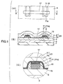
- FIG. 1 shows an area of producing a metal thin-film resistance element according to a first embodiment of a first mode of the present invention, (A) showing a plan view; (B) showing a front elevational sectional view taken along a A-A line of (A); and (C) showing a magnified view of a part defined by a broken line in (B).
- A a passivation film is omitted.
- a transistor device, a capacitance device or such is produced, but is omitted in the figures.
- a device separating oxide film 3 On a silicon substrate 1, a device separating oxide film 3 is produced.
- a wiring pattern 11 made of a metal material pattern 7 and a high-melting-point metal film 9 produced on a surface of the metal material pattern 7 is produced.
- the metal material pattern 7 is made of, for example, an AlSiCu film.
- the high-melting-point metal film 9 is made of, for example, a TiN film, and acts as a reflection preventing film and also as a barrier film.
- Second side walls 15 (omitted in FIG. 1, (A) and (B)) are produced on surfaces of the side walls 13 on the side of the interlayer insulating film 5.
- the second side walls 15 are produced as a result of Ar sputter etching being carried out on the interlayer insulating film 5 after the wiring pattern 11 and the side walls 13 are produced
- the second side walls 15 include Ar as a component, and further include materials of the interlayer insulating film 5, the side walls 13 and the high-melting-point metal film 9
- a belt-shaped CrSi thin-film resistance element (metal thin-film resistance element) 17 is produced on surfaces of the side walls 13, surfaces of the side walls 13 and the interlayer insulating film 5 between a pair of the opposing wiring patterns 11, a belt-shaped CrSi thin-film resistance element (metal thin-film resistance element) 17 is produced. Both end parts of the CrSi thin-film resistance element 17 extend to the surfaces of the side walls 13 and the second walls 15, produced on side surfaces of the pair of the wiring patterns 11 on the side opposite to the side surfaces opposing between the pair of wiring pattern 11, and also extend to the interlayer insulating film 5, as shown.
- the CrSi thin-film resistance element 17 and the wiring patterns 11 intersect each other as shown in FIG. 1, (A). Parts at which the wiring patterns 11 are intersected by the CrSi thin-film resistance element 17 form electrodes 11a.
- the passivation film (omitted in FIG. 1, (A)) is produced on the interlayer insulating film 5 including the area having the CrSi thin-film resistance element 17, and is made of a silicon oxide film 19 on the bottom layer side and a silicon nitride film 21 on the upper layer side.
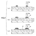
- FIG. 2 shows a process sectional view for illustrating one embodiment of a first aspect of a manufacturing method according to the present invention. This embodiment is applied to manufacture the embodiment of semiconductor device described above with reference to FIG. 1. With reference to FIGS. 1 and 2, the present embodiment of the manufacturing method is described now.
- the CrSi thin-film resistance element 17 is produced over from the top surface of the electrode 11a made of a part of each wiring pattern 11 through the interlayer insulating film 5 via the surfaces of the side walls 13 and 15, it is not necessary to carry out the series of processing to produce the connecting holes which would be carried out in the case where the connecting holes were produced to make electrical connection between the metal thin-film resistance element and the wiring patterns. Accordingly, it is possible to shorten and simplify the manufacturing process. Also, variation of the resistance value of the metal thin-film resistance element and increase of the contact resistance with the electrode do not occur which would otherwise occur due to degradation of step coverage of the metal thin-film resistance element occurring due to existence of the connecting holes.
- both end parts of the CrSi thin-film resistance element 17 extend to intersect the wiring patterns 11 on the electrodes 11a, it is possible to avoid variation of contact areas between the electrodes 11a and the CrSi thin-film resistance element 17 otherwise occurring due to misalignment between the wiring patterns 11 and the CrSi thin-film resistance element 17 or rounding of end parts of the CrSi thin-film resistance element 17. Thus, it is possible to obtain the further stabilized contact resistances.
- the high-melting-point metal film 9 acting as the barrier film is inserted between the CrSi thin-film resistance element 17 and the metal material pattern 7, it is possible to reduce variation of the contact resistance between the CrSi thin-film resistance element 17 and the wiring pattern 11, and thus, it is possible to improve accuracy of the resistance value and the yield.
- the high-melting-point metal film 9 also acts as the reflection preventing film is provided, and also, it is possible to produce the high-melting-point metal film 9 without increasing the number of manufacture processes in comparison to the prior art, it is possible to stabilize the contact resistance between the metal thin-film resistance element and the wiring pattern while preventing increase of the manufacturing cost.
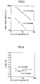
- FIG. 3 shows relationship between a sheet resistance of the metal thin-film resistance element and a film thickness thereof, the ordinate axis denoting the sheet resistance ( ⁇ / ⁇ ) and the abscissa axis denoting the CrSi film thickness ( ⁇ ).
- FIG. 3 shows relationship between a sheet resistance of the metal thin-film resistance element and a film thickness thereof, the ordinate axis denoting the sheet resistance ( ⁇ / ⁇ ) and the abscissa axis denoting the CrSi film thickness ( ⁇ ).
- a condition of producing the thin-film resistance element is as follows:
- Ar sputter etching processing before production of the CrSi thin film was carried out with the use of the above-mentioned multi-chamber sputtering apparatus; in a condition of DC bias: 1250 V; Ar: 20 sccm; pressure: 8.5 milliTorrs; processing time: 160 seconds. This is equivalent to a condition for etching and removing 400 ⁇ of a thermally oxidized film produced in a wet atmosphere at 1000 °C.
- the measurement of the sheet resistance was carried out by a two terminal method in which, twenty belt-shaped patterns each having a width of 0.5 ⁇ m and a length of 50 ⁇ m were arranged with intervals of 0.5 ⁇ m each, and a current value was measured upon applying a voltage of 1V across one metal thin-film resistance element thereof.
- a plan size of each connecting hole connecting between the metal wiring and the CrSi thin-film resistance element was 0.6 ⁇ m by 0.6 ⁇ m.
- the effect obtained from the Ar sputter etching before production of the CrSi thin film is obtained in the same way, not only from a structure in which the metal thin-film resistance element and the wiring pattern are electrically connected via the connecting holes produced in the insulating film on the wiring pattern but also from a structure in which, as in the semiconductor according to the present invention, the wiring pattern and the metal thin-film resistance element are electrically connected on the electrodes made of parts of the wiring patterns.
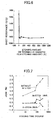
- FIG. 5 shows relationship between the sheet resistance of the CrSi thin-film resistance element both for a case where Ar sputter etching processing was carried out before the metal thin film for the metal thin-film resistance element was produced and for a case where the Ar sputter etching was not carried out, and a time having elapsed after the foundation film of the metal thin-film resistance element was produced.
- FIG. 5, (A) shows the case where the processing was carried out while (B) shows a case where the processing was not carried out.
- the ordinate axis denotes the sheet resistance ( ⁇ / ⁇ ) and the abscissa axis denotes the time having elapsed after the production of the foundation film (hours).
- the plasma SiN film as the foundation film was produced with the use of a parallel plane plate type plasma CVD apparatus, in a condition of temperature: 360 °C; pressure: 5.5 Torrs; RF power: 200 W; SiH 4 : 70 sccm; N 2 : 3500 sccm; NH 3 : 40 sccm.
- the plasma NSG film was produced with the use of a parallel plane plate type plasma CVD apparatus, in a condition of temperature: 400 °C; pressure: 3.0 Torrs; RF power: 250 W; SiH 4 : 16 sccm; N 2 O: 1000 sccm.
- Ar sputter etching was carried out with the use of the above-mentioned multi-chamber sputtering apparatus, in a condition of DC bias: 1250 V; Ar: 20 sccm; pressure: 8.5 milliTorrs; processing time: 80 seconds.
- This condition is equivalent to a condition for etching and removing 200 ⁇ of a thermally oxidized film produced in a wet atmosphere at 1000 °C.
- FIG. 6 shows relationship between an amount of Ar sputter etching and the sheet resistance.
- the ordinate axis denotes the sheet resistance ( ⁇ / ⁇ )
- the abscissa axis denotes the etching amount (expressed by a value translated in a thermally oxidized film etching amount) ( ⁇ ).
- the plasma NSG film and the CrSi thin-film resistance element produced in the same manner as that for the samples of the results of FIG. 5 were applied.
- Ar sputter etching was carried out on the plasma NSG film having elapsed one week after the film production, and after that, the CrSi thin-film resistance element was produced on the NSG film.
- a condition of the Ar sputter etching was the same as that for the samples of FIG. 5 other than the etching amount. Then, adjustment was made for 0 ⁇ (Ar sputter etching was not carried out); 25 ⁇ ; 50 ⁇ ; 100 ⁇ ; 200 ⁇ ; 400 ⁇ ; and 1000 ⁇ in a value translated in an etching amount of a thermally oxidized film produced in wet atmosphere.
- the sheet resistance of the CrSi thin-film resistance element was measured by a four terminal method.
- the samples include only those etched for the film thickness of 1000 ⁇ in a value translated in a thermally oxidized film etching amount as the Ar sputter etching condition.
- FIG. 7 shows relationship between a time for which, after the CrSi thin film was produced, the sample was left in an atmosphere of temperature: 25 °C and humidity: 45%, and a change ratio ( ⁇ R/R0) of the sheet resistance with respect to the value (R0) measured immediately after the film production.
- the ordinate axis denotes ⁇ R/R0 and the abscissa axis denotes the leaving time (hours).
- the resistance value decreased from the film production as a time elapsed, and, after 300 hours has elapsed, the resistance value varied for more than 3 %.
- the Ar sputter etching method is not limited to the DC bias sputter etching method applied currently.
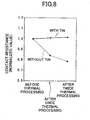
- FIG. 8 shows relationship between variation of the contact resistance between the metal thin-film resistance element and the metal wiring occurring due to thermal processing.
- the ordinate axis denotes a value notarized by the contact resistance value before undergoing thermal processing
- the abscissa axis denotes the number of times of thermal processing.
- the Ar sputter etching processing before production of the CrSi thin film was carried out in a condition of: DC bias: 1250 V; Ar: 20 sccm; pressure: 8.5 milliTorrs; processing time: 160 seconds. This processing corresponding to that for etching and removing 400 ⁇ of thermally oxidized film produced in wet atmosphere at 1000 °C.
- a plan size of each connecting hole was 0.6 ⁇ m by 0.6 ⁇ m.
- a four terminal method was applied for measuring the contact resistance.
- the contact resistance hardly changed, even after the thermal procession was carried out twice, from that before the thermal processing.
- the contact resistance varied by more than 20 % as a result of the twice of the thermal processing being additionally carried out, with respect to that before the thermal processing.
- the TiN film acts as a barrier film for preventing resistance variation otherwise occurring due to interaction between the CrSi thin film and the metal wiring.
- the advantages obtained from inserting the TiN film between the CrSi thin-film resistance element and the metal wiring are obtainable not only from the structure in which the metal thin-film resistance element and the metal wiring are eclectically connected via the connecting holes produced in the insulating film on the wiring pattern but also from a structure in which, as in the semiconductor according to the present invention, the wiring patterns and the metal thin-film resistance element are electrically connected on the electrodes made of parts of the wiring patterns, in the same manner.
- Ar sputter etching processing is carried out immediately before production of the CrSi thin film in the above-mentioned process (3).
- the high-melting-point metal film 9 made of the TiN film does not have a natural oxide film produced thereto not so stiff as that of AlSiCu film even if it is exposed to the atmospheric air. Accordingly, it is possible to obtain an electrical connection between the CrSi thin film and the wiring pattern 11 even without carrying out Ar sputter etching processing. In this case, no side walls 15 are produced.
- the CrSi thin-film resistance element 17 is produced on the interlayer insulating film 5 made of the BPSG film or the PSG film.
- the present invention is not limited to this foundation film used as a foundation of the metal thin-film resistance element.
- an insulating film applied as a foundation of the metal thin-film resistance element another insulating film may be applied, for example, an insulating film having undergone planarization with the use of a CMP (chemical mechanical polish) technology which is a well-known technology, an insulating film having undergone planarization as result of coating of an SOG film, etch back or such, a plasma CVD oxide film not having undergone planarization, or such.
- CMP chemical mechanical polish
- the metal thin-film resistance element included in the semiconductor device according to the present invention is applied as an analog resistance device, it is preferable that the insulating film applied as a foundation of the metal thin-film resistance element has undergone planarization.
- the passivation film 23 is provided on the CrSi thin-film resistance element 17.
- the present invention is not limited to such a structure, and, any insulating film may be applied as a film provided on the CrSi thin-film resistance element 17, for example, an interlayer insulating film for producing metal wiring for a second layer may be applied.
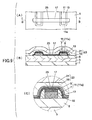
- FIG. 9 shows an area having a metal thin-film resistance element in a second embodiment of the first mode of the semiconductor device according to the present invention.
- FIG. 9, (A) shows a plan view
- FIG. 9, (B) shows a sectional view taken along a B-B position of FIG. 9, (A);
- FIG. 9, (C) shows a magnified view of a portion defined by broken line in FIG. 9, (B).
- a passivation film is omitted.
- the same reference numerals are given to parts having the same functions as those in FIG. 1, and detail description thereof is omitted.
- a device separating oxide film 3 On a silicon substrate 1, a device separating oxide film 3, an interlayer insulating film 5, wiring patterns 11 made of metal material patterns 7 and high-melting-point metal films 9, side walls 13 and second side walls 15 are produced.
- a CrSi thin-film resistance element 17 is produced to intersect a pair of wiring patterns 11 on electrodes 11a, and extend through the interlayer insulating film 5, across the surfaces of the electrodes 11a and the surfaces of the side walls 13 and 15.
- a CrSiN film (metal nitride film) 25 is produced on the top surface of the CrSi thin-film resistance element 17. CrSiO is not produced between the CrSi thin-film resistance element 17 and the CrSiN film 25.
- a passivation film 23 made of a silicon oxide film 19 and a silicon nitride film 21 is produced on all the surface of the interlayer insulating film 5.
- a manufacturing method in an embodiment of a first aspect according to the present invention for producing the semiconductor device in the above-mentioned embodiment shown in FIG. 9 is described next.
- the interlayer insulating film 5 By the same processes (1) and (2) as those described above with reference to FIG. 2, (a) and (b), the interlayer insulating film 5, the wiring patterns 11 made of the metal wiring patterns 7 and the high-melting-point metal films 9, and the side walls 13 are produced on the wafer-shaped silicon substrate 1 on which production of the device separating oxide film 3 is completed.
- a CrSiN film is produced on the CrSi thin-film.
- processing is carried out in a condition of: DC power: 0.7 kW; Ar+N 2 (mixture gas of argon and nitrogen): 85 sccm; pressure: 8.5 milliTorrs; processing time: 6 seconds.
- the CrSiN film is produced on the CrSi thin-film for a film thickness of approximately 50 ⁇ .
- the CrSiN film and the CrSi thin film are patterned, and thus, a laminated pattern made of the CrSiN film 25 and the CrSi thin-film resistance element 17 is produced.
- the CrSi thin-film resistance element 17 is electrically connected with the wiring patterns 11, it is not necessary to carry out metal oxide film removing processing for the surface of the CrSi thin-film resistance element 17 with hydrofluoric solution as in the prior art. Furthermore, since the top surface of the CrSi thin-film resistance element 17 is covered by the CrSiN film 25, the top surface of the CrSi thin-film resistance element 17 can be prevented from being oxidized even when the product is exposed to an atmosphere including oxygen such as the air.
- the passivation film 23 made of the silicon oxide film 19 and the silicon nitride film 21 is produced on the interlayer insulating film 5.
- a metal thin film has a high reactivity to oxygen, and thus, a resistance value thereof changes when it is left exposed to the air for a long duration, as well known.
- the CrSiN film 25 is produced on the top surface of the CrSi thin-film resistance element 17, it is possible to prevent the top surface of the CrSi thin-film resistance element 17b from being directly exposed to the air, and thus, it is possible to prevent the resistance value of the CrSi thin-film resistance element 17 from changing.
- electrical connection between the CrSi thin film and the wiring patterns 11 is already completed in the stage in which the CrSi thin film for producing the CrSi thin-film resistance element 17 has been produced, the performance is never affected even though the new thin film is produced further on the CrSi thin film.
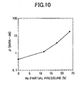
- FIG. 10 shows a relationship between an N 2 partial pressure in a gas for producing the CrSiN film and the resistivity of the CrSiN film.
- the ordinate axis denotes the resistivity ⁇ (mohrm • cm) and the abscissa axis denotes the N 2 partial pressure (%).
- the CrSiN film produced by a reactive sputter with addition of equal to or more than 18 % of N 2 partial pressure has a resistivity higher than that of a case where the gas without addition of N 2 at all (the N 2 partial pressure is 0 %), by equal to or more than ten times. Accordingly, when the CrSiN film is produced with a setting of 18 % or more of the N 2 partial pressure, the overall resistance value of the CrSi thin-film resistance element is substantially determined by the CrSi thin film even when the CrSiN film is produced directly on the CrSi thin-film resistance element. Thus, the CrSiN film hardly affects the resistance value. There, the upper limit of the N 2 partial pressure is on the order of 90 %. If the N 2 partial pressure is set above 90 %, the sputtering speed lowers much, thus production efficiency lowers, and thus, such a setting is not preferable.
- the CrSiN film itself as a metal thin-film resistance element when N 2 partial pressure is added on the order of a range between 6 and 11 %, for example, and the film is produced by a reactive sputter.
- a CVD insulating film for example, a silicon nitride film or such may be produced on the CrSi thin-film resistance element 17 instead.
- a CVD chamber is not connected to a common multi-chamber sputtering apparatus. Accordingly, it is necessary to purchase a corresponding new apparatus for producing such a CVD insulating film on the CrSi thin-film resistance element 17 continuously in vacuo, and thus, the manufacturing cost may be considerably affected.
- FIG. 11 shows an area having a metal thin-film resistance element in a first embodiment of a second mode of the semiconductor device according to the present invention.
- FIG. 11, (A) shows a plan view;
- FIG. 11, (B) shows a sectional view taken along a C-C position of FIG. 11, (A); and
- FIG. 11, (C) shows a magnified view of a portion defined by broken line in FIG. 11, (B).
- a passivation film is omitted.
- the same reference numerals are given to parts having the same functions as those in FIG. 1, and detail description thereof is omitted.
- a device separating oxide film 3 On a silicon substrate 1, a device separating oxide film 3, an interlayer insulating film 5, a wiring pattern 11 made of a metal material pattern 7 and a high-melting-point metal film 9, are produced.
- a second insulating film 31 which is made of a plasma CVD oxide film 27 on a lower layer side and an SOG film 29 on an upper layer side, and is produced to have a metal thickness such as to expose the top surface of the wiring pattern 11 as a result of etch back processing being carried out after the both films are deposited, is produced.
- a belt-shaped CrSi thin-film resistance element 17 is produced on the second insulating film 31 between the opposite pair of wiring patterns 11. Both end parts of the CrSi thin-film resistance element 17 extend over the second insulating films 31 produced in the vicinity of the respective side surfaces of the pair of wiring patterns 11, which side surfaces are those on the other side of the above-mentioned opposite side surfaces of these wiring patterns.
- the CrSi thin-film resistance element 17 and the wiring patterns 11 mutually intersect on electrodes 11a as shown in FIG. 11, (A).
- a passivation film 23 made of a silicon oxide film 19 on a lower layer side and a silicon nitride film 21 on an upper layer side is produced (not shown in FIG. 11, (A)) on the interlayer insulating film 5 including the area having the CrSi thin-film resistance element 17.
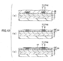
- FIG. 12 shows a process sectional view for illustrating an embodiment of a second aspect of a manufacturing method according to the present invention. This embodiment is applied to manufacture the semiconductor device described above with reference to FIG. 11. With reference to FIGS. 11 and 12, the present embodiment is described now.
- the second insulating film 31 is produced on the side surfaces of the wiring patterns, degradation of step coverage of the CrSi thin-film resistance element 17 due to steep steps at the side surfaces of the wiring patterns can be avoided.
- both end parts of the CrSi thin-film resistance element 17 extend to intersect the wiring patterns 11 on the electrodes 11a, it is possible to avoid variation of contact areas between the electrodes 11a and the CrSi thin-film resistance element 17 otherwise occurring due to misalignment between the wiring patterns 11 and the CrSi thin-film resistance element 17 or rounding of end parts of the CrSi thin-film resistance element 17. Thus, it is possible to obtain the further stabilized contact resistance.
- the high-melting-point metal film 9 acting as the barrier film is inserted between the CrSi thin-film resistance element 17 and the metal material pattern 7, it is possible to reduce variation of the contact resistance between the CrSi thin-film resistance element 17 and the wiring pattern 11, and thus, it is possible to improve accuracy of the resistance value and the yield.
- the high-melting-point metal film 9 also acts as the reflection preventing film and also, it is possible to produce the high-melting-point metal film 9 without increasing the number of manufacture processes in comparison to the prior art, it is possible to stabilize the contact resistance between the metal thin-film resistance element and the wiring pattern while preventing increase of the manufacturing cost.
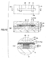
- FIG. 13 shows an area having a metal thin-film resistance element in a second embodiment of the second mode of the semiconductor device according to the present invention.
- FIG. 13, (A) shows a plan view
- FIG. 13, (B) shows a sectional view taken along a D-D position
- FIG. 13, (C) shows a magnified view of a portion defined by broken line in FIG. 13, (B).
- a passivation film is omitted.
- the same reference numerals are given to parts having the same functions as those in FIG. 1, and detail description thereof is omitted.
- a device separating oxide film 3 On a silicon substrate 1, a device separating oxide film 3, an interlayer insulating film 5, wiring patterns 11 each made of a metal material pattern 7 and a high-melting-point metal film 9, and a second insulating film 31 made of a plasma CVD oxide film 27 and an SOG film 29 are produced.
- a CrSi thin-film resistance element 17 is produced to intersect a pair of wiring patterns 11 on electrodes 11a, and extend over the second insulating film 31 across the surfaces of the electrodes 11a.
- a CrSiN film 25 is produced on the top surface of the CrSi thin-film resistance element 17. CrSiO is not produced between the CrSi thin-film resistance element 17 and the CrSiN film 25.
- a passivation film 23 made of a silicon oxide film 19 and a silicon nitride film 21 is produced on all the surface of the second insulating film 31.
- the interlayer insulating film 5, the wiring patterns 11 made of the metal wiring patterns 7 and the high-melting-point metal films 9, and the second insulating film 31 made of the plasma CVD oxide film 27 and the SOG film 29 are produced on the wafer-shaped silicon substrate 1 on which production of the device separating oxide film 3 is completed.
- the CrSiN film and the CrSi thin film are patterned, and thus, a laminated pattern made of the CrSiN film 25 and the CrSi thin-film resistance element 17 is produced.
- a passivation film 23 made of the silicon oxide film 19 and the silicon nitride film 21 is produced on the second insulating film 31
- the CrSiN film 25 is produced on the top surface of the CrSi thin-film resistance element 17, it is possible to prevent the top surface of the CrSi thin-film resistance element 17 from being exposed to the air, and thus, it is possible to prevent the resistance value of the CrSi thin-film resistance element 17 from changing.
- the second insulating film 31 one obtained as a result of the SOG film 29 being coated on the plasma CVD oxide film 27, and the SOG film 29 being then planarized as a result of etch back processing being carried out thereon is applied.
- the second insulating film which acts as a foundation of the metal thin-film resistance element 17 is not limited thereto.
- an HDP high-density-plasma
- a deposited plasma CVD oxide film being polished to have a film thickness such as to expose surfaces of the wiring patterns by means of a CMP method or such may be applied instead.
- the example where the TiN film is applied as the high-melting-point metal film 9 is shown.
- the high-melting-point metal film included in each of the wiring patterns is not limited thereto.
- another material such as TiW, WSi or such may be applied as the high-melting-point metal film instead.
- the present invention is applied to the semiconductor device in which the single layer of the wiring patterns 11 are provided as metal wiring.
- the present invention is not limited thereto, and, the present invention may be applied to a semiconductor device having a multi-layer metal wiring structure.
- a metal wiring under the metal thin-film resistance element for making electrical connection from the metal thin-film resistance element may correspond to a metal wiring of any layer of the plurality of layers of metal wiring.
- the wiring pattern (metal wiring) under the metal thin-film resistance element that is, the wiring pattern for making electrical connection from the metal thin-film resistance element corresponds to the wiring pattern of the top layer of the plurality of layers of metal wiring
- layout change of the metal thin-film resistance element can be achieved by layout change of the metal thin-film resistance element and the top layer wiring pattern.
- a final protection film made of an insulating material is produced on the metal thin-film resistance element.
- each wiring pattern 11 one in which the high-melting-point metal film 9 is produced on the wiring material pattern 7 is applied.
- the present invention is not limited thereto, and, as the wiring pattern, a metal material pattern having no high-melting-point metal film produced on the top thereof may be applied instead.
- Al alloy is applied as the metal material pattern, a stiff natural oxide film is produced on the surface of the metal material pattern. Therefore, it is preferable to carry out a process of removing the natural oxide film from the surface of the metal material pattern, before producing the metal thin film for the metal thin-film resistance element.
- This natural oxide film removing process may be carried out as common processing as the above-mentioned Ar sputtering processing for the purpose of reducing aging variation of the resistance value of the metal thin-film resistance element.
- the wiring pattern is not limited to the Al alloy, and a wiring pattern made of another metal material such as a Cu wiring produced by a so-called damascene processing or such may be applied for example, instead.
- the wiring pattern to obtain an electric potential of the CrSi thin-film resistance element 17 one made of the metal material pattern 7 and the high-melting-point metal film 9 is applied.
- a polysilicon pattern instead of the metal material pattern 7, a polysilicon pattern may be applied
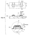
- FIG. 14 shows an area having a metal thin-film resistance element according to a third embodiment of the first mode according to the present invention, (A) showing a plan view; (B) showing a front elevational sectional view taken along a E-E line of (A); and (C) showing a magnified view of a part defined by a broken line in (B).
- (A) a passivation film is omitted.
- the same reference numerals are given to parts having the same functions as those shown in FIG. 1, and detailed description thereof is omitted.
- a device separating oxide film 3 is produced on a silicon substrate 1.
- a device separating oxide film 3 is produced on an oxide film (not shown) produced on the polysilicon substrate 1 and on the device separating oxide film 3, wiring patterns 27 made of polysilicon patterns 33 and high-melting-point metal films 35 produced on the polysilicon patterns 33 respectively are produced.
- the high-melting-point metal film 35 is made of, for example, WSi or TiSi.
- the wiring pattern 37 forms a gate electrode.
- Second side walls 41 (omitted in FIG. 14, (A) and (B)) are produced on surfaces of the side walls 39 on the side of the device separating oxide film 3.
- the second side walls 41 are produced as a result of Ar sputter etching being carried out on the device separating oxide film 3 after the wiring patterns 37 and the side walls 39 are produced.
- the second side walls 41 include Ar as a component, and further include materials of the device separating oxide film 3, the side walls 39 and the high-melting-point metal film 35.
- a belt-shaped CrSi thin-film resistance element (metal thin-film resistance element) 17 is produced on surfaces of the side walls 39 between the pair of opposing wiring patterns 37. Both end parts of the CrSi thin-film resistance element 17 extend over surfaces of the side walls 39 and the second side walls 41 produced on the side surfaces on the respective sides opposite to the side surfaces opposing between the pair of wiring pattern 37, and also extend over the device separating oxide film 3.
- the CrSi thin-film resistance element 17 and the wiring patterns 37 intersect each other. Parts at which the wiring patterns 37 are intersected by the CrSi thin-film resistance element 17 form electrodes 37a (see FIG. 14, (A)) .
- an interlayer insulating film, a metal wiring pattern and a passivation film are produced on the device separating oxide film interlayer film 3 including the areas having the CrSi thin-film resistance element 17, the wiring patterns 37, and the side walls 39 and 41.
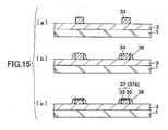
- FIG. 15 shows a process sectional view for illustrating a second embodiment of the first aspect of a manufacturing method according to the present invention. This embodiment is applied to manufacture the embodiment of semiconductor device described above with reference to FIG. 14. With reference to FIGS. 14 and 15, the embodiment of the manufacturing method is described.
- the high-melting-point metal film 35 acting as the barrier film is inserted between the CrSi thin-film resistance element 17 and the polysilicon pattern 33, it is possible to reduce variation of the contact resistance between the CrSi thin-film resistance element 17 and the wiring pattern 37, and thus, it is possible to improve accuracy of the resistance value and the yield.
- the high-melting-point metal film 35 also contributes to resistance reduction of the polysilicon patterns 33, also it is possible to produce the high-melting-point metal film 35 without increasing the number of manufacture processes in comparison to the prior art, and it is possible to stabilize the contact resistance between the metal thin-film resistance element and the wiring pattern while preventing increased of the manufacturing costs.
- a transistor device having an LDD (lightly doped drain) structure such as a transistor device having a side wall on a side surface of a polysilicon pattern forming a gate electrode is produced on the common silicon substrate
- LDD lightly doped drain
- LDD lightly doped drain
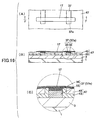
- FIG. 16 shows an area having a metal thin-film resistance element according to a third embodiment of the second mode according to the present invention, (A) showing a plan view; (B) showing a front elevational sectional view taken along a F-F line of (A); and (C) showing a magnified view of a part defined by a broken line in (B).
- (A) a passivation film is omitted.
- the same reference numerals are given to parts having the same functions as those shown in FIG. 1 and FIG. 14, and detailed description thereof is omitted.
- a device separating oxide film 3 and wiring patterns 37 each made of polysilicon patterns 33 and high-melting-point metal films 35 are produced.
- a belt-shaped CrSi thin-film resistance element 17 is produced on the second insulting film 47 between the opposite pair of wiring patterns 37. Both end parts of the CrSi thin-film resistance element 17 extend over the second insulating film 47 produced in the vicinity of the side surfaces of the pair of wiring patterns 37, which side surfaces are located opposite to the side surfaces of the pair wiring patterns 37 opposing one another, and the CrSi thin-film resistance element 17 and the wiring patterns 37 intersect each other at electrodes 37a.
- an interlayer insulating film, a metal wiring pattern and passivation film are produced on the second insulating films 47 including the areas in which the CrSi thin-film resistance element 17 and the wiring patterns 37 are produced.
- FIG. 17 shows a process sectional view for illustrating a fourth embodiment of the second aspect of a manufacturing method according to the present invention. This embodiment is applied to manufacture the embodiment of semiconductor device described above with reference to FIG. 16. With reference to FIGS. 16 and 17, the embodiment of the manufacturing method is described.
- the interlayer insulating film, the metal wiring pattern, the passivation film and so forth are produced.
- the advantage obtained as a result of the high-melting-point metal film 35 acting as the barrier film being inserted between the CrSi thin-film resistance element 17 and the polysilicon pattern 33, the advantage obtained as a result of the high-melting-point metal film 35 contributing resistance reduction of the polysilicon patterns 33, and the advantage obtained from the Ar sputter etch being carried out before the metal thin film for the CrSi thin-film resistance element is produced, are also obtained.
- the second insulating film 47 produced to have the film thickness to expose the surfaces of the wiring patterns 37 on the device separating oxide film 3 has an effect to omit or reduce planarization processing carried out on the interlayer insulating film produced over the second insulating film 47.
- the CrSiN film may be produced on the CrSi thin-film resistance element 17, the same as in the embodiment described above with reference to FIG. 9 and the embodiment described with reference to FIG. 13.
- the CrSi thin-film resistance element 17 and the wiring patterns 11 or 37 intersect each other.
- the present invention is not limited thereto.
- Merely end parts of the metal thin-film resistance element may be disposed on the wiring patterns, or end parts of the wiring patterns may be deposed below the metal thin-film resistance element.
- end parts of the CrSi thin-film resistance element 17 may be disposed on the wiring patterns 11.
- end parts of the wiring patterns 11 may be disposed below the CrSi thin-film resistance element 17.
- the metal thin-film resistance element should not be necessarily disposed to extend perpendicular to the wiring patterns. Shapes, directions and arrangements of the metal thin-film resistance element and the wiring patterns are not limited to the embodiments. For example, as shown in a plan view shown in FIG. 19, (A) or (B), the metal thin-film resistance element and the wiring patterns may be disposed in mutually parallel relationship.
- CrSi is applied as material of the metal thin-film resistance element.
- the present invention is not limited thereto.
- another material may be applied, for example, NiCr, TaN, CrSi 2 , CrSiN, CrSi, CrSiO or such.
- a metal thin-film resistance element included in a semiconductor device according to the present invention, or a metal thin-film resistance element produced according to a manufacturing method according to the present invention may be applied to a semiconductor device having an analog circuit, for example.
- Embodiments of a semiconductor device having an analog circuit applying a metal thin-film resistance element according to the present invention are described next.
- FIG. 20 shows a circuit diagram of one embodiment of a semiconductor device including an analog circuit, i.e., a constant voltage generating circuit.
- the constant voltage generating circuit 55 includes an input terminal (Vbat) 57 to which the direct-current power source is connected; a reference voltage generating circuit (Vref) 59, an operational amplifier (comparison circuit) 61; a P-channel MOS transistor (abbreviated as PMOS, hereinafter) acting as an output driver; dividing resistance devices R1, R2; and an output terminal (Vout) 65.
- Vbat input terminal
- Vref reference voltage generating circuit
- PMOS P-channel MOS transistor
- an output terminal is connected to a gate electrode of the PMOS 63; a reference voltage Vref is applied to an inverted input terminal (-) by the reference voltage generating circuit 59; a voltage divided by the resistance elements R1 and R2 is applied to the non-inverted input terminal (+); and thus, control is made such that the R1 and R2 divided voltage may become equal to the reference voltage Vref.
- FIG. 21 shows a circuit diagram showing another embodiment of a semiconductor device including an analog circuit, i.e., a voltage detecting circuit.
- a reference voltage generating circuit 59 is connected to an inverted input terminal (-) of an operational amplifier 61, and thus, a reference voltage Vref is applied thereto.
- a voltage input via an input terminal (Vsens) 69 to be measured is divided by dividing resistance elements R1 and R2, and then, is applied to a non-inverted input terminal (+).
- An output of the operational amplifier 61 is output externally via an output terminal (Vout) 71.
- the operational amplifier 61 maintains an H level in its output.
- the operational amplifier 61 maintains an L level.
- the reference voltage Vref from the reference voltage generating circuit may vary due to a variation of a manufacturing process.
- the resistance values of the dividing resistance elements may be adjusted as a result of applying, as each dividing resistance element, a resistance element circuit (referred to as a dividing resistance circuit) in which a resistance value is adjustable as a result of a fuse of a fuse element being brown.
- FIG. 22 shows one example of the dividing resistance circuit to which a metal thin-film resistance element according to the present invention is applicable
- FIG. 23 and FIG. 24 show layout diagrams showing layouts in the dividing resistance circuit.
- FIG. 23 shows an example of a layout of a fuse element part.
- FIG. 24 shows an example of a layout of a resistance element part.
- a resistance element Rbottom, m+1 (m denoting a positive integer) resistance elements RT0, RT1, RT2, ..., RTm, and a resistance element Rtop are connected in series.
- m+1 (m denoting a positive integer) resistance elements RT0, RT1, RT2, ..., RTm, and a resistance element Rtop are connected in series.
- a respective one of fuse elements RL0, RL1, ..., RLm is connected in parallel.
- each of the fuse elements RL0, RL1, ..., RLm is produced of a polysilicon pattern having a sheet resistance in a range between 20 ⁇ and 40 ⁇ .
- Resistance values of the resistance elements RT0, RT1, ..., RTm are set to increase in a manner of a binary notation from the side of the resistance element Rbottom. That is, each resistance element RTn has a resistance value which is 2° times a resistance value (regarded as a unit value) of the resistance element RT0.
- the resistance element RT0 is made of the single CrSi thin-film resistance element 17 as a unit resistance; and each resistance element RTn is made of the 2 n CrSi thin-film resistance elements 17.
- respective electrical connections are provided between reference signs A-A; between reference signs B-B; between reference signs C-C; between reference signs D-D; between reference signs E-E; between reference signs F-F; and between reference signs G-G, by metal wiring pattern.
- unit resistance elements each including a pair of the resistance element and the fuse element are disposed in a manner of a ladder (see FIG. 22).
- any of the fuse elements RL0, RL1, ..., RLm may be brown by a laser beam, and thus a desired series resistance value is obtainable.
- the end terminal of the resistance element Rbottom is grounded, and the end terminal of the resistance element Rtop is connected to the drain of the PMOS 71, for example. Further, the terminal NodeL between the resistance elements Rbottom and RT0 or the terminal NodeM between the resistance elements Rtop and RTm is connected to the non-inverted input terminal of the operational amplifier 61.
- the accuracy of the output voltage of the dividing resistance elements R1 and R1 can be improved as a result of the dividing resistance circuit in which the metal thin-film resistance elements according to the present invention are applied being applied, it is possible to improve stabilization of the output voltage of the constant voltage generating circuit. Further, as a result of the area required to produce the dividing resistance circuit being able to be reduced, the area required to produce the constant voltage generating circuit 55 can be reduced accordingly.
- the end terminal of the resistance element Rbottom is grounded, and the end terminal of the resistance element Rtop is connected to the input terminal 77, for example. Further, the terminal NodeL between the resistance elements Rbottom and RT0 or the terminal NodeM between the resistance elements Rtop and RTm is connected to the non-inverted input terminal of the operational amplifier 61.
- the accuracy of the output voltage of the dividing resistance elements R1 and R1 can be improved as a result of the dividing resistance circuit in which the metal thin-film resistance elements according to the present invention are applied being applied, it is possible to improve the accuracy of the voltage detecting capability of the voltage detecting circuit 67. Further, as a result of the area required to produce the dividing resistance circuit being reduced, the area required to produce the voltage detecting circuit 67 can be reduced accordingly.
- a semiconductor device in which the dividing resistance circuit in which the metal thin-film resistance elements according to the present invention are applicable is not limited to the semiconductor device including the constant voltage generating circuit or the semiconductor device including the voltage detecting circuit. It can be applied also to any other semiconductor circuit including the dividing resistance circuit. Further, a semiconductor device in which the metal thin-film resistance element is applicable is not limited to the semiconductor device including the dividing resistance circuit. It can be applied also to any other semiconductor device including the metal thin-film resistance element. For example, a metal thin-film resistance element may be applied as a resistance element applied to adjust a resistance value as a result of laser light being applied to the resistance element itself so as to cut or alter the quality thereof.
Landscapes
- Semiconductor Integrated Circuits (AREA)
- Internal Circuitry In Semiconductor Integrated Circuit Devices (AREA)
Applications Claiming Priority (2)
| Application Number | Priority Date | Filing Date | Title |
|---|---|---|---|
| JP2004040910A JP4610205B2 (ja) | 2004-02-18 | 2004-02-18 | 半導体装置 |
| JP2004040910 | 2004-02-18 |
Publications (2)
| Publication Number | Publication Date |
|---|---|
| EP1566831A2 true EP1566831A2 (fr) | 2005-08-24 |
| EP1566831A3 EP1566831A3 (fr) | 2009-02-25 |
Family
ID=34709087
Family Applications (1)
| Application Number | Title | Priority Date | Filing Date |
|---|---|---|---|
| EP05250899A Withdrawn EP1566831A3 (fr) | 2004-02-18 | 2005-02-17 | Dispositif a semi-conducteurs et procédé de fabrication dudit dispositif |
Country Status (3)
| Country | Link |
|---|---|
| US (1) | US20050212085A1 (fr) |
| EP (1) | EP1566831A3 (fr) |
| JP (1) | JP4610205B2 (fr) |
Cited By (1)
| Publication number | Priority date | Publication date | Assignee | Title |
|---|---|---|---|---|
| EP2423949A3 (fr) * | 2010-08-24 | 2013-05-01 | STMicroelectronics Pte Ltd. | Résistance à film mince multicouche sans trou d'interconnexion et sa procédé de fabrication |
Families Citing this family (10)
| Publication number | Priority date | Publication date | Assignee | Title |
|---|---|---|---|---|
| JP4665631B2 (ja) * | 2005-07-07 | 2011-04-06 | セイコーエプソン株式会社 | 電子基板とその製造方法及び電気光学装置の製造方法並びに電子機器の製造方法 |
| JP4419926B2 (ja) * | 2005-07-14 | 2010-02-24 | セイコーエプソン株式会社 | 半導体装置 |
| JP4841220B2 (ja) * | 2005-10-14 | 2011-12-21 | 株式会社リコー | 半導体装置 |
| DE102006056777B4 (de) * | 2006-12-01 | 2013-10-10 | Infineon Technologies Ag | Zusammenstellung umfassend ein Trägerelement mit einer Abschirmschicht und einen Chip |
| JP2008226963A (ja) * | 2007-03-09 | 2008-09-25 | Hitachi Ltd | 半導体装置及びその製造方法 |
| JP5616822B2 (ja) * | 2011-03-03 | 2014-10-29 | セイコーインスツル株式会社 | 半導体装置の製造方法 |
| CN103187323A (zh) * | 2011-12-28 | 2013-07-03 | 北大方正集团有限公司 | 一种半导体芯片及其压焊块金属层增厚制作方法 |
| JP6120528B2 (ja) * | 2012-11-08 | 2017-04-26 | ルネサスエレクトロニクス株式会社 | 半導体装置およびその製造方法 |
| JP6075114B2 (ja) | 2013-02-27 | 2017-02-08 | ローム株式会社 | 半導体装置および半導体装置の製造方法 |
| US20180269270A1 (en) * | 2017-03-14 | 2018-09-20 | Ablic Inc. | Semiconductor device |
Citations (7)
| Publication number | Priority date | Publication date | Assignee | Title |
|---|---|---|---|---|
| JPS58148443A (ja) | 1982-03-01 | 1983-09-03 | Seiko Epson Corp | 半導体集積回路装置 |
| JPS61100956A (ja) | 1984-10-22 | 1986-05-19 | Nec Corp | モノブリツド集積回路 |
| JP2699559B2 (ja) | 1989-06-29 | 1998-01-19 | 富士通株式会社 | 半導体装置の製造方法 |
| JP2932940B2 (ja) | 1994-06-08 | 1999-08-09 | 株式会社デンソー | 薄膜抵抗体を有する半導体装置の製造方法 |
| JP3185677B2 (ja) | 1996-08-12 | 2001-07-11 | 株式会社デンソー | 高融点金属を用いた半導体装置の製造方法 |
| JP2002124639A (ja) | 2000-08-09 | 2002-04-26 | Seiko Instruments Inc | 半導体装置及びその製造方法 |
| JP2002261237A (ja) | 2001-02-27 | 2002-09-13 | Sony Corp | 半導体装置及びその製造方法 |
Family Cites Families (24)
| Publication number | Priority date | Publication date | Assignee | Title |
|---|---|---|---|---|
| JP2601933B2 (ja) * | 1990-04-13 | 1997-04-23 | 株式会社東芝 | 固体撮像装置 |
| JPH0444260A (ja) * | 1990-06-08 | 1992-02-14 | Fujitsu Ltd | 半導体装置の製造方法 |
| KR940008883B1 (ko) * | 1992-04-08 | 1994-09-28 | 삼성전자 주식회사 | 박막저항의 제조방법 |
| US5308795A (en) * | 1992-11-04 | 1994-05-03 | Actel Corporation | Above via metal-to-metal antifuse |
| JPH06291258A (ja) * | 1993-04-07 | 1994-10-18 | Oki Electric Ind Co Ltd | 薄膜抵抗の形成方法 |
| US5367284A (en) * | 1993-05-10 | 1994-11-22 | Texas Instruments Incorporated | Thin film resistor and method for manufacturing the same |
| US5496771A (en) * | 1994-05-19 | 1996-03-05 | International Business Machines Corporation | Method of making overpass mask/insulator for local interconnects |
| US6034411A (en) * | 1997-10-29 | 2000-03-07 | Intersil Corporation | Inverted thin film resistor |
| JP3134927B2 (ja) * | 1998-05-01 | 2001-02-13 | 日本電気株式会社 | 半導体装置及びsramセルの製造方法 |
| US6555455B1 (en) * | 1998-09-03 | 2003-04-29 | Micron Technology, Inc. | Methods of passivating an oxide surface subjected to a conductive material anneal |
| JP2000113428A (ja) * | 1998-10-08 | 2000-04-21 | Tdk Corp | 薄膜デバイス、薄膜磁気ヘッドおよび磁気抵抗効果素子並びにそれらの製造方法 |
| US6316325B1 (en) * | 1998-11-13 | 2001-11-13 | United Microelectronics Corp. | Method for fabricating a thin film resistor |
| JP2000332203A (ja) * | 1999-05-17 | 2000-11-30 | Hitachi Ltd | 半導体装置およびその製造方法 |
| US6255703B1 (en) * | 1999-06-02 | 2001-07-03 | Advanced Micro Devices, Inc. | Device with lower LDD resistance |
| US20010017397A1 (en) * | 1999-06-11 | 2001-08-30 | Jia-Sheng Lee | Thin-film resistor and method of fabrication |
| US6140192A (en) * | 1999-06-30 | 2000-10-31 | United Microelectronics Corp. | Method for fabricating semiconductor device |
| US6303503B1 (en) * | 1999-10-13 | 2001-10-16 | National Semiconductor Corporation | Process for the formation of cobalt salicide layers employing a sputter etch surface preparation step |
| JP2001237422A (ja) * | 1999-12-14 | 2001-08-31 | Sanyo Electric Co Ltd | 半導体装置およびその製造方法 |
| AU2001296281A1 (en) * | 2000-09-21 | 2002-04-02 | Michaeld. Casper | Integrated thin film capacitor/inductor/interconnect system and method |
| US6483154B1 (en) * | 2000-10-05 | 2002-11-19 | Advanced Micro Devices, Inc. | Nitrogen oxide plasma treatment for reduced nickel silicide bridging |
| US6432805B1 (en) * | 2001-02-15 | 2002-08-13 | Advanced Micro Devices, Inc. | Co-deposition of nitrogen and metal for metal silicide formation |
| US6689658B2 (en) * | 2002-01-28 | 2004-02-10 | Silicon Based Technology Corp. | Methods of fabricating a stack-gate flash memory array |
| US7473947B2 (en) * | 2002-07-12 | 2009-01-06 | Intel Corporation | Process for ultra-thin body SOI devices that incorporate EPI silicon tips and article made thereby |
| US6975006B2 (en) * | 2003-07-25 | 2005-12-13 | Taiwan Semiconductor Manufacturing Company | Semiconductor device with modified channel compressive stress |
-
2004
- 2004-02-18 JP JP2004040910A patent/JP4610205B2/ja not_active Expired - Fee Related
-
2005
- 2005-02-17 EP EP05250899A patent/EP1566831A3/fr not_active Withdrawn
- 2005-02-17 US US11/059,725 patent/US20050212085A1/en not_active Abandoned
Patent Citations (7)
| Publication number | Priority date | Publication date | Assignee | Title |
|---|---|---|---|---|
| JPS58148443A (ja) | 1982-03-01 | 1983-09-03 | Seiko Epson Corp | 半導体集積回路装置 |
| JPS61100956A (ja) | 1984-10-22 | 1986-05-19 | Nec Corp | モノブリツド集積回路 |
| JP2699559B2 (ja) | 1989-06-29 | 1998-01-19 | 富士通株式会社 | 半導体装置の製造方法 |
| JP2932940B2 (ja) | 1994-06-08 | 1999-08-09 | 株式会社デンソー | 薄膜抵抗体を有する半導体装置の製造方法 |
| JP3185677B2 (ja) | 1996-08-12 | 2001-07-11 | 株式会社デンソー | 高融点金属を用いた半導体装置の製造方法 |
| JP2002124639A (ja) | 2000-08-09 | 2002-04-26 | Seiko Instruments Inc | 半導体装置及びその製造方法 |
| JP2002261237A (ja) | 2001-02-27 | 2002-09-13 | Sony Corp | 半導体装置及びその製造方法 |
Cited By (1)
| Publication number | Priority date | Publication date | Assignee | Title |
|---|---|---|---|---|
| EP2423949A3 (fr) * | 2010-08-24 | 2013-05-01 | STMicroelectronics Pte Ltd. | Résistance à film mince multicouche sans trou d'interconnexion et sa procédé de fabrication |
Also Published As
| Publication number | Publication date |
|---|---|
| JP4610205B2 (ja) | 2011-01-12 |
| US20050212085A1 (en) | 2005-09-29 |
| EP1566831A3 (fr) | 2009-02-25 |
| JP2005235888A (ja) | 2005-09-02 |
Similar Documents
| Publication | Publication Date | Title |
|---|---|---|
| US7615844B2 (en) | Semiconductor device | |
| JP5146504B2 (ja) | 半導体装置の製造方法 | |
| US7718502B2 (en) | Semiconductor apparatus including a thin-metal-film resistor element and a method of manufacturing the same | |
| US7358592B2 (en) | Semiconductor device | |
| US6081014A (en) | Silicon carbide chrome thin-film resistor | |
| JP4776199B2 (ja) | 半導体装置の製造方法 | |
| EP1566831A2 (fr) | Dispositif a semi-conducteurs et procédé de fabrication dudit dispositif | |
| JP4549075B2 (ja) | 半導体装置及びその製造方法 | |
| JP4322732B2 (ja) | 定電流発生回路 | |
| US7956672B2 (en) | Reference voltage generating circuit | |
| JP4675050B2 (ja) | 半導体装置 | |
| JP2005317948A (ja) | 基準電圧発生回路 | |
| JP4484548B2 (ja) | 半導体装置 | |
| JP4137040B2 (ja) | 半導体装置の製造方法 | |
| JP2005268749A (ja) | 半導体装置 | |
| JP4497975B2 (ja) | 半導体装置 | |
| JP2006190806A (ja) | 半導体装置の製造方法 |
Legal Events
| Date | Code | Title | Description |
|---|---|---|---|
| PUAI | Public reference made under article 153(3) epc to a published international application that has entered the european phase |
Free format text: ORIGINAL CODE: 0009012 |
|
| 17P | Request for examination filed |
Effective date: 20050228 |
|
| AK | Designated contracting states |
Kind code of ref document: A2 Designated state(s): AT BE BG CH CY CZ DE DK EE ES FI FR GB GR HU IE IS IT LI LT LU MC NL PL PT RO SE SI SK TR |
|
| AX | Request for extension of the european patent |
Extension state: AL BA HR LV MK YU |
|
| RIC1 | Information provided on ipc code assigned before grant |
Ipc: H01L 23/525 20060101ALI20080929BHEP Ipc: H01L 21/02 20060101AFI20050518BHEP Ipc: H01L 23/522 20060101ALN20080929BHEP Ipc: H01L 27/01 20060101ALN20080929BHEP Ipc: H01L 27/08 20060101ALI20080929BHEP |
|
| PUAL | Search report despatched |
Free format text: ORIGINAL CODE: 0009013 |
|
| AK | Designated contracting states |
Kind code of ref document: A3 Designated state(s): AT BE BG CH CY CZ DE DK EE ES FI FR GB GR HU IE IS IT LI LT LU MC NL PL PT RO SE SI SK TR |
|
| AX | Request for extension of the european patent |
Extension state: AL BA HR LV MK YU |
|
| 17Q | First examination report despatched |
Effective date: 20090609 |
|
| AKX | Designation fees paid |
Designated state(s): DE ES FR GB IT NL |
|
| STAA | Information on the status of an ep patent application or granted ep patent |
Free format text: STATUS: THE APPLICATION IS DEEMED TO BE WITHDRAWN |
|
| 18D | Application deemed to be withdrawn |
Effective date: 20110901 |