EP1562231A2 - Electro-optical device and electronic device - Google Patents
Electro-optical device and electronic device Download PDFInfo
- Publication number
- EP1562231A2 EP1562231A2 EP05010071A EP05010071A EP1562231A2 EP 1562231 A2 EP1562231 A2 EP 1562231A2 EP 05010071 A EP05010071 A EP 05010071A EP 05010071 A EP05010071 A EP 05010071A EP 1562231 A2 EP1562231 A2 EP 1562231A2
- Authority
- EP
- European Patent Office
- Prior art keywords
- tft
- film
- display device
- gate
- layer
- Prior art date
- Legal status (The legal status is an assumption and is not a legal conclusion. Google has not performed a legal analysis and makes no representation as to the accuracy of the status listed.)
- Granted
Links
- 239000000463 material Substances 0.000 claims description 101
- 239000000758 substrate Substances 0.000 claims description 40
- 239000011368 organic material Substances 0.000 claims description 11
- 239000000853 adhesive Substances 0.000 claims description 10
- 230000001070 adhesive effect Effects 0.000 claims description 10
- 239000010409 thin film Substances 0.000 claims description 10
- 239000011521 glass Substances 0.000 claims description 9
- 239000002274 desiccant Substances 0.000 claims description 4
- 239000007788 liquid Substances 0.000 claims description 4
- 239000003822 epoxy resin Substances 0.000 claims description 3
- 239000011261 inert gas Substances 0.000 claims description 3
- 229920000647 polyepoxide Polymers 0.000 claims description 3
- 238000002347 injection Methods 0.000 abstract description 9
- 239000007924 injection Substances 0.000 abstract description 9
- 230000009467 reduction Effects 0.000 abstract description 5
- 230000002265 prevention Effects 0.000 abstract 1
- 239000010408 film Substances 0.000 description 257
- 239000010410 layer Substances 0.000 description 136
- 238000000034 method Methods 0.000 description 42
- 238000002161 passivation Methods 0.000 description 38
- 239000012535 impurity Substances 0.000 description 30
- 238000010586 diagram Methods 0.000 description 26
- 229910052710 silicon Inorganic materials 0.000 description 26
- XUIMIQQOPSSXEZ-UHFFFAOYSA-N Silicon Chemical compound [Si] XUIMIQQOPSSXEZ-UHFFFAOYSA-N 0.000 description 24
- 239000011229 interlayer Substances 0.000 description 24
- 239000010703 silicon Substances 0.000 description 24
- 238000004519 manufacturing process Methods 0.000 description 20
- 239000003990 capacitor Substances 0.000 description 18
- 229910052751 metal Inorganic materials 0.000 description 17
- 239000002184 metal Substances 0.000 description 17
- 239000011159 matrix material Substances 0.000 description 14
- 239000000203 mixture Substances 0.000 description 14
- 150000001875 compounds Chemical class 0.000 description 13
- 238000003475 lamination Methods 0.000 description 13
- 230000008569 process Effects 0.000 description 13
- 239000011347 resin Substances 0.000 description 13
- 229920005989 resin Polymers 0.000 description 13
- 239000004065 semiconductor Substances 0.000 description 13
- 239000012298 atmosphere Substances 0.000 description 12
- 230000015572 biosynthetic process Effects 0.000 description 12
- 229910052799 carbon Inorganic materials 0.000 description 12
- 239000000126 substance Substances 0.000 description 12
- OKTJSMMVPCPJKN-UHFFFAOYSA-N Carbon Chemical compound [C] OKTJSMMVPCPJKN-UHFFFAOYSA-N 0.000 description 11
- 238000001994 activation Methods 0.000 description 11
- 229910052782 aluminium Inorganic materials 0.000 description 11
- 229910021419 crystalline silicon Inorganic materials 0.000 description 11
- 230000005855 radiation Effects 0.000 description 11
- IJGRMHOSHXDMSA-UHFFFAOYSA-N Atomic nitrogen Chemical compound N#N IJGRMHOSHXDMSA-UHFFFAOYSA-N 0.000 description 10
- -1 aluminum nitride compound Chemical class 0.000 description 10
- 238000002425 crystallisation Methods 0.000 description 10
- 230000006866 deterioration Effects 0.000 description 10
- BHEPBYXIRTUNPN-UHFFFAOYSA-N hydridophosphorus(.) (triplet) Chemical compound [PH] BHEPBYXIRTUNPN-UHFFFAOYSA-N 0.000 description 10
- 239000001257 hydrogen Substances 0.000 description 10
- 229910052739 hydrogen Inorganic materials 0.000 description 10
- 150000002739 metals Chemical class 0.000 description 10
- 230000004913 activation Effects 0.000 description 9
- 229910021417 amorphous silicon Inorganic materials 0.000 description 9
- 125000004429 atom Chemical group 0.000 description 9
- QVGXLLKOCUKJST-UHFFFAOYSA-N atomic oxygen Chemical compound [O] QVGXLLKOCUKJST-UHFFFAOYSA-N 0.000 description 9
- 230000008025 crystallization Effects 0.000 description 9
- 230000000694 effects Effects 0.000 description 9
- 229910052760 oxygen Inorganic materials 0.000 description 9
- 239000001301 oxygen Substances 0.000 description 9
- 229910052581 Si3N4 Inorganic materials 0.000 description 8
- XAGFODPZIPBFFR-UHFFFAOYSA-N aluminium Chemical compound [Al] XAGFODPZIPBFFR-UHFFFAOYSA-N 0.000 description 8
- HQVNEWCFYHHQES-UHFFFAOYSA-N silicon nitride Chemical compound N12[Si]34N5[Si]62N3[Si]51N64 HQVNEWCFYHHQES-UHFFFAOYSA-N 0.000 description 8
- 238000003860 storage Methods 0.000 description 8
- UFHFLCQGNIYNRP-UHFFFAOYSA-N Hydrogen Chemical compound [H][H] UFHFLCQGNIYNRP-UHFFFAOYSA-N 0.000 description 7
- 238000010438 heat treatment Methods 0.000 description 7
- 150000002500 ions Chemical class 0.000 description 7
- 238000004020 luminiscence type Methods 0.000 description 7
- 229910052757 nitrogen Inorganic materials 0.000 description 7
- 230000000191 radiation effect Effects 0.000 description 7
- 238000005070 sampling Methods 0.000 description 7
- VYPSYNLAJGMNEJ-UHFFFAOYSA-N silicon dioxide Inorganic materials O=[Si]=O VYPSYNLAJGMNEJ-UHFFFAOYSA-N 0.000 description 7
- 230000008901 benefit Effects 0.000 description 6
- 229910052796 boron Inorganic materials 0.000 description 6
- 230000006870 function Effects 0.000 description 6
- 239000010936 titanium Substances 0.000 description 6
- ZOXJGFHDIHLPTG-UHFFFAOYSA-N Boron Chemical compound [B] ZOXJGFHDIHLPTG-UHFFFAOYSA-N 0.000 description 5
- RTAQQCXQSZGOHL-UHFFFAOYSA-N Titanium Chemical compound [Ti] RTAQQCXQSZGOHL-UHFFFAOYSA-N 0.000 description 5
- 238000000151 deposition Methods 0.000 description 5
- 238000012545 processing Methods 0.000 description 5
- 239000002356 single layer Substances 0.000 description 5
- 238000004544 sputter deposition Methods 0.000 description 5
- 229910052719 titanium Inorganic materials 0.000 description 5
- XKRFYHLGVUSROY-UHFFFAOYSA-N Argon Chemical compound [Ar] XKRFYHLGVUSROY-UHFFFAOYSA-N 0.000 description 4
- XLOMVQKBTHCTTD-UHFFFAOYSA-N Zinc monoxide Chemical compound [Zn]=O XLOMVQKBTHCTTD-UHFFFAOYSA-N 0.000 description 4
- QVQLCTNNEUAWMS-UHFFFAOYSA-N barium oxide Chemical compound [Ba]=O QVQLCTNNEUAWMS-UHFFFAOYSA-N 0.000 description 4
- UMIVXZPTRXBADB-UHFFFAOYSA-N benzocyclobutene Chemical compound C1=CC=C2CCC2=C1 UMIVXZPTRXBADB-UHFFFAOYSA-N 0.000 description 4
- 239000000872 buffer Substances 0.000 description 4
- 239000000919 ceramic Substances 0.000 description 4
- 229910003460 diamond Inorganic materials 0.000 description 4
- 239000010432 diamond Substances 0.000 description 4
- 239000007789 gas Substances 0.000 description 4
- 238000005984 hydrogenation reaction Methods 0.000 description 4
- 239000011777 magnesium Substances 0.000 description 4
- TWNQGVIAIRXVLR-UHFFFAOYSA-N oxo(oxoalumanyloxy)alumane Chemical compound O=[Al]O[Al]=O TWNQGVIAIRXVLR-UHFFFAOYSA-N 0.000 description 4
- 230000035515 penetration Effects 0.000 description 4
- 230000001105 regulatory effect Effects 0.000 description 4
- 230000004044 response Effects 0.000 description 4
- 229910052814 silicon oxide Inorganic materials 0.000 description 4
- NIXOWILDQLNWCW-UHFFFAOYSA-N acrylic acid group Chemical group C(C=C)(=O)O NIXOWILDQLNWCW-UHFFFAOYSA-N 0.000 description 3
- 229910045601 alloy Inorganic materials 0.000 description 3
- 239000000956 alloy Substances 0.000 description 3
- 238000000137 annealing Methods 0.000 description 3
- 239000003054 catalyst Substances 0.000 description 3
- 230000008859 change Effects 0.000 description 3
- 239000010949 copper Substances 0.000 description 3
- 150000002431 hydrogen Chemical group 0.000 description 3
- 239000004973 liquid crystal related substance Substances 0.000 description 3
- 229920000553 poly(phenylenevinylene) Polymers 0.000 description 3
- 229910021420 polycrystalline silicon Inorganic materials 0.000 description 3
- 239000002861 polymer material Substances 0.000 description 3
- 239000010453 quartz Substances 0.000 description 3
- 229910052709 silver Inorganic materials 0.000 description 3
- 229910052715 tantalum Inorganic materials 0.000 description 3
- GUVRBAGPIYLISA-UHFFFAOYSA-N tantalum atom Chemical compound [Ta] GUVRBAGPIYLISA-UHFFFAOYSA-N 0.000 description 3
- 238000012546 transfer Methods 0.000 description 3
- 238000007738 vacuum evaporation Methods 0.000 description 3
- 239000004925 Acrylic resin Substances 0.000 description 2
- 229910052582 BN Inorganic materials 0.000 description 2
- 241000284156 Clerodendrum quadriloculare Species 0.000 description 2
- RYGMFSIKBFXOCR-UHFFFAOYSA-N Copper Chemical compound [Cu] RYGMFSIKBFXOCR-UHFFFAOYSA-N 0.000 description 2
- PXHVJJICTQNCMI-UHFFFAOYSA-N Nickel Chemical compound [Ni] PXHVJJICTQNCMI-UHFFFAOYSA-N 0.000 description 2
- KDLHZDBZIXYQEI-UHFFFAOYSA-N Palladium Chemical compound [Pd] KDLHZDBZIXYQEI-UHFFFAOYSA-N 0.000 description 2
- XYFCBTPGUUZFHI-UHFFFAOYSA-N Phosphine Chemical compound P XYFCBTPGUUZFHI-UHFFFAOYSA-N 0.000 description 2
- 239000004952 Polyamide Substances 0.000 description 2
- 239000004642 Polyimide Substances 0.000 description 2
- BQCADISMDOOEFD-UHFFFAOYSA-N Silver Chemical compound [Ag] BQCADISMDOOEFD-UHFFFAOYSA-N 0.000 description 2
- 229910020776 SixNy Inorganic materials 0.000 description 2
- PPBRXRYQALVLMV-UHFFFAOYSA-N Styrene Chemical compound C=CC1=CC=CC=C1 PPBRXRYQALVLMV-UHFFFAOYSA-N 0.000 description 2
- 125000000217 alkyl group Chemical group 0.000 description 2
- 229910052786 argon Inorganic materials 0.000 description 2
- 125000003118 aryl group Chemical group 0.000 description 2
- 229910000149 boron phosphate Inorganic materials 0.000 description 2
- 229910052792 caesium Inorganic materials 0.000 description 2
- TVFDJXOCXUVLDH-UHFFFAOYSA-N caesium atom Chemical compound [Cs] TVFDJXOCXUVLDH-UHFFFAOYSA-N 0.000 description 2
- 239000011575 calcium Substances 0.000 description 2
- 239000011651 chromium Substances 0.000 description 2
- 239000000470 constituent Substances 0.000 description 2
- 230000001276 controlling effect Effects 0.000 description 2
- 229910052802 copper Inorganic materials 0.000 description 2
- ZYGHJZDHTFUPRJ-UHFFFAOYSA-N coumarin Chemical compound C1=CC=C2OC(=O)C=CC2=C1 ZYGHJZDHTFUPRJ-UHFFFAOYSA-N 0.000 description 2
- 239000013078 crystal Substances 0.000 description 2
- 230000008021 deposition Effects 0.000 description 2
- 239000007772 electrode material Substances 0.000 description 2
- 238000005401 electroluminescence Methods 0.000 description 2
- 238000001704 evaporation Methods 0.000 description 2
- 230000005669 field effect Effects 0.000 description 2
- 229910003437 indium oxide Inorganic materials 0.000 description 2
- PJXISJQVUVHSOJ-UHFFFAOYSA-N indium(iii) oxide Chemical compound [O-2].[O-2].[O-2].[In+3].[In+3] PJXISJQVUVHSOJ-UHFFFAOYSA-N 0.000 description 2
- 238000007733 ion plating Methods 0.000 description 2
- 238000005224 laser annealing Methods 0.000 description 2
- 229910052749 magnesium Inorganic materials 0.000 description 2
- 239000007769 metal material Substances 0.000 description 2
- 230000003287 optical effect Effects 0.000 description 2
- 238000004806 packaging method and process Methods 0.000 description 2
- 230000003071 parasitic effect Effects 0.000 description 2
- 230000000737 periodic effect Effects 0.000 description 2
- 239000000049 pigment Substances 0.000 description 2
- 238000005268 plasma chemical vapour deposition Methods 0.000 description 2
- 229920002647 polyamide Polymers 0.000 description 2
- 229920000767 polyaniline Polymers 0.000 description 2
- 229920001721 polyimide Polymers 0.000 description 2
- 229920005591 polysilicon Polymers 0.000 description 2
- 238000007650 screen-printing Methods 0.000 description 2
- 238000007789 sealing Methods 0.000 description 2
- 238000000926 separation method Methods 0.000 description 2
- 239000004332 silver Substances 0.000 description 2
- 238000004528 spin coating Methods 0.000 description 2
- 230000009466 transformation Effects 0.000 description 2
- 239000012780 transparent material Substances 0.000 description 2
- TVIVIEFSHFOWTE-UHFFFAOYSA-K tri(quinolin-8-yloxy)alumane Chemical compound [Al+3].C1=CN=C2C([O-])=CC=CC2=C1.C1=CN=C2C([O-])=CC=CC2=C1.C1=CN=C2C([O-])=CC=CC2=C1 TVIVIEFSHFOWTE-UHFFFAOYSA-K 0.000 description 2
- 229910052721 tungsten Inorganic materials 0.000 description 2
- 239000010937 tungsten Substances 0.000 description 2
- 239000011787 zinc oxide Substances 0.000 description 2
- UHXOHPVVEHBKKT-UHFFFAOYSA-N 1-(2,2-diphenylethenyl)-4-[4-(2,2-diphenylethenyl)phenyl]benzene Chemical compound C=1C=C(C=2C=CC(C=C(C=3C=CC=CC=3)C=3C=CC=CC=3)=CC=2)C=CC=1C=C(C=1C=CC=CC=1)C1=CC=CC=C1 UHXOHPVVEHBKKT-UHFFFAOYSA-N 0.000 description 1
- DIVZFUBWFAOMCW-UHFFFAOYSA-N 4-n-(3-methylphenyl)-1-n,1-n-bis[4-(n-(3-methylphenyl)anilino)phenyl]-4-n-phenylbenzene-1,4-diamine Chemical compound CC1=CC=CC(N(C=2C=CC=CC=2)C=2C=CC(=CC=2)N(C=2C=CC(=CC=2)N(C=2C=CC=CC=2)C=2C=C(C)C=CC=2)C=2C=CC(=CC=2)N(C=2C=CC=CC=2)C=2C=C(C)C=CC=2)=C1 DIVZFUBWFAOMCW-UHFFFAOYSA-N 0.000 description 1
- 229920000178 Acrylic resin Polymers 0.000 description 1
- 241001270131 Agaricus moelleri Species 0.000 description 1
- 229910000838 Al alloy Inorganic materials 0.000 description 1
- JRLALOMYZVOMRI-UHFFFAOYSA-N BPPC Chemical compound BPPC JRLALOMYZVOMRI-UHFFFAOYSA-N 0.000 description 1
- PZNSFCLAULLKQX-UHFFFAOYSA-N Boron nitride Chemical compound N#B PZNSFCLAULLKQX-UHFFFAOYSA-N 0.000 description 1
- OYPRJOBELJOOCE-UHFFFAOYSA-N Calcium Chemical compound [Ca] OYPRJOBELJOOCE-UHFFFAOYSA-N 0.000 description 1
- 229910052684 Cerium Inorganic materials 0.000 description 1
- VYZAMTAEIAYCRO-UHFFFAOYSA-N Chromium Chemical compound [Cr] VYZAMTAEIAYCRO-UHFFFAOYSA-N 0.000 description 1
- YMWUJEATGCHHMB-UHFFFAOYSA-N Dichloromethane Chemical compound ClCCl YMWUJEATGCHHMB-UHFFFAOYSA-N 0.000 description 1
- 229910052692 Dysprosium Inorganic materials 0.000 description 1
- 229910052691 Erbium Inorganic materials 0.000 description 1
- 229910052688 Gadolinium Inorganic materials 0.000 description 1
- DGAQECJNVWCQMB-PUAWFVPOSA-M Ilexoside XXIX Chemical compound C[C@@H]1CC[C@@]2(CC[C@@]3(C(=CC[C@H]4[C@]3(CC[C@@H]5[C@@]4(CC[C@@H](C5(C)C)OS(=O)(=O)[O-])C)C)[C@@H]2[C@]1(C)O)C)C(=O)O[C@H]6[C@@H]([C@H]([C@@H]([C@H](O6)CO)O)O)O.[Na+] DGAQECJNVWCQMB-PUAWFVPOSA-M 0.000 description 1
- 229910010199 LiAl Inorganic materials 0.000 description 1
- WHXSMMKQMYFTQS-UHFFFAOYSA-N Lithium Chemical compound [Li] WHXSMMKQMYFTQS-UHFFFAOYSA-N 0.000 description 1
- FYYHWMGAXLPEAU-UHFFFAOYSA-N Magnesium Chemical compound [Mg] FYYHWMGAXLPEAU-UHFFFAOYSA-N 0.000 description 1
- ZOKXTWBITQBERF-UHFFFAOYSA-N Molybdenum Chemical compound [Mo] ZOKXTWBITQBERF-UHFFFAOYSA-N 0.000 description 1
- 229910052779 Neodymium Inorganic materials 0.000 description 1
- YNPNZTXNASCQKK-UHFFFAOYSA-N Phenanthrene Natural products C1=CC=C2C3=CC=CC=C3C=CC2=C1 YNPNZTXNASCQKK-UHFFFAOYSA-N 0.000 description 1
- 229920001609 Poly(3,4-ethylenedioxythiophene) Polymers 0.000 description 1
- ZLMJMSJWJFRBEC-UHFFFAOYSA-N Potassium Chemical compound [K] ZLMJMSJWJFRBEC-UHFFFAOYSA-N 0.000 description 1
- NRCMAYZCPIVABH-UHFFFAOYSA-N Quinacridone Chemical compound N1C2=CC=CC=C2C(=O)C2=C1C=C1C(=O)C3=CC=CC=C3NC1=C2 NRCMAYZCPIVABH-UHFFFAOYSA-N 0.000 description 1
- 229910052772 Samarium Inorganic materials 0.000 description 1
- PJANXHGTPQOBST-VAWYXSNFSA-N Stilbene Natural products C=1C=CC=CC=1/C=C/C1=CC=CC=C1 PJANXHGTPQOBST-VAWYXSNFSA-N 0.000 description 1
- 229910001362 Ta alloys Inorganic materials 0.000 description 1
- NRTOMJZYCJJWKI-UHFFFAOYSA-N Titanium nitride Chemical compound [Ti]#N NRTOMJZYCJJWKI-UHFFFAOYSA-N 0.000 description 1
- 229910001080 W alloy Inorganic materials 0.000 description 1
- 229910052769 Ytterbium Inorganic materials 0.000 description 1
- DGEZNRSVGBDHLK-UHFFFAOYSA-N [1,10]phenanthroline Chemical compound C1=CN=C2C3=NC=CC=C3C=CC2=C1 DGEZNRSVGBDHLK-UHFFFAOYSA-N 0.000 description 1
- LEVVHYCKPQWKOP-UHFFFAOYSA-N [Si].[Ge] Chemical compound [Si].[Ge] LEVVHYCKPQWKOP-UHFFFAOYSA-N 0.000 description 1
- 239000006096 absorbing agent Substances 0.000 description 1
- 238000010521 absorption reaction Methods 0.000 description 1
- 230000009471 action Effects 0.000 description 1
- 229910052784 alkaline earth metal Inorganic materials 0.000 description 1
- 150000001342 alkaline earth metals Chemical class 0.000 description 1
- 150000001412 amines Chemical class 0.000 description 1
- 125000003277 amino group Chemical group 0.000 description 1
- 229910003481 amorphous carbon Inorganic materials 0.000 description 1
- 230000003064 anti-oxidating effect Effects 0.000 description 1
- 229910052785 arsenic Inorganic materials 0.000 description 1
- RQNWIZPPADIBDY-UHFFFAOYSA-N arsenic atom Chemical compound [As] RQNWIZPPADIBDY-UHFFFAOYSA-N 0.000 description 1
- 125000003710 aryl alkyl group Chemical group 0.000 description 1
- 125000000732 arylene group Chemical group 0.000 description 1
- 229910052788 barium Inorganic materials 0.000 description 1
- DSAJWYNOEDNPEQ-UHFFFAOYSA-N barium atom Chemical compound [Ba] DSAJWYNOEDNPEQ-UHFFFAOYSA-N 0.000 description 1
- 125000005605 benzo group Chemical group 0.000 description 1
- 229910052790 beryllium Inorganic materials 0.000 description 1
- ATBAMAFKBVZNFJ-UHFFFAOYSA-N beryllium atom Chemical compound [Be] ATBAMAFKBVZNFJ-UHFFFAOYSA-N 0.000 description 1
- 230000005540 biological transmission Effects 0.000 description 1
- 239000004305 biphenyl Substances 0.000 description 1
- YZYDPPZYDIRSJT-UHFFFAOYSA-K boron phosphate Chemical compound [B+3].[O-]P([O-])([O-])=O YZYDPPZYDIRSJT-UHFFFAOYSA-K 0.000 description 1
- 239000005388 borosilicate glass Substances 0.000 description 1
- 229910052791 calcium Inorganic materials 0.000 description 1
- 125000000837 carbohydrate group Chemical group 0.000 description 1
- 150000001721 carbon Chemical class 0.000 description 1
- 239000000969 carrier Substances 0.000 description 1
- 230000015556 catabolic process Effects 0.000 description 1
- 238000006243 chemical reaction Methods 0.000 description 1
- 239000003795 chemical substances by application Substances 0.000 description 1
- 229910052804 chromium Inorganic materials 0.000 description 1
- 239000003086 colorant Substances 0.000 description 1
- 239000000356 contaminant Substances 0.000 description 1
- 238000007796 conventional method Methods 0.000 description 1
- PMHQVHHXPFUNSP-UHFFFAOYSA-M copper(1+);methylsulfanylmethane;bromide Chemical compound Br[Cu].CSC PMHQVHHXPFUNSP-UHFFFAOYSA-M 0.000 description 1
- XCJYREBRNVKWGJ-UHFFFAOYSA-N copper(II) phthalocyanine Chemical compound [Cu+2].C12=CC=CC=C2C(N=C2[N-]C(C3=CC=CC=C32)=N2)=NC1=NC([C]1C=CC=CC1=1)=NC=1N=C1[C]3C=CC=CC3=C2[N-]1 XCJYREBRNVKWGJ-UHFFFAOYSA-N 0.000 description 1
- 229960000956 coumarin Drugs 0.000 description 1
- 235000001671 coumarin Nutrition 0.000 description 1
- 238000006731 degradation reaction Methods 0.000 description 1
- 238000011161 development Methods 0.000 description 1
- 230000018109 developmental process Effects 0.000 description 1
- ZOCHARZZJNPSEU-UHFFFAOYSA-N diboron Chemical compound B#B ZOCHARZZJNPSEU-UHFFFAOYSA-N 0.000 description 1
- 238000009792 diffusion process Methods 0.000 description 1
- AJNVQOSZGJRYEI-UHFFFAOYSA-N digallium;oxygen(2-) Chemical compound [O-2].[O-2].[O-2].[Ga+3].[Ga+3] AJNVQOSZGJRYEI-UHFFFAOYSA-N 0.000 description 1
- KBQHZAAAGSGFKK-UHFFFAOYSA-N dysprosium atom Chemical compound [Dy] KBQHZAAAGSGFKK-UHFFFAOYSA-N 0.000 description 1
- 230000005685 electric field effect Effects 0.000 description 1
- 230000008030 elimination Effects 0.000 description 1
- 238000003379 elimination reaction Methods 0.000 description 1
- UYAHIZSMUZPPFV-UHFFFAOYSA-N erbium Chemical compound [Er] UYAHIZSMUZPPFV-UHFFFAOYSA-N 0.000 description 1
- 238000005530 etching Methods 0.000 description 1
- 230000008020 evaporation Effects 0.000 description 1
- 230000002349 favourable effect Effects 0.000 description 1
- UIWYJDYFSGRHKR-UHFFFAOYSA-N gadolinium atom Chemical compound [Gd] UIWYJDYFSGRHKR-UHFFFAOYSA-N 0.000 description 1
- 229910001195 gallium oxide Inorganic materials 0.000 description 1
- 230000009477 glass transition Effects 0.000 description 1
- 239000002241 glass-ceramic Substances 0.000 description 1
- 229910052736 halogen Chemical group 0.000 description 1
- 150000002367 halogens Chemical group 0.000 description 1
- LNEPOXFFQSENCJ-UHFFFAOYSA-N haloperidol Chemical compound C1CC(O)(C=2C=CC(Cl)=CC=2)CCN1CCCC(=O)C1=CC=C(F)C=C1 LNEPOXFFQSENCJ-UHFFFAOYSA-N 0.000 description 1
- RBTKNAXYKSUFRK-UHFFFAOYSA-N heliogen blue Chemical compound [Cu].[N-]1C2=C(C=CC=C3)C3=C1N=C([N-]1)C3=CC=CC=C3C1=NC([N-]1)=C(C=CC=C3)C3=C1N=C([N-]1)C3=CC=CC=C3C1=N2 RBTKNAXYKSUFRK-UHFFFAOYSA-N 0.000 description 1
- 229910052734 helium Inorganic materials 0.000 description 1
- 239000001307 helium Substances 0.000 description 1
- SWQJXJOGLNCZEY-UHFFFAOYSA-N helium atom Chemical compound [He] SWQJXJOGLNCZEY-UHFFFAOYSA-N 0.000 description 1
- 239000012761 high-performance material Substances 0.000 description 1
- 150000007857 hydrazones Chemical class 0.000 description 1
- 238000007641 inkjet printing Methods 0.000 description 1
- 239000011810 insulating material Substances 0.000 description 1
- 238000005468 ion implantation Methods 0.000 description 1
- 230000001788 irregular Effects 0.000 description 1
- 229910052746 lanthanum Inorganic materials 0.000 description 1
- FZLIPJUXYLNCLC-UHFFFAOYSA-N lanthanum atom Chemical compound [La] FZLIPJUXYLNCLC-UHFFFAOYSA-N 0.000 description 1
- 238000005499 laser crystallization Methods 0.000 description 1
- 229910052744 lithium Inorganic materials 0.000 description 1
- 229910001507 metal halide Inorganic materials 0.000 description 1
- 150000005309 metal halides Chemical class 0.000 description 1
- 229910044991 metal oxide Inorganic materials 0.000 description 1
- 150000004706 metal oxides Chemical class 0.000 description 1
- QLOAVXSYZAJECW-UHFFFAOYSA-N methane;molecular fluorine Chemical compound C.FF QLOAVXSYZAJECW-UHFFFAOYSA-N 0.000 description 1
- 229910052750 molybdenum Inorganic materials 0.000 description 1
- 239000011733 molybdenum Substances 0.000 description 1
- QEFYFXOXNSNQGX-UHFFFAOYSA-N neodymium atom Chemical compound [Nd] QEFYFXOXNSNQGX-UHFFFAOYSA-N 0.000 description 1
- 229910052759 nickel Inorganic materials 0.000 description 1
- 239000012299 nitrogen atmosphere Substances 0.000 description 1
- 239000013110 organic ligand Substances 0.000 description 1
- 229910052763 palladium Inorganic materials 0.000 description 1
- 238000000059 patterning Methods 0.000 description 1
- 125000002080 perylenyl group Chemical group C1(=CC=C2C=CC=C3C4=CC=CC5=CC=CC(C1=C23)=C45)* 0.000 description 1
- CSHWQDPOILHKBI-UHFFFAOYSA-N peryrene Natural products C1=CC(C2=CC=CC=3C2=C2C=CC=3)=C3C2=CC=CC3=C1 CSHWQDPOILHKBI-UHFFFAOYSA-N 0.000 description 1
- 238000000206 photolithography Methods 0.000 description 1
- 239000004033 plastic Substances 0.000 description 1
- 229920003023 plastic Polymers 0.000 description 1
- 239000002985 plastic film Substances 0.000 description 1
- 229920006255 plastic film Polymers 0.000 description 1
- 229910052696 pnictogen Inorganic materials 0.000 description 1
- 229920005668 polycarbonate resin Polymers 0.000 description 1
- 239000004431 polycarbonate resin Substances 0.000 description 1
- 229920002098 polyfluorene Polymers 0.000 description 1
- 229920000642 polymer Polymers 0.000 description 1
- 229920000123 polythiophene Polymers 0.000 description 1
- 229910052700 potassium Inorganic materials 0.000 description 1
- 239000011591 potassium Substances 0.000 description 1
- 230000002250 progressing effect Effects 0.000 description 1
- 230000001737 promoting effect Effects 0.000 description 1
- 229910052761 rare earth metal Inorganic materials 0.000 description 1
- 238000002310 reflectometry Methods 0.000 description 1
- KZUNJOHGWZRPMI-UHFFFAOYSA-N samarium atom Chemical compound [Sm] KZUNJOHGWZRPMI-UHFFFAOYSA-N 0.000 description 1
- 229910021332 silicide Inorganic materials 0.000 description 1
- FVBUAEGBCNSCDD-UHFFFAOYSA-N silicide(4-) Chemical compound [Si-4] FVBUAEGBCNSCDD-UHFFFAOYSA-N 0.000 description 1
- 229920002050 silicone resin Polymers 0.000 description 1
- 229910052708 sodium Inorganic materials 0.000 description 1
- 239000011734 sodium Substances 0.000 description 1
- 239000000243 solution Substances 0.000 description 1
- PJANXHGTPQOBST-UHFFFAOYSA-N stilbene Chemical compound C=1C=CC=CC=1C=CC1=CC=CC=C1 PJANXHGTPQOBST-UHFFFAOYSA-N 0.000 description 1
- 235000021286 stilbenes Nutrition 0.000 description 1
- 125000001424 substituent group Chemical group 0.000 description 1
- XOLBLPGZBRYERU-UHFFFAOYSA-N tin dioxide Chemical compound O=[Sn]=O XOLBLPGZBRYERU-UHFFFAOYSA-N 0.000 description 1
- 229910001887 tin oxide Inorganic materials 0.000 description 1
- 229910021341 titanium silicide Inorganic materials 0.000 description 1
- ODHXBMXNKOYIBV-UHFFFAOYSA-N triphenylamine Chemical compound C1=CC=CC=C1N(C=1C=CC=CC=1)C1=CC=CC=C1 ODHXBMXNKOYIBV-UHFFFAOYSA-N 0.000 description 1
- WFKWXMTUELFFGS-UHFFFAOYSA-N tungsten Chemical compound [W] WFKWXMTUELFFGS-UHFFFAOYSA-N 0.000 description 1
- WQJQOUPTWCFRMM-UHFFFAOYSA-N tungsten disilicide Chemical compound [Si]#[W]#[Si] WQJQOUPTWCFRMM-UHFFFAOYSA-N 0.000 description 1
- 229910021342 tungsten silicide Inorganic materials 0.000 description 1
- NAWDYIZEMPQZHO-UHFFFAOYSA-N ytterbium Chemical compound [Yb] NAWDYIZEMPQZHO-UHFFFAOYSA-N 0.000 description 1
- 229910052727 yttrium Inorganic materials 0.000 description 1
- VWQVUPCCIRVNHF-UHFFFAOYSA-N yttrium atom Chemical compound [Y] VWQVUPCCIRVNHF-UHFFFAOYSA-N 0.000 description 1
Images


Classifications
-
- H—ELECTRICITY
- H01—ELECTRIC ELEMENTS
- H01L—SEMICONDUCTOR DEVICES NOT COVERED BY CLASS H10
- H01L33/00—Semiconductor devices with at least one potential-jump barrier or surface barrier specially adapted for light emission; Processes or apparatus specially adapted for the manufacture or treatment thereof or of parts thereof; Details thereof
- H01L33/02—Semiconductor devices with at least one potential-jump barrier or surface barrier specially adapted for light emission; Processes or apparatus specially adapted for the manufacture or treatment thereof or of parts thereof; Details thereof characterised by the semiconductor bodies
- H01L33/08—Semiconductor devices with at least one potential-jump barrier or surface barrier specially adapted for light emission; Processes or apparatus specially adapted for the manufacture or treatment thereof or of parts thereof; Details thereof characterised by the semiconductor bodies with a plurality of light emitting regions, e.g. laterally discontinuous light emitting layer or photoluminescent region integrated within the semiconductor body
-
- H—ELECTRICITY
- H10—SEMICONDUCTOR DEVICES; ELECTRIC SOLID-STATE DEVICES NOT OTHERWISE PROVIDED FOR
- H10K—ORGANIC ELECTRIC SOLID-STATE DEVICES
- H10K59/00—Integrated devices, or assemblies of multiple devices, comprising at least one organic light-emitting element covered by group H10K50/00
- H10K59/10—OLED displays
- H10K59/12—Active-matrix OLED [AMOLED] displays
-
- H—ELECTRICITY
- H01—ELECTRIC ELEMENTS
- H01L—SEMICONDUCTOR DEVICES NOT COVERED BY CLASS H10
- H01L27/00—Devices consisting of a plurality of semiconductor or other solid-state components formed in or on a common substrate
- H01L27/02—Devices consisting of a plurality of semiconductor or other solid-state components formed in or on a common substrate including semiconductor components specially adapted for rectifying, oscillating, amplifying or switching and having at least one potential-jump barrier or surface barrier; including integrated passive circuit elements with at least one potential-jump barrier or surface barrier
- H01L27/12—Devices consisting of a plurality of semiconductor or other solid-state components formed in or on a common substrate including semiconductor components specially adapted for rectifying, oscillating, amplifying or switching and having at least one potential-jump barrier or surface barrier; including integrated passive circuit elements with at least one potential-jump barrier or surface barrier the substrate being other than a semiconductor body, e.g. an insulating body
- H01L27/1214—Devices consisting of a plurality of semiconductor or other solid-state components formed in or on a common substrate including semiconductor components specially adapted for rectifying, oscillating, amplifying or switching and having at least one potential-jump barrier or surface barrier; including integrated passive circuit elements with at least one potential-jump barrier or surface barrier the substrate being other than a semiconductor body, e.g. an insulating body comprising a plurality of TFTs formed on a non-semiconducting substrate, e.g. driving circuits for AMLCDs
- H01L27/1218—Devices consisting of a plurality of semiconductor or other solid-state components formed in or on a common substrate including semiconductor components specially adapted for rectifying, oscillating, amplifying or switching and having at least one potential-jump barrier or surface barrier; including integrated passive circuit elements with at least one potential-jump barrier or surface barrier the substrate being other than a semiconductor body, e.g. an insulating body comprising a plurality of TFTs formed on a non-semiconducting substrate, e.g. driving circuits for AMLCDs with a particular composition or structure of the substrate
-
- H—ELECTRICITY
- H01—ELECTRIC ELEMENTS
- H01L—SEMICONDUCTOR DEVICES NOT COVERED BY CLASS H10
- H01L27/00—Devices consisting of a plurality of semiconductor or other solid-state components formed in or on a common substrate
- H01L27/02—Devices consisting of a plurality of semiconductor or other solid-state components formed in or on a common substrate including semiconductor components specially adapted for rectifying, oscillating, amplifying or switching and having at least one potential-jump barrier or surface barrier; including integrated passive circuit elements with at least one potential-jump barrier or surface barrier
- H01L27/12—Devices consisting of a plurality of semiconductor or other solid-state components formed in or on a common substrate including semiconductor components specially adapted for rectifying, oscillating, amplifying or switching and having at least one potential-jump barrier or surface barrier; including integrated passive circuit elements with at least one potential-jump barrier or surface barrier the substrate being other than a semiconductor body, e.g. an insulating body
- H01L27/1214—Devices consisting of a plurality of semiconductor or other solid-state components formed in or on a common substrate including semiconductor components specially adapted for rectifying, oscillating, amplifying or switching and having at least one potential-jump barrier or surface barrier; including integrated passive circuit elements with at least one potential-jump barrier or surface barrier the substrate being other than a semiconductor body, e.g. an insulating body comprising a plurality of TFTs formed on a non-semiconducting substrate, e.g. driving circuits for AMLCDs
- H01L27/1255—Devices consisting of a plurality of semiconductor or other solid-state components formed in or on a common substrate including semiconductor components specially adapted for rectifying, oscillating, amplifying or switching and having at least one potential-jump barrier or surface barrier; including integrated passive circuit elements with at least one potential-jump barrier or surface barrier the substrate being other than a semiconductor body, e.g. an insulating body comprising a plurality of TFTs formed on a non-semiconducting substrate, e.g. driving circuits for AMLCDs integrated with passive devices, e.g. auxiliary capacitors
-
- H—ELECTRICITY
- H01—ELECTRIC ELEMENTS
- H01L—SEMICONDUCTOR DEVICES NOT COVERED BY CLASS H10
- H01L29/00—Semiconductor devices adapted for rectifying, amplifying, oscillating or switching, or capacitors or resistors with at least one potential-jump barrier or surface barrier, e.g. PN junction depletion layer or carrier concentration layer; Details of semiconductor bodies or of electrodes thereof ; Multistep manufacturing processes therefor
- H01L29/40—Electrodes ; Multistep manufacturing processes therefor
- H01L29/41—Electrodes ; Multistep manufacturing processes therefor characterised by their shape, relative sizes or dispositions
- H01L29/423—Electrodes ; Multistep manufacturing processes therefor characterised by their shape, relative sizes or dispositions not carrying the current to be rectified, amplified or switched
- H01L29/42312—Gate electrodes for field effect devices
- H01L29/42316—Gate electrodes for field effect devices for field-effect transistors
- H01L29/4232—Gate electrodes for field effect devices for field-effect transistors with insulated gate
- H01L29/42384—Gate electrodes for field effect devices for field-effect transistors with insulated gate for thin film field effect transistors, e.g. characterised by the thickness or the shape of the insulator or the dimensions, the shape or the lay-out of the conductor
-
- H—ELECTRICITY
- H01—ELECTRIC ELEMENTS
- H01L—SEMICONDUCTOR DEVICES NOT COVERED BY CLASS H10
- H01L29/00—Semiconductor devices adapted for rectifying, amplifying, oscillating or switching, or capacitors or resistors with at least one potential-jump barrier or surface barrier, e.g. PN junction depletion layer or carrier concentration layer; Details of semiconductor bodies or of electrodes thereof ; Multistep manufacturing processes therefor
- H01L29/66—Types of semiconductor device ; Multistep manufacturing processes therefor
- H01L29/68—Types of semiconductor device ; Multistep manufacturing processes therefor controllable by only the electric current supplied, or only the electric potential applied, to an electrode which does not carry the current to be rectified, amplified or switched
- H01L29/76—Unipolar devices, e.g. field effect transistors
- H01L29/772—Field effect transistors
- H01L29/78—Field effect transistors with field effect produced by an insulated gate
- H01L29/786—Thin film transistors, i.e. transistors with a channel being at least partly a thin film
- H01L29/78606—Thin film transistors, i.e. transistors with a channel being at least partly a thin film with supplementary region or layer in the thin film or in the insulated bulk substrate supporting it for controlling or increasing the safety of the device
- H01L29/78618—Thin film transistors, i.e. transistors with a channel being at least partly a thin film with supplementary region or layer in the thin film or in the insulated bulk substrate supporting it for controlling or increasing the safety of the device characterised by the drain or the source properties, e.g. the doping structure, the composition, the sectional shape or the contact structure
- H01L29/78621—Thin film transistors, i.e. transistors with a channel being at least partly a thin film with supplementary region or layer in the thin film or in the insulated bulk substrate supporting it for controlling or increasing the safety of the device characterised by the drain or the source properties, e.g. the doping structure, the composition, the sectional shape or the contact structure with LDD structure or an extension or an offset region or characterised by the doping profile
- H01L29/78627—Thin film transistors, i.e. transistors with a channel being at least partly a thin film with supplementary region or layer in the thin film or in the insulated bulk substrate supporting it for controlling or increasing the safety of the device characterised by the drain or the source properties, e.g. the doping structure, the composition, the sectional shape or the contact structure with LDD structure or an extension or an offset region or characterised by the doping profile with a significant overlap between the lightly doped drain and the gate electrode, e.g. GOLDD
-
- H—ELECTRICITY
- H01—ELECTRIC ELEMENTS
- H01L—SEMICONDUCTOR DEVICES NOT COVERED BY CLASS H10
- H01L29/00—Semiconductor devices adapted for rectifying, amplifying, oscillating or switching, or capacitors or resistors with at least one potential-jump barrier or surface barrier, e.g. PN junction depletion layer or carrier concentration layer; Details of semiconductor bodies or of electrodes thereof ; Multistep manufacturing processes therefor
- H01L29/66—Types of semiconductor device ; Multistep manufacturing processes therefor
- H01L29/68—Types of semiconductor device ; Multistep manufacturing processes therefor controllable by only the electric current supplied, or only the electric potential applied, to an electrode which does not carry the current to be rectified, amplified or switched
- H01L29/76—Unipolar devices, e.g. field effect transistors
- H01L29/772—Field effect transistors
- H01L29/78—Field effect transistors with field effect produced by an insulated gate
- H01L29/786—Thin film transistors, i.e. transistors with a channel being at least partly a thin film
- H01L29/78645—Thin film transistors, i.e. transistors with a channel being at least partly a thin film with multiple gate
-
- H—ELECTRICITY
- H01—ELECTRIC ELEMENTS
- H01L—SEMICONDUCTOR DEVICES NOT COVERED BY CLASS H10
- H01L29/00—Semiconductor devices adapted for rectifying, amplifying, oscillating or switching, or capacitors or resistors with at least one potential-jump barrier or surface barrier, e.g. PN junction depletion layer or carrier concentration layer; Details of semiconductor bodies or of electrodes thereof ; Multistep manufacturing processes therefor
- H01L29/66—Types of semiconductor device ; Multistep manufacturing processes therefor
- H01L29/68—Types of semiconductor device ; Multistep manufacturing processes therefor controllable by only the electric current supplied, or only the electric potential applied, to an electrode which does not carry the current to be rectified, amplified or switched
- H01L29/76—Unipolar devices, e.g. field effect transistors
- H01L29/772—Field effect transistors
- H01L29/78—Field effect transistors with field effect produced by an insulated gate
- H01L29/786—Thin film transistors, i.e. transistors with a channel being at least partly a thin film
- H01L29/78696—Thin film transistors, i.e. transistors with a channel being at least partly a thin film characterised by the structure of the channel, e.g. multichannel, transverse or longitudinal shape, length or width, doping structure, or the overlap or alignment between the channel and the gate, the source or the drain, or the contacting structure of the channel
-
- H—ELECTRICITY
- H10—SEMICONDUCTOR DEVICES; ELECTRIC SOLID-STATE DEVICES NOT OTHERWISE PROVIDED FOR
- H10K—ORGANIC ELECTRIC SOLID-STATE DEVICES
- H10K50/00—Organic light-emitting devices
- H10K50/80—Constructional details
- H10K50/84—Passivation; Containers; Encapsulations
- H10K50/841—Self-supporting sealing arrangements
-
- H—ELECTRICITY
- H10—SEMICONDUCTOR DEVICES; ELECTRIC SOLID-STATE DEVICES NOT OTHERWISE PROVIDED FOR
- H10K—ORGANIC ELECTRIC SOLID-STATE DEVICES
- H10K50/00—Organic light-emitting devices
- H10K50/80—Constructional details
- H10K50/84—Passivation; Containers; Encapsulations
- H10K50/842—Containers
- H10K50/8426—Peripheral sealing arrangements, e.g. adhesives, sealants
-
- H—ELECTRICITY
- H10—SEMICONDUCTOR DEVICES; ELECTRIC SOLID-STATE DEVICES NOT OTHERWISE PROVIDED FOR
- H10K—ORGANIC ELECTRIC SOLID-STATE DEVICES
- H10K50/00—Organic light-emitting devices
- H10K50/80—Constructional details
- H10K50/84—Passivation; Containers; Encapsulations
- H10K50/846—Passivation; Containers; Encapsulations comprising getter material or desiccants
-
- H—ELECTRICITY
- H10—SEMICONDUCTOR DEVICES; ELECTRIC SOLID-STATE DEVICES NOT OTHERWISE PROVIDED FOR
- H10K—ORGANIC ELECTRIC SOLID-STATE DEVICES
- H10K59/00—Integrated devices, or assemblies of multiple devices, comprising at least one organic light-emitting element covered by group H10K50/00
- H10K59/10—OLED displays
- H10K59/12—Active-matrix OLED [AMOLED] displays
- H10K59/121—Active-matrix OLED [AMOLED] displays characterised by the geometry or disposition of pixel elements
- H10K59/1213—Active-matrix OLED [AMOLED] displays characterised by the geometry or disposition of pixel elements the pixel elements being TFTs
-
- H—ELECTRICITY
- H10—SEMICONDUCTOR DEVICES; ELECTRIC SOLID-STATE DEVICES NOT OTHERWISE PROVIDED FOR
- H10K—ORGANIC ELECTRIC SOLID-STATE DEVICES
- H10K59/00—Integrated devices, or assemblies of multiple devices, comprising at least one organic light-emitting element covered by group H10K50/00
- H10K59/10—OLED displays
- H10K59/12—Active-matrix OLED [AMOLED] displays
- H10K59/127—Active-matrix OLED [AMOLED] displays comprising two substrates, e.g. display comprising OLED array and TFT driving circuitry on different substrates
-
- H—ELECTRICITY
- H01—ELECTRIC ELEMENTS
- H01L—SEMICONDUCTOR DEVICES NOT COVERED BY CLASS H10
- H01L2924/00—Indexing scheme for arrangements or methods for connecting or disconnecting semiconductor or solid-state bodies as covered by H01L24/00
- H01L2924/0001—Technical content checked by a classifier
- H01L2924/0002—Not covered by any one of groups H01L24/00, H01L24/00 and H01L2224/00
-
- H—ELECTRICITY
- H10—SEMICONDUCTOR DEVICES; ELECTRIC SOLID-STATE DEVICES NOT OTHERWISE PROVIDED FOR
- H10K—ORGANIC ELECTRIC SOLID-STATE DEVICES
- H10K2102/00—Constructional details relating to the organic devices covered by this subclass
- H10K2102/301—Details of OLEDs
- H10K2102/302—Details of OLEDs of OLED structures
- H10K2102/3023—Direction of light emission
- H10K2102/3026—Top emission
-
- H—ELECTRICITY
- H10—SEMICONDUCTOR DEVICES; ELECTRIC SOLID-STATE DEVICES NOT OTHERWISE PROVIDED FOR
- H10K—ORGANIC ELECTRIC SOLID-STATE DEVICES
- H10K50/00—Organic light-emitting devices
- H10K50/80—Constructional details
- H10K50/84—Passivation; Containers; Encapsulations
-
- H—ELECTRICITY
- H10—SEMICONDUCTOR DEVICES; ELECTRIC SOLID-STATE DEVICES NOT OTHERWISE PROVIDED FOR
- H10K—ORGANIC ELECTRIC SOLID-STATE DEVICES
- H10K50/00—Organic light-emitting devices
- H10K50/80—Constructional details
- H10K50/87—Arrangements for heating or cooling
-
- H—ELECTRICITY
- H10—SEMICONDUCTOR DEVICES; ELECTRIC SOLID-STATE DEVICES NOT OTHERWISE PROVIDED FOR
- H10K—ORGANIC ELECTRIC SOLID-STATE DEVICES
- H10K59/00—Integrated devices, or assemblies of multiple devices, comprising at least one organic light-emitting element covered by group H10K50/00
- H10K59/10—OLED displays
- H10K59/12—Active-matrix OLED [AMOLED] displays
- H10K59/123—Connection of the pixel electrodes to the thin film transistors [TFT]
-
- H—ELECTRICITY
- H10—SEMICONDUCTOR DEVICES; ELECTRIC SOLID-STATE DEVICES NOT OTHERWISE PROVIDED FOR
- H10K—ORGANIC ELECTRIC SOLID-STATE DEVICES
- H10K59/00—Integrated devices, or assemblies of multiple devices, comprising at least one organic light-emitting element covered by group H10K50/00
- H10K59/30—Devices specially adapted for multicolour light emission
- H10K59/38—Devices specially adapted for multicolour light emission comprising colour filters or colour changing media [CCM]
Definitions
- a TFT using a polysilicon film has a higher electric field effect mobility (also referred to as mobility) than a TFT using a conventional amorous silicon film, and high speed operation is therefore possible.
- mobility also referred to as mobility
- pixel control conventionally performed by a driver circuit external to the substrate, by a driver circuit formed on the same substrate as the pixel.
- the switching element (T1) when the switching element (T1) is non-selected, the electric charge leaks through the switching element (T1) if the capacitor (Cs) is not connected (the flow of current at this point is referred to as off current), and the voltage applied to the gate electrode of the current control element (T2) becomes unable to be maintained.
- This is a problem which cannot be avoided because the switching element (T1) is formed by a transistor.
- the capacitor (Cs) is formed within the pixel, and therefore this becomes a factor in reducing the effective luminescence surface area (effective image display area) of the pixel.
- T2 current control element
- the performance required of the TFT becomes entirely different in the switching element and the current control element. In this type of case, it is difficult to ensure the performance required by all of the circuits and element with only one TFT structure.
- an object of the present invention is to provide an electro-optical device having good operation performance and high reliability, and in particular, to provide an EL display device.
- Another object of the present invention is to increase the quality of electronic equipment (an electronic device) having the electro-optical device as a display by increasing the image quality of the electro-optical device.
- the present invention assigns TFTs having an optimal structure in view of the performance required by elements contained in each pixel of the EL display device. In other words, TFTs having different structures exist within the same pixel.
- an element which places the most importance on sufficiently lowering the value of the off current (such as a switching element) is given a TFT structure in which the importance is more on reducing the off current value rather than on high speed operation.
- An element which places the greatest importance on current flow (such as a current control element) is given a TFT structure in which the importance is more on current flow, and on controlling deterioration due to hot carrier injection, which becomes a conspicuous problem at the same time, rather than on reducing the value of the off current.
- the concepts of the present invention are not limited to a pixel portion, and that the present invention is characterized by the point of being able to optimize the TFT structure contained in the pixel portion and in a driver circuit portion for driving the pixel portion.
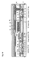
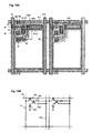
- Figs. 1 to 2B are used in explaining the preferred embodiments of the present invention. Shown in Fig. 1 is a cross sectional diagram of a pixel of an EL display device of the present invention, in Fig. 2A is its top view, and in Fig. 2B is a circuit composition. In practice, a pixel portion (image display portion) is formed with a multiple number of this type of pixel arranged in a matrix state.
- FIG. 1 shows a cross section cut along the line A-A' in the top view shown in Fig. 2A.
- Common symbols are used in Fig. 1 and in Figs. 2A and 2B, and therefore the three figures may be referenced as appropriate.
- two pixels are shown in the top view of Fig. 2A, and both have the same structure.
- Reference numeral 11 denotes a substrate
- reference numeral 12 denotes a base film in Fig. 1.
- a glass substrate, a glass ceramic substrate, a quartz substrate, a silicon substrate, a ceramic substrate, a metallic substrate, or a plastic substrate (including a plastic film) can be used as the substrate 11.
- the base film 12 is especially effective for cases in which a substrate containing mobile ions, or a substrate having conductivity, is used, but need not be formed for a quartz substrate.
- An insulating film containing si I icon may be formed as the base film 12.
- the term "insulating film containing silicon” indicates, specifically, an insulating film that contains silicon, oxygen, and nitrogen in predetermined ratios such as a silicon oxide film, a silicon nitride film, or a silicon oxynitride film (denoted by SiO x N y ).
- Reference numeral 201 denotes a TFT functioning as a switching element (hereafter referred to as a switching TFT), and reference numeral 202 denotes a TFT functioning as a current control element for controlling the amount of current flowing to an EL element (hereafter referred to as a current control TFT), and both are formed by an n-channel TFT.
- switching TFT switching element
- current control TFT current control TFT
- the field effect mobility of the n-channel TFT is larger than the field effect mobility of a p-channel TFT, and therefore the operation speed is fast and electric current can flow easily. Further, even with the same amount of current flow, the n-channel TFT can be made smaller. The effective surface area of the display portion therefore becomes larger when using the n-channel TFT as a current control TFT, and this is preferable.
- the p-channel TFT has the advantages that hot carrier injection essentially does not become a problem, and that the off current value is low, and there are already reports of examples of using the p-channel TFT as a switching TFT and as a current control TFT.
- the present invention is characterized by the use of n-channel TFTs for all of the TFTs within all of the pixels.
- the switching TFT 201 is formed having: an active layer comprising a source region 13, a drain region 14, LDD regions 15a to 15d, a high concentration impurity region 16, and channel forming regions 17a and 17b; a gate insulating film 18; gate electrodes 19a and 19b, a first interlayer insulating film 20, a source wiring 21, and a drain wiring 22.
- the present invention is characterized in that the gate electrodes 19a and 19b become a double gate structure electrical ly connected by a gate wiring 211 which is formed by a different material (a material having a lower resistance than the gate electrodes 19a and 19b).
- a different material a material having a lower resistance than the gate electrodes 19a and 19b.
- a so-called multi-gate structure a structure containing an active layer having two or more channel forming regions connected in series
- the multi-gate structure is extremely effective in lowering the value of the off current, and by making the switching TFT 201 of the pixel into a multi-gate structure with the present invention, a low off current value can be real ized for the switching TFT.
- the active layer is formed by a semiconductor film containing a crystal structure.
- a single crystal semiconductor film may be used, and a polycrystalline semiconductor film or a microcrystalline semiconductor film may also be used.
- the gate insulating film 18 may be formed by an insulating film containing silicon. Additionally, a conducting film can be used for all of the gate electrodes, the source wiring, and the drain wiring.
- the LDD regions 15a to 15d in the switching TFT 201 are formed so as not to overlay with the gate electrodes 19a and 19b by interposing the gate insulating film 18. This structure is extremely effective in reducing the off current value.
- an offset region (a region that comprises a semiconductor layer having the same composition as the channel forming regions, and to which a gate voltage is not applied) between the channel forming regions and the LDD regions is more preferable for reducing the off current value.
- the high concentration impurity region formed between the channel forming regions is effective in lowering the value of the off current.
- the multi-gate structure TFT as the switching TFT 201, as above, a switching element having a sufficiently low off current value is realized by the present invention.
- the gate voltage of the current control element can therefore be maintained for a sufficient amount of time (for a period from one selection until the next selection) without forming a capacitor (Cs), such as the one stated in the conventional example.
- the current control TFT 202 is formed having: an active layer comprising a source region 31, a drain region 32, an LDD region 33, and a channel forming region 34; a gate insulating film 18; a gate electrode 35; the first interlayer insulating film 20; a source wiring 36; and a drain wiring 37.
- the gate electrode 35 has a single gate structure, but a multi-gate structure may also be used.
- the drain of the switching TFT 201 is electrically connected to the gate of the current control TFT 202.
- the gate electrode 35 of the current control TFT 202 is electrically connected to the drain region 14 of the switching TFT 201 through the drain wiring (also referred to as a connection wiring) 22.
- the source wiring 36 is connected to an electric current supply wiring 212.
- a characteristic of the current control TFT 202 is that its channel width is larger than the channel width of the switching TFT 201. Namely, as shown in Fig. 8, when the channel length of the switching TFT is taken as L1 and its channel width as W1, and the channel length of the current control TFT is taken as L2 and its channel width as W2, a relational expression is reached in which W2 / L2 ⁇ 5 ⁇ W1 / L1 (preferably W2 / L2 ⁇ 10 ⁇ W1 / L1). Consequently, it is possible for more current to easily flow in the current control TFT than in the switching TFT.
- the channel length L1 of the multi-gate structure switching TFT is the sum of each of the channel lengths of the two or more channel forming regions formed.
- a double gate structure is formed in the case of Fig. 8, and therefore the sum of the channel lengths L1a and L1b, respectively, of the two channel-forming regions becomes the channel length L1 of the switching TFT.
- the channel lengths L1 and L2, and the channel widths W1 and W2 are not specifically limited to a range of values with the present invention, but it is preferable that W1 be from 0.1 to 5 ⁇ m (typically between 1 and 3 ⁇ m), and that W2 be from 0.5 to 30 ⁇ m (typically between 2 and 10 ⁇ m). It is preferable that L1 be from 0.2 to 18 ⁇ m (typically between 2 and 15 ⁇ m), and that L2 be from 0.1 to 50 ⁇ m (typically between 1 and 20 ⁇ m) at this time.
- the channel length L in the current control TFT is set on the long side in order to prevent excessive current flow.
- W2 / L2 ⁇ 3 (more preferably W2 / L2 ⁇ 5).
- the current flow per pixel is from 0.5 to 2 ⁇ A (better between 1 and 1.5 ⁇ A).
- the length (width) of the LDD region formed in the switching TFT 201 is set from 0.5 to 3.5 ⁇ m, typically between 2.0 and 2.5 ⁇ m.
- the EL display device shown in Fig. 1 is characterized in that the LDD region 33 is formed between the drain region 32 and the channel forming region 34 in the current control TFT 202.
- the LDD region 33 has both a region which overlaps, and a region which does not overlap the gate electrode 35 by interposing a gate insulating film 18.
- the current control TFT 202 supplies a current for making the EL element 203 luminesce, and at the same time controls the amount supplied and makes gray scale display possible. It is therefore necessary that there is no deterioration when the current flows, and that steps are taken against deterioration due to hot carrier injection. Furthermore, when black is displayed, the current control TFT 202 is set in the off state, but if the off current value is high, then a clean black color display becomes impossible, and this invi tes problems such as a reduction in contrast. It is therefore necessary to suppress the value of the off current.
- the length of the LDD region which overlaps the gate electrode may be made from 0. 1 to 3 ⁇ m (preferable between 0.3 and 1.5 ⁇ m) at this point. If it is too long, then the parasitic capacitance will become larger, and if it is too short, then the effect of preventing hot carrier will become weakened. Further, the length of the LDD region not overlapping the gate electrode may be set from 1. 0 to 3.5 ⁇ m (preferable between 1.5 and 2.0 ⁇ m). If it is too long, then a sufficient current becomes unable to flow, and if it is too short, then the effect of reducing off current value becomes weakened.
- a parasitic capacitance is formed in the above structure in the region where the gate electrode and the LDD region overlap, and therefore it is preferable that this region not be formed between the source region 31 and the channel forming region 34.
- the carrier (electrons in this case) flow di rection is always the same for the current control TFT, and therefore it is sufficient to form the LDD region on only the drain region side.
- the film thickness of the active layer (especially the channel forming region) of the current control TFT 202 thick (preferably from 50 to 100 nm, more preferably between 60 and 80 nm).
- the film thickness of the active layer (especially the channel forming region) thin (preferably from 20 to 50 nm, more preferably between 25 and 40 nm).
- the above chemical compounds can also be combined with another element.
- nitrated aluminum oxide denoted by AlN x 0 y
- nitrogen is added to aluminum oxide.
- This material also not only possesses heat radiation qualities, but also is effective in preventing the penetration of substances such as moisture and alkaline metals.
- x and y are arbitrary integers for the above nitrated aluminum oxide.
- Reference numeral 42 denotes a color filter
- reference numeral 43 denotes a fluorescent substance (also referred to as a fluorescent pigment layer). Both are a combination of the same color, and contain red (R), green (G), or blue (B).
- the color filter 42 is formed in order to increase the color purity
- the fluorescent substance 43 is formed in order to perform color transformation.
- a second interlayer insulating film 44 is formed by a second interlayer insulating film 44.
- a resin film is preferable as the second interlayer insulating film 44, and one such as polyimide, polyamide, acrylic, or BCB (benzocyclobutane) may be used.
- An inorganic film may, of course, also be used, provided that sufficient level ing is possible.
- the leveling of steps due to the TFT by the second interlayer insulating film 44 is extremely important.
- the EL layer formed afterward is very thin, and therefore there are cases in which poor luminescence is caused by the existence of a step. It is therefore preferable to perform leveling before forming a pixel electrode so as to be able to form the EL layer on as level a surface as possible.
- thermal radiation layer an insulating film having a high thermal radiation effect (hereafter referred to as a thermal radiation layer) on the second interlayer insulating film 44.
- This type of thermal radiation layer functions so that the heat generated by the EL element is released, so that heat is not stored in the EL element.
- the second interlayer insulating film 44 is weak with respect to heat, and the thermal radiation layer works so as not to impart bad influence due to the heat generated by the EL element.
- the thermal radiation layer can also function as a protecting layer in order that alkaline metals within the EL layer do not diffuse toward the TFT, at the same time as preventing deterioration of the EL element and the resin film due to heat, as above.
- the thermal radiation layer also functions as a protecting layer so that moisture and oxygen do not penetrate into the EL layer from the TFT.
- a carbon film such as a diamond film or a diamond-like carbon film is preferable, and in order to prevent penetration of substances such as moisture, it is more preferable to use a lamination structure of a carbon film and a silicon nitride film (or a silicon oxynitride film).
- Reference numeral 45 denotes a pixel electrode (EL element anode) made from a transparent conducting film. After opening a contact hole in the second interlayer insulating film 44 and in the first passivation film 41, the pixel electrode 45 is formed so as to be connected to the drain wiring 37 of the current control TFT 202.
- Q is either N or a C-R (carbon chain);
- M is a metal, a metal oxide, or a metal hal ide;
- R is hydrogen, an alkyl, an aralkyl, an aryl, or an alkalyl; and
- T1 and T2 are unsaturated six member rings including substituent such as hydrogen, alkyl, or halogen.
- R 2 through R 7 are defined as stated above; L 1 through L 5 are carbohydrate groups containing from 1 to 12 carbon elements; and both L 1 and L 2' or both L 2 and L 3 are formed by benzo-rings. Further, a metal oxinoid such as the following may also be used.
- a material containing a low work coefficient material such as magnesium (Mg), lithium (Li), cesium (Cs), barium (Ba), potassium (K), beryllium (Be), or calcium (Ca) is used as the cathode 47.
- a MgAgAl electrode, a LiAl electrode, and a LiFAI electrode can be given as other examples.
- the protecting electrode 48 is an electrode formed in order to be a protecting film against moisture from external to the cathode 47, and a material containing aluminum (AI) or silver (Ag) is used.
- the protecting electrode 48 also has a heat radiation effect.
- the EL layer is extremely weak with respect to heat, and therefore it is preferable to use vacuum evaporation (in particular, an organic molecular beam evaporation method is effective in that it forms a very thin film, on the molecular order level), sputtering, plasma CVD, spin coating, screen printing, or ion plating as the film deposition method. It is also possible to form the EL layer by an ink-jet method.
- the ink jet method there is a bubble jet method using cavitation (refer to Japanese Patent Application Laid-open No. Hei 5-116297), and there is a piezo method using a piezo element (refer to Japanese Patent Application Laid-open No. Hei 8-290647), and in view of the fact that organic EL materials are weak with respect to heat, the piezo method is preferable.
- the EL layer is weak with respect to heat, as stated above, and therefore it is preferable to perform film deposition at a low temperature as possible (preferably in the range from room temperature to 120°C). It can therefore be said that plasma CVD, sputtering, vacuum evaporation, ion plating, and solution application (spin coating) are desirable film deposition methods.
- the EL display device of the present invention has a pixel portion containing a pixel with a structure as stated above, and TFTs having differing structures in response to their function are arranged in the pixel.
- a switching TFT having a sufficiently low off current value, and a current control TFT which is strong with respect to hot carrier injection can be formed within the same pixel, and an EL display device having high reliability and which is capable of good image display can thus be formed.
- CMOS circuit is shown as a basic circuit for the driver circuits.
- a base film 301 is formed wi th a 300 nm thickness on a glass substrate 300.
- Silicon oxynitride films are laminated as the base film 301 in embodiment 1. It is good to set the nitrogen concentration to between 10 and 25 wt% in the film contacting the glass substrate 300.
- a heat radiating layer made from the same material as that of the first passivation film 41 shown in Fig. 1, as a portion of the base film 301.
- a large electric current flows in a current control TFT heat is easily generated, and therefore it is effective to form the heat radiating layer as close as possible to the current control TFT.
- an amorphous silicon film (not shown in the figures) is formed with a thickness of 50 nm on the base film 301 by a known deposition method. Note that it is not necessary to limit this to the amorphous silicon film, and another film may be formed provided that it is a semiconductor film containing an amorphous structure (including a microcrystalline semiconductor film). In addition, a compound semiconductor film containing an amorphous structure, such as an amorphous silicon germanium film, may also be used. Further, the film thickness may be made from 20 to 100 nm.
- the amorphous silicon film is then crystallized by a known method, forming a crystalline silicon film (also referred to as a polycrystalline silicon film or a polysilicon film) 302.
- a crystalline silicon film also referred to as a polycrystalline silicon film or a polysilicon film
- Thermal crystallization using an electric furnace, laser annealing crystallization using a laser, and lamp annealing crystallization using an infrared lamp exist as known crystallization methods. Crystallization is performed in embodiment 1 using light from an excimer laser which uses XeCl gas.
- pulse emission type excimer laser light formed into a linear shape is used in embodiment 1, but a rectangular shape may also be used, and continuous emission argon laser light and continuous emission excimer laser light can also be used.
- the crystalline silicon film is used as an active layer of the TFTs in embodiment 1, but it is also possible to use an amorphous silicon film as the active layer. However, it is necessary for a large current to flow through the current control TFT, and therefore it is more effective to use the crystalline silicon film, through which current easily flows.
- a protecting film 303 is formed on the crystalline silicon film 302 from a silicon oxide film having a thickness of 130 nm. This thickness may be chosen within the range of 100 to 200 nm (preferably between 130 and 170 nm). Furthermore, other films may also be used providing that they are insulating films containing silicon.
- the protecting film 303 is formed so that the crystalline silicon film is not directly exposed to plasma during addition of an impurity, and so that it is possible to have delicate concentration control of the impurity.
- Resist masks 304a and 304b are then formed on the protecting film 303, and an impurity element which imparts n-type conductivity (hereafter referred to as an n-type impurity element) is added.
- an impurity element which imparts n-type conductivity hereafter referred to as an n-type impurity element
- elements residing in periodic table group 15 are generally used as the n-type impurity element, and typically phosphorous or arsenic can be used.
- a plasma doping method is used, in which phosphine (PH 3 ) is plasma activated without separation of mass, and phosphorous is added at a concentration of 1x10 18 atoms/cm 3 in embodiment 1.
- An ion implantation method, in which separation of mass is performed, may also be used, of course.
- the dose amount is regulated so that the n-type impurity element is contained in n-type impurity regions 305 and 306, thus formed by this process, at a concentration of 2x10 16 to 5x10 19 atoms/cm 3 (typically between 5x10 17 and 5x10 18 atoms/cm 3 ).
- the protecting film 303 is removed, and activation of the added periodic table group 15 element is performed.
- a known technique of activation may be used as the means of activation, and activation is done in embodiment 1 by irradiation of excimer laser light. Both of pulse emission type laser and a continuous emission type laser may be used, and it is not necessary to place any limits on the use of excimer laser light.
- the goal is the activation of the added impurity element, and it is preferable that irradiation is performed at an energy level at which the crystalline silicon film does not melt. Note that the laser irradiation may also be performed with the protecting film 303 in place.
- Activation by heat treatment may also be performed along with activation of the impurity element by laser light.
- activation is performed by heat treatment, considering the heat resistance of the substrate, it is good to perform heat treatment on the order of 450 to 550°C.
- a boundary portion (connecting portion) with regions along the edges of the n-type impurity regions 305 and 306, namely regions along the perimeter into which the n-type impurity element, which exists in the n-type impurity regions 305 and 306, is not added, is delineated by this process. This means that, at the point when the TFTs are later completed, extremely good connections can be formed between LDD regions and channel forming regions.
- a gate insulating film 311 is formed, covering the active layers 307 to 310.
- a single layer structure or a lamination structure may be used.
- a 110 nm thick silicon oxynitride film is used in embodiment 1.
- the gate wirings may be formed by a single layer conducting film, and when necessary, it is preferable to use a two layer or a three layer lamination film. All known conducting films can be used as the gate electrode material. However, as stated above, it is preferable to use a material which is capable of being micro-processed, specifically, a material which is capable of being patterned to a line width of 2 ⁇ m or less.
- a single layer film or a lamination may be used, of course.
- a lamination film made from a 50 nm thick tantalum ni tride (TaN) film and a 350 nm thick Ta film is used in embodiment 1. It is good to form this film by sputtering. Furthermore, if an inert gas such as Xe or Ne is added as a sputtering gas, then film peeling due to the stress can be prevented.
- TaN tantalum ni tride
- the gate electrodes 313 and 316 are formed at this time so as to overlap a portion of the n-type impurity regions 305 and 306, respectively, sandwiching the gate insulating film 311. This overlapping portion later becomes an LDD region overlapping the gate electrode.
- Resist masks 324a to 324d are formed next to cover the gate electrodes, as shown in Fig. 4B, and an n-type impurity element (phosphorous is used in embodiment 1) is added, forming impurity regions 325 to 331 containing a high concentration of phosphorous. Ion doping using phosphine (PH 3 ) is also performed here, and is regulated so that the phosphorous concentration of these regions is from 1x10 20 to 1x10 21 atoms/cm 3 (typically between 2x10 20 and 5x10 20 a toms/cm 3 ).
- a source region or a drain region of the n-channel TFT is formed by this process, and in the switching TFT, a portion of the n-type impurity regions 320 to 322 formed by the process of Fig. 4A remains. These remaining regions correspond to the LDD regions 15a to 15d of the switching TFT in Fig. 1.
- phosphorous has already been added to the impurity regions 333 and 334 at a concentration of 1x10 16 to 5x10 18 atoms/cm 3 , but boron is added here at a concentration of at least 3 times that of the phosphorous. Therefore, the n-type impurity regions already formed completely invert top-type, and function as p-type impurity regions.
- a gate wiring 335 with a thickness of 300 nm is formed next.
- a metallic film having aluminum (Al) or copper (Cu) as its principal constituent (comprising 50 to 100% of the composition) may be used as the material of the gate wiring 335.
- the gate wiring 335 is formed with a placement so that the gate electrodes 314 and 315 of the switching TFTs (corresponding to gate electrodes 19a and 19b of Fig. 2) are electrically connected. (See Fig. 4D.)
- the wiring resistance of the gate wiring can be made extremely small by using this type of structure, and therefore a pixel display region (pixel portion) having a large surface area can be formed.
- the pixel structure of embodiment 1 is extremely effective because an EL display device having a screen size of a 10 inch diagonal or larger (in addition, a 30 inch or larger diagonal) is realized.
- a first interlayer insulating film 336 is formed next, as shown in Fig. 5A.
- a single layer insulating film containing silicon is used as the first interlayer insulating film 336, but a lamination film may be combined in between. Further, a film thickness of between 400 nm and 1.5 ⁇ m may be used.
- a lamination structure of an 800 nm thick silicon oxide film on a 200 nm thick silicon oxynitride film is used in embodiment 1.
- the hydrogenation step may also be inserted during the formation of the first interlayer insulating film 336. Namely, hydrogen processing may be performed as above after forming the 200 nm thick silicon oxynitride film, and then the remaining 800 nm thick silicon oxide film may be formed.
- the respective film thickness may be chosen in the range of 0. 5 to 5 ⁇ m (typically between 1 and 2 ⁇ m).
- the optimal film thickness of the fluorescing body 346 varies with the material used. In other words, if it is too thin, then the color transformation efficiency becomes poor, and if it is too thick, then the step becomes large and the amount of light transmitted drops. Optimal film thicknesses must therefore be set by taking a balance of both characteristics.
- a second interlayer insulating film 347 is formed next from an organic resin.
- Materials such as polyimide, polyamide, acryl ic, and BCB (benzocyclobutene) can be used as the organic resin.
- the purpose of being a leveling film is strong in the second interlayer insulating film 347, and therefore acrylic, having superior leveling characteristics, is preferable.
- An acrylic film is formed in embodiment 1 with a film thickness which can sufficiently level the step between the color filter 345 and the fluorescing body 346. This thickness is preferably from 1 to 5 ⁇ m (more preferably between 2 and 4 ⁇ m).
- embodiment 1 becomes a structure in which the pixel electrode 348 is electrically connected to the drain region 331 of the current control TFT, through the drain wi ring 343. This structure has the following advantages.
- the pixel electrode 348 becomes directly connected to an organic material such as the EL layer (emitting layer) or a charge transporting layer, and therefore it is possible for the mobile ions contained in the EL layer to diffuse throughout the pixel electrode. In other words, without connecting the pixel electrode 348 directly to the drain region 331, a portion of the active layer, the introduction of mobile ions into the active layer due to the drain wiring 343 being interrupted can be prevented in the structure of embodiment 1.
- an EL layer 349, a cathode (MgAg electrode) 350, and a protecting electrode 351 are formed in succession without exposure to the atmosphere. It is preferable, at this point, to perform heat treatment of the pixel electrode 348, completely removing all moisture, before forming the EL layer 349 and the cathode 350. Note that a known material can be used as the EL layer 349.
- the materials explained in the "embodiment mode" section of this specification can be used as the EL layer 349.
- an EL layer having a 4 layer structure of a hole injecting layer, a hole transporting layer, an emitting layer, and an electron transporting layer is used, as shown in Fig. 19, but there are cases in which the electron transporting layer is not formed, and cases in which an electron injecting layer is also formed. Furthermore, there are also cases in which the hole injecting layer is omitted.
- these types of combinations have already been reported, and any of these constitutions may be used.
- An amine such as TPD may be used as the hole injecting layer or as the hole transporting layer, and in addition, a hydrazone (typically DEH), a stilbene(typically STB), or a starburst (typically m-MTDATA) can also be used.
- a starburst material which has a high glass transition temperature and is difficult to crystallize, is preferable.
- polyaniline (PAni), polythiophene (PEDOT), and copper phthalocyanine (CuPc) may also be used.
- BPPC, perylene, and DCM can be used as a red color emitting layer in the emitting layer, and in particular, the Eu complex shown by Eu(DBM) 3 (Phen) (refer to Kido, J., et. al, Appl. Phys., vol. 35, pp. L394-6, 1996 for details) is highly monochromatic, possessing a sharp emission at a wavelength of 620 nm.
- a 300 nm thick silicon nitride film is formed as a second passivation film 352, and this may also be formed in succession, without exposure to the atmosphere, after formation of the protecting electrode 351.
- the same materials as those of the second passivation film 49 of Fig. 1 can also be used, of course, as the second passivation film 352.
- a 4 layer structure made from a hole injecting layer, a hole transporting layer, an emitting layer, and an electron injecting layer is used in embodiment 1, but there are already examples of many combinations already reported, and any of these constitutions may also be used.
- an MgAg electrode is used as the cathode of the EL element in embodiment 1, but other known materials may also be used.
- the protecting electrode 351 is formed in order to prevent deterioration of the MgAg electrode 350, and a metallic film having aluminum as its principal constituent is typical. Other materials may, of course, also be used. Furthermore, the EL layer 349 and the MgAg electrode 350 are extremely weak with respect to moisture, and therefore it is preferable to perform successive formation up through to the protecting electrode 351 without exposure to the atmosphere, protecting the EL layer from external air.
- the film thickness of the EL layer 349 may be from 10 to 400 nm (typically between 60 and 160 nm), and that the thickness of the MgAg electrode 350 may be from 180 to 300 nm (typically between 200 and 250 nm).
- a TFT having a structure which reduces hot carrier injection as much as possible without a drop in the operation speed is used as an n-channel TFT 205 of the CMOS circuit forming the driver circuits.
- the driver circuits referred to here include circuits such as a shift register, a buffer, a level shifter, and a sampling circuit (also referred to as a transfer gate).
- signal conversion circuits such as a D/A converter circuit are also included.
- an active layer of the n-channel TFT 205 includes a source region 355, a drain region 356, an LDD region 357, and a channel forming region 358, as shown in Fig. 5C, and the LDD region 357 overlaps the gate electrode 313, sandwiching the gate insulating film 311.
- the formation of the LDD region on the drain side only is in consideration of not lowering the operation speed. Further, it is not necessary to be concerned with the value of the off current in the n-channel TFT 205, and greater emphasis may be placed on the operation speed. It is therefore preferable that the LDD region 357 completely overlap the gate electrode 313, reducing resistive components as much as possible. In other words, it is good to eliminate all offset.
- Deterioration of a p-channel TFT 206 of the CMOS circuit due to hot carrier injection is almost of no concern, and in particular, therefore, an LDD region is not formed. It is also possible, of course, to take action against hot carriers by forming an LDD region similar to that of the n-channel TFT 205.
- the sampling circuit is somewhat special when compared to the other circuits, and a large current flows in the channel forming region in both directions. Namely, the roles of the source region and the drain region change. In addition, it is necessary to suppress the value of the off current as much as possible, and with that in mind, it is preferable to arrange a TFT having functions at an intermediate level between the switching TFT and the current control TFT.
- a TFT with the structure shown in Fig. 9 is an n-type TFT forming the sampling circuit.
- This effect is as stated in the explanation of the current control TFT 202, and the case of the sampling circuit differs in the point of forming the LDD regions 901a and 901b with a shape that sandwiches a channel forming region 904.
- a pixel with the structure shown in Fig. 1 is formed, forming a pixel portion.
- the structures of a switching TFT and a current control TFT formed within the pixel have already been explained in Fig. 1, and therefore that explanation is omitted here.
- a housing material such as a highly airtight protecting film (such as a laminar film or an ultraviolet hardened resin film) or a ceramic sealing can, so that there is no exposure to the atmosphere.
- a housing material such as a highly airtight protecting film (such as a laminar film or an ultraviolet hardened resin film) or a ceramic sealing can, so that there is no exposure to the atmosphere.
- a connector (a flexible printed circuit, FPC) for connecting between output terminals from elements or circuits formed on the substrate, and external signal terminals, is attached, completing a manufactured product.
- FPC flexible printed circuit
- the source of the current control TFT 608 is connected to a current supply line 609, and an EL element 610 is electrically connected to the drain of the current control TFT 608.
- the current control TFT 608 is an n-channel TFT, it is preferable to connect the cathode of the EL element 610 to the drain of the current control TFT 608 at this point.
- the current control TFT 608 is a p-channel TFT, then it is preferable to connect the anode of the EL element 610 to the drain of the current control TFT 608.
- Input wirings (connection wirings) 612 and 613, and an input wiring 614 which is connected to the current supply line 609, are then formed in an external input terminal FPC 611 in order to transfer signals to the driver circuits.
- Fig. 7 Shown in Fig. 7 is one example of the circuit composition of the EL display device shown in Fig. 6.
- the EL display device of embodiment 1 has a source side driving circuit 701, a gate side driving circuit (A) 707, a gate side driving circuit (B) 711, and a pixel portion 706.
- driver circuit is a generic term which includes source side processing circuits and gate side processing circuits.
- the source side driving circuit 701 is provided with a shift register 702, a level shifter 703, a buffer 704, and a sampling circuit (transfer gate) 705.
- the gate side driving circuit (A) 707 is provided with a shift register 708, a level shifter 709, and a buffer 710.
- the gate side driving circuit (B) 711 has a similar composition.
- the driving voltage is from 5 to 16 V (typically 10 V) for the shifter registers 702 and 708 here, and the structure shown by reference numeral 205 of Fig. 5C is suitable for an n-channel TFT used in a CMOS circuit forming the circuits.
- CMOS circuit containing the n-channel TFT 205 of Fig. 5C is suitable.
- a multi-gate structure such as a double gate structure or a triple gate structure for the gate wirings, is effective by increasing the reliability of each circuit.
- the driving voltage is between 14 and 16 V for the sampling circuit 705, but it is necessary to reduce the value of the off current because the source region and the drain region invert, and therefore a CMOS circuit containing the n-channel TFT 208 of Fig. 9 is suitable.
- a pixel portion 1701, a source side driving circuit 1702, and a gate side driving circuit 1703 are formed on a substrate (including a base film underneath a TFT) 1700.
- Various wirings from the respective driver circuits are connected to external equipment, via the FPC 611, through the input wirings 612 to 614.
- an insulating substance such as a glass or a polymer as the housing material 1704.
- amorphous glass such as borosilicate glass or quartz
- crystallized glass such as borosilicate glass or quartz
- ceramic glass organic resins (such as acrylic resins, styrene resins, polycarbonate resins, and epoxy resins); and silicone resins.
- ceramics may also be used.
- the adhesive 1705 is an insulating material, it is also possible to use a metallic material such as a stainless alloy.
- an adhesive such as an epoxy resin or an acrylate resin as the material of the adhesive 1705.
- a thermally hardened resin or a light hardened resin can also be used as the adhesive. Note that it is necessary to use a material through which, as much as is possible, oxygen and moisture is not transmitted.
- an opening 1706 between the housing material and the substrate 1700 is preferable to fill an opening 1706 between the housing material and the substrate 1700 with an inert gas (such as argon, helium, or nitrogen).
- an inert gas such as argon, helium, or nitrogen.
- an inert liquid such as a liquid fluorinated carbon, typically perfluoroalkane.
- the materials such as those used by Japanese Patent Application Laid-open No. Hei 8-78519 may be referred to regarding inert liquids.
- the space may also be filled with a resin.
- drying agent in the opening 1706.
- Materials such as those recorded in Japanese Patent Application Laid-open No. Hei 9-148066 can be used as the drying agent.
- barium oxide may be used.
- it is effective to form an antioxidizing agent as well, not just a drying agent.
- a plural number of isolated pixels having EL elements are formed in the pixel portion, as shown in Fig. 17B, and all of the pixels have a protecting electrode 1707 as a common electrode.
- the EL layer, the cathode (MgAg electrode), and the protecting electrode in succession, wi thout exposure to the atmosphere.
- the EL layer and the cathode are formed using the same mask material, and provided that only the protecting electrode is formed by a separate mask material, then the structure of Fig. 17B can be realized.
- the EL layer and the cathode may be formed only in the pixel portion at this point, and it is not necessary to form them on the driving circuits. There is no problem, of course, with forming them on the driving circuits, but considering the fact that alkaline metals are contained in the EL layer, it is preferable to not form it over the driving circuits.
- an input wiring 1709 is connected to the protecting electrode 1707 in a region shown by reference numeral 1708.
- the input wiring 1709 is a wiring for providing a preset voltage to the protecting electrode 1707, and is connected to the FPC 611 through a conducting paste material (typically an anisotropic conducting film) 1710.
- FIG. 18A to 18C A manufacturing process for realizing a contact structure in the region 1708 is explained here using Figs. 18A to 18C.
- Fig. 5A the state of Fig. 5A is obtained in accordance with the processes of embodiment 1.
- the first interlayer insulating film 336 and the gate insulating film 311 are removed from the edges of the substrate (in the region shown by reference numeral 1708 in Fig. 17B), and the input wiring 1709 is formed on that region.
- the source wirings and the drain wirings of Fig. 5A are of course formed at the same time. (See Fig. 18A.)
- the current supply line 64 can be made common between neighboring pixels, as in embodiment 2, and that a structure like that of embodiment 3 may also be used. Furthermore, processes of manufacturing may be performed in accordance with those of embodiment 1.
- the current control TFT 1302 comprises: a gate electrode 82; the gate insulating film 72; a source region 83; a drain region 84; an LDD region 85; a channel forming region 86; a channel protecting film 87; a first interlayer insulating film 79; a source wiring 88; andadrainwiring89.
- the gate electrode 82 is electrically connected to the drain wiring 81 of the switching TFT 1301 at this point.
- the above switching TFT 1301 and the current control TFT 1302 may be formed in accordance with a known method of manufacturing a reverse stagger type TFT. Further, similar materials used in corresponding portions of the top gate type TFTs of embodiment 1 can be used for the materials of each portion (such as wirings, insulating films, and active layers) formed in the above TFTs. Note that the channel protecting films 78a, 78b, and 87, which are not in the constitution of the top gate type TFT, may be formed by an insulating film containing silicon. Furthermore, regarding the formation of impurity regions such as the source regions, the drain regions, and the LDD regions, they may be formed by using a photolithography technique and individually changing the impurity concentration.
- Embodiment 1 may be referred to with respect to manufacturing processes and materials for the above.
- the effect of protecting from the diffusion of mobile ions from the substrate is also very important, of course, and therefore it is preferable to use a lamination structure of a compound including Si, Al, N, 0, and M, and an insulating film containing silicon, similar to the first passivation film 41.
- the light emitted from the EL layer is radiated in the direction opposite to the substrate, and therefore it is not necessary to pay attention to the transmissivity of materials, such as the insulating film, which exist between the substrate and the pixel electrode. In other words, materials which have a somewhat low transmissivity can also be used.
- a carbon film such as one referred to as a diamond thin film, a diamond-like carbon film, or an amorphous carbon film, as the base film 12 or the first passivation film 41.
- the film thickness can be set thick, to between 100 and 500 nm, and it is possible to have a very high thermal radiating effect.
- the film thickness is set to between 5 and 100 nm.
- embodiment 7 is effective when the pixel structure shown in embodiment 3 is used, and for other constitutions, it is possible to freely combine the constitution of embodiment 7 with the constitution of any of embodiments 1 to 6.
- the amount of the off current value in the switching TFT in the pixel of the EL display device is reduced by using a multi-gate structure for the switching TFT, and the present invention is characterized by the elimination of the need for a storage capacitor.
- This is a device for making good use of the surface area, reserved for the storage capacitor, as an emitting region.
- the object of the present invention can be sufficiently achieved by reducing the value of the off current by using a multi-gate structure for the switching TFT, and by only shrinking the exclusive surface area of the storage capacitor.
- the different point between Fig. 14 and Fig. 1 is the existence of a storage capacitor 1401 connected to the switching TFT.
- the storage capacitor 1401 is formed by a semiconductor region (lower electrode) extended from the drain region 14 of the switching TFT 201, the gate insulating film 18, and a capacitor electrode (upper electrode) 1403.
- the capacitor electrode 1403 is formed at the same time as the gate electrodes 19a, 19b, and 35 of the TFT.
- Laser crystallization is used as the means of forming the crystalline silicon film 302 in embodiment 1, and a case of using a different means of crystallization is explained in embodiment 9.
- crystallization is performed using the technique recorded in Japanese Patent Application Laid-open No. Hei 7-130652.
- the technique recorded in the above patent application is one of obtaining a crystalline silicon film having good crystallinity by using an element such as nickel as a catalyst for promoting crystallization.
- a TFT may be formed using the technique recorded in the specification of Japanese Patent Application Laid-open No. Hei 11-076967 by the applicant of the present invention.
- the analog signal When analog driving is performed, the analog signal is sent to a source wiring of a switching TFT, and the analog signal, which contains gray scale information, becomes the gate voltage of a current control TFT.
- the current flowing in an EL element is then controlled by the current control TFT, the EL element emitting intensity is controlled, and gray scale display is performed.
- V ds is the voltage difference between a source region and a drain region
- V gs is the voltage difference between the source region and a gate electrode
- V th is the threshold voltage of the TFT.
- the EL element has an extremely fast response speed in comparison to a liquid crystal element, and therefore it is possible to have high speed driving. Therefore, the EL element is one which is suitable for time ratio gray scale driving, in which one frame is partitioned into a plural number of subframes and then gray scale display is performed. Furthermore, it has the advantage of the period of one frame being short, and therefore the amount of time for which the gate voltage of the current control TFT is maintained is also short, and a storage capacitor can be made smaller or eliminated.
- the present invention is a technique related to the element structure, and therefore any method of driving it may thus be used.
- Figs. 21A and 21B examples of the pixel structure of the EL display device of the present invention are shown in Figs. 21A and 21B.
- reference numeral 4701 denotes a source wiring of a switching TFT 4702.
- reference numeral 4703 denotes a gate wiringof the switching TFT 4702
- reference numeral 4704 denotes a current control TFT
- 4705 denotes an electric current supply line
- 4706 denotes a power source control TFT
- 4707 denotes a power source control gate wiring
- 4708 denotes an EL element.
- Japanese Patent Application Laid-open No. Hei 11-341272 may be referred to regarding the operation of the power source control TFT 4706.
- Fig. 21B is an example of a case in which an electric current supply line 4710 is formed parallel to the gate wiring 4703, and in which a power source control gate wiring 4711 is formed parallel to the source wiring 4701.
- the structure is formed such that the electric current supply line 4710 and the gate wiring 4703 do not overlap, but provided that both are wirings formed on different layers, then they can be formed to overlap, sandwiching an insulating film.
- the exclusive surface area of the electric current supply line 4710 and the gate wiring 4703 can be shared, and the pixel section can be made even more high precision.
- Figs. 22A and 22B examples of the pixel structure of the EL display device of the present invention are shown in Figs. 22A and 22B.
- reference numeral 4801 denotes a source wiring of a switching TFT 4802
- reference numeral 4803 denotes a gate wiring of the switching TFT 4802
- reference numeral 4804 denotes a current control TFT
- 4805 denotes an electric current supply line
- 4806 denotes an erasure TFT
- 4807 denotes an erasure gate wiring
- 4808 denotes an EL element.
- Japanese Patent Application Laid-open No. Hei 11-338786 may be referred to regarding the operation of the erasure TFT 4806.
- the EL display device of the present invention may have a structure in which several TFTs are formed within a pixel. In embodiments 11 and 12, examples of forming three TFTs are shown, but from 4 to 6 TFTs may also be formed. It is possible to implement the present invention without placing any limitations on the structure of the pixels of the EL display device.
- Embodiment 1 may be referred to for a method of manufacturing the p-channel TFT used in embodiment 14.
- An active layer of the p-channel TFT comprises a source region 2801, a drain region 2802, and a channel forming region 2803, and the source region 2801 is connected to the source wiring 36, and the drain region 2802 is connected to the drain wiring 37.
- the anode of an EL element is connected to the current control TFT, it is preferable to use the p-channel TFT as the current control TFT.
- the external emission quantum efficiency can be increased by a great amount. By doing so, it becomes possible to make the EL element into a low power consumption, long life, and low weight EL element.
- embodiment 1 it is preferable to use an organic EL material as an EL layer, but the present invention can also be implemented using an inorganic EL material.
- inorganic EL materials have an extremely high driving voltage, and therefore a TFT which has voltage resistance characteristics that can withstand the driving voltage must be used in cases of performing analog driving.
- An active matrix type EL display device (EL module) formed by implementing the present invention has superior visibility in bright locations in comparison to a liquid crystal display device because it is a self-emitting type device. It therefore has a wide range of uses as a direct-view type EL display (indicating a display incorporating an EL module).
- EL display such as a personal computer monitor, a TV broadcast reception moni tor, or an advertisement display monitor
- a display for various electronic devices can be used as an EL display (such as a personal computer monitor, a TV broadcast reception moni tor, or an advertisement display monitor), it can be used as a display for various electronic devices.
- a video camera a digital camera; a goggle type display (head mounted display); a car navigation system; a personal computer; a portable information terminal (such as a mobile computer, a mobile telephone, or an electronic book); and an image playback device using a recording medium (specifically, a device which performs playback of a recording medium and is provided with a display which can display those images, such as a compact disk (CD), a laser disk (LD), or a digital video disk (DVD)). Examples of these electronic devices are shown in Figs. 16A to 16F.
- the above electronic devices are becoming more often used to display information provided through an electronic transmission circuit such as the Internet or CATV (cable television), and in particular, opportunities for displaying animation information are increasing.
- the response speed of EL materials is extremely high, and therefore EL displays are suitable for performing this type of display.
- Fig. 20B is an on-board audio system (car audio system), containing a main body 2701, a display portion 2702, and operation switches 2703 and 2704.
- the EL display device of the present invention can be used in the display portion 2702.
- an on-board audio system is shown in embodiment 17, but a desktop type audio system may also be used. Note that by displaying white characters in a black background in the display portion 2702, the power consumption can be reduced.
- an electro-optical device comprises a pixel comprising:
- the channel length of the second TFT (L2) is 0.1 to 50 ⁇ m
- the channel width of the second TFT (W2) is 0.5 to 30 ⁇ m
- the channel length of the first TFT (L1) is 0.2 to 18 ⁇ m
- the channel width of the first TFT (W1) is 0.1 to 5 ⁇ m in the electro optical device according to aspect 3.
- the first TFT is a switching TFT and the second TFT is a current control TFT in the electro optical devices according to aspects 1 to 3.
- the electro-optical device is configured such that an LDD region of the first TFT is formed so as not to overlap a gate electrode of the first TFT by interposing a gate insulating film therebetween, and a portion or all of an LDD region of the second TFT is formed so as to overlap a gate electrode of the second TFT.
- an electronic device comprises an electro-optical device according to aspects 1 to 3.
Abstract

Description
- The present invention relates to an electro-optical device, typically an EL (electroluminescence) display device formed by a semiconductor element (an element using a semiconductor thin film) made on a substrate, and to electronic equipment (an electronic device) having the electro-optical device as a display (also referred to as a display portion).
- Techniques of forming a TFT on a substrate have been widely progressing in recent years, and developments of applications to an active matrix type display device are advancing. In particular, a TFT using a polysilicon film has a higher electric field effect mobility (also referred to as mobility) than a TFT using a conventional amorous silicon film, and high speed operation is therefore possible. As a result, it becomes possible to perform pixel control, conventionally performed by a driver circuit external to the substrate, by a driver circuit formed on the same substrate as the pixel.
- This type of active matrix display device has been in the spotlight because of the many advantage which can be obtained by incorporating various circuits and elements on the same substrate in this type of active matrix display device, such as reduced manufacturing cost, small size, increased yield, and higher throughput.
- Switching elements are formed by a TFT for each of the pixels in the active matrix display device, current control is performed by driver elements using the switching elements, and an EL layer (electroluminescence layer) is made to emit light. A typical pixel structure at this time is disclosed in, for example, in Fig. 1 of US Patent #5,684,365 (Japanese Patent Application Laid-open No. Hei 8-234683).
- As shown in Fig. 1 of the US Patent, a drain of a switching element (T1) is connected to a gate electrode of a current control element (T2), and is also connected in parallel to a capacitor (Cs). The gate voltage of the current control element (T2) is maintained by the electric charge stored in the capaci tor (Cs).
- Conversely, when the switching element (T1) is non-selected, the electric charge leaks through the switching element (T1) if the capacitor (Cs) is not connected (the flow of current at this point is referred to as off current), and the voltage applied to the gate electrode of the current control element (T2) becomes unable to be maintained. This is a problem which cannot be avoided because the switching element (T1) is formed by a transistor. However, the capacitor (Cs) is formed within the pixel, and therefore this becomes a factor in reducing the effective luminescence surface area (effective image display area) of the pixel.
- Further, it is necessary for a large current to flow in the current control element (T2) in order to luminesce the EL layer. In other words, the performance required of the TFT becomes entirely different in the switching element and the current control element. In this type of case, it is difficult to ensure the performance required by all of the circuits and element with only one TFT structure.
- In view of the above conventional technique, an object of the present invention is to provide an electro-optical device having good operation performance and high reliability, and in particular, to provide an EL display device. Another object of the present invention is to increase the quality of electronic equipment (an electronic device) having the electro-optical device as a display by increasing the image quality of the electro-optical device.
- In order to achieve the above objects, the present invention assigns TFTs having an optimal structure in view of the performance required by elements contained in each pixel of the EL display device. In other words, TFTs having different structures exist within the same pixel.
- Specifically, an element which places the most importance on sufficiently lowering the value of the off current (such as a switching element) is given a TFT structure in which the importance is more on reducing the off current value rather than on high speed operation. An element which places the greatest importance on current flow (such as a current control element) is given a TFT structure in which the importance is more on current flow, and on controlling deterioration due to hot carrier injection, which becomes a conspicuous problem at the same time, rather than on reducing the value of the off current.
- It becomes possible to raise the operating performance of the EL display device, and to increase its reliability, with the present invention by performing proper use of TFTs on the same substrate, as above. Note that the concepts of the present invention are not limited to a pixel portion, and that the present invention is characterized by the point of being able to optimize the TFT structure contained in the pixel portion and in a driver circuit portion for driving the pixel portion.
- In the accompanying drawings:
- Fig. 1 is a diagram showing the cross sectional structure of the pixel portion of an EL display device;
- Figs. 2A and 2B are diagrams showing the top view and the composition, respectively, of the pixel portion of an EL display device;
- Figs. 3A to 3E are diagrams showing manufacturing processes of an active matrix type EL display device;
- Figs. 4A to 4D are diagrams showing manufacturing processes of an active matrix type EL display device;
- Figs. 5A to 5C are diagrams showing manufacturing processes of an active matrix type EL display device;
- Fig. 6 is a diagram showing an external view of an EL module;
- Fig. 7 is a diagram showing the circuit block structure of an EL display device;
- Fig. 8 is an enlarged diagram of the pixel portion of an EL display device;
- Fig. 9 is a diagram showing the element structure of a sampling circuit of an EL display device;
- Fig. 10 is a diagram showing the composition of the pixel portion of an EL display device;
- Fig. 11 is a diagram showing the cross sectional structure of an EL display device;
- Figs. 12A and 12B are diagrams showing the top view and the composition, respectively, of the pixel portion of an EL display device;
- Fig. 13 is a diagram showing the cross sectional structure of the pixel portion of an EL display device;
- Fig. 14 is a diagram showing the cross sectional structure of the pixel portion of an EL display device;
- Figs. 15A and 15B are diagrams showing the top view and the composition, respectively, of the pixel portion of an EL display device;
- Figs. 16A to 16F are diagrams showing specific examples of electronic equipment;
- Figs. 17A and 17B are diagrams showing external views of an EL module;
- Figs. 18A to 18C are diagrams showing manufacturing processes of a contact structure;
- Fig. 19 is a diagram showing the laminate structure of an EL layer;
- Figs. 20A and 20B are diagrams showing specific examples of electronic equipment;
- Figs. 21A and 21B are diagrams showing the circuit composition of the pixel portion of an EL display device;
- Figs. 22A and 22B are diagrams showing the circuit composition of the pixel portion of an EL display device; and
- Fig. 23 is a diagram showing the cross sectional structure of the pixel portion of an EL display device.
-
- Figs. 1 to 2B are used in explaining the preferred embodiments of the present invention. Shown in Fig. 1 is a cross sectional diagram of a pixel of an EL display device of the present invention, in Fig. 2A is its top view, and in Fig. 2B is a circuit composition. In practice, a pixel portion (image display portion) is formed with a multiple number of this type of pixel arranged in a matrix state.
- Note that the cross sectional diagram of Fig. 1 shows a cross section cut along the line A-A' in the top view shown in Fig. 2A. Common symbols are used in Fig. 1 and in Figs. 2A and 2B, and therefore the three figures may be referenced as appropriate. Furthermore, two pixels are shown in the top view of Fig. 2A, and both have the same structure.
-
Reference numeral 11 denotes a substrate, andreference numeral 12 denotes a base film in Fig. 1. A glass substrate, a glass ceramic substrate, a quartz substrate, a silicon substrate, a ceramic substrate, a metallic substrate, or a plastic substrate (including a plastic film) can be used as thesubstrate 11. - Further, the
base film 12 is especially effective for cases in which a substrate containing mobile ions, or a substrate having conductivity, is used, but need not be formed for a quartz substrate. An insulating film containing si I icon may be formed as thebase film 12. Note that the term "insulating film containing silicon" indicates, specifically, an insulating film that contains silicon, oxygen, and nitrogen in predetermined ratios such as a silicon oxide film, a silicon nitride film, or a silicon oxynitride film (denoted by SiOxNy). - Two TFTs are formed wi thin the pixel here.
Reference numeral 201 denotes a TFT functioning as a switching element (hereafter referred to as a switching TFT), andreference numeral 202 denotes a TFT functioning as a current control element for controlling the amount of current flowing to an EL element (hereafter referred to as a current control TFT), and both are formed by an n-channel TFT. - The field effect mobility of the n-channel TFT is larger than the field effect mobility of a p-channel TFT, and therefore the operation speed is fast and electric current can flow easily. Further, even with the same amount of current flow, the n-channel TFT can be made smaller. The effective surface area of the display portion therefore becomes larger when using the n-channel TFT as a current control TFT, and this is preferable.
- The p-channel TFT has the advantages that hot carrier injection essentially does not become a problem, and that the off current value is low, and there are already reports of examples of using the p-channel TFT as a switching TFT and as a current control TFT. However, by using a structure in which the position of an LDD region differs, the problems of hot carrier injection and the off current value in the n-channel TFT are solved by the present invention. The present invention is characterized by the use of n-channel TFTs for all of the TFTs within all of the pixels.
- Note that it is not necessary to limit the switching TFT and the current control TFT to n-channel TFTs in the present invention, and that it is possible to use p-channel TFTs for either the switching TFT, the current control TFT. or both.
- The switching
TFT 201 is formed having: an active layer comprising asource region 13, adrain region 14,LDD regions 15a to 15d, a highconcentration impurity region 16, andchannel forming regions gate insulating film 18;gate electrodes interlayer insulating film 20, asource wiring 21, and adrain wiring 22. - As shown in Fig. 2A, the present invention is characterized in that the
gate electrodes gate wiring 211 which is formed by a different material (a material having a lower resistance than thegate electrodes TFT 201 of the pixel into a multi-gate structure with the present invention, a low off current value can be real ized for the switching TFT. - The active layer is formed by a semiconductor film containing a crystal structure. In other words, a single crystal semiconductor film may be used, and a polycrystalline semiconductor film or a microcrystalline semiconductor film may also be used. Further, the
gate insulating film 18 may be formed by an insulating film containing silicon. Additionally, a conducting film can be used for all of the gate electrodes, the source wiring, and the drain wiring. - In addition, the
LDD regions 15a to 15d in the switchingTFT 201 are formed so as not to overlay with thegate electrodes gate insulating film 18. This structure is extremely effective in reducing the off current value. - Note that the formation of an offset region (a region that comprises a semiconductor layer having the same composition as the channel forming regions, and to which a gate voltage is not applied) between the channel forming regions and the LDD regions is more preferable for reducing the off current value. Further, when a multi-gate structure having two or more gate electrodes is used, the high concentration impurity region formed between the channel forming regions is effective in lowering the value of the off current.
- By thus using the multi-gate structure TFT as the switching
TFT 201, as above, a switching element having a sufficiently low off current value is realized by the present invention. The gate voltage of the current control element can therefore be maintained for a sufficient amount of time (for a period from one selection until the next selection) without forming a capacitor (Cs), such as the one stated in the conventional example. - Namely, it becomes possible to eliminate the capacitor which causes a reduction in the effective luminescence surface area, and it becomes possible to increase the effective luminescence surface area. This means that the image quality of the EL display device can be made brighter.
- Next, the
current control TFT 202 is formed having: an active layer comprising asource region 31, adrain region 32, anLDD region 33, and achannel forming region 34; agate insulating film 18; agate electrode 35; the firstinterlayer insulating film 20; asource wiring 36; and adrain wiring 37. Note that thegate electrode 35 has a single gate structure, but a multi-gate structure may also be used. - As shown in Figs. 2A and 2B, the drain of the switching
TFT 201 is electrically connected to the gate of thecurrent control TFT 202. Specifically, thegate electrode 35 of thecurrent control TFT 202 is electrically connected to thedrain region 14 of the switchingTFT 201 through the drain wiring (also referred to as a connection wiring) 22. Further, thesource wiring 36 is connected to an electriccurrent supply wiring 212. - A characteristic of the
current control TFT 202 is that its channel width is larger than the channel width of the switchingTFT 201. Namely, as shown in Fig. 8, when the channel length of the switching TFT is taken as L1 and its channel width as W1, and the channel length of the current control TFT is taken as L2 and its channel width as W2, a relational expression is reached in which W2 / L2 ≧ 5 × W1 / L1 (preferably W2 / L2 ≦ 10 × W1 / L1). Consequently, it is possible for more current to easily flow in the current control TFT than in the switching TFT. - Note that the channel length L1 of the multi-gate structure switching TFT is the sum of each of the channel lengths of the two or more channel forming regions formed. A double gate structure is formed in the case of Fig. 8, and therefore the sum of the channel lengths L1a and L1b, respectively, of the two channel-forming regions becomes the channel length L1 of the switching TFT.
- The channel lengths L1 and L2, and the channel widths W1 and W2 are not specifically limited to a range of values with the present invention, but it is preferable that W1 be from 0.1 to 5 µm (typically between 1 and 3 µm), and that W2 be from 0.5 to 30 µm (typically between 2 and 10 µm). It is preferable that L1 be from 0.2 to 18 µm (typically between 2 and 15 µm), and that L2 be from 0.1 to 50 µm (typically between 1 and 20 µm) at this time.
- Note that it is preferable to set the channel length L in the current control TFT on the long side in order to prevent excessive current flow. Preferably, W2 / L2 ≧ 3 (more preferably W2 / L2 ≧ 5). It is also preferable that the current flow per pixel is from 0.5 to 2 µA (better between 1 and 1.5 µA).
- By setting the numerical values within this range, all standards, from an EL display device having a VGA class number of pixels (640 × 480) to an EL display device having a high vision class number of pixels (1920 × 1080) can be included.
- Furthermore, the length (width) of the LDD region formed in the switching
TFT 201 is set from 0.5 to 3.5 µm, typically between 2.0 and 2.5 µm. - The EL display device shown in Fig. 1 is characterized in that the
LDD region 33 is formed between thedrain region 32 and thechannel forming region 34 in thecurrent control TFT 202. In addition, theLDD region 33 has both a region which overlaps, and a region which does not overlap thegate electrode 35 by interposing agate insulating film 18. - The
current control TFT 202 supplies a current for making theEL element 203 luminesce, and at the same time controls the amount supplied and makes gray scale display possible. It is therefore necessary that there is no deterioration when the current flows, and that steps are taken against deterioration due to hot carrier injection. Furthermore, when black is displayed, thecurrent control TFT 202 is set in the off state, but if the off current value is high, then a clean black color display becomes impossible, and this invi tes problems such as a reduction in contrast. It is therefore necessary to suppress the value of the off current. - Regarding deterioration due to hot carrier injection, it is known that a structure in which the LDD region overlaps the gate electrode is extremely effective. However, if the entire LDD region is made to overlap the gate electrode, then the value of the off current rises, and therefore the applicant of the present invention resolves both the hot carrier and off current value countermeasures at the same time by a novel structure in which an LDD region which does not overlap the gate electrode is formed in series.
- The length of the LDD region which overlaps the gate electrode may be made from 0. 1 to 3 µm (preferable between 0.3 and 1.5 µm) at this point. If it is too long, then the parasitic capacitance will become larger, and if it is too short, then the effect of preventing hot carrier will become weakened. Further, the length of the LDD region not overlapping the gate electrode may be set from 1. 0 to 3.5 µm (preferable between 1.5 and 2.0 µm). If it is too long, then a sufficient current becomes unable to flow, and if it is too short, then the effect of reducing off current value becomes weakened.
- A parasitic capacitance is formed in the above structure in the region where the gate electrode and the LDD region overlap, and therefore it is preferable that this region not be formed between the
source region 31 and thechannel forming region 34. The carrier (electrons in this case) flow di rection is always the same for the current control TFT, and therefore it is sufficient to form the LDD region on only the drain region side. - Further, looking from the viewpoint of increasing the amount of current that is able to flow, it is effective to make the film thickness of the active layer (especially the channel forming region) of the
current control TFT 202 thick (preferably from 50 to 100 nm, more preferably between 60 and 80 nm). Conversely, looking from the point of view of making the off current value smaller for the switchingTFT 201, it is effective to make the film thickness of the active layer (especially the channel forming region) thin (preferably from 20 to 50 nm, more preferably between 25 and 40 nm). - Next,
reference numeral 41 denotes a first passivation film, and its film thickness may be set from 10 nm to 1 µm (preferably between 200 and 500 nm). An insulating film containing silicon (in particular, preferably a silicon oxynitride film or a silicon nitride film) can be used as the passivation film material. Thepassivation film 41 plays the role of protecting the manufactured TFT from contaminant matter and moisture. Alkaline metals such as sodium are contained in an EL layer formed on the final TFT. In other words, thefirst passivation film 41 works as a protecting layer so that these alkaline metals (mobile ions) do not penetrate into the TFT. Note that alkaline metals and alkal ine-earth metals are contained in the term 'alkaline metal' throughout this specification. - Further, by making the
passivation film 41 possess a heat radiation effect, it is also effective in preventing thermal degradation of the EL layer. Note that light is emitted from the base 11 side in the Fig. 1 structure of the EL display device, and therefore it is necessary for thepassivation film 41 to have light transmitting characteristics. - A chemical compound containing at least one element selected from the group consisting of B (boron), C (carbon), and N (nitrogen), and at least one element selected from the group consisting of Al (aluminum), Si (silicon), and P (phosphorous) can be given as a light transparent material possessing heat radiation qualities. For example, it is possible to use: an aluminum nitride compound, typical ly aluminum nitride (AlxNy); a si I icon carbide compound, typically si I icon carbide (SixCy); a si I icon ni tride compound, typical ly silicon nitride (SixNy); a boron nitride compound, typically boron nitride (BxNy); or a boron phosphate compound, typically boron phosphate (BxPy). Further, an aluminum oxide compound, typically aluminum oxide (AlxOy), has superior light transparency characteristics, and has a thermal conductivity of 20 Wm-1K-1, and can be said to be a preferable material. These materials not only possess heat radiation qualities, but also are effective in preventing the penetration of substances such as moisture and alkaline metals. Note that x and y are arbitrary integers for the above transparent materials.
- The above chemical compounds can also be combined with another element. For example, it is possible to use nitrated aluminum oxide, denoted by AlNx0y, in which nitrogen is added to aluminum oxide. This material also not only possesses heat radiation qualities, but also is effective in preventing the penetration of substances such as moisture and alkaline metals. Note that x and y are arbitrary integers for the above nitrated aluminum oxide.
- Furthermore, the materials recorded in Japanese Patent Application Laid-open No. Sho 62-90260 can also be used. Namely, a chemical compound containing Si, Al, N, 0, and M can also be used (note that M is a rare-earth element, preferably an element selected from the group consisting of Ce (cesium), Yb (ytterbium), Sm (samarium), Er (erbium), Y (yttrium), La (lanthanum), Gd (gadolinium), Dy (dysprosium), and Nd (neodymium)). These materials not only possess heat radiation qualities, but also are effective in preventing the penetration of substances such as moisture and alkaline metals.
- Furthermore, carbon films such as a diamond thin film or amorphous carbons (especial ly those which have characteristics close to those of diamond; referred to as diamond-like carbon) can also be used. These have very high thermal conductivities, and are extremely effective as radiation layers. Note that if the film thickness becomes larger, there is brown banding and the transmissivity is reduced, and therefore it is preferable to use as thin a film thickness (preferably between 5 and 100 nm) as possible.
- Note that the aim of the
first passivation film 41 is in protecting the TFT from contaminating matter and from moisture, and therefore it must made so as to not lose this effect. A thin film made from a material possessing the above radiation effect can be used by itself, but it is effective to laminate this thin film and a thin film having shielding properties against alkaline metals and moisture (typically a silicon nitride film (SixNy) or a silicon oxynitride film (SiOxNy)). Note that x and y are arbitrary integers for the above silicon nitride films and silicon oxynitride films. -
Reference numeral 42 denotes a color filter, andreference numeral 43 denotes a fluorescent substance (also referred to as a fluorescent pigment layer). Both are a combination of the same color, and contain red (R), green (G), or blue (B). Thecolor filter 42 is formed in order to increase the color purity, and thefluorescent substance 43 is formed in order to perform color transformation. - Note that EL display devices are roughly divided into four types of color displays: a method of forming three types of EL elements corresponding to R, G, and B; a method of combining white color luminescing EL elements with color filters; a method of combining blue or blue-green luminescing EL elements and fluorescent matter (fluorescing color change layer, CCM); and a method of using a transparent electrode as a cathode (opposing electrode) and overlapping EL elements corresponding to R, G, and B.
- The structure of Fig. 1 is an example of a case of using a combination of blue luminescing EL elements and a fluorescent substance. A blue color emitting luminescence layer is used as the
EL element 203 here, light possessing blue color region wavelength, including ultraviolet light, is formed, and thefluorescent substance 43 is activated by the light, and made to emit red, green, or blue light. The color purity of the light is increased by thecolor filter 42, and this is outputted. - Note that it is possible to implement the present invention without being concerned with the method of luminescence, and that all four of the above methods can be used with the present invention.
- Furthermore, after forming the
color filter 42 and thefluorescent substance 43, leveling is performed by a secondinterlayer insulating film 44. A resin film is preferable as the secondinterlayer insulating film 44, and one such as polyimide, polyamide, acrylic, or BCB (benzocyclobutane) may be used. An inorganic filmmay, of course, also be used, provided that sufficient level ing is possible. - The leveling of steps due to the TFT by the second
interlayer insulating film 44 is extremely important. The EL layer formed afterward is very thin, and therefore there are cases in which poor luminescence is caused by the existence of a step. It is therefore preferable to perform leveling before forming a pixel electrode so as to be able to form the EL layer on as level a surface as possible. - Furthermore, it is effective to form an insulating film having a high thermal radiation effect (hereafter referred to as a thermal radiation layer) on the second
interlayer insulating film 44. A film thickness of 5 nm to 1 µm (typically between 20 and 300 nm) is preferable. This type of thermal radiation layer functions so that the heat generated by the EL element is released, so that heat is not stored in the EL element. Further, when formed by a resin film, the secondinterlayer insulating film 44 is weak with respect to heat, and the thermal radiation layer works so as not to impart bad influence due to the heat generated by the EL element. - It is effective to perform leveling of the TFT by the resin film in manufacturing the EL display device, as stated above, but there has not been a conventional structure which considers the deterioration of the resin film due to heat generated by the EL element. It can therefore be said that the formation of the thermal radiation layer is extremely effective in resolving this point.
- Furthermore, provided that a material which is not permeable to moisture, oxygen, or alkaline metals (a material similar to that of the first passivation film 41) is used as the thermal radiation layer, then it can also function as a protecting layer in order that alkaline metals within the EL layer do not diffuse toward the TFT, at the same time as preventing deterioration of the EL element and the resin film due to heat, as above. In addition, the thermal radiation layer also functions as a protecting layer so that moisture and oxygen do not penetrate into the EL layer from the TFT.
- In particular, provided that the thermal radiation effect is desired, a carbon film such as a diamond film or a diamond-like carbon film is preferable, and in order to prevent penetration of substances such as moisture, it is more preferable to use a lamination structure of a carbon film and a silicon nitride film (or a silicon oxynitride film).
- A structure in which TFT side and EL element side are segregated by an insulating film which has a high radiation effect and is capable of shielding moisture and alkaline metal, is thus effective.
-
Reference numeral 45 denotes a pixel electrode (EL element anode) made from a transparent conducting film. After opening a contact hole in the secondinterlayer insulating film 44 and in thefirst passivation film 41, thepixel electrode 45 is formed so as to be connected to thedrain wiring 37 of thecurrent control TFT 202. - An EL layer (an organic material is preferable) 46, a
cathode 47, and a protectingelectrode 48 are formed in order on thepixel electrode 45. A single layer structure or a lamination structure can be used as theEL layer 46, but there are many cases in which the lamination structure is used. Various lamination structures have been proposed, combinations of layers such as a luminescence layer, an electron transporting layer, an electron injecting layer, a hole injecting layer, and a hole transporting layer, but any structure may be used for the present invention. Doping of a fluorescent pigment into the EL layer may also be performed, of course. Note that a luminescing element formed by a pixel electrode (anode), an EL layer, and a cathode is referred to as an EL element throughout this specification. - All already known EL materials can be used by the present invention. Organic materials are widely known as such materials, and considering the driver voltage, it is preferable to use an organic material. For example, the materials disclosed in the following U.S. Patents and Japanese patent applications can be used as the organic EL material:
-
U. S. Patent # 4, 356, 429; U. S. Patent # 4, 539, 507; U. S. Patent # 4, 720, 432; U. S. Patent # 4, 769, 292;U. S. Patent # 4, 885, 211; U. S. Patent # 4, 950, 950;U. S. Patent # 5, 059, 861;U. S. Patent # 5, 047, 687;U. S. Patent # 5, 073, 446;U. S. Patent # 5, 059, 862;U. S. Patent # 5, 061, 617;U. S. Patent # 5, 151, 629;U. S. Patent # 5, 294, 869;U. S. Patent # 5, 294, 870; Japanese Patent Application Laid-open No. Hei 10-189525; Japanese Patent Application Laid-open No. Hei 8-241048; and Japanese Patent Application Laid-open No. Hei 8-78159. - Specifically, an organic material such as the one shown by the following general formula can be used as a hole injecting layer.

- Here, Q is either N or a C-R (carbon chain); M is a metal, a metal oxide, or a metal hal ide; R is hydrogen, an alkyl, an aralkyl, an aryl, or an alkalyl; and T1 and T2 are unsaturated six member rings including substituent such as hydrogen, alkyl, or halogen.
- Furthermore, an aromatic tertiary amine can be used as an organic material hole transporting layer, preferably including the tetraaryldiamine shown by the following general formula.

- In formula 2 Are is an arylene group, n is an integer from 1 to 4, and Ar, R7, R8, and R9 are each various chosen aryl groups.
- In addition, a metal oxynoid compound can be used as an organic material EL layer, electron transporting layer, or electron injecting layer. A material such as that shown by the general formula below may be used as the metal oxinoid compound.

- It is possible to substitute R2 through R7, and a metal oxinoid such as the following can also be used.

- In formula 4, R2 through R7 are defined as stated above; L1 through L5 are carbohydrate groups containing from 1 to 12 carbon elements; and both L1 and L2' or both L2 and L3 are formed by benzo-rings. Further, a metal oxinoid such as the following may also be used.

- It is possible to substitute R2 through R6 here. Coordination compounds having organic ligands are thus included as organic EL materials. Note that the above examples are only some examples of organic EL materials which can be used as the EL material of the present invention, and that there is absolutely no need to limit the EL material to these.
- Furthermore, when using an ink jet method for forming the EL layer, it is preferable to use a polymer material as the EL material. Polymer materials such as the following can be given as typical polymer materials: polyparaphenylene vinylenes (PPVs); and polyfluorenes. For colorization, it is preferable to use, for example, a cyano-polyphenylene vinylene in a red luminescing material; a polyphenylene vinylene in a green luminescing material; and a polyphenylene vinylene and a polyalkylphenylene in a blue luminescing material. Regarding organic EL materials which can be used in an ink-jet method, all of the materials recorded in Japanese Patent Application Laid-open No. Hei 10-012377 can be cited.
- Furthermore, a material containing a low work coefficient material such as magnesium (Mg), lithium (Li), cesium (Cs), barium (Ba), potassium (K), beryllium (Be), or calcium (Ca) is used as the
cathode 47. Preferably, an electrode made from MgAg (a material made from Mg and Ag at a mixture of Mg:Ag = 10:1) may be used. In addition, a MgAgAl electrode, a LiAl electrode, and a LiFAI electrode can be given as other examples. Further, the protectingelectrode 48 is an electrode formed in order to be a protecting film against moisture from external to thecathode 47, and a material containing aluminum (AI) or silver (Ag) is used. The protectingelectrode 48 also has a heat radiation effect. - Note that it is desirable to form the
EL layer 46 and thecathode 47 in succession, without exposure to the atmosphere. In other words, no matter what type of lamination structure the EL layer and the cathode contain, it is preferable to form everything in a multi-chamber (also referred to as a cluster tool) type deposition device in succession. This is in order to avoid the absorption of moisture when the EL layer is exposed to the atmosphere because if an organic material is used as the EL layer, then it is extremely weak with respect to moisture. In addition, not only theEL layer 46 and thecathode 47, it is even better to form all the way through the protectingelectrode 48 in succession. - The EL layer is extremely weak with respect to heat, and therefore it is preferable to use vacuum evaporation (in particular, an organic molecular beam evaporation method is effective in that it forms a very thin film, on the molecular order level), sputtering, plasma CVD, spin coating, screen printing, or ion plating as the film deposition method. It is also possible to form the EL layer by an ink-jet method. For the ink jet method there is a bubble jet method using cavitation (refer to Japanese Patent Application Laid-open No. Hei 5-116297), and there is a piezo method using a piezo element (refer to Japanese Patent Application Laid-open No. Hei 8-290647), and in view of the fact that organic EL materials are weak with respect to heat, the piezo method is preferable.
-
Reference numeral 49 denotes a second passivation film, and its film thickness may be set from 10 nm to 1 µm (preferable between 200 and 500 nm). The object of forming thesecond passivation film 49 is mainly to protect theEL layer 46 from moisture, but it is also good if thesecond passivation film 49 is made to possess a heat radiation effect, similar to thefirst passivation film 41. The same materials as used for thefirst passivation film 41 can therefore be used as the formation material of thesecond passivation film 49. Note that when an organic material is used as theEL layer 46, it deteriorates due to bonding with oxygen, and therefore it is preferable to use an insulating film which does not easily emit oxygen. - Further, the EL layer is weak with respect to heat, as stated above, and therefore it is preferable to perform film deposition at a low temperature as possible (preferably in the range from room temperature to 120°C). It can therefore be said that plasma CVD, sputtering, vacuum evaporation, ion plating, and solution application (spin coating) are desirable film deposition methods.
- The EL display device of the present invention has a pixel portion containing a pixel with a structure as stated above, and TFTs having differing structures in response to their function are arranged in the pixel. A switching TFT having a sufficiently low off current value, and a current control TFT which is strong with respect to hot carrier injection can be formed within the same pixel, and an EL display device having high reliability and which is capable of good image display can thus be formed.
- Note that the most important point in the pixel structure of Fig. 1 is that a multi-gate structure TFT is used as the switching TFT, and that it is not necessary to place limits on the structure of Fig. 1 wi th regard to such things as the placement of LDD regions.
- A more detailed explanation of the present invention, having the above constitution, is now performed by the embodiments shown below.
- The embodiments of the present invention are explained using Figs. 3A to 5C. A method of manufacturing a pixel portion, and TFTs of a driver circuit portion formed in the periphery of the pixel portion, is explained here. Note that in order to simplify the explanation, a CMOS circuit is shown as a basic circuit for the driver circuits.
- First, as shown in Fig. 3A, a
base film 301 is formed wi th a 300 nm thickness on aglass substrate 300. Silicon oxynitride films are laminated as thebase film 301 in embodiment 1. It is good to set the nitrogen concentration to between 10 and 25 wt% in the film contacting theglass substrate 300. - Further, it is effective to form a heat radiating layer, made from the same material as that of the
first passivation film 41 shown in Fig. 1, as a portion of thebase film 301. A large electric current flows in a current control TFT, heat is easily generated, and therefore it is effective to form the heat radiating layer as close as possible to the current control TFT. - Next, an amorphous silicon film (not shown in the figures) is formed with a thickness of 50 nm on the
base film 301 by a known deposition method. Note that it is not necessary to limit this to the amorphous silicon film, and another film may be formed provided that it is a semiconductor film containing an amorphous structure (including a microcrystalline semiconductor film). In addition, a compound semiconductor film containing an amorphous structure, such as an amorphous silicon germanium film, may also be used. Further, the film thickness may be made from 20 to 100 nm. - The amorphous silicon film is then crystallized by a known method, forming a crystalline silicon film (also referred to as a polycrystalline silicon film or a polysilicon film) 302. Thermal crystallization using an electric furnace, laser annealing crystallization using a laser, and lamp annealing crystallization using an infrared lamp exist as known crystallization methods. Crystallization is performed in embodiment 1 using light from an excimer laser which uses XeCl gas.
- Note that pulse emission type excimer laser light formed into a linear shape is used in embodiment 1, but a rectangular shape may also be used, and continuous emission argon laser light and continuous emission excimer laser light can also be used.
- The crystalline silicon film is used as an active layer of the TFTs in embodiment 1, but it is also possible to use an amorphous silicon film as the active layer. However, it is necessary for a large current to flow through the current control TFT, and therefore it is more effective to use the crystalline silicon film, through which current easily flows.
- Note that it is effective to form the active layer of the switching TFT, in which there is a necessity to reduce the off current, by the amorphous silicon film, and to form the active layer of the current control TFT by the crystalline silicon film. Electric current flows with difficulty in the amorphous silicon film because the carrier mobility is low, and the off current does not easily flow. In other words, the most can be made of the advantages of both the amorphous silicon film, through which current does not flow easily, and the crystalline silicon film, through which current easily flows.
- Next, as shown in Fig. 3B, a protecting
film 303 is formed on thecrystalline silicon film 302 from a silicon oxide film having a thickness of 130 nm. This thickness may be chosen within the range of 100 to 200 nm (preferably between 130 and 170 nm). Furthermore, other films may also be used providing that they are insulating films containing silicon. The protectingfilm 303 is formed so that the crystalline silicon film is not directly exposed to plasma during addition of an impurity, and so that it is possible to have delicate concentration control of the impurity. - Resist
masks film 303, and an impurity element which imparts n-type conductivity (hereafter referred to as an n-type impurity element) is added. Note that elements residing in periodic table group 15 are generally used as the n-type impurity element, and typically phosphorous or arsenic can be used. Note that a plasma doping method is used, in which phosphine (PH3) is plasma activated without separation of mass, and phosphorous is added at a concentration of 1x10¹⁸ atoms/cm3 in embodiment 1. An ion implantation method, in which separation of mass is performed, may also be used, of course. - The dose amount is regulated so that the n-type impurity element is contained in n-
type impurity regions - Next, as shown in Fig. 3C, the protecting
film 303 is removed, and activation of the added periodic table group 15 element is performed. A known technique of activation may be used as the means of activation, and activation is done in embodiment 1 by irradiation of excimer laser light. Both of pulse emission type laser and a continuous emission type laser may be used, and it is not necessary to place any limits on the use of excimer laser light. The goal is the activation of the added impurity element, and it is preferable that irradiation is performed at an energy level at which the crystalline silicon film does not melt. Note that the laser irradiation may also be performed with the protectingfilm 303 in place. - Activation by heat treatment may also be performed along with activation of the impurity element by laser light. When activation is performed by heat treatment, considering the heat resistance of the substrate, it is good to perform heat treatment on the order of 450 to 550°C.
- A boundary portion (connecting portion) with regions along the edges of the n-
type impurity regions type impurity regions - Unnecessary portions of the crystalline silicon film are removed next, as shown in Fig. 3D, and island shape semiconductor films (hereafter referred to as active layers) 307 to 310 are formed.
- Then, as shown in Fig. 3E, a
gate insulating film 311 is formed, covering theactive layers 307 to 310. An insulating film containing silicon and with a thickness of 10 to 200 nm, preferably between 50 and 150 nm, may be used as thegate insulating film 311. A single layer structure or a lamination structure may be used. A 110 nm thick silicon oxynitride film is used in embodiment 1. - A conducting film with a thickness of 200 to 400 nm is formed next and patterned, forming
gate electrodes 312 to 316. Note that in embodiment 1, the gate electrodes and lead wirings electrically connected to the gate electrodes (hereafter referred to as gate wirings) are formed from different materials. Specifically, a material having a lower resistance than that of the gate electrodes is used for the gate wirings. This is because a material which is capable of being micro-processed is used as the gate electrodes, and even if the gate wirings cannot be micro-processed, the material used for the wirings has low resistance. Of course, the gate electrodes and the gate wirings may also be formed from the same material. - Further, the gate wirings may be formed by a single layer conducting film, and when necessary, it is preferable to use a two layer or a three layer lamination film. All known conducting films can be used as the gate electrode material. However, as stated above, it is preferable to use a material which is capable of being micro-processed, specifically, a material which is capable of being patterned to a line width of 2 µm or less.
- Typical ly, a film of a material chosen from among the group consisting of tantalum (Ta), titanium (Ti), molybdenum (Mo), tungsten (W), and chromium (Cr); or a nitrated compound of the above elements (typically a tantalum ni tride film, a tungsten nitride film, or a titanium nitride film); or an alloy film of a combination of the above elements (typically a Mo-W alloy or a Mo-Ta alloy); or a silicide film of the above elements (typically a tungsten silicide film or a titanium silicide film); or a silicon film which has been made to possess conductivity can be used. A single layer film or a lamination may be used, of course.
- A lamination film made from a 50 nm thick tantalum ni tride (TaN) film and a 350 nm thick Ta film is used in embodiment 1. It is good to form this film by sputtering. Furthermore, if an inert gas such as Xe or Ne is added as a sputtering gas, then film peeling due to the stress can be prevented.
- The
gate electrodes type impurity regions gate insulating film 311. This overlapping portion later becomes an LDD region overlapping the gate electrode. - Next, an n-type impurity element (phosphorous is used in embodiment 1) is added in a self-aligning manner with the
gate electrodes 312 to 316 as masks, as shown in Fig. 4A. The addition is regulated so that phosphorous is added toimpurity regions 317 to 323 thus formed at a concentration of 1/10 to 1/2 that of theimpurity regions 305 and 306 (typically between 1/4 and 1/3). Specifically, a concentration of 1x10¹⁶ to 5x10¹⁸ atoms/cm3 (typically 3x10¹⁷ to 3x10¹⁸ atoms/cm3) is preferable. - Resist
masks 324a to 324d are formed next to cover the gate electrodes, as shown in Fig. 4B, and an n-type impurity element (phosphorous is used in embodiment 1) is added, formingimpurity regions 325 to 331 containing a high concentration of phosphorous. Ion doping using phosphine (PH3) is also performed here, and is regulated so that the phosphorous concentration of these regions is from 1x10²⁰ to 1x10²¹ atoms/cm3 (typically between 2x10²⁰ and 5x10²⁰ a toms/cm3). - A source region or a drain region of the n-channel TFT is formed by this process, and in the switching TFT, a portion of the n-
type impurity regions 320 to 322 formed by the process of Fig. 4A remains. These remaining regions correspond to theLDD regions 15a to 15d of the switching TFT in Fig. 1. - Next, as shown in Fig. 4C, the resist
masks 324a to 324d are removed, and a new resistmask 332 is formed. A p-type impurity element (boron is used in embodiment 1) is then added, formingimpurity regions - Note that phosphorous has already been added to the
impurity regions - Next, after removing the resist
mask 332, the n-type and p-type impurity elements added at various concentrations are activated. Furnace annealing, laser annealing, or lamp annealing may be performed as a means of activation. Heat treatment is performed in embodiment 1 in a nitrogen atmosphere for 4 hours at 550°C in an electric furnace. - It is important to remove as much of the oxygen in the atmosphere as possible at this time. This is because if any oxygen exists, then the exposed surface of the electrode oxidizes, inviting an increase in resistance, and at the same time it becomes more difficult to later make an ohmic contact. It is therefore preferable that the concentration of oxygen in the atmosphere in the above activation process be 1 ppm or less, desirably 0.1 ppm or less.
- After the activation process is completed, a
gate wiring 335 with a thickness of 300 nm is formed next. A metallic film having aluminum (Al) or copper (Cu) as its principal constituent (comprising 50 to 100% of the composition) may be used as the material of thegate wiring 335. As with thegate wiring 211 of Fig. 2, thegate wiring 335 is formed with a placement so that thegate electrodes gate electrodes - The wiring resistance of the gate wiring can be made extremely small by using this type of structure, and therefore a pixel display region (pixel portion) having a large surface area can be formed. Namely, the pixel structure of embodiment 1 is extremely effective because an EL display device having a screen size of a 10 inch diagonal or larger (in addition, a 30 inch or larger diagonal) is realized.
- A first
interlayer insulating film 336 is formed next, as shown in Fig. 5A. A single layer insulating film containing silicon is used as the firstinterlayer insulating film 336, but a lamination film may be combined in between. Further, a film thickness of between 400 nm and 1.5 µm may be used. A lamination structure of an 800 nm thick silicon oxide film on a 200 nm thick silicon oxynitride film is used in embodiment 1. - In addition, heat treatment is performed for 1 to 12 hours at 300 to 450°C in an atmosphere containing between 3 and 100% hydrogen, performing hydrogenation. This process is one of hydrogen termination of dangling bonds in the semiconductor film by hydrogen which is thermally activated. Plasma hydrogenation (using hydrogen activated by a plasma) may also be performed as another means of hydrogenation.
- Note that the hydrogenation step may also be inserted during the formation of the first
interlayer insulating film 336. Namely, hydrogen processing may be performed as above after forming the 200 nm thick silicon oxynitride film, and then the remaining 800 nm thick silicon oxide film may be formed. - A contact hole is formed next in the first
interlayer insulating film 336, and source wirings 337 to 340, and drainwirings 341 to 343 are formed. In embodiment 1, a lamination film with a three layer structure of a 100 nm titanium film, a 300 nm aluminum film containing titanium, and a 150 nm titanium film, formed successively by sputtering, is used as these wirings. Other conducting films may also be used, of course, and an alloy film containing silver, palladium, and copper may also be used. - A
first passivation film 344 is formed next with a thickness of 50 to 500 nm (typically between 200 and 300 nm). A 300 nm thick silicon oxynitride film is used as thefirst passivation film 344 in embodiment 1. This may also be substituted by a silicon nitride film. It is of course possible to use the same materials as those of thefirst passivation film 41 of Fig. 1. - Note that it is effective to perform plasma processing using a gas containing hydrogen such as H2 or NH3 before the formation of the silicon oxynitride film. Hydrogen activated by this preprocess is suppl ied to the first
interlayer insulating film 336, and the film quality of thefirst passivation film 344 is improved by performing heat treatment. At the same time, the hydrogen added to the firstinterlayer insulating film 336 diffuses to the lower side, and the active layers can be hydrogenated effectively. - Next, as shown in Fig. 5B, a
color filter 345 and afluorescing body 346 are formed. Known materials may be used for these. Furthermore, they may be formed by being patterned separately, or they may be formed in succession and then patterned together. A method such as screen printing, ink jetting, or mask evaporation (a selective forming method using a mask material) may be used as the formation method. - The respective film thickness may be chosen in the range of 0. 5 to 5 µm (typically between 1 and 2 µm). In particular, the optimal film thickness of the
fluorescing body 346 varies with the material used. In other words, if it is too thin, then the color transformation efficiency becomes poor, and if it is too thick, then the step becomes large and the amount of light transmitted drops. Optimal film thicknesses must therefore be set by taking a balance of both characteristics. - Note that, in embodiment 1, an example of a color changing method in which the light emitted from the EL layer is transformed in color, but if a method of manufacturing individual EL layers which correspond to R, G, and B, is employed, then the color filter and the fluorescing body can be omitted.
- A second
interlayer insulating film 347 is formed next from an organic resin. Materials such as polyimide, polyamide, acryl ic, and BCB (benzocyclobutene) can be used as the organic resin. In particular, the purpose of being a leveling film is strong in the secondinterlayer insulating film 347, and therefore acrylic, having superior leveling characteristics, is preferable. An acrylic film is formed in embodiment 1 with a film thickness which can sufficiently level the step between thecolor filter 345 and thefluorescing body 346. This thickness is preferably from 1 to 5 µm (more preferably between 2 and 4 µm). - A contact hole for reaching the
drain wiring 343 is formed next in the secondinterlayer insulating film 347 and in thefirst passivation film 344, and apixel electrode 348 is formed. A compound of indium oxide and tin oxide is formed into 110 nm thick in embodiment 1, and patterning is performed, making the pixel electrode. Thepixel electrode 348 becomes an anode of the EL element. Note that it is also possible to use other materials: a compound film of indium oxide and zinc oxide, or a zinc oxide film containing gallium oxide. - Note that embodiment 1 becomes a structure in which the
pixel electrode 348 is electrically connected to thedrain region 331 of the current control TFT, through thedrain wi ring 343. This structure has the following advantages. - The
pixel electrode 348 becomes directly connected to an organic material such as the EL layer (emitting layer) or a charge transporting layer, and therefore it is possible for the mobile ions contained in the EL layer to diffuse throughout the pixel electrode. In other words, without connecting thepixel electrode 348 directly to thedrain region 331, a portion of the active layer, the introduction of mobile ions into the active layer due to thedrain wiring 343 being interrupted can be prevented in the structure of embodiment 1. - Next, as shown in Fig. 5C, an
EL layer 349, a cathode (MgAg electrode) 350, and a protectingelectrode 351 are formed in succession without exposure to the atmosphere. It is preferable, at this point, to perform heat treatment of thepixel electrode 348, completely removing all moisture, before forming theEL layer 349 and thecathode 350. Note that a known material can be used as theEL layer 349. - The materials explained in the "embodiment mode" section of this specification can be used as the
EL layer 349. In embodiment 1, an EL layer having a 4 layer structure of a hole injecting layer, a hole transporting layer, an emitting layer, and an electron transporting layer is used, as shown in Fig. 19, but there are cases in which the electron transporting layer is not formed, and cases in which an electron injecting layer is also formed. Furthermore, there are also cases in which the hole injecting layer is omitted. Several examples of these types of combinations have already been reported, and any of these constitutions may be used. - An amine such as TPD (triphenylamine dielectric) may be used as the hole injecting layer or as the hole transporting layer, and in addition, a hydrazone (typically DEH), a stilbene(typically STB), or a starburst (typically m-MTDATA) can also be used. In particular, a starburst material, which has a high glass transition temperature and is difficult to crystallize, is preferable. Further, polyaniline (PAni), polythiophene (PEDOT), and copper phthalocyanine (CuPc) may also be used.
- BPPC, perylene, and DCM can be used as a red color emitting layer in the emitting layer, and in particular, the Eu complex shown by Eu(DBM)3(Phen) (refer to Kido, J., et. al, Appl. Phys., vol. 35, pp. L394-6, 1996 for details) is highly monochromatic, possessing a sharp emission at a wavelength of 620 nm.
- Further, typically an Alq3 (8-hydroxyquinoline aluminum) material in which quinacridone or coumarin is added at a level of several mol% can be used as a green color emitting layer.
- The chemical formula is as shown below.


- In addition, typically a distile-arylene amino dielectric, in which amino substituted DSA is added to DSA (distile-arylene dielectric) can be used as a blue color emitting layer. In particular, it is preferable to use the high performance material distilyl-biphenyl (DPVBi). Its chemical formula is as shown below.

- Further, a 300 nm thick silicon nitride film is formed as a
second passivation film 352, and this may also be formed in succession, without exposure to the atmosphere, after formation of the protectingelectrode 351. The same materials as those of thesecond passivation film 49 of Fig. 1 can also be used, of course, as thesecond passivation film 352. - A 4 layer structure made from a hole injecting layer, a hole transporting layer, an emitting layer, and an electron injecting layer is used in embodiment 1, but there are already examples of many combinations already reported, and any of these constitutions may also be used. Furthermore, an MgAg electrode is used as the cathode of the EL element in embodiment 1, but other known materials may also be used.
- The protecting
electrode 351 is formed in order to prevent deterioration of theMgAg electrode 350, and a metallic film having aluminum as its principal constituent is typical. Other materials may, of course, also be used. Furthermore, theEL layer 349 and theMgAg electrode 350 are extremely weak with respect to moisture, and therefore it is preferable to perform successive formation up through to the protectingelectrode 351 without exposure to the atmosphere, protecting the EL layer from external air. - Note that the film thickness of the
EL layer 349 may be from 10 to 400 nm (typically between 60 and 160 nm), and that the thickness of theMgAg electrode 350 may be from 180 to 300 nm (typically between 200 and 250 nm). - The active matrix type EL display device with the structure shown in Fig. 5C is thus completed. By arranging TFTs with optimal structure in not only the pixel portion, but also in the driver circuit portion, the active matrix type EL display device of embodiment 1 shows extremely high reliability, and the operational characteristics can be raised.
- First, a TFT having a structure which reduces hot carrier injection as much as possible without a drop in the operation speed is used as an n-channel TFT 205 of the CMOS circuit forming the driver circuits. Note that the driver circuits referred to here include circuits such as a shift register, a buffer, a level shifter, and a sampling circuit (also referred to as a transfer gate). When digital driving is performed, signal conversion circuits such as a D/A converter circuit are also included.
- In the case of embodiment 1, an active layer of the n-channel TFT 205 includes a
source region 355, adrain region 356, anLDD region 357, and achannel forming region 358, as shown in Fig. 5C, and theLDD region 357 overlaps thegate electrode 313, sandwiching thegate insulating film 311. - The formation of the LDD region on the drain side only is in consideration of not lowering the operation speed. Further, it is not necessary to be concerned with the value of the off current in the n-channel TFT 205, and greater emphasis may be placed on the operation speed. It is therefore preferable that the
LDD region 357 completely overlap thegate electrode 313, reducing resistive components as much as possible. In other words, it is good to eliminate all offset. - Deterioration of a p-
channel TFT 206 of the CMOS circuit due to hot carrier injection is almost of no concern, and in particular, therefore, an LDD region is not formed. It is also possible, of course, to take action against hot carriers by forming an LDD region similar to that of the n-channel TFT 205. - Note that among the driver circuits, the sampling circuit is somewhat special when compared to the other circuits, and a large current flows in the channel forming region in both directions. Namely, the roles of the source region and the drain region change. In addition, it is necessary to suppress the value of the off current as much as possible, and with that in mind, it is preferable to arrange a TFT having functions at an intermediate level between the switching TFT and the current control TFT.
- It is preferable, therefore, to arrange a TFT with the structure shown in Fig. 9 as an n-type TFT forming the sampling circuit. As shown in Fig. 9, a portion of
LDD regions gate electrode 903, sandwiching agate insulating film 902. This effect is as stated in the explanation of thecurrent control TFT 202, and the case of the sampling circuit differs in the point of forming theLDD regions channel forming region 904. - Further, a pixel with the structure shown in Fig. 1 is formed, forming a pixel portion. The structures of a switching TFT and a current control TFT formed within the pixel have already been explained in Fig. 1, and therefore that explanation is omitted here.
- Note that, in practice, it is preferable to additionally perform packaging (sealing) after completing up through Fig. 5C by using a housing material such as a highly airtight protecting film (such as a laminar film or an ultraviolet hardened resin film) or a ceramic sealing can, so that there is no exposure to the atmosphere. By making the inside of the housing material an inert environment, and by placing an absorbingagent (for example, bariumoxide) within the housing material, the reliability (life) of the EL layer is increased.
- Furthermore, after the airtightness is increased by the packaging processing, a connector (a flexible printed circuit, FPC) for connecting between output terminals from elements or circuits formed on the substrate, and external signal terminals, is attached, completing a manufactured product. The EL display device in this state of being able to be shipped is referred to as an EL module throughout this specification.
- The constitution of the active matrix type EL display device of embodiment 1 is explained here using the perspective view of Fig. 6. The active matrix type EL display device of embodiment 1 is formed on a
glass substrate 601, and is composed of apixel portion 602, a gateside driving circuit 603, and a sourceside driving circuit 604. A switchingTFT 605 of the pixel portion is an n-channel TFT, and is placed at the intersection of agate wiring 606 connected to the gateside driving circuit 603, and asource wiring 607 of the sourceside driving circuit 604. Furthermore, the drain of the switchingTFT 605 is electrically connected to the gate of acurrent control TFT 608. - In addition, the source of the
current control TFT 608 is connected to acurrent supply line 609, and anEL element 610 is electrically connected to the drain of thecurrent control TFT 608. Provided that thecurrent control TFT 608 is an n-channel TFT, it is preferable to connect the cathode of theEL element 610 to the drain of thecurrent control TFT 608 at this point. Further, if thecurrent control TFT 608 is a p-channel TFT, then it is preferable to connect the anode of theEL element 610 to the drain of thecurrent control TFT 608. - Input wirings (connection wirings) 612 and 613, and an
input wiring 614 which is connected to thecurrent supply line 609, are then formed in an externalinput terminal FPC 611 in order to transfer signals to the driver circuits. - Shown in Fig. 7 is one example of the circuit composition of the EL display device shown in Fig. 6. The EL display device of embodiment 1 has a source
side driving circuit 701, a gate side driving circuit (A) 707, a gate side driving circuit (B) 711, and apixel portion 706. Note that, throughout this specification, driver circuit is a generic term which includes source side processing circuits and gate side processing circuits. - The source
side driving circuit 701 is provided with ashift register 702, alevel shifter 703, abuffer 704, and a sampling circuit (transfer gate) 705. In addition, the gate side driving circuit (A) 707 is provided with ashift register 708, alevel shifter 709, and abuffer 710. The gate side driving circuit (B) 711 has a similar composition. - The driving voltage is from 5 to 16 V (typically 10 V) for the shifter registers 702 and 708 here, and the structure shown by reference numeral 205 of Fig. 5C is suitable for an n-channel TFT used in a CMOS circuit forming the circuits.
- Furthermore, the driving voltage becomes high at between 14 and 16 V for the
level shifters buffers - The driving voltage is between 14 and 16 V for the
sampling circuit 705, but it is necessary to reduce the value of the off current because the source region and the drain region invert, and therefore a CMOS circuit containing the n-channel TFT 208 of Fig. 9 is suitable. - In addition, the driving voltage of the
pixel portion 706 is between 14 and 16 V, and a pixel with the structure shown in Fig. 1 is arranged. - Note that the above constitutions can be easily realized by manufacturing TFTs in accordance with the manufacturing processes shown in Figs. 3A to 5C. Furthermore, only the constitution of the pixel portion and the driver circuits is shown in embodiment 1, but it is also possible to form other logic circuits, in addition to the driving circuits, on the same substrate and in accordance with the manufacturing process of embodiment 1, such as a signal divider circuit, a D/A converter circuit, an op-amp circuit, and a y compensation circuit. In addition, it is considered that circuits such as a memory portion and a microprocessor can also be formed.
- An explanation of the EL module of embodiment 1, containing the housing material, is made using Figs. 17A and 17B. Note that, when necessary, the symbols used in Figs. 6 and 7 are cited.
- A
pixel portion 1701, a sourceside driving circuit 1702, and a gateside driving circuit 1703 are formed on a substrate (including a base film underneath a TFT) 1700. Various wirings from the respective driver circuits are connected to external equipment, via theFPC 611, through the input wirings 612 to 614. - A
housing material 1704 is formed at this point enclosing at least the pixel portion, and preferably the driving circuits and the pixel portion. Note that thehousing material 1704 is of an irregular shape in which the internal size is larger than the external size of the EL element, or has a sheet shape, and is fixed to thesubstrate 1700 by an adhesive 1705 so as to form an airtight space jointly with thesubstrate 1700. At this point, the EL element is in a state of being completely sealed in the above airtight space, and is completely cutoff from the external atmosphere. Note that a multiple number ofhousing materials 1704 may be formed. - It is preferable to use an insulating substance such as a glass or a polymer as the
housing material 1704. The following can be given as examples: amorphous glass (such as borosilicate glass or quartz); crystallized glass; ceramic glass; organic resins (such as acrylic resins, styrene resins, polycarbonate resins, and epoxy resins); and silicone resins. In addition, ceramics may also be used. Furthermore, provided that the adhesive 1705 is an insulating material, it is also possible to use a metallic material such as a stainless alloy. - It is possible to use an adhesive such as an epoxy resin or an acrylate resin as the material of the adhesive 1705. In addition, a thermally hardened resin or a light hardened resin can also be used as the adhesive. Note that it is necessary to use a material through which, as much as is possible, oxygen and moisture is not transmitted.
- In addition, it is preferable to fill an
opening 1706 between the housing material and thesubstrate 1700 with an inert gas (such as argon, helium, or nitrogen). There are no limitations on a gas, and it is also possible to use an inert liquid (such as a liquid fluorinated carbon, typically perfluoroalkane). The materials such as those used by Japanese Patent Application Laid-open No. Hei 8-78519 may be referred to regarding inert liquids. The space may also be filled with a resin. - It is effective to form drying agent in the
opening 1706. Materials such as those recorded in Japanese Patent Application Laid-open No. Hei 9-148066 can be used as the drying agent. Typically, barium oxide may be used. Furthermore, it is effective to form an antioxidizing agent as well, not just a drying agent. - A plural number of isolated pixels having EL elements are formed in the pixel portion, as shown in Fig. 17B, and all of the pixels have a protecting
electrode 1707 as a common electrode. In embodiment 1 it is preferable to form the EL layer, the cathode (MgAg electrode), and the protecting electrode in succession, wi thout exposure to the atmosphere. The EL layer and the cathode are formed using the same mask material, and provided that only the protecting electrode is formed by a separate mask material, then the structure of Fig. 17B can be realized. - The EL layer and the cathode may be formed only in the pixel portion at this point, and it is not necessary to form them on the driving circuits. There is no problem, of course, with forming them on the driving circuits, but considering the fact that alkaline metals are contained in the EL layer, it is preferable to not form it over the driving circuits.
- Note that an
input wiring 1709 is connected to the protectingelectrode 1707 in a region shown byreference numeral 1708. Theinput wiring 1709 is a wiring for providing a preset voltage to the protectingelectrode 1707, and is connected to theFPC 611 through a conducting paste material (typically an anisotropic conducting film) 1710. - A manufacturing process for realizing a contact structure in the
region 1708 is explained here using Figs. 18A to 18C. - First, the state of Fig. 5A is obtained in accordance with the processes of embodiment 1. At this point the first
interlayer insulating film 336 and thegate insulating film 311 are removed from the edges of the substrate (in the region shown byreference numeral 1708 in Fig. 17B), and theinput wiring 1709 is formed on that region. The source wirings and the drain wirings of Fig. 5A are of course formed at the same time. (See Fig. 18A.) - Next, when etching the second
interlayer insulating film 347 and thefirst passivation film 344 in Fig. 5B, a region shown byreference numeral 1801 is removed, and anopen portion 1802 is formed. (See Fig. 18B.) - The processes of forming the EL element (pixel electrode, EL layer, and cathode formation processes) in the pixel portion are performed in this state. A mask material is used in the region shown in Figs. 18A to 18C at this time so that the EL element is not formed in this region. After forming the
cathode 349, the protectingelectrode 350 is formed using a separate mask material. The protectingelectrode 350 and theinput wiring 1709 are thus electrically connected. Further, thesecond passivation film 352 is formed, and the state of Fig. 18C is obtained. - The contact structure of the region shown by
reference numeral 1708 in Fig. 17B is thus realized by the above steps. Theinput wiring 1709 is then connected to theFPC 611 through the opening between thehousing material 1704 and the substrate 1700 (note that this is filled by the adhesive 1705; in other words, it is necessary for the thickness of the adhesive 1705 to be such that it can sufficiently level the step of the input wiring). Note that an explanation of theinput wiring 1709 is made here, but theother input wirings 612 to 614 are also similarly connected to theFPC 611 by passing under thehousing material 1704. - In embodiment 2, an example of a pixel constitution is shown in Fig. 10 which differs from the constitution shown in Fig. 2B.
- The two pixels shown in Fig. 2B are arranged wi th symmetry around the current supply line in embodiment 2. Namely, as shown in Fig. 10, by making the
current supply line 213 common between the two pixels neighboring the current supply line, the number of wirings needed can be reduced. Note that the structure of the TFTs placed inside the pixels may be left as is. - If this type of constitution is used, then it becomes possible to manufacture a very high definition pixel portion, increasing the image qual ity.
- Note that the constitution of embodiment 2 can easily be realized in accordance with the manufacturing processes of embodiment 1. and that the explanations of embodiment 1 and of Fig. 1 may be referenced regarding points such as the structure of the TFTs.
- A case of forming a pixel portion having a structure which differs from that of Fig. 1 is explained using Fig. 11 in embodiment 3. Note that processes up through the formation of the second
interlayer insulating film 44 may be performed in accordance wi th embodiment 1. Furthermore, the structures of the switchingTFT 201 and thecurrent control TFT 202, covered by the secondinterlayer insulating film 44, are the same as those of Fig. 1, and their explanation is therefore omitted. - In the case of embodiment 3, a
pixel electrode 51, acathode 52, and anEL layer 53 are formed after forming a contact hole in the secondinterlayer insulating film 44 and thefirst passivation film 41. Thecathode 52 and theEL layer 53 are formed in succession, without exposure to the atmosphere, by vacuum evaporation in embodiment 3, and at that time a red color emitting EL layer, a green color emitting EL layer, and a blue color emitting layer are formed selectively in separate pixels by using a mask material. Note that while only one pixel is shown in Fig. 11, pixels with the same structure are formed corresponding to the colors of red, green, and blue, respectively, and that color display can be performed by these pixels. A known material may be employed for each EL layer color. - A 150 nm thick aluminum alloy film (an aluminum film containing 1 wt% of titanium) is formed as the
pixel electrode 51 in embodiment 3. Provided that it is a metallic material, any material may be used as the pixel electrode material, but it is preferable to use a material having a high reflectivity. Further, a 230 nm thick MgAg electrode is used as thecathode 52, and the film thickness of theEL layer 53 is 90 nm (including, from the bottom, a 20 nm electron transporting layer, a 40 nm emitting layer, and a 30 nm hole transporting layer). - An
anode 54 made from a transparent conducting film (an IT0 film in embodiment 3) is formed next with a thickness of 110 nm. AnEL element 209 is thus formed, and if asecond passivation film 55 is formed by the same materials as shown in embodiment 1, then a pixel with the structure shown in Fig. 11 is completed. - When using the structure of embodiment 3, the red, green, or blue light generated by each pixel is irradiated in the opposite direction as that of the substrate on which the TFTs are formed. For that reason, almost the enti re area inside the pixel, namely the region in which the TFTs are formed, can be used as an effective emitting region. As a result, there is a sharp increase in the effective emitting surface area of the pixel, and the brightness and the contrast ratio (the ratio between light and dark) of the image are increased.
- Note that it is possible to freely combine the composition of embodiment 3 with the constitutions of any of embodiments 1 and 2.
- A case of forming a pixel having a structure which differs from that of Fig. 2 of embodiment 1 is explained in embodiment 4 using Figs. 12A and 12B.
- In Fig. 12A,
reference numeral 1201 denotes a switching TFT, which comprises anactive layer 56, agate electrode 57a, agate wiring 57b, asource wiring 58, and adrain wiring 59. Further,reference numeral 1202 denotes a current control TFT, which comprises anactive layer 60, agate electrode 61, asource wiring 62, and adrain wiring 63. Thesource wiring 62 of thecurrent control TFT 1202 is connected to acurrent supply line 64, and thedrain wiring 63 is connected to anEL element 65. Fig. 12B shows the circuit composition of this pixel. - The point of difference between Fig. 12A and Fig. 2A is the structure of the switching TFT. In embodiment 4 the
gate electrode 57a is formed with a fine line width between 0. 1 and 5 µm, and theactive layer 56 is formed so as transverse that portion. Thegate wiring 57b is formed so as to electrically connect thegate electrode 57a of each pixel. A triple gate structure which does not monopolize much surface area is thus realized. - Other portions are similar to those of Fig. 2A, and the effective emitting surface area becomes larger because the surface area exclusively used by the switching TFT becomes smaller if the structure of embodiment 4 is employed. In other words, the image brightness is increased. Furthermore, a gate structure in which redundancy is increased in order to reduce the value of the off current can be realized, and therefore the image quality can be increased even further.
- Note that, in the constitution of embodiment 4, the
current supply line 64 can be made common between neighboring pixels, as in embodiment 2, and that a structure like that of embodiment 3 may also be used. Furthermore, processes of manufacturing may be performed in accordance with those of embodiment 1. - Cases in which a top gate type TFT is used are explained in embodiments 1 to 4, and the present invention may also be implemented using a bottom gate type TFT. A case of implementing the present invention by using a reverse stagger type TFT is explained in
embodiment 5 using Fig. 13. Note that, except for the structure of the TFT, the structure is the same as that of Fig. 1, and therefore the same symbols as those of Fig. 1 are used when necessary. - In Fig. 13, the similar materials as those of Fig. 1 can be used in the
substrate 11 and in thebase film 12. AswitchingTFT 1301 and acurrent control TFT 1302 are then formed on thebase film 12. - The switching
TFT 1301 comprises:gate electrodes gate wi ring 71; agate insulating film 72; asource region 73; adrain region 74; LDDregions 75a to 75d; a highconcentration impurity region 76;channel forming regions channel protecting films interlayer insulating film 79; asource wiring 80; and adrain wiring 81. - Further, the
current control TFT 1302 comprises: agate electrode 82; thegate insulating film 72; asource region 83; adrain region 84; anLDD region 85; achannel forming region 86; achannel protecting film 87; a firstinterlayer insulating film 79; asource wiring 88; andadrainwiring89. Thegate electrode 82 is electrically connected to thedrain wiring 81 of the switchingTFT 1301 at this point. - Note that the
above switching TFT 1301 and thecurrent control TFT 1302 may be formed in accordance with a known method of manufacturing a reverse stagger type TFT. Further, similar materials used in corresponding portions of the top gate type TFTs of embodiment 1 can be used for the materials of each portion (such as wirings, insulating films, and active layers) formed in the above TFTs. Note that thechannel protecting films - When the TFTs are completed, a pixel having an
EL element 1303 in which thefirst passivation film 41, the insulating film (leveling film) 44, thesecond passivation film 49, the pixel electrode (anode) 46, theEL layer 47, the MgAg electrode (cathode) 45, the aluminum electrode (protecting film) 48, and thethird passivation film 50 are formed in order, is completed. Embodiment 1 may be referred to with respect to manufacturing processes and materials for the above. - Note that it is possible to freely combine the constitution of
embodiment 5 with the constitution of any of embodiments 2 to 4. - It is effective to use a material having a high thermal radiating effect, similar to that of the
first passivation film 41 and thesecond passivation film 49, as the base film formed between the active layer and the substrate in the structures of Fig. 5C of embodiment 1 or Fig. 1. In particular, a large amount of current flows in the current control TFT, and therefore heat is easily generated, and deterioration due to self generation of heat can become a problem. Thermal deterioration of the TFT can be prevented by using the base film of embodiment 6, which has a thermal radiating effect, for this type of case. - The effect of protecting from the diffusion of mobile ions from the substrate is also very important, of course, and therefore it is preferable to use a lamination structure of a compound including Si, Al, N, 0, and M, and an insulating film containing silicon, similar to the
first passivation film 41. - Note that it is possible to freely combine the constitution of embodiment 6 with the constitution of any of embodiments 1 to 5.
- When the pixel structure shown in embodiment 3 is used, the light emitted from the EL layer is radiated in the direction opposite to the substrate, and therefore it is not necessary to pay attention to the transmissivity of materials, such as the insulating film, which exist between the substrate and the pixel electrode. In other words, materials which have a somewhat low transmissivity can also be used.
- It is therefore advantageous to use a carbon film, such as one referred to as a diamond thin film, a diamond-like carbon film, or an amorphous carbon film, as the
base film 12 or thefirst passivation film 41. In other words, because it is not necessary to worry about lowering the transmissivity, the film thickness can be set thick, to between 100 and 500 nm, and it is possible to have a very high thermal radiating effect. - Regarding the use of the above carbon films in the
second passivation film 49, note that a reduction in the transmissivity must be avoided, and therefore it is preferable to set the film thickness to between 5 and 100 nm. - Note that, in embodiment 7, it is effective to laminate with another insulating film when a carbon film is used in any of the
base film 12, thefirst passivation film 41 and thesecond passivation film 49. - In addition, embodiment 7 is effective when the pixel structure shown in embodiment 3 is used, and for other constitutions, it is possible to freely combine the constitution of embodiment 7 with the constitution of any of embodiments 1 to 6.
- The amount of the off current value in the switching TFT in the pixel of the EL display device is reduced by using a multi-gate structure for the switching TFT, and the present invention is characterized by the elimination of the need for a storage capacitor. This is a device for making good use of the surface area, reserved for the storage capacitor, as an emitting region.
- However, even if the storage capacitor is not completely eliminated, an effect of increasing the effective emitting surface area, by the amount that the exclusive surface area is made smaller, can be obtained. In other words, the object of the present invention can be sufficiently achieved by reducing the value of the off current by using a multi-gate structure for the switching TFT, and by only shrinking the exclusive surface area of the storage capacitor.
- It is therefore possible to use a pixel structure such as that shown in Fig. 14. Note that, when necessary, the same symbols are used in Fig. 14 as in Fig. 1.
- The different point between Fig. 14 and Fig. 1 is the existence of a
storage capacitor 1401 connected to the switching TFT. Thestorage capacitor 1401 is formed by a semiconductor region (lower electrode) extended from thedrain region 14 of the switchingTFT 201, thegate insulating film 18, and a capacitor electrode (upper electrode) 1403. Thecapacitor electrode 1403 is formed at the same time as thegate electrodes - A top view is shown in Fig. 15A. The cross sectional diagram taken along the line A-A' in the top view of Fig. 15A corresponds to Fig. 14. As shown in Fig. 15A, the
capacitor electrode 1403 is electrically connected to thesource region 31 of the current control TFT through a connectingwi ring 1404 which is electrically connected to thecapacitor electrode 1403. Note that theconnection wiring 1404 is formed at the same time as the source wirings 21 and 36, and thedrain wirings - Note that the constitution of embodiment 8 can be freely combined with the constitution of any of embodiments 1 to 7. In other words, only the storage capacitor is formed within the pixel, no limitations are added with regard to the TFT structure or the EL layer materials.
- Laser crystallization is used as the means of forming the
crystalline silicon film 302 in embodiment 1, and a case of using a different means of crystallization is explained in embodiment 9. - After forming an amorphous silicon film in embodiment 9, crystallization is performed using the technique recorded in Japanese Patent Application Laid-open No. Hei 7-130652. The technique recorded in the above patent application is one of obtaining a crystalline silicon film having good crystallinity by using an element such as nickel as a catalyst for promoting crystallization.
- Further, after the crystallization process is completed, a process of removing the catalyst used in the crystallization may be performed. In this case, the catalyst may be gettered using the technique recorded in Japanese Patent Application Laid-open No. Hei 10-270363 or Japanese Patent Application Laid-open No. Hei 8-330602.
- In addition, a TFT may be formed using the technique recorded in the specification of Japanese Patent Application Laid-open No. Hei 11-076967 by the applicant of the present invention.
- The processes of manufacturing shown in embodiment 1 are one embodiment of the present invention, and provided that the structure of Fig. 1 or of Fig. 5C of embodiment 1 can be realized, then other manufacturing process may also be used without any problems, as above.
- Note that it is possible to freely combine the constitution of embodiment 9 with the constitution of any of embodiments 1 to 8.
- In driving the EL display device of the present invention, analog driving can be performed using an analog signal as an image signal, and digital driving can be performed using a digital signal.
- When analog driving is performed, the analog signal is sent to a source wiring of a switching TFT, and the analog signal, which contains gray scale information, becomes the gate voltage of a current control TFT. The current flowing in an EL element is then controlled by the current control TFT, the EL element emitting intensity is controlled, and gray scale display is performed. In this case, it is preferable to operate the current control TFT in a saturation region. In other words, it is preferable to operate the TFT within the conditions of |Vds| > |Vgs - Vth|. Note that Vds is the voltage difference between a source region and a drain region, Vgs is the voltage difference between the source region and a gate electrode, and Vth is the threshold voltage of the TFT.
- On the other hand, when digital driving is performed, it differs from the analog type gray scale display, and gray scale display is performed by time division driving (time ratio gray scale driving) or surface area ratio gray scale driving. Namely, by regulating the length of the emission time or the ratio of emitting surface area, color gray scales can be made to be seen visually as changing. In this case, it is preferable to operate the current control TFT in the linear region. In other words, it is preferable to operate the TFT within the conditions of |Vds| < |Vgs - Vth|.
- The EL element has an extremely fast response speed in comparison to a liquid crystal element, and therefore it is possible to have high speed driving. Therefore, the EL element is one which is suitable for time ratio gray scale driving, in which one frame is partitioned into a plural number of subframes and then gray scale display is performed. Furthermore, it has the advantage of the period of one frame being short, and therefore the amount of time for which the gate voltage of the current control TFT is maintained is also short, and a storage capacitor can be made smaller or eliminated.
- The present invention is a technique related to the element structure, and therefore any method of driving it may thus be used.
- In
embodiment 11, examples of the pixel structure of the EL display device of the present invention are shown in Figs. 21A and 21B. Note that inembodiment 11,reference numeral 4701 denotes a source wiring of a switchingTFT 4702.reference numeral 4703 denotes a gate wiringof the switchingTFT 4702,reference numeral 4704 denotes a current control TFT, 4705 denotes an electric current supply line, 4706 denotes a power source control TFT, 4707 denotes a power source control gate wiring, and 4708 denotes an EL element. Japanese Patent Application Laid-open No. Hei 11-341272 may be referred to regarding the operation of the powersource control TFT 4706. - Further, in
embodiment 11 the powersource control TFT 4706 is formed between thecurrent control TFT 4704 and theEL element 4708, but a structure in which thecurrent control TFT 4704 is formed between the powersource control TFT 4706 and theEL element 4708 may also be used. In addition, it is preferable for the powersource control TFT 4706 to have the same structure as thecurrent control TFT 4704, or for both to be formed in series by the same active layer. - Fig. 21A is an example of a case in which the electric
current supply line 4705 is common between two pixels. Namely, this is characterized in that the two pixels are formed having linear symmetry around the electriccurrent supply line 4705. In this case, the number of electric current supply lines can be reduced, and therefore the pixel portion can be made even more high precision. - Furthermore, Fig. 21B is an example of a case in which an electric
current supply line 4710 is formed parallel to thegate wiring 4703, and in which a power sourcecontrol gate wiring 4711 is formed parallel to thesource wiring 4701. Note that in Fig. 23B, the structure is formed such that the electriccurrent supply line 4710 and thegate wiring 4703 do not overlap, but provided that both are wirings formed on different layers, then they can be formed to overlap, sandwiching an insulating film. In this case, the exclusive surface area of the electriccurrent supply line 4710 and thegate wiring 4703 can be shared, and the pixel section can be made even more high precision. - In
embodiment 12, examples of the pixel structure of the EL display device of the present invention are shown in Figs. 22A and 22B. Note that inembodiment 12,reference numeral 4801 denotes a source wiring of a switchingTFT 4802,reference numeral 4803 denotes a gate wiring of the switchingTFT 4802,reference numeral 4804 denotes a current control TFT, 4805 denotes an electric current supply line, 4806 denotes an erasure TFT, 4807 denotes an erasure gate wiring, and 4808 denotes an EL element. Japanese Patent Application Laid-open No. Hei 11-338786 may be referred to regarding the operation of theerasure TFT 4806. - The drain of the
erasure TFT 4806 is connected to a gate of thecurrent control TFT 4804, and it becomes possible to forcibly change the gate voltage of thecurrent control TFT 4804. Note that an n-channel TFT or a p-channel TFT may be used for theerasure TFT 4806, but it is preferable to make it the same structure as the switchingTFT 4802 so that the off current value can be made smaller. - Fig. 22A is an example of a case in which the electric
current supply line 4805 is common between two pixels. Namely, this is characterized in that the two pixels are formed having linear symmetry around the electriccurrent supply line 4805. In this case, the number of electric current supply lines can be reduced, and therefore the pixel section can be made even more high precision. - In addition, Fig. 22B is an example of a case in which an electric
current supply line 4810 is formed parallel to thegate wiring 4803, and in which anerasure gate wiring 4811 is formed parallel to thesource wiring 4801. Note that in Fig. 22B, the structure is formed such that the electriccurrent supply line 4810 and thegate wiring 4803 do not overlap, but provided that both are wirings formed on different layers, then they can be formed to overlap, sandwiching an insulating film. In this case, the exclusive surface area of the electriccurrent supply line 4810 and thegate wiring 4803 can be shared, and the pixel section can be made even more high precision. - The EL display device of the present invention may have a structure in which several TFTs are formed within a pixel. In
embodiments - An example of using a p-channel TFT as the
current control TFT 202 of Fig. 1 is explained inembodiment 14. Note that other portions are the same as those of Fig. 1, and therefore a detailed explanation of the other portions is omitted. - A cross sectional structure of the pixel of
embodiment 14 is shown in Fig. 23. Embodiment 1 may be referred to for a method of manufacturing the p-channel TFT used inembodiment 14. An active layer of the p-channel TFT comprises a source region 2801, a drain region 2802, and a channel forming region 2803, and the source region 2801 is connected to thesource wiring 36, and the drain region 2802 is connected to thedrain wiring 37. - For cases in which the anode of an EL element is connected to the current control TFT, it is preferable to use the p-channel TFT as the current control TFT.
- Note that it is possible to implement the constitution of
embodiment 14 by freely combining it with the constitution of any of embodiments 1 to 13. - By using an EL material in which phosphorescence from a triplet state exci ton can be utilized in light emission in embodiment 15, the external emission quantum efficiency can be increased by a great amount. By doing so, it becomes possible to make the EL element into a low power consumption, long life, and low weight EL element.
- Reports of utilizing triplet state excitons and increasing the external emission quantum efficiency is shown in the following papers.
- Tsutsui, T., Adachi, C., and Saito, S., Photochemical Processes in Organized Molecular Systems, Ed. Honda, K., (Elsevier Sci. Pub., Tokyo, 1991), p. 437.
- The molecular formula of the EL material (coumarin pigment) reported in the above paper is shown below.

- Baldo, M. A., O'Brien, D. F., You, Y., Shoustikov, A., Sibley, S., Thompson, M. E. , and Forrest, S. R., Nature 395 (1998) p. 151.
- The molecular formula of the EL material (Pt complex) reported in the above paper is shown below.

- Baldo, M. A., Lamansky, S., Burrows, P. E., Thompson, M. E., and Forrest, S. R., Appl. Phys. Lett., 75 (1999) p. 4.
- Tsutu i, T., Yang, M. J., Yahiro, M., Nakamura, K., Wa tanabe, T., Tsuji, T., Fukuda, Y. , Wakimoto, T. , Mayaguchi, S. , Jpn. Appl. Phys., 38 (12B) (1999) L1502.
- The molecular formula of the EL material (Ir complex) reported in the above paper is shown below.

- Provided that the phosphorescence emission from triplet state excitons can be utilized, then in principle it is possible to realize an external emission quantum efficiency which is 3 to 4 times higher than that for cases of using the fluorescence emission from singlet state exci tons. Note that it is possible to implement the constitution of embodiment 15 by freely combining it with the constitution of any of embodiments 1 to 13.
- In embodiment 1 it is preferable to use an organic EL material as an EL layer, but the present invention can also be implemented using an inorganic EL material. However, current inorganic EL materials have an extremely high driving voltage, and therefore a TFT which has voltage resistance characteristics that can withstand the driving voltage must be used in cases of performing analog driving.
- Alternatively, if inorganic EL materials having lower driving vol tages than conventional inorganic EL materials are developed, then it is possible to apply them to the present invention.
- Further, it is possible to freely combine the constitution of
embodiment 16 with the constitution of any of embodiments 1 to 14. - An active matrix type EL display device (EL module) formed by implementing the present invention has superior visibility in bright locations in comparison to a liquid crystal display device because it is a self-emitting type device. It therefore has a wide range of uses as a direct-view type EL display (indicating a display incorporating an EL module).
- Note that a wide viewing angle can be given as one advantage which the EL display has over a liquid crystal display. The EL display of the present invention may therefore be used as a display (display monitor) having a diagonal equal to 30 inches or greater (typically equal to 40 inches or greater) for appreciation of TV broadcasts by large screen.
- Further, not only can it be used as an EL display (such as a personal computer monitor, a TV broadcast reception moni tor, or an advertisement display monitor), it can be used as a display for various electronic devices.
- The following can be given as examples of such electronic devices: a video camera; a digital camera; a goggle type display (head mounted display); a car navigation system; a personal computer; a portable information terminal (such as a mobile computer, a mobile telephone, or an electronic book); and an image playback device using a recording medium (specifically, a device which performs playback of a recording medium and is provided with a display which can display those images, such as a compact disk (CD), a laser disk (LD), or a digital video disk (DVD)). Examples of these electronic devices are shown in Figs. 16A to 16F.
- Fig. 16A is a personal computer, comprising a
main body 2001, a casing 2002, adisplay portion 2003, and akeyboard 2004. The present invention can be used in thedisplay portion 2003. - Fig. 16B is a video camera, comprising a
main body 2101, adisplay portion 2102, anaudio input portion 2103, operation switches 2104, abattery 2105, and animage receiving portion 2106. The present invention can be used in thedisplay portion 2102. - Fig. 16C is a goggle display, comprising a
main body 2201, adisplay portion 2202, and anarm portion 2203. The present invention can be used in thedisplay portion 2202. - Fig. 16D is a mobile computer, comprising a
main body 2301, acamera portion 2302, animage receiving portion 2303, operation switches 2304, and adisplay portion 2305. The present invention can be used in thedisplay portion 2305. - Fig. 16E is an image playback device (specifically, a DVD playback device) provided with a recording medium, comprising a
main body 2401, a recording medium (such as a CD, an LD, or a DVD) 2402, operation switches 2403, a display portion (a) 2404, and a display portion (b) 2405. The display portion (a) is mainly used for displaying image information, and the image portion (b) is mainly used for displaying character information, and the present invention can be used in the image portion (a) and in the image portion (b). Note that the present invention can be used as an image playback device provided with a recording medium in devices such as a CD playback device and game equipment. - Fig. 16F is an EL display, containing a
casing 2501, asupport stand 2502, and adisplay portion 2503. The present invention can be used in thedisplay portion 2503. The EL display of the present invention is especially advantageous for cases in which the screen is made large, and is favorable for displays having a diagonal greater than or equal to 10 inches (especially one which is greater than or equal to 30 inches). - Furthermore, if the emission luminance of EL materials becomes higher in future, then it will become possible to use the present invention in a front type or a rear type projector.
- The above electronic devices are becoming more often used to display information provided through an electronic transmission circuit such as the Internet or CATV (cable television), and in particular, opportunities for displaying animation information are increasing. The response speed of EL materials is extremely high, and therefore EL displays are suitable for performing this type of display.
- The emitting portion of the EL display device consumes power, and therefore it is preferable to display information so as to have the emitting portion become as small as possible. Therefore, when using the EL display device in a display portion which mainly displays character information, such as a portable information terminal, in particular, a portable telephone of a car audio system, it is preferable to drive it by setting non-emitting portions as background and forming character information in emitting portions.
- Fig. 20A is a portable telephone, comprising a
main body 2601, anaudio output portion 2602, anaudio input portion 2603, adisplay portion 2604, operation switches 2605, and anantenna 2606. The EL display device of the present invention can be used in thedisplay portion 2604. Note that by displaying white characters in a black background in thedisplay portion 2604, the power consumption of the portable telephone can be reduced. - Fig. 20B is an on-board audio system (car audio system), containing a
main body 2701, adisplay portion 2702, andoperation switches display portion 2702. Furthermore, an on-board audio system is shown in embodiment 17, but a desktop type audio system may also be used. Note that by displaying white characters in a black background in thedisplay portion 2702, the power consumption can be reduced. - The range of applications of the present invention is thus extremely wide, and it is possible to apply the present invention to electronic devices in all fields. Furthermore, the electronic devices of embodiment 17 can be realized by using any constitution of any combination of embodiments 1 to 16.
- By using the present invention, it becomes possible to form a pixel in which TFTs, having optimal performance in response to the specifications required by elements, are formed on the same substrate, and the operation performance and reliability of an active matrix type EL display device can be greatly increased.
- Furthermore, by using this type of EL display device as a display, it becomes possible to produce applied products (electronic equipment) having good image quality and durability (high reliability).
- According to a first aspect of the invention an electro-optical device comprises a pixel comprising:
- a first TFT;
- a second TFT which comprises a gate that is electrically connected to the first TFT; and
- an EL element electrically connected to the second TFT, wherein the first TFT comprises an active layer in which 2 or greater number of channel forming regions connected in series are formed.
-
- According to a second aspect of the invention an electro-optical device comprises a pixel comprising:
- a first TFT;
- a second TFT which comprises a gate that is electrically connected to the first TFT; and
- an EL element electrically connected to the second TFT, wherein the first TFT comprises an active layer in which 2 or greater number of channel forming regions connected in series are formed, and
-
- According to a third aspect of the invention an electro-optical device comprises a pixel comprising:
- a first TFT;
- a second TFT which comprises a gate that is electrically connected to the first TFT; and
- an EL element electrically connected to the second TFT, wherein at least the first TFT comprises an active layer in which 2 or greater number of channel forming regions connected in series are formed, and
-
- According to a fourth aspect the channel length of the second TFT (L2) is 0.1 to 50 µm, the channel width of the second TFT (W2) is 0.5 to 30 µm, the channel length of the first TFT (L1) is 0.2 to 18 µm and the channel width of the first TFT (W1) is 0.1 to 5 µm in the electro optical device according to aspect 3.
- According to the fifth aspect the first TFT is a switching TFT and the second TFT is a current control TFT in the electro optical devices according to aspects 1 to 3.
- According to a sixth aspect the electro-optical device according to aspects 1 to 3 is configured such that an LDD region of the first TFT is formed so as not to overlap a gate electrode of the first TFT by interposing a gate insulating film therebetween, and a portion or all of an LDD region of the second TFT is formed so as to overlap a gate electrode of the second TFT.
- According to a further aspect of the invention an electronic device comprises an electro-optical device according to aspects 1 to 3.
- According to a further aspect of the invention the electronic device is selected from a group consisting of a video camera, a digital camera, a goggle type display, a car navigation system, a personal computer, a mobile computer, a portable telephone, an electronic book, an image playback device using a recording medium.
a channel width of the second TFT is greater than a channel width of the first TFT.
an equation of W2/L2≥5 × W1/L1 establishes where a channel length of the second TFT is L2, a channel width of the second TFT is W2, a channel length of the first TFT is L1 and a channel width of the first TFT is W1.
Claims (7)
- A display device comprising:wherein the pixel portion (1701) and at least a part of the driving circuit (1702, 1703) are located in a region surrounded by the adhesive (1705).a pixel portion (1701) comprising a first thin film transistor and a driving circuit (1702, 1703) comprising a second thin film transistor over a substrate (1700);a first electrode (45) over the first transistor;a light emitting layer (46) comprising an organic material formed over the first electrode (45);a second electrode (47) over the light emitting layer (46) comprising the organic material; anda housing material (1704) opposed to the substrate by an adhesive (1705), thereby forming an airtight space between the substrate (1700) and the housing material (1704).
- The display device according to claim 1,
wherein the first thin film transistor comprises an active layer in which two or more channel regions connected in series are formed. - The display device according to claim 1,
wherein the display device is used as a display for one selected from the group consisting of a video camera, a digital camera, a goggle type display, a car navigation system, a personal computer, a portable information termainal and an image playback device using a recording medium. - A display device according to one of claims 1 to 3,
wherein the housing material is glass. - A display device according to one of claims 1 to 4,
wherein the adhesive (1705) is an epoxy resin. - A display device according to one of claims 1 to 5,
wherein the airtight space is filled with an inert gas or an inert liquid. - A display device according to one of claims 1 to 6,
wherein a drying agent is provided in the airtight space.
Applications Claiming Priority (3)
| Application Number | Priority Date | Filing Date | Title |
|---|---|---|---|
| JP15878799 | 1999-06-04 | ||
| JP15878799 | 1999-06-04 | ||
| EP00112035A EP1058311B1 (en) | 1999-06-04 | 2000-06-02 | Electro-optical device and electronic device |
Related Parent Applications (1)
| Application Number | Title | Priority Date | Filing Date |
|---|---|---|---|
| EP00112035A Division EP1058311B1 (en) | 1999-06-04 | 2000-06-02 | Electro-optical device and electronic device |
Publications (3)
| Publication Number | Publication Date |
|---|---|
| EP1562231A2 true EP1562231A2 (en) | 2005-08-10 |
| EP1562231A3 EP1562231A3 (en) | 2005-10-26 |
| EP1562231B1 EP1562231B1 (en) | 2016-05-11 |
Family
ID=15679341
Family Applications (4)
| Application Number | Title | Priority Date | Filing Date |
|---|---|---|---|
| EP06015168A Expired - Lifetime EP1717859B1 (en) | 1999-06-04 | 2000-06-02 | Electro-optical device and electronic device |
| EP05010071.8A Expired - Lifetime EP1562231B1 (en) | 1999-06-04 | 2000-06-02 | Electro-optical device and electronic device |
| EP06026640A Withdrawn EP1770779A3 (en) | 1999-06-04 | 2000-06-02 | Electro-optical device and electronic device |
| EP00112035A Expired - Lifetime EP1058311B1 (en) | 1999-06-04 | 2000-06-02 | Electro-optical device and electronic device |
Family Applications Before (1)
| Application Number | Title | Priority Date | Filing Date |
|---|---|---|---|
| EP06015168A Expired - Lifetime EP1717859B1 (en) | 1999-06-04 | 2000-06-02 | Electro-optical device and electronic device |
Family Applications After (2)
| Application Number | Title | Priority Date | Filing Date |
|---|---|---|---|
| EP06026640A Withdrawn EP1770779A3 (en) | 1999-06-04 | 2000-06-02 | Electro-optical device and electronic device |
| EP00112035A Expired - Lifetime EP1058311B1 (en) | 1999-06-04 | 2000-06-02 | Electro-optical device and electronic device |
Country Status (7)
| Country | Link |
|---|---|
| US (7) | US8853696B1 (en) |
| EP (4) | EP1717859B1 (en) |
| JP (1) | JP4647017B2 (en) |
| KR (4) | KR100674581B1 (en) |
| CN (5) | CN1327283C (en) |
| DE (1) | DE60036436T2 (en) |
| TW (1) | TW457728B (en) |
Cited By (8)
| Publication number | Priority date | Publication date | Assignee | Title |
|---|---|---|---|---|
| EP1655790A2 (en) * | 2004-10-21 | 2006-05-10 | LG Electronics Inc. | Organic electroluminescent device and method of manufacturing the same |
| US7723721B2 (en) | 2001-11-09 | 2010-05-25 | Semiconductor Energy Laboratory Co., Ltd. | Light emitting device having TFT |
| US8227809B2 (en) | 1999-06-04 | 2012-07-24 | Semiconductor Energy Laboratory Co., Ltd. | Electro-optical device and electronic device |
| US9698207B2 (en) | 2003-03-26 | 2017-07-04 | Semiconductor Energy Laboratory Co., Ltd. | Element substrate and light-emitting device |
| US9966560B2 (en) | 2011-07-08 | 2018-05-08 | Semiconductor Energy Laboratory Co., Ltd. | Light-emitting module, light-emitting device, and method for manufacturing the light-emitting module |
| US10115743B2 (en) | 2009-10-21 | 2018-10-30 | Semiconductor Energy Laboratory Co., Ltd. | Analog circuit and semiconductor device |
| US10586842B2 (en) | 2006-07-21 | 2020-03-10 | Semiconductor Energy Laboratory Co., Ltd. | Display device and semiconductor device |
| WO2020089533A1 (en) | 2018-10-29 | 2020-05-07 | Hager-Electro Sas | Auxiliary shunt module for a differential protection device |
Families Citing this family (130)
| Publication number | Priority date | Publication date | Assignee | Title |
|---|---|---|---|---|
| US7126161B2 (en) | 1998-10-13 | 2006-10-24 | Semiconductor Energy Laboratory Co., Ltd. | Semiconductor device having El layer and sealing material |
| US6518594B1 (en) * | 1998-11-16 | 2003-02-11 | Semiconductor Energy Laboratory Co., Ltd. | Semiconductor devices |
| US6277679B1 (en) | 1998-11-25 | 2001-08-21 | Semiconductor Energy Laboratory Co., Ltd. | Method of manufacturing thin film transistor |
| US6512504B1 (en) | 1999-04-27 | 2003-01-28 | Semiconductor Energy Laborayory Co., Ltd. | Electronic device and electronic apparatus |
| TW483287B (en) | 1999-06-21 | 2002-04-11 | Semiconductor Energy Lab | EL display device, driving method thereof, and electronic equipment provided with the EL display device |
| TW556357B (en) * | 1999-06-28 | 2003-10-01 | Semiconductor Energy Lab | Method of manufacturing an electro-optical device |
| JP2001092413A (en) * | 1999-09-24 | 2001-04-06 | Semiconductor Energy Lab Co Ltd | El element display device and electronic device |
| TW535454B (en) * | 1999-10-21 | 2003-06-01 | Semiconductor Energy Lab | Electro-optical device |
| US7339317B2 (en) | 2000-06-05 | 2008-03-04 | Semiconductor Energy Laboratory Co., Ltd. | Light-emitting device having triplet and singlet compound in light-emitting layers |
| US6822629B2 (en) | 2000-08-18 | 2004-11-23 | Semiconductor Energy Laboratory Co., Ltd. | Light emitting device |
| US6864628B2 (en) * | 2000-08-28 | 2005-03-08 | Semiconductor Energy Laboratory Co., Ltd. | Light emitting device comprising light-emitting layer having triplet compound and light-emitting layer having singlet compound |
| JP4014831B2 (en) | 2000-09-04 | 2007-11-28 | 株式会社半導体エネルギー研究所 | EL display device and driving method thereof |
| TW586141B (en) * | 2001-01-19 | 2004-05-01 | Semiconductor Energy Lab | Semiconductor device and method of manufacturing the same |
| US7115453B2 (en) * | 2001-01-29 | 2006-10-03 | Semiconductor Energy Laboratory Co., Ltd. | Semiconductor device and manufacturing method of the same |
| JP2002231627A (en) * | 2001-01-30 | 2002-08-16 | Semiconductor Energy Lab Co Ltd | Method of manufacturing photoelectric conversion unit |
| US6639360B2 (en) * | 2001-01-31 | 2003-10-28 | Gentex Corporation | High power radiation emitter device and heat dissipating package for electronic components |
| US7075112B2 (en) | 2001-01-31 | 2006-07-11 | Gentex Corporation | High power radiation emitter device and heat dissipating package for electronic components |
| US6724150B2 (en) * | 2001-02-01 | 2004-04-20 | Semiconductor Energy Laboratory Co., Ltd. | Display device and manufacturing method thereof |
| US7141822B2 (en) * | 2001-02-09 | 2006-11-28 | Semiconductor Energy Laboratory Co., Ltd. | Semiconductor device and method for manufacturing the same |
| JP4993810B2 (en) * | 2001-02-16 | 2012-08-08 | 株式会社半導体エネルギー研究所 | Method for manufacturing semiconductor device |
| US7052943B2 (en) * | 2001-03-16 | 2006-05-30 | Semiconductor Energy Laboratory Co., Ltd. | Method of manufacturing a semiconductor device |
| US6509941B2 (en) * | 2001-03-22 | 2003-01-21 | Eastman Kodak Company | Light-producing display having high aperture ratio pixels |
| US6812081B2 (en) * | 2001-03-26 | 2004-11-02 | Semiconductor Energy Laboratory Co.,.Ltd. | Method of manufacturing semiconductor device |
| JP2002329576A (en) * | 2001-04-27 | 2002-11-15 | Semiconductor Energy Lab Co Ltd | Light emitting device and its manufacturing method |
| JP4209606B2 (en) | 2001-08-17 | 2009-01-14 | 株式会社半導体エネルギー研究所 | Method for manufacturing semiconductor device |
| TWI282126B (en) | 2001-08-30 | 2007-06-01 | Semiconductor Energy Lab | Method for manufacturing semiconductor device |
| US7317205B2 (en) | 2001-09-10 | 2008-01-08 | Semiconductor Energy Laboratory Co., Ltd. | Light emitting device and method of manufacturing a semiconductor device |
| US7112517B2 (en) | 2001-09-10 | 2006-09-26 | Semiconductor Energy Laboratory Co., Ltd. | Laser treatment device, laser treatment method, and semiconductor device fabrication method |
| TW577179B (en) * | 2001-10-09 | 2004-02-21 | Semiconductor Energy Lab | Switching element, display device, light emitting device using the switching element, and semiconductor device |
| KR100477103B1 (en) * | 2001-12-19 | 2005-03-18 | 삼성에스디아이 주식회사 | TFT with Multiple Gates and Fabrication Method thereof using MILC |
| TWI280532B (en) | 2002-01-18 | 2007-05-01 | Semiconductor Energy Lab | Light-emitting device |
| TWI258317B (en) | 2002-01-25 | 2006-07-11 | Semiconductor Energy Lab | A display device and method for manufacturing thereof |
| JP2003317971A (en) * | 2002-04-26 | 2003-11-07 | Semiconductor Energy Lab Co Ltd | Light emitting device and its producing method |
| JP4017441B2 (en) * | 2002-04-26 | 2007-12-05 | 三洋電機株式会社 | Organic EL panel and manufacturing method thereof |
| JP2004063363A (en) * | 2002-07-31 | 2004-02-26 | Semiconductor Energy Lab Co Ltd | Material for electroluminescent element and electroluminescent element using the material |
| US7150537B2 (en) * | 2002-08-16 | 2006-12-19 | Infocus Corporation | Projection television device and screen |
| KR100915233B1 (en) * | 2002-11-05 | 2009-09-02 | 삼성전자주식회사 | a thin film transistor array panel |
| US7374976B2 (en) * | 2002-11-22 | 2008-05-20 | Semiconductor Energy Laboratory Co., Ltd. | Method for fabricating thin film transistor |
| JP2004264634A (en) * | 2003-03-03 | 2004-09-24 | Sanyo Electric Co Ltd | Electroluminescence display |
| JP2004361424A (en) | 2003-03-19 | 2004-12-24 | Semiconductor Energy Lab Co Ltd | Element substrate, light emitting device and driving method of light emitting device |
| KR100543001B1 (en) * | 2003-09-03 | 2006-01-20 | 삼성에스디아이 주식회사 | TFT and Active Matrix FPD |
| US7314785B2 (en) * | 2003-10-24 | 2008-01-01 | Semiconductor Energy Laboratory Co., Ltd. | Display device and manufacturing method thereof |
| KR100741962B1 (en) | 2003-11-26 | 2007-07-23 | 삼성에스디아이 주식회사 | Flat Panel Display |
| US7315047B2 (en) * | 2004-01-26 | 2008-01-01 | Semiconductor Energy Laboratory Co., Ltd. | Light-emitting device |
| KR100573154B1 (en) * | 2004-06-26 | 2006-04-24 | 삼성에스디아이 주식회사 | Electroluminescence display device and method for manufacturing the same |
| KR101025846B1 (en) * | 2004-09-13 | 2011-03-30 | 삼성전자주식회사 | Transistor of semiconductor device comprising carbon nano-tube channel |
| KR100699997B1 (en) | 2004-09-21 | 2007-03-26 | 삼성에스디아이 주식회사 | Organic electroluminescent display device with several driving transistors and several anode or cathode electrodes |
| US7579220B2 (en) | 2005-05-20 | 2009-08-25 | Semiconductor Energy Laboratory Co., Ltd. | Semiconductor device manufacturing method |
| KR20060121514A (en) * | 2005-05-24 | 2006-11-29 | 삼성전자주식회사 | Organic light emitting display and fabrication method thereof |
| US7524593B2 (en) | 2005-08-12 | 2009-04-28 | Semiconductor Energy Laboratory Co., Ltd. | Exposure mask |
| KR100729077B1 (en) * | 2005-11-14 | 2007-06-14 | 삼성에스디아이 주식회사 | Organic light-emitting display device |
| KR101404582B1 (en) | 2006-01-20 | 2014-06-09 | 가부시키가이샤 한도오따이 에네루기 켄큐쇼 | Driving method of display device |
| KR100685853B1 (en) | 2006-01-25 | 2007-02-22 | 삼성에스디아이 주식회사 | Organic electroluminescence device and method for fabricating of the same |
| KR101277606B1 (en) * | 2006-03-22 | 2013-06-21 | 삼성디스플레이 주식회사 | Display device and manufacturing method thereof |
| US7557498B2 (en) * | 2006-05-17 | 2009-07-07 | Tpo Displays Corp. | System for displaying images including electroluminescent device and method for fabricating the same |
| WO2008001727A1 (en) * | 2006-06-26 | 2008-01-03 | Panasonic Corporation | Radio communication device and cqi generation method |
| KR101331803B1 (en) * | 2006-06-30 | 2013-11-25 | 엘지디스플레이 주식회사 | Liquid crystal display and method for fabricating the same |
| DE102006060734B4 (en) | 2006-06-30 | 2014-03-06 | Lg Display Co., Ltd. | Liquid crystal display and method for its production |
| KR100795801B1 (en) * | 2006-07-19 | 2008-01-21 | 삼성에스디아이 주식회사 | Electrophoretic display apparatus |
| DE102006059168B4 (en) * | 2006-10-25 | 2022-03-17 | Pictiva Displays International Limited | Optoelectronic device and method of manufacturing an optoelectronic device |
| JP5881926B2 (en) | 2006-10-25 | 2016-03-09 | オスラム オーエルイーディー ゲゼルシャフト ミット ベシュレンクテル ハフツングOSRAM OLED GmbH | Optoelectronic device and method for manufacturing the optoelectronic device |
| WO2008069259A1 (en) | 2006-12-05 | 2008-06-12 | Semiconductor Energy Laboratory Co., Ltd. | Film formation apparatus, film formation method, manufacturing apparatus, and method for manufacturing light-emitting device |
| KR101383713B1 (en) * | 2007-03-21 | 2014-04-09 | 삼성디스플레이 주식회사 | Display device and method of manufacturing for the same |
| KR101457653B1 (en) * | 2007-03-22 | 2014-11-03 | 가부시키가이샤 한도오따이 에네루기 켄큐쇼 | Film formation apparatus, manufacturing apparatus, film formation method, and method for manufacturing a light-emitting device |
| KR101563237B1 (en) * | 2007-06-01 | 2015-10-26 | 가부시키가이샤 한도오따이 에네루기 켄큐쇼 | Manufacturing apparatus and manufacturing method of light-emitting device |
| KR20090041316A (en) * | 2007-10-23 | 2009-04-28 | 가부시키가이샤 한도오따이 에네루기 켄큐쇼 | Deposition method and method for manufacturing light emitting device |
| KR20090041314A (en) * | 2007-10-23 | 2009-04-28 | 가부시키가이샤 한도오따이 에네루기 켄큐쇼 | Evaporation donor substrate and method for manufacturing light-emitting device |
| US8153201B2 (en) * | 2007-10-23 | 2012-04-10 | Semiconductor Energy Laboratory Co., Ltd. | Method of manufacturing light-emitting device, and evaporation donor substrate |
| US8425974B2 (en) * | 2007-11-29 | 2013-04-23 | Semiconductor Energy Laboratory Co., Ltd. | Evaporation donor substrate and method for manufacturing light-emitting device |
| KR101689519B1 (en) * | 2007-12-26 | 2016-12-26 | 가부시키가이샤 한도오따이 에네루기 켄큐쇼 | Evaporation donor substrate, method for manufacturing the same, and method for manufacturing light-emitting device |
| US8080811B2 (en) | 2007-12-28 | 2011-12-20 | Semiconductor Energy Laboratory Co., Ltd. | Method for manufacturing evaporation donor substrate and light-emitting device |
| KR101492626B1 (en) * | 2008-01-15 | 2015-02-12 | 엘지디스플레이 주식회사 | Organic Light Emitting Display |
| WO2009099002A1 (en) * | 2008-02-04 | 2009-08-13 | Semiconductor Energy Laboratory Co., Ltd. | Deposition method and method for manufacturing light-emitting device |
| KR101506671B1 (en) * | 2008-02-20 | 2015-03-27 | 삼성디스플레이 주식회사 | Organic light emitting display and manufacturing method thereof |
| WO2009107548A1 (en) * | 2008-02-29 | 2009-09-03 | Semiconductor Energy Laboratory Co., Ltd. | Deposition method and manufacturing method of light-emitting device |
| JP5416987B2 (en) | 2008-02-29 | 2014-02-12 | 株式会社半導体エネルギー研究所 | Film forming method and light emitting device manufacturing method |
| JP2009231277A (en) * | 2008-02-29 | 2009-10-08 | Semiconductor Energy Lab Co Ltd | Manufacturing apparatus |
| JP5238544B2 (en) * | 2008-03-07 | 2013-07-17 | 株式会社半導体エネルギー研究所 | Film forming method and light emitting device manufacturing method |
| US8182863B2 (en) | 2008-03-17 | 2012-05-22 | Semiconductor Energy Laboratory Co., Ltd. | Deposition method and manufacturing method of light-emitting device |
| US7993945B2 (en) * | 2008-04-11 | 2011-08-09 | Semiconductor Energy Laboratory Co., Ltd. | Method for manufacturing light-emitting device |
| US7932112B2 (en) * | 2008-04-14 | 2011-04-26 | Semiconductor Energy Laboratory Co., Ltd. | Method for manufacturing light-emitting device |
| US8409672B2 (en) * | 2008-04-24 | 2013-04-02 | Semiconductor Energy Laboratory Co., Ltd. | Method of manufacturing evaporation donor substrate and method of manufacturing light-emitting device |
| JP5159689B2 (en) * | 2008-04-25 | 2013-03-06 | 株式会社半導体エネルギー研究所 | Method for manufacturing light emitting device |
| CN101577070B (en) * | 2008-05-05 | 2011-08-24 | 广达电脑股份有限公司 | Shell graph display device of electronic device |
| JP5469950B2 (en) * | 2008-08-08 | 2014-04-16 | 株式会社半導体エネルギー研究所 | Method for manufacturing light emitting device |
| US8013340B2 (en) * | 2008-09-30 | 2011-09-06 | Infineon Technologies Ag | Semiconductor device with semiconductor body and method for the production of a semiconductor device |
| US8486736B2 (en) * | 2008-10-20 | 2013-07-16 | Semiconductor Energy Laboratory Co., Ltd. | Method for manufacturing light-emitting device |
| JP5291607B2 (en) * | 2008-12-15 | 2013-09-18 | 株式会社半導体エネルギー研究所 | Method for manufacturing light emitting device |
| TWI587734B (en) * | 2009-03-26 | 2017-06-11 | 精工愛普生股份有限公司 | Organic el apparatus, method of manufacturing organic el apparatus, electronic apparatus |
| KR20110041107A (en) * | 2009-10-15 | 2011-04-21 | 삼성모바일디스플레이주식회사 | Organic light emitting diode display device and fabrication method of the same |
| WO2011048924A1 (en) * | 2009-10-21 | 2011-04-28 | Semiconductor Energy Laboratory Co., Ltd. | Display device and electronic device including display device |
| KR101698543B1 (en) * | 2009-11-19 | 2017-01-23 | 엘지디스플레이 주식회사 | Organic Light Emitting Device and Method of manufacturing the same |
| KR101600100B1 (en) | 2009-11-27 | 2016-03-04 | 가부시키가이샤 제이올레드 | Light emitting display device |
| JP5573219B2 (en) * | 2010-02-18 | 2014-08-20 | ソニー株式会社 | THIN FILM TRANSISTOR, ELECTRONIC DEVICE, AND ITS MANUFACTURING METHOD |
| KR101117739B1 (en) * | 2010-03-15 | 2012-02-24 | 삼성모바일디스플레이주식회사 | Thin film transistor and method for fabrication thereof |
| JP5494115B2 (en) * | 2010-03-29 | 2014-05-14 | ソニー株式会社 | Display device and electronic device |
| CN102473737B (en) | 2010-06-22 | 2014-07-23 | 松下电器产业株式会社 | Light-emitting display device and manufacturing method for same |
| JP5459142B2 (en) * | 2010-08-11 | 2014-04-02 | セイコーエプソン株式会社 | ORGANIC EL DEVICE, METHOD FOR MANUFACTURING ORGANIC EL DEVICE, AND ELECTRONIC DEVICE |
| JP5508301B2 (en) * | 2011-01-18 | 2014-05-28 | パナソニック株式会社 | Luminescent display device |
| JP6077280B2 (en) * | 2011-11-29 | 2017-02-08 | 株式会社半導体エネルギー研究所 | Display device and electronic device |
| CN102789107A (en) * | 2012-09-07 | 2012-11-21 | 深圳市华星光电技术有限公司 | Liquid crystal display panel |
| KR101967600B1 (en) * | 2012-11-09 | 2019-04-10 | 엘지디스플레이 주식회사 | Flexible organic electroluminescent device and method for fabricating the same |
| US10086584B2 (en) | 2012-12-13 | 2018-10-02 | Corning Incorporated | Glass articles and methods for controlled bonding of glass sheets with carriers |
| CN103909689A (en) * | 2013-01-07 | 2014-07-09 | 深圳富泰宏精密工业有限公司 | Ceramic and plastic complex, and electronic device using complex |
| GB2514836B (en) | 2013-06-07 | 2020-04-22 | Thermo Fisher Scient Bremen Gmbh | Isotopic Pattern Recognition |
| KR20150011219A (en) * | 2013-07-22 | 2015-01-30 | 삼성디스플레이 주식회사 | Thin film transistor and thin film transistor array panel including the same |
| TWI713943B (en) * | 2013-09-12 | 2020-12-21 | 日商新力股份有限公司 | Display device and electronic equipment |
| KR102130516B1 (en) * | 2013-11-26 | 2020-07-06 | 엘지디스플레이 주식회사 | Oxide thin film transitor and method of fabricating the same |
| KR102185256B1 (en) * | 2013-12-31 | 2020-12-02 | 엘지디스플레이 주식회사 | Display device |
| WO2015112958A1 (en) | 2014-01-27 | 2015-07-30 | Corning Incorporated | Articles and methods for controlled bonding of thin sheets with carriers |
| KR102128969B1 (en) | 2014-02-17 | 2020-07-02 | 삼성디스플레이 주식회사 | Liquid crystal display and method of manufacturing the same |
| SG11201608442TA (en) | 2014-04-09 | 2016-11-29 | Corning Inc | Device modified substrate article and methods for making |
| KR102346675B1 (en) * | 2014-10-31 | 2022-01-04 | 삼성디스플레이 주식회사 | Display apparatus and manufacturing method thereof |
| KR102308669B1 (en) * | 2014-12-05 | 2021-10-05 | 엘지디스플레이 주식회사 | Organic light emitting display device and method of fabricating the same |
| KR20160087022A (en) * | 2015-01-12 | 2016-07-21 | 삼성디스플레이 주식회사 | Display panel |
| CN104701265A (en) * | 2015-03-27 | 2015-06-10 | 深圳市华星光电技术有限公司 | Low-temperature polycrystalline silicon TFT substrate structure and manufacturing method thereof |
| JP2018524201A (en) | 2015-05-19 | 2018-08-30 | コーニング インコーポレイテッド | Articles and methods for bonding sheets with carriers |
| CN107810168A (en) | 2015-06-26 | 2018-03-16 | 康宁股份有限公司 | Method and product comprising sheet material and carrier |
| CN105137689A (en) * | 2015-10-16 | 2015-12-09 | 深圳市华星光电技术有限公司 | Array substrate used for improving horizontal brightness line and liquid crystal display panel |
| KR102424108B1 (en) * | 2015-11-26 | 2022-07-25 | 엘지디스플레이 주식회사 | Thin Film Transistor Substrate And Display Using The Same |
| US11255606B2 (en) * | 2015-12-30 | 2022-02-22 | Mattson Technology, Inc. | Gas flow control for millisecond anneal system |
| TW202216444A (en) | 2016-08-30 | 2022-05-01 | 美商康寧公司 | Siloxane plasma polymers for sheet bonding |
| TWI810161B (en) | 2016-08-31 | 2023-08-01 | 美商康寧公司 | Articles of controllably bonded sheets and methods for making same |
| US10700138B2 (en) * | 2017-07-13 | 2020-06-30 | Shenzhen China Star Optoelectronics Semiconductor Display Technology Co., Ltd. | Active illuminating display panels and manufacturing methods thereof comprising plural illuminating patterns providing plural color lights |
| CN107507836A (en) * | 2017-08-02 | 2017-12-22 | 武汉华星光电技术有限公司 | A kind of manufacturing method thereof of low temperature polycrystalline silicon array base palte and the manufacturing method thereof of low-temperature polysilicon film transistor |
| WO2019118660A1 (en) | 2017-12-15 | 2019-06-20 | Corning Incorporated | Method for treating a substrate and method for making articles comprising bonded sheets |
| US10748879B2 (en) * | 2018-02-28 | 2020-08-18 | Sharp Kabushiki Kaisha | Image display device and display |
| KR20210053412A (en) | 2019-11-01 | 2021-05-12 | 삼성전자주식회사 | Image sensor |
| KR20210113513A (en) | 2020-03-06 | 2021-09-16 | 삼성디스플레이 주식회사 | Light emitting display device and manufacturing method thereof |
| KR20220075103A (en) | 2020-11-27 | 2022-06-07 | 삼성디스플레이 주식회사 | Thin film transistor substrate, display apparatus, and method of manufacturing the same |
Citations (4)
| Publication number | Priority date | Publication date | Assignee | Title |
|---|---|---|---|---|
| EP0776147A1 (en) * | 1995-11-24 | 1997-05-28 | Pioneer Electronic Corporation | Organic EL element |
| EP0859539A2 (en) * | 1997-02-17 | 1998-08-19 | TDK Corporation | Organic electroluminescent display device, and method and system for making the same |
| WO1999012394A1 (en) * | 1997-08-29 | 1999-03-11 | Seiko Epson Corporation | Active matrix display |
| EP0999595A2 (en) * | 1998-11-02 | 2000-05-10 | Sel Semiconductor Energy Laboratory Co., Ltd. | Semiconductor device and manufacturing method therefor |
Family Cites Families (245)
| Publication number | Priority date | Publication date | Assignee | Title |
|---|---|---|---|---|
| US579213A (en) * | 1896-01-31 | 1897-03-23 | Herbert | |
| US2003221A (en) * | 1929-06-24 | 1935-05-28 | Mcconway & Torley Co | Railway draft appliance |
| US4040073A (en) | 1975-08-29 | 1977-08-02 | Westinghouse Electric Corporation | Thin film transistor and display panel using the transistor |
| GB2049274B (en) | 1979-03-16 | 1983-04-27 | Sharp Kk | Moisture absorptive arrangement for a glass sealed thinfilm electroluminescent display panel |
| US4356429A (en) | 1980-07-17 | 1982-10-26 | Eastman Kodak Company | Organic electroluminescent cell |
| US4366079A (en) | 1981-02-26 | 1982-12-28 | American Cyanamid Company | Sulfonated rubrene and aqueous chemiluminescent compositions containing the same |
| US4530750A (en) | 1981-03-20 | 1985-07-23 | A. S. Laboratories, Inc. | Apparatus for coating optical fibers |
| US4523189A (en) | 1981-05-25 | 1985-06-11 | Fujitsu Limited | El display device |
| JPS58143305A (en) | 1982-02-22 | 1983-08-25 | Hitachi Ltd | Display panel |
| US4539507A (en) | 1983-03-25 | 1985-09-03 | Eastman Kodak Company | Organic electroluminescent devices having improved power conversion efficiencies |
| US4602192A (en) | 1983-03-31 | 1986-07-22 | Matsushita Electric Industrial Co., Ltd. | Thin film integrated device |
| JPS60138545A (en) | 1983-12-26 | 1985-07-23 | Fuji Photo Film Co Ltd | Photosensitive composition |
| JPS60140088U (en) | 1984-02-24 | 1985-09-17 | 富士通株式会社 | Structure of display device |
| JPH06102530B2 (en) | 1985-04-23 | 1994-12-14 | 三菱油化株式会社 | Method for manufacturing graphite molded body |
| JPH0714678B2 (en) | 1985-08-31 | 1995-02-22 | カシオ計算機株式会社 | Method of manufacturing decorative panel |
| JPS6290260U (en) | 1985-11-27 | 1987-06-09 | ||
| DE3788134T2 (en) | 1986-09-19 | 1994-03-10 | Komatsu Mfg Co Ltd | THIN FILM ARRANGEMENT. |
| JPS63123188A (en) | 1986-11-12 | 1988-05-26 | Hiromitsu Ishii | Mobile body counter |
| US4720432A (en) | 1987-02-11 | 1988-01-19 | Eastman Kodak Company | Electroluminescent device with organic luminescent medium |
| US4885211A (en) | 1987-02-11 | 1989-12-05 | Eastman Kodak Company | Electroluminescent device with improved cathode |
| JPS63131494U (en) | 1987-02-19 | 1988-08-29 | ||
| US4769292A (en) | 1987-03-02 | 1988-09-06 | Eastman Kodak Company | Electroluminescent device with modified thin film luminescent zone |
| JP2620240B2 (en) | 1987-06-10 | 1997-06-11 | 株式会社日立製作所 | Liquid crystal display |
| US5003221A (en) | 1987-08-29 | 1991-03-26 | Hoya Corporation | Electroluminescence element |
| US4975338A (en) | 1988-04-12 | 1990-12-04 | Ricoh Company, Ltd. | Thin film electroluminescence device |
| JP2653099B2 (en) | 1988-05-17 | 1997-09-10 | セイコーエプソン株式会社 | Active matrix panel, projection display and viewfinder |
| JPH0536475Y2 (en) | 1988-05-25 | 1993-09-14 | ||
| JP2742057B2 (en) | 1988-07-14 | 1998-04-22 | シャープ株式会社 | Thin film EL panel |
| JPH0714678Y2 (en) | 1988-08-12 | 1995-04-10 | バンドー化学株式会社 | Flat belt for high load transmission and belt transmission mechanism using the belt |
| DE68920702T2 (en) | 1988-11-10 | 1995-06-14 | Toshiba Kawasaki Kk | Liquid crystal display device, color filter therefor, and method of manufacturing the color filter. |
| US5189405A (en) | 1989-01-26 | 1993-02-23 | Sharp Kabushiki Kaisha | Thin film electroluminescent panel |
| GB8909011D0 (en) | 1989-04-20 | 1989-06-07 | Friend Richard H | Electroluminescent devices |
| US4950950A (en) | 1989-05-18 | 1990-08-21 | Eastman Kodak Company | Electroluminescent device with silazane-containing luminescent zone |
| US5270267A (en) | 1989-05-31 | 1993-12-14 | Mitel Corporation | Curing and passivation of spin on glasses by a plasma process wherein an external polarization field is applied to the substrate |
| JPH0329291A (en) | 1989-06-27 | 1991-02-07 | Sumitomo Bakelite Co Ltd | Water-absorbing film for organic compound dispersed el lamp |
| US5047687A (en) | 1990-07-26 | 1991-09-10 | Eastman Kodak Company | Organic electroluminescent device with stabilized cathode |
| US5059862A (en) | 1990-07-26 | 1991-10-22 | Eastman Kodak Company | Electroluminescent device with improved cathode |
| US5073446A (en) | 1990-07-26 | 1991-12-17 | Eastman Kodak Company | Organic electroluminescent device with stabilizing fused metal particle cathode |
| US5059861A (en) | 1990-07-26 | 1991-10-22 | Eastman Kodak Company | Organic electroluminescent device with stabilizing cathode capping layer |
| US5402254B1 (en) | 1990-10-17 | 1998-09-22 | Hitachi Ltd | Liquid crystal display device with tfts in which pixel electrodes are formed in the same plane as the gate electrodes with anodized oxide films before the deposition of silicon |
| US5680185A (en) | 1990-11-26 | 1997-10-21 | Seiko Epson Corporation | Polymer dispersed liquid crystal (PDLC) display apparatus |
| EP0488801B1 (en) * | 1990-11-30 | 1998-02-04 | Sharp Kabushiki Kaisha | Thin-film semiconductor device |
| US5061617A (en) | 1990-12-07 | 1991-10-29 | Eastman Kodak Company | Process for the preparation of high chloride tabular grain emulsions |
| US5206749A (en) | 1990-12-31 | 1993-04-27 | Kopin Corporation | Liquid crystal display having essentially single crystal transistors pixels and driving circuits |
| EP0491521B1 (en) | 1990-12-15 | 1997-03-12 | Fujitsu Limited | Process for producing diamond film |
| US5661371A (en) | 1990-12-31 | 1997-08-26 | Kopin Corporation | Color filter system for light emitting display panels |
| JP2873632B2 (en) | 1991-03-15 | 1999-03-24 | 株式会社半導体エネルギー研究所 | Semiconductor device |
| US5151632A (en) | 1991-03-22 | 1992-09-29 | General Motors Corporation | Flat panel emissive display with redundant circuit |
| JP2782020B2 (en) | 1991-05-28 | 1998-07-30 | 株式会社半導体エネルギー研究所 | Liquid crystal electro-optical device and manufacturing method thereof |
| US5151629A (en) | 1991-08-01 | 1992-09-29 | Eastman Kodak Company | Blue emitting internal junction organic electroluminescent device (I) |
| JPH0595115A (en) | 1991-10-01 | 1993-04-16 | Nippon Telegr & Teleph Corp <Ntt> | Manufacture of mos transistor |
| JPH05116297A (en) | 1991-10-25 | 1993-05-14 | Canon Inc | Jet recording method |
| US5680165A (en) | 1991-10-25 | 1997-10-21 | Canon Kabushiki Kaisha | Jet recording method |
| JP2701629B2 (en) | 1991-11-01 | 1998-01-21 | カシオ計算機株式会社 | Liquid crystal display device and manufacturing method thereof |
| JP2650543B2 (en) | 1991-11-25 | 1997-09-03 | カシオ計算機株式会社 | Matrix circuit drive |
| US5294869A (en) | 1991-12-30 | 1994-03-15 | Eastman Kodak Company | Organic electroluminescent multicolor image display device |
| US5294870A (en) | 1991-12-30 | 1994-03-15 | Eastman Kodak Company | Organic electroluminescent multicolor image display device |
| JP3191061B2 (en) | 1992-01-31 | 2001-07-23 | キヤノン株式会社 | Semiconductor device and liquid crystal display device |
| JPH0595115U (en) | 1992-05-18 | 1993-12-24 | 河村電器産業株式会社 | Rail mounting mechanism for distribution board |
| ATE173839T1 (en) | 1992-09-11 | 1998-12-15 | Kopin Corp | COLOR FILTER SYSTEM FOR DISPLAY BOARDS |
| JP3343160B2 (en) | 1992-09-25 | 2002-11-11 | ソニー株式会社 | Liquid crystal display |
| DE69327028T2 (en) | 1992-09-25 | 2000-05-31 | Sony Corp | Liquid crystal display device |
| US5859627A (en) | 1992-10-19 | 1999-01-12 | Fujitsu Limited | Driving circuit for liquid-crystal display device |
| JP3253383B2 (en) | 1992-12-17 | 2002-02-04 | セイコーエプソン株式会社 | Liquid crystal display |
| DE4322211A1 (en) | 1993-07-03 | 1995-01-12 | Basf Ag | Aqueous, multi-phase, stable ready-to-use formulation for crop protection agents and processes for their preparation |
| FI92897C (en) | 1993-07-20 | 1995-01-10 | Planar International Oy Ltd | Process for producing a layer structure for electroluminescence components |
| US6777763B1 (en) | 1993-10-01 | 2004-08-17 | Semiconductor Energy Laboratory Co., Ltd. | Semiconductor device and method for fabricating the same |
| JPH07109573A (en) | 1993-10-12 | 1995-04-25 | Semiconductor Energy Lab Co Ltd | Glass substrate and heat treatment |
| JP2821347B2 (en) | 1993-10-12 | 1998-11-05 | 日本電気株式会社 | Current control type light emitting element array |
| US5552668A (en) | 1993-10-15 | 1996-09-03 | Seiko Precision Inc. | Self-waterproofing electroluminescent device |
| US5923962A (en) | 1993-10-29 | 1999-07-13 | Semiconductor Energy Laboratory Co., Ltd. | Method for manufacturing a semiconductor device |
| TW264575B (en) | 1993-10-29 | 1995-12-01 | Handotai Energy Kenkyusho Kk | |
| JP3431033B2 (en) | 1993-10-29 | 2003-07-28 | 株式会社半導体エネルギー研究所 | Semiconductor fabrication method |
| US5482896A (en) | 1993-11-18 | 1996-01-09 | Eastman Kodak Company | Light emitting device comprising an organic LED array on an ultra thin substrate and process for forming same |
| JPH07169567A (en) | 1993-12-16 | 1995-07-04 | Idemitsu Kosan Co Ltd | Organic el element |
| TW277129B (en) | 1993-12-24 | 1996-06-01 | Sharp Kk | |
| JP3153065B2 (en) | 1993-12-27 | 2001-04-03 | 株式会社半導体エネルギー研究所 | Method for manufacturing electrode of semiconductor integrated circuit |
| US5798746A (en) | 1993-12-27 | 1998-08-25 | Semiconductor Energy Laboratory Co., Ltd. | Liquid crystal display device |
| US5441468A (en) * | 1994-03-04 | 1995-08-15 | Quinton Instrument Company | Resiliently mounted treadmill deck |
| JPH07249766A (en) | 1994-03-10 | 1995-09-26 | Fujitsu Ltd | Semiconductor device and its fabrication |
| JPH07263705A (en) * | 1994-03-24 | 1995-10-13 | Sony Corp | Thin film transistor |
| US5445059A (en) * | 1994-03-30 | 1995-08-29 | Dyno Nobel Inc. | Method for forming paper-wrapped emulsion explosive cartridges |
| JP3192546B2 (en) | 1994-04-15 | 2001-07-30 | シャープ株式会社 | Semiconductor device and method of manufacturing the same |
| JP3402400B2 (en) | 1994-04-22 | 2003-05-06 | 株式会社半導体エネルギー研究所 | Manufacturing method of semiconductor integrated circuit |
| JP2701738B2 (en) | 1994-05-17 | 1998-01-21 | 日本電気株式会社 | Organic thin film EL device |
| JP3312083B2 (en) | 1994-06-13 | 2002-08-05 | 株式会社半導体エネルギー研究所 | Display device |
| EP0770147A4 (en) | 1994-08-03 | 2000-04-19 | Int Food Processing Inc | Process for producing refined sugar |
| JP2639355B2 (en) | 1994-09-01 | 1997-08-13 | 日本電気株式会社 | Semiconductor device and manufacturing method thereof |
| JP3187254B2 (en) | 1994-09-08 | 2001-07-11 | シャープ株式会社 | Image display device |
| JP3254335B2 (en) | 1994-09-08 | 2002-02-04 | 出光興産株式会社 | Method for sealing organic EL element and organic EL element |
| JPH0875908A (en) | 1994-09-08 | 1996-03-22 | Nippon Sheet Glass Co Ltd | Optical two-dimensional image transmitting device |
| WO1996008122A1 (en) | 1994-09-08 | 1996-03-14 | Idemitsu Kosan Co., Ltd. | Method for sealing organic el element and organic el element |
| JP3097945B2 (en) | 1994-10-03 | 2000-10-10 | シャープ株式会社 | Method for manufacturing reflective liquid crystal display device |
| JP3471928B2 (en) | 1994-10-07 | 2003-12-02 | 株式会社半導体エネルギー研究所 | Driving method of active matrix display device |
| JP3240858B2 (en) | 1994-10-19 | 2001-12-25 | ソニー株式会社 | Color display |
| JP3062406B2 (en) | 1994-10-26 | 2000-07-10 | 沖電気工業株式会社 | Memory drive method for DC gas discharge panel |
| JPH08122821A (en) | 1994-10-28 | 1996-05-17 | Hitachi Ltd | Liquid crystal display device and its manufacture |
| KR960019779A (en) * | 1994-11-30 | 1996-06-17 | 엄길용 | Thin film transistor for liquid crystal display device and manufacturing method |
| US5550066A (en) * | 1994-12-14 | 1996-08-27 | Eastman Kodak Company | Method of fabricating a TFT-EL pixel |
| DE69535970D1 (en) | 1994-12-14 | 2009-08-06 | Eastman Kodak Co | Electroluminescent device with an organic electroluminescent layer |
| US5684365A (en) | 1994-12-14 | 1997-11-04 | Eastman Kodak Company | TFT-el display panel using organic electroluminescent media |
| US5703382A (en) | 1995-11-20 | 1997-12-30 | Xerox Corporation | Array having multiple channel structures with continuously doped interchannel regions |
| JP3698749B2 (en) | 1995-01-11 | 2005-09-21 | 株式会社半導体エネルギー研究所 | Liquid crystal cell manufacturing method and apparatus, and liquid crystal cell production system |
| JP3545078B2 (en) | 1995-02-03 | 2004-07-21 | 三洋電機株式会社 | Cordless telephone equipment |
| US5909081A (en) | 1995-02-06 | 1999-06-01 | Idemitsu Kosan Co., Ltd. | Multi-color light emission apparatus with organic electroluminescent device |
| TW345654B (en) | 1995-02-15 | 1998-11-21 | Handotai Energy Kenkyusho Kk | Active matrix display device |
| JP3778964B2 (en) | 1995-02-15 | 2006-05-24 | 株式会社半導体エネルギー研究所 | Active matrix display device |
| US6011607A (en) | 1995-02-15 | 2000-01-04 | Semiconductor Energy Laboratory Co., | Active matrix display with sealing material |
| JP3630489B2 (en) | 1995-02-16 | 2005-03-16 | 株式会社東芝 | Liquid crystal display |
| US5640067A (en) | 1995-03-24 | 1997-06-17 | Tdk Corporation | Thin film transistor, organic electroluminescence display device and manufacturing method of the same |
| US6853083B1 (en) | 1995-03-24 | 2005-02-08 | Semiconductor Energy Laboratory Co., Ltd. | Thin film transfer, organic electroluminescence display device and manufacturing method of the same |
| KR100265179B1 (en) | 1995-03-27 | 2000-09-15 | 야마자끼 순페이 | Semiconductor device and manufacturing method thereof |
| JP3539821B2 (en) | 1995-03-27 | 2004-07-07 | 株式会社半導体エネルギー研究所 | Method for manufacturing semiconductor device |
| CN1056459C (en) | 1995-03-28 | 2000-09-13 | 松下电器产业株式会社 | Metal oxide film resistor |
| JPH08290647A (en) | 1995-04-20 | 1996-11-05 | Seiko Epson Corp | Color ink jet recording method |
| US5771562A (en) | 1995-05-02 | 1998-06-30 | Motorola, Inc. | Passivation of organic devices |
| US5959598A (en) | 1995-07-20 | 1999-09-28 | The Regents Of The University Of Colorado | Pixel buffer circuits for implementing improved methods of displaying grey-scale or color images |
| JPH0945930A (en) | 1995-07-28 | 1997-02-14 | Sony Corp | Thin film transistor and its manufacture |
| JP3184771B2 (en) * | 1995-09-14 | 2001-07-09 | キヤノン株式会社 | Active matrix liquid crystal display |
| US5688551A (en) | 1995-11-13 | 1997-11-18 | Eastman Kodak Company | Method of forming an organic electroluminescent display panel |
| TW439003B (en) | 1995-11-17 | 2001-06-07 | Semiconductor Energy Lab | Display device |
| US5686360A (en) | 1995-11-30 | 1997-11-11 | Motorola | Passivation of organic devices |
| US5811177A (en) | 1995-11-30 | 1998-09-22 | Motorola, Inc. | Passivation of electroluminescent organic devices |
| JPH09162415A (en) | 1995-12-09 | 1997-06-20 | Semiconductor Energy Lab Co Ltd | Semiconductor device and its manufacturing method |
| TW309633B (en) | 1995-12-14 | 1997-07-01 | Handotai Energy Kenkyusho Kk | |
| JP3188167B2 (en) | 1995-12-15 | 2001-07-16 | 三洋電機株式会社 | Thin film transistor |
| JPH1041067A (en) * | 1996-07-24 | 1998-02-13 | Matsushita Electric Ind Co Ltd | Organic electroluminescent element |
| US6195142B1 (en) | 1995-12-28 | 2001-02-27 | Matsushita Electrical Industrial Company, Ltd. | Organic electroluminescence element, its manufacturing method, and display device using organic electroluminescence element |
| JPH10125463A (en) | 1995-12-28 | 1998-05-15 | Matsushita Electric Ind Co Ltd | Organic electroluminescent element, crystal lighting system, display device, and manufacture of organic electroluminescent element |
| US5985740A (en) | 1996-01-19 | 1999-11-16 | Semiconductor Energy Laboratory Co., Ltd. | Method of manufacturing a semiconductor device including reduction of a catalyst |
| JP3289125B2 (en) | 1996-03-15 | 2002-06-04 | ソニーケミカル株式会社 | Optical information recording medium |
| DE19712233C2 (en) | 1996-03-26 | 2003-12-11 | Lg Philips Lcd Co | Liquid crystal display and manufacturing method therefor |
| KR970070651A (en) * | 1996-04-04 | 1997-11-07 | 김영귀 | Acceleration prevention device and method of auto transmission |
| CN2291695Y (en) | 1996-04-04 | 1998-09-16 | 张志林 | Long-life organic thin-film electroluminescent screen |
| JP3593212B2 (en) | 1996-04-27 | 2004-11-24 | 株式会社半導体エネルギー研究所 | Display device |
| US6037712A (en) | 1996-06-10 | 2000-03-14 | Tdk Corporation | Organic electroluminescence display device and producing method thereof |
| JP3036436B2 (en) | 1996-06-19 | 2000-04-24 | セイコーエプソン株式会社 | Method of manufacturing active matrix type organic EL display |
| US6288764B1 (en) * | 1996-06-25 | 2001-09-11 | Semiconductor Energy Laboratory Co., Ltd. | Display device or electronic device having liquid crystal display panel |
| TW471180B (en) | 1996-06-28 | 2002-01-01 | Seiko Epson Corp | Thin film transistor, its manufacturing method, circuit and liquid crystal display apparatus using thin film transistor |
| WO1998000295A1 (en) | 1996-06-28 | 1998-01-08 | Pelikan Produktions Ag | Hydrophobic coating for ink jet printing heads |
| US6027958A (en) | 1996-07-11 | 2000-02-22 | Kopin Corporation | Transferred flexible integrated circuit |
| TW548686B (en) | 1996-07-11 | 2003-08-21 | Semiconductor Energy Lab | CMOS semiconductor device and apparatus using the same |
| US5824374A (en) | 1996-07-22 | 1998-10-20 | Optical Coating Laboratory, Inc. | In-situ laser patterning of thin film layers during sequential depositing |
| US5693956A (en) | 1996-07-29 | 1997-12-02 | Motorola | Inverted oleds on hard plastic substrate |
| WO1998008360A1 (en) | 1996-08-19 | 1998-02-26 | Tdk Corporation | Organic electroluminescent device |
| JP2937129B2 (en) * | 1996-08-30 | 1999-08-23 | 日本電気株式会社 | Active matrix type liquid crystal display |
| JPH1082994A (en) | 1996-09-09 | 1998-03-31 | Casio Comput Co Ltd | Display device and drive method therefor |
| US6542137B2 (en) | 1996-09-26 | 2003-04-01 | Seiko Epson Corporation | Display device |
| JPH10104663A (en) | 1996-09-27 | 1998-04-24 | Semiconductor Energy Lab Co Ltd | Electrooptic device and its formation |
| JP4032443B2 (en) | 1996-10-09 | 2008-01-16 | セイコーエプソン株式会社 | Thin film transistor, circuit, active matrix substrate, liquid crystal display device |
| JPH10144928A (en) * | 1996-11-08 | 1998-05-29 | Semiconductor Energy Lab Co Ltd | Semiconductor device and its manufacture |
| JPH10154816A (en) | 1996-11-21 | 1998-06-09 | Semiconductor Energy Lab Co Ltd | Semiconductor device |
| JP3899566B2 (en) | 1996-11-25 | 2007-03-28 | セイコーエプソン株式会社 | Manufacturing method of organic EL display device |
| JP3392672B2 (en) | 1996-11-29 | 2003-03-31 | 三洋電機株式会社 | Display device |
| KR100229678B1 (en) | 1996-12-06 | 1999-11-15 | 구자홍 | Thin film transistor and method for manufacturing the same |
| JPH10172762A (en) | 1996-12-11 | 1998-06-26 | Sanyo Electric Co Ltd | Manufacture of display device using electroluminescent element and display device therefor |
| JP3530362B2 (en) | 1996-12-19 | 2004-05-24 | 三洋電機株式会社 | Self-luminous image display device |
| JPH10189998A (en) | 1996-12-20 | 1998-07-21 | Sony Corp | Thin-film semiconductor device for display and its manufacture |
| US5981306A (en) | 1997-09-12 | 1999-11-09 | The Trustees Of Princeton University | Method for depositing indium tin oxide layers in organic light emitting devices |
| KR100226548B1 (en) | 1996-12-24 | 1999-10-15 | 김영환 | Wet treating apparatus of semiconductor wafer |
| JP3463971B2 (en) | 1996-12-26 | 2003-11-05 | 出光興産株式会社 | Organic active EL light emitting device |
| JPH10319872A (en) | 1997-01-17 | 1998-12-04 | Xerox Corp | Active matrix organic light emitting diode display device |
| JP3353875B2 (en) * | 1997-01-20 | 2002-12-03 | シャープ株式会社 | SOI / MOS field effect transistor |
| JPH10275682A (en) | 1997-02-03 | 1998-10-13 | Nec Corp | Organic el element |
| KR100266532B1 (en) | 1997-02-03 | 2000-09-15 | 가네꼬 히사시 | Organic electroluminescent device |
| US6462722B1 (en) | 1997-02-17 | 2002-10-08 | Seiko Epson Corporation | Current-driven light-emitting display apparatus and method of producing the same |
| JP3288242B2 (en) | 1997-02-17 | 2002-06-04 | ティーディーケイ株式会社 | Organic electroluminescence display device and method of manufacturing the same |
| KR20000064936A (en) * | 1997-02-17 | 2000-11-06 | 야스카와 히데아키 | Current driven light emitting display device, driving method thereof and manufacturing method thereof |
| TW491985B (en) | 1997-02-17 | 2002-06-21 | Seiko Epson Corporatoin | Display unit |
| TW379360B (en) | 1997-03-03 | 2000-01-11 | Semiconductor Energy Lab | Method of manufacturing a semiconductor device |
| JP3641342B2 (en) | 1997-03-07 | 2005-04-20 | Tdk株式会社 | Semiconductor device and organic EL display device |
| US5952778A (en) | 1997-03-18 | 1999-09-14 | International Business Machines Corporation | Encapsulated organic light emitting device |
| JPH10268360A (en) | 1997-03-26 | 1998-10-09 | Semiconductor Energy Lab Co Ltd | Display device |
| JP3544280B2 (en) | 1997-03-27 | 2004-07-21 | 株式会社半導体エネルギー研究所 | Method for manufacturing semiconductor device |
| JP3274081B2 (en) | 1997-04-08 | 2002-04-15 | 松下電器産業株式会社 | Method for manufacturing thin film transistor and method for manufacturing liquid crystal display device |
| JP3290375B2 (en) | 1997-05-12 | 2002-06-10 | 松下電器産業株式会社 | Organic electroluminescent device |
| JP3566028B2 (en) | 1997-05-15 | 2004-09-15 | シャープ株式会社 | Liquid crystal display device and method of manufacturing the same |
| JP3269787B2 (en) | 1997-05-27 | 2002-04-02 | シャープ株式会社 | Liquid crystal display |
| JP3304287B2 (en) | 1997-06-30 | 2002-07-22 | 出光興産株式会社 | Organic EL multicolor light emitting display |
| JP3541625B2 (en) | 1997-07-02 | 2004-07-14 | セイコーエプソン株式会社 | Display device and active matrix substrate |
| WO1999002277A1 (en) | 1997-07-11 | 1999-01-21 | Fed Corporation | Sealing structure for organic light emitting devices |
| US6337492B1 (en) | 1997-07-11 | 2002-01-08 | Emagin Corporation | Serially-connected organic light emitting diode stack having conductors sandwiching each light emitting layer |
| US6198220B1 (en) | 1997-07-11 | 2001-03-06 | Emagin Corporation | Sealing structure for organic light emitting devices |
| JPH1145999A (en) * | 1997-07-24 | 1999-02-16 | Hitachi Ltd | Semiconductor device and manufacture thereof and image display device |
| JPH1154268A (en) * | 1997-08-08 | 1999-02-26 | Sanyo Electric Co Ltd | Organic electroluminescent display device |
| JP3580092B2 (en) | 1997-08-21 | 2004-10-20 | セイコーエプソン株式会社 | Active matrix display |
| EP0899987A1 (en) | 1997-08-29 | 1999-03-03 | TDK Corporation | Organic electroluminescent device |
| GB9718516D0 (en) | 1997-09-01 | 1997-11-05 | Cambridge Display Tech Ltd | Methods of Increasing the Efficiency of Organic Electroluminescent Devices |
| US5853905A (en) | 1997-09-08 | 1998-12-29 | Motorola, Inc. | Efficient single layer electroluminescent device |
| JPH1197705A (en) | 1997-09-23 | 1999-04-09 | Semiconductor Energy Lab Co Ltd | Semiconductor integrated circuit |
| US6013930A (en) | 1997-09-24 | 2000-01-11 | Semiconductor Energy Laboratory Co., Ltd. | Semiconductor device having laminated source and drain regions and method for producing the same |
| JP4397439B2 (en) | 1997-09-30 | 2010-01-13 | 株式会社半導体エネルギー研究所 | Semiconductor device |
| JP4397438B2 (en) | 1997-09-29 | 2010-01-13 | 株式会社半導体エネルギー研究所 | Semiconductor device |
| US6218219B1 (en) | 1997-09-29 | 2001-04-17 | Semiconductor Energy Laboratory Co., Ltd. | Semiconductor device and fabrication method thereof |
| JPH11112002A (en) * | 1997-10-07 | 1999-04-23 | Semiconductor Energy Lab Co Ltd | Semiconductor device and manufacture therefor |
| KR100249784B1 (en) | 1997-11-20 | 2000-04-01 | 정선종 | Encapsulation of the polymeric or organic light light emitting device using multiple polymer layers |
| GB9724682D0 (en) | 1997-11-21 | 1998-01-21 | Cambridge Display Tech Ltd | Electroluminescent device |
| JP2845239B1 (en) * | 1997-12-17 | 1999-01-13 | 日本電気株式会社 | Organic thin film EL device and manufacturing method thereof |
| JP3543170B2 (en) | 1998-02-24 | 2004-07-14 | カシオ計算機株式会社 | Electroluminescent device and method of manufacturing the same |
| JPH11251059A (en) | 1998-02-27 | 1999-09-17 | Sanyo Electric Co Ltd | Color display device |
| JPH11272235A (en) | 1998-03-26 | 1999-10-08 | Sanyo Electric Co Ltd | Drive circuit of electroluminescent display device |
| US6268842B1 (en) | 1998-04-13 | 2001-07-31 | Semiconductor Energy Laboratory Co., Ltd. | Thin film transistor circuit and semiconductor display device using the same |
| US6111270A (en) * | 1998-04-27 | 2000-08-29 | Motorola, Inc. | Light-emitting apparatus and method of fabrication |
| TW410478B (en) | 1998-05-29 | 2000-11-01 | Lucent Technologies Inc | Thin-film transistor monolithically integrated with an organic light-emitting diode |
| US6165543A (en) | 1998-06-17 | 2000-12-26 | Nec Corporation | Method of making organic EL device and organic EL transfer base plate |
| US6146225A (en) | 1998-07-30 | 2000-11-14 | Agilent Technologies, Inc. | Transparent, flexible permeability barrier for organic electroluminescent devices |
| CN1129888C (en) | 1998-08-04 | 2003-12-03 | 精工爱普生株式会社 | Electrooptic device and electronic device |
| JP2000077191A (en) | 1998-08-31 | 2000-03-14 | Sanyo Electric Co Ltd | Display device |
| US7126161B2 (en) | 1998-10-13 | 2006-10-24 | Semiconductor Energy Laboratory Co., Ltd. | Semiconductor device having El layer and sealing material |
| JP2000148046A (en) | 1998-11-06 | 2000-05-26 | Harness Syst Tech Res Ltd | Display device |
| US6617644B1 (en) | 1998-11-09 | 2003-09-09 | Semiconductor Energy Laboratory Co., Ltd. | Semiconductor device and method of manufacturing the same |
| TW439387B (en) | 1998-12-01 | 2001-06-07 | Sanyo Electric Co | Display device |
| US6268695B1 (en) | 1998-12-16 | 2001-07-31 | Battelle Memorial Institute | Environmental barrier material for organic light emitting device and method of making |
| NO327757B1 (en) | 1998-12-28 | 2009-09-14 | Kyocera Corp | LCD device |
| JP2000223279A (en) | 1999-01-29 | 2000-08-11 | Sanyo Electric Co Ltd | Electroluminescent display device |
| JP2000231346A (en) | 1999-02-09 | 2000-08-22 | Sanyo Electric Co Ltd | Electro-luminescence display device |
| US6674136B1 (en) | 1999-03-04 | 2004-01-06 | Semiconductor Energy Laboratory Co., Ltd. | Semiconductor device having driver circuit and pixel section provided over same substrate |
| US6531713B1 (en) | 1999-03-19 | 2003-03-11 | Semiconductor Energy Laboratory Co., Ltd. | Electro-optical device and manufacturing method thereof |
| JP4578609B2 (en) | 1999-03-19 | 2010-11-10 | 株式会社半導体エネルギー研究所 | Electro-optic device |
| JP2000276078A (en) | 1999-03-23 | 2000-10-06 | Sanyo Electric Co Ltd | Organic electroluminescence display device |
| JP2000305483A (en) | 1999-04-20 | 2000-11-02 | Toshiba Corp | Production of active matrix substrate |
| US6512504B1 (en) | 1999-04-27 | 2003-01-28 | Semiconductor Energy Laborayory Co., Ltd. | Electronic device and electronic apparatus |
| JP4298131B2 (en) | 1999-05-14 | 2009-07-15 | 株式会社半導体エネルギー研究所 | Method for manufacturing liquid crystal display device |
| US8853696B1 (en) | 1999-06-04 | 2014-10-07 | Semiconductor Energy Laboratory Co., Ltd. | Electro-optical device and electronic device |
| US7288420B1 (en) | 1999-06-04 | 2007-10-30 | Semiconductor Energy Laboratory Co., Ltd. | Method for manufacturing an electro-optical device |
| TWI232595B (en) | 1999-06-04 | 2005-05-11 | Semiconductor Energy Lab | Electroluminescence display device and electronic device |
| JP4408118B2 (en) | 1999-06-04 | 2010-02-03 | 株式会社半導体エネルギー研究所 | Display device |
| US6198225B1 (en) | 1999-06-07 | 2001-03-06 | Symetrix Corporation | Ferroelectric flat panel displays |
| TW483287B (en) * | 1999-06-21 | 2002-04-11 | Semiconductor Energy Lab | EL display device, driving method thereof, and electronic equipment provided with the EL display device |
| JP2001035659A (en) | 1999-07-15 | 2001-02-09 | Nec Corp | Organic electroluminescent element and its manufacture |
| JP3942770B2 (en) | 1999-09-22 | 2007-07-11 | 株式会社半導体エネルギー研究所 | EL display device and electronic device |
| US6413645B1 (en) | 2000-04-20 | 2002-07-02 | Battelle Memorial Institute | Ultrabarrier substrates |
| TW525122B (en) | 1999-11-29 | 2003-03-21 | Semiconductor Energy Lab | Electronic device |
| TW587239B (en) | 1999-11-30 | 2004-05-11 | Semiconductor Energy Lab | Electric device |
| JP4831862B2 (en) | 1999-11-30 | 2011-12-07 | 株式会社半導体エネルギー研究所 | Electronic equipment |
| US7768210B2 (en) | 1999-12-22 | 2010-08-03 | General Electric Company | Hybrid electroluminescent devices |
| US6307322B1 (en) | 1999-12-28 | 2001-10-23 | Sarnoff Corporation | Thin-film transistor circuitry with reduced sensitivity to variance in transistor threshold voltage |
| US6882102B2 (en) | 2000-02-29 | 2005-04-19 | Semiconductor Energy Laboratory Co., Ltd. | Light emitting device and manufacturing method thereof |
| US6492026B1 (en) | 2000-04-20 | 2002-12-10 | Battelle Memorial Institute | Smoothing and barrier layers on high Tg substrates |
| US6683333B2 (en) | 2000-07-14 | 2004-01-27 | E Ink Corporation | Fabrication of electronic circuit elements using unpatterned semiconductor layers |
| US6605826B2 (en) | 2000-08-18 | 2003-08-12 | Semiconductor Energy Laboratory Co., Ltd. | Light-emitting device and display device |
| JP2002108250A (en) | 2000-09-29 | 2002-04-10 | Sharp Corp | Active matrix driven self-luminous display device and manufacturing method therefor |
| US7351300B2 (en) | 2001-08-22 | 2008-04-01 | Semiconductor Energy Laboratory Co., Ltd. | Peeling method and method of manufacturing semiconductor device |
| US6770502B2 (en) | 2002-04-04 | 2004-08-03 | Eastman Kodak Company | Method of manufacturing a top-emitting OLED display device with desiccant structures |
| JP5116297B2 (en) | 2006-12-08 | 2013-01-09 | 株式会社オーディオテクニカ | Manufacturing method of diaphragm assembly, electret condenser microphone unit, and electret condenser microphone |
-
2000
- 2000-05-26 US US09/578,895 patent/US8853696B1/en not_active Expired - Fee Related
- 2000-05-31 TW TW089110625A patent/TW457728B/en not_active IP Right Cessation
- 2000-06-02 EP EP06015168A patent/EP1717859B1/en not_active Expired - Lifetime
- 2000-06-02 EP EP05010071.8A patent/EP1562231B1/en not_active Expired - Lifetime
- 2000-06-02 DE DE60036436T patent/DE60036436T2/en not_active Expired - Lifetime
- 2000-06-02 EP EP06026640A patent/EP1770779A3/en not_active Withdrawn
- 2000-06-02 EP EP00112035A patent/EP1058311B1/en not_active Expired - Lifetime
- 2000-06-03 CN CNB2004100544295A patent/CN1327283C/en not_active Expired - Fee Related
- 2000-06-03 CN CNA2005101164832A patent/CN1808723A/en active Pending
- 2000-06-03 CN CNB001241087A patent/CN1193435C/en not_active Expired - Lifetime
- 2000-06-03 CN CN200510055941A patent/CN100595932C/en not_active Expired - Lifetime
- 2000-06-03 CN CN2006100997171A patent/CN1874026B/en not_active Expired - Lifetime
- 2000-06-05 KR KR1020000030752A patent/KR100674581B1/en active IP Right Grant
-
2003
- 2003-10-06 US US10/678,299 patent/US8227809B2/en not_active Expired - Fee Related
-
2005
- 2005-03-09 US US11/074,687 patent/US7701134B2/en not_active Expired - Fee Related
- 2005-05-26 KR KR1020050044449A patent/KR100707887B1/en active IP Right Grant
- 2005-10-27 US US11/258,933 patent/US7642559B2/en not_active Expired - Fee Related
-
2006
- 2006-04-20 US US11/407,145 patent/US7741775B2/en not_active Expired - Fee Related
- 2006-11-10 KR KR1020060111084A patent/KR100707888B1/en not_active IP Right Cessation
- 2006-11-10 KR KR1020060111083A patent/KR100766905B1/en active IP Right Grant
-
2009
- 2009-05-28 JP JP2009129442A patent/JP4647017B2/en not_active Expired - Lifetime
-
2012
- 2012-08-02 US US13/565,226 patent/US9368680B2/en not_active Expired - Fee Related
-
2013
- 2013-09-20 US US14/032,220 patent/US9123854B2/en not_active Expired - Fee Related
Patent Citations (4)
| Publication number | Priority date | Publication date | Assignee | Title |
|---|---|---|---|---|
| EP0776147A1 (en) * | 1995-11-24 | 1997-05-28 | Pioneer Electronic Corporation | Organic EL element |
| EP0859539A2 (en) * | 1997-02-17 | 1998-08-19 | TDK Corporation | Organic electroluminescent display device, and method and system for making the same |
| WO1999012394A1 (en) * | 1997-08-29 | 1999-03-11 | Seiko Epson Corporation | Active matrix display |
| EP0999595A2 (en) * | 1998-11-02 | 2000-05-10 | Sel Semiconductor Energy Laboratory Co., Ltd. | Semiconductor device and manufacturing method therefor |
Non-Patent Citations (3)
| Title |
|---|
| PATENT ABSTRACTS OF JAPAN vol. 018, no. 532 (P-1810), 7 October 1994 (1994-10-07) & JP 06 186578 A (SEIKO EPSON CORP), 8 July 1994 (1994-07-08) * |
| PATENT ABSTRACTS OF JAPAN vol. 1996, no. 12, 26 December 1996 (1996-12-26) -& JP 08 220560 A (SEMICONDUCTOR ENERGY LAB CO LTD), 30 August 1996 (1996-08-30) * |
| PATENT ABSTRACTS OF JAPAN vol. 1999, no. 05, 31 May 1999 (1999-05-31) & JP 11 054268 A (SANYO ELECTRIC CO LTD), 26 February 1999 (1999-02-26) * |
Cited By (26)
| Publication number | Priority date | Publication date | Assignee | Title |
|---|---|---|---|---|
| US8227809B2 (en) | 1999-06-04 | 2012-07-24 | Semiconductor Energy Laboratory Co., Ltd. | Electro-optical device and electronic device |
| US9368680B2 (en) | 1999-06-04 | 2016-06-14 | Semiconductor Energy Laboratory Co., Ltd. | Electro-optical device and electronic device |
| US9123854B2 (en) | 1999-06-04 | 2015-09-01 | Semiconductor Energy Laboratory Co., Ltd. | Electro-optical device and electronic device |
| US8853696B1 (en) | 1999-06-04 | 2014-10-07 | Semiconductor Energy Laboratory Co., Ltd. | Electro-optical device and electronic device |
| US10680049B2 (en) | 2001-11-09 | 2020-06-09 | Semiconductor Energy Laboratory Co., Ltd. | Light emitting device |
| US7723721B2 (en) | 2001-11-09 | 2010-05-25 | Semiconductor Energy Laboratory Co., Ltd. | Light emitting device having TFT |
| US11063102B2 (en) | 2001-11-09 | 2021-07-13 | Semiconductor Energy Laboratory Co., Ltd. | Light emitting device |
| US10461140B2 (en) | 2001-11-09 | 2019-10-29 | Semiconductor Energy Laboratory Co., Ltd. | Light emitting device |
| US9905624B2 (en) | 2001-11-09 | 2018-02-27 | Semiconductor Energy Laboratory Co., Ltd. | Light emitting device |
| US9698207B2 (en) | 2003-03-26 | 2017-07-04 | Semiconductor Energy Laboratory Co., Ltd. | Element substrate and light-emitting device |
| US11430845B2 (en) | 2003-03-26 | 2022-08-30 | Semiconductor Energy Laboratory Co., Ltd. | Element substrate and light-emitting device |
| US7671532B2 (en) | 2004-10-21 | 2010-03-02 | Lg Display Co., Ltd. | Organic electroluminescent device and method of manufacturing the same |
| EP1655790A2 (en) * | 2004-10-21 | 2006-05-10 | LG Electronics Inc. | Organic electroluminescent device and method of manufacturing the same |
| EP1798786A2 (en) * | 2004-10-21 | 2007-06-20 | LG Electronics Inc. | Organic electroluminescent device and method of manufacturing the same |
| EP1655790A3 (en) * | 2004-10-21 | 2006-06-14 | LG Electronics Inc. | Organic electroluminescent device and method of manufacturing the same |
| EP1798786A3 (en) * | 2004-10-21 | 2009-08-05 | LG Display Co., Ltd. | Organic electroluminescent device and method of manufacturing the same |
| US10692961B2 (en) | 2006-07-21 | 2020-06-23 | Semiconductor Energy Laboratory Co., Ltd. | Display device and semiconductor device |
| US10586842B2 (en) | 2006-07-21 | 2020-03-10 | Semiconductor Energy Laboratory Co., Ltd. | Display device and semiconductor device |
| US10854704B2 (en) | 2006-07-21 | 2020-12-01 | Semiconductor Energy Laboratory Co., Ltd. | Display device and semiconductor device |
| US11605696B2 (en) | 2006-07-21 | 2023-03-14 | Semiconductor Energy Laboratory Co., Ltd. | Display device and semiconductor device |
| US11937475B2 (en) | 2006-07-21 | 2024-03-19 | Semiconductor Energy Laboratory Co., Ltd. | Display device and semiconductor device |
| US10957714B2 (en) | 2009-10-21 | 2021-03-23 | Semiconductor Energy Laboratory Co., Ltd. | Analog circuit and semiconductor device |
| US10319744B2 (en) | 2009-10-21 | 2019-06-11 | Semiconductor Energy Laboratory Co., Ltd. | Analog circuit and semiconductor device |
| US10115743B2 (en) | 2009-10-21 | 2018-10-30 | Semiconductor Energy Laboratory Co., Ltd. | Analog circuit and semiconductor device |
| US9966560B2 (en) | 2011-07-08 | 2018-05-08 | Semiconductor Energy Laboratory Co., Ltd. | Light-emitting module, light-emitting device, and method for manufacturing the light-emitting module |
| WO2020089533A1 (en) | 2018-10-29 | 2020-05-07 | Hager-Electro Sas | Auxiliary shunt module for a differential protection device |
Also Published As
Similar Documents
| Publication | Publication Date | Title |
|---|---|---|
| EP1562231B1 (en) | Electro-optical device and electronic device | |
| US9178177B2 (en) | Electro-optical device and electronic device | |
| US9293726B2 (en) | Method for manufacturing an electro-optical device |
Legal Events
| Date | Code | Title | Description |
|---|---|---|---|
| PUAI | Public reference made under article 153(3) epc to a published international application that has entered the european phase |
Free format text: ORIGINAL CODE: 0009012 |
|
| AC | Divisional application: reference to earlier application |
Ref document number: 1058311 Country of ref document: EP Kind code of ref document: P |
|
| AK | Designated contracting states |
Kind code of ref document: A2 Designated state(s): AT BE CH CY DE DK ES FI FR GB GR IE IT LI LU MC NL PT SE |
|
| AX | Request for extension of the european patent |
Extension state: AL LV MK |
|
| PUAL | Search report despatched |
Free format text: ORIGINAL CODE: 0009013 |
|
| AK | Designated contracting states |
Kind code of ref document: A3 Designated state(s): AT BE CH CY DE DK ES FI FR GB GR IE IT LI LU MC NL PT SE |
|
| AX | Request for extension of the european patent |
Extension state: AL LV MK |
|
| 17P | Request for examination filed |
Effective date: 20060208 |
|
| AKX | Designation fees paid |
Designated state(s): DE FI FR GB NL |
|
| 17Q | First examination report despatched |
Effective date: 20060620 |
|
| 17Q | First examination report despatched |
Effective date: 20060620 |
|
| REG | Reference to a national code |
Ref country code: DE Ref legal event code: R079 Ref document number: 60049326 Country of ref document: DE Free format text: PREVIOUS MAIN CLASS: H01L0027000000 Ipc: H01L0027320000 |
|
| GRAP | Despatch of communication of intention to grant a patent |
Free format text: ORIGINAL CODE: EPIDOSNIGR1 |
|
| RIC1 | Information provided on ipc code assigned before grant |
Ipc: H01L 29/786 20060101ALN20151218BHEP Ipc: H01L 51/52 20060101ALI20151218BHEP Ipc: H01L 27/32 20060101AFI20151218BHEP |
|
| INTG | Intention to grant announced |
Effective date: 20160114 |
|
| RIC1 | Information provided on ipc code assigned before grant |
Ipc: H01L 29/786 20060101ALN20160104BHEP Ipc: H01L 27/32 20060101AFI20160104BHEP Ipc: H01L 51/52 20060101ALI20160104BHEP |
|
| GRAS | Grant fee paid |
Free format text: ORIGINAL CODE: EPIDOSNIGR3 |
|
| GRAA | (expected) grant |
Free format text: ORIGINAL CODE: 0009210 |
|
| AC | Divisional application: reference to earlier application |
Ref document number: 1058311 Country of ref document: EP Kind code of ref document: P |
|
| AK | Designated contracting states |
Kind code of ref document: B1 Designated state(s): DE FI FR GB NL |
|
| REG | Reference to a national code |
Ref country code: GB Ref legal event code: FG4D |
|
| REG | Reference to a national code |
Ref country code: DE Ref legal event code: R096 Ref document number: 60049326 Country of ref document: DE |
|
| REG | Reference to a national code |
Ref country code: NL Ref legal event code: FP |
|
| PGFP | Annual fee paid to national office [announced via postgrant information from national office to epo] |
Ref country code: NL Payment date: 20160610 Year of fee payment: 17 |
|
| PG25 | Lapsed in a contracting state [announced via postgrant information from national office to epo] |
Ref country code: FI Free format text: LAPSE BECAUSE OF FAILURE TO SUBMIT A TRANSLATION OF THE DESCRIPTION OR TO PAY THE FEE WITHIN THE PRESCRIBED TIME-LIMIT Effective date: 20160511 |
|
| REG | Reference to a national code |
Ref country code: DE Ref legal event code: R097 Ref document number: 60049326 Country of ref document: DE |
|
| PLBE | No opposition filed within time limit |
Free format text: ORIGINAL CODE: 0009261 |
|
| STAA | Information on the status of an ep patent application or granted ep patent |
Free format text: STATUS: NO OPPOSITION FILED WITHIN TIME LIMIT |
|
| REG | Reference to a national code |
Ref country code: FR Ref legal event code: ST Effective date: 20170228 |
|
| 26N | No opposition filed |
Effective date: 20170214 |
|
| GBPC | Gb: european patent ceased through non-payment of renewal fee |
Effective date: 20160811 |
|
| PG25 | Lapsed in a contracting state [announced via postgrant information from national office to epo] |
Ref country code: FR Free format text: LAPSE BECAUSE OF NON-PAYMENT OF DUE FEES Effective date: 20160711 |
|
| PG25 | Lapsed in a contracting state [announced via postgrant information from national office to epo] |
Ref country code: GB Free format text: LAPSE BECAUSE OF NON-PAYMENT OF DUE FEES Effective date: 20160811 |
|
| PGFP | Annual fee paid to national office [announced via postgrant information from national office to epo] |
Ref country code: DE Payment date: 20170530 Year of fee payment: 18 |
|
| REG | Reference to a national code |
Ref country code: NL Ref legal event code: MM Effective date: 20170701 |
|
| PG25 | Lapsed in a contracting state [announced via postgrant information from national office to epo] |
Ref country code: NL Free format text: LAPSE BECAUSE OF NON-PAYMENT OF DUE FEES Effective date: 20170701 |
|
| REG | Reference to a national code |
Ref country code: DE Ref legal event code: R119 Ref document number: 60049326 Country of ref document: DE |
|
| PG25 | Lapsed in a contracting state [announced via postgrant information from national office to epo] |
Ref country code: DE Free format text: LAPSE BECAUSE OF NON-PAYMENT OF DUE FEES Effective date: 20190101 |