WO2015112958A1 - Articles and methods for controlled bonding of thin sheets with carriers - Google Patents
Articles and methods for controlled bonding of thin sheets with carriers Download PDFInfo
- Publication number
- WO2015112958A1 WO2015112958A1 PCT/US2015/012865 US2015012865W WO2015112958A1 WO 2015112958 A1 WO2015112958 A1 WO 2015112958A1 US 2015012865 W US2015012865 W US 2015012865W WO 2015112958 A1 WO2015112958 A1 WO 2015112958A1
- Authority
- WO
- WIPO (PCT)
- Prior art keywords
- carrier
- bonding
- glass
- modification layer
- surface modification
- Prior art date
Links
- 238000000034 method Methods 0.000 title claims abstract description 247
- 239000000969 carrier Substances 0.000 title description 55
- 239000010410 layer Substances 0.000 claims abstract description 620
- 230000004048 modification Effects 0.000 claims abstract description 547
- 238000012986 modification Methods 0.000 claims abstract description 547
- 238000011282 treatment Methods 0.000 claims abstract description 137
- 238000000151 deposition Methods 0.000 claims abstract description 104
- 230000008021 deposition Effects 0.000 claims abstract description 96
- 238000006116 polymerization reaction Methods 0.000 claims abstract description 37
- 239000002344 surface layer Substances 0.000 claims abstract description 5
- 239000011521 glass Substances 0.000 claims description 547
- 238000012360 testing method Methods 0.000 claims description 152
- 239000007789 gas Substances 0.000 claims description 111
- 238000010943 off-gassing Methods 0.000 claims description 97
- 239000001257 hydrogen Substances 0.000 claims description 86
- 229910052739 hydrogen Inorganic materials 0.000 claims description 86
- 238000010438 heat treatment Methods 0.000 claims description 77
- 230000008859 change Effects 0.000 claims description 74
- UFHFLCQGNIYNRP-UHFFFAOYSA-N Hydrogen Chemical compound [H][H] UFHFLCQGNIYNRP-UHFFFAOYSA-N 0.000 claims description 49
- 238000004140 cleaning Methods 0.000 claims description 49
- 229910052799 carbon Inorganic materials 0.000 claims description 43
- QVGXLLKOCUKJST-UHFFFAOYSA-N atomic oxygen Chemical compound [O] QVGXLLKOCUKJST-UHFFFAOYSA-N 0.000 claims description 42
- 229910052760 oxygen Inorganic materials 0.000 claims description 42
- 239000001301 oxygen Substances 0.000 claims description 42
- 238000009832 plasma treatment Methods 0.000 claims description 42
- 229930195733 hydrocarbon Natural products 0.000 claims description 37
- 239000004215 Carbon black (E152) Substances 0.000 claims description 36
- OKTJSMMVPCPJKN-UHFFFAOYSA-N Carbon Chemical compound [C] OKTJSMMVPCPJKN-UHFFFAOYSA-N 0.000 claims description 25
- 230000003746 surface roughness Effects 0.000 claims description 22
- 229910052731 fluorine Inorganic materials 0.000 claims description 21
- QJGQUHMNIGDVPM-UHFFFAOYSA-N nitrogen group Chemical group [N] QJGQUHMNIGDVPM-UHFFFAOYSA-N 0.000 claims description 21
- 239000011737 fluorine Substances 0.000 claims description 20
- 230000005484 gravity Effects 0.000 claims description 11
- 238000010348 incorporation Methods 0.000 claims description 8
- 239000003085 diluting agent Substances 0.000 claims description 4
- PXGOKWXKJXAPGV-UHFFFAOYSA-N Fluorine Chemical compound FF PXGOKWXKJXAPGV-UHFFFAOYSA-N 0.000 claims 1
- 238000012545 processing Methods 0.000 description 271
- 239000000463 material Substances 0.000 description 204
- 210000002381 plasma Anatomy 0.000 description 162
- IJGRMHOSHXDMSA-UHFFFAOYSA-N Atomic nitrogen Chemical compound N#N IJGRMHOSHXDMSA-UHFFFAOYSA-N 0.000 description 154
- 230000008569 process Effects 0.000 description 152
- VNWKTOKETHGBQD-UHFFFAOYSA-N methane Chemical compound C VNWKTOKETHGBQD-UHFFFAOYSA-N 0.000 description 112
- 229920000642 polymer Polymers 0.000 description 104
- 239000010408 film Substances 0.000 description 94
- 229910052757 nitrogen Inorganic materials 0.000 description 77
- 235000012431 wafers Nutrition 0.000 description 74
- 239000000758 substrate Substances 0.000 description 73
- QGZKDVFQNNGYKY-UHFFFAOYSA-N Ammonia Chemical compound N QGZKDVFQNNGYKY-UHFFFAOYSA-N 0.000 description 72
- FFUAGWLWBBFQJT-UHFFFAOYSA-N hexamethyldisilazane Chemical compound C[Si](C)(C)N[Si](C)(C)C FFUAGWLWBBFQJT-UHFFFAOYSA-N 0.000 description 66
- 238000009616 inductively coupled plasma Methods 0.000 description 57
- 238000000137 annealing Methods 0.000 description 56
- -1 i.e. Substances 0.000 description 49
- VYPSYNLAJGMNEJ-UHFFFAOYSA-N Silicium dioxide Chemical compound O=[Si]=O VYPSYNLAJGMNEJ-UHFFFAOYSA-N 0.000 description 48
- 229910052710 silicon Inorganic materials 0.000 description 40
- 239000010703 silicon Substances 0.000 description 40
- XUIMIQQOPSSXEZ-UHFFFAOYSA-N Silicon Chemical compound [Si] XUIMIQQOPSSXEZ-UHFFFAOYSA-N 0.000 description 39
- 238000004381 surface treatment Methods 0.000 description 35
- DCAYPVUWAIABOU-UHFFFAOYSA-N hexadecane Chemical compound CCCCCCCCCCCCCCCC DCAYPVUWAIABOU-UHFFFAOYSA-N 0.000 description 34
- 150000002430 hydrocarbons Chemical class 0.000 description 34
- YXFVVABEGXRONW-UHFFFAOYSA-N Toluene Chemical compound CC1=CC=CC=C1 YXFVVABEGXRONW-UHFFFAOYSA-N 0.000 description 33
- 125000002887 hydroxy group Chemical group [H]O* 0.000 description 32
- 229910052751 metal Inorganic materials 0.000 description 32
- 239000002184 metal Substances 0.000 description 32
- 239000000203 mixture Substances 0.000 description 27
- 239000000523 sample Substances 0.000 description 27
- 235000012239 silicon dioxide Nutrition 0.000 description 27
- 229910021529 ammonia Inorganic materials 0.000 description 26
- 238000004519 manufacturing process Methods 0.000 description 26
- 239000011112 polyethylene naphthalate Substances 0.000 description 26
- 230000006378 damage Effects 0.000 description 24
- 229920003207 poly(ethylene-2,6-naphthalate) Polymers 0.000 description 24
- 239000004065 semiconductor Substances 0.000 description 24
- 238000000926 separation method Methods 0.000 description 24
- 239000000919 ceramic Substances 0.000 description 23
- 229920002313 fluoropolymer Polymers 0.000 description 23
- 239000004811 fluoropolymer Substances 0.000 description 23
- 229910021420 polycrystalline silicon Inorganic materials 0.000 description 23
- 239000000853 adhesive Substances 0.000 description 22
- 230000001070 adhesive effect Effects 0.000 description 22
- 229920005591 polysilicon Polymers 0.000 description 22
- XLYOFNOQVPJJNP-UHFFFAOYSA-N water Substances O XLYOFNOQVPJJNP-UHFFFAOYSA-N 0.000 description 22
- 239000010453 quartz Substances 0.000 description 21
- 230000015572 biosynthetic process Effects 0.000 description 20
- NZZFYRREKKOMAT-UHFFFAOYSA-N diiodomethane Chemical compound ICI NZZFYRREKKOMAT-UHFFFAOYSA-N 0.000 description 20
- 239000002241 glass-ceramic Substances 0.000 description 20
- 229910052594 sapphire Inorganic materials 0.000 description 20
- 239000010980 sapphire Substances 0.000 description 20
- 241000894007 species Species 0.000 description 20
- YCKRFDGAMUMZLT-UHFFFAOYSA-N Fluorine atom Chemical compound [F] YCKRFDGAMUMZLT-UHFFFAOYSA-N 0.000 description 19
- 230000008901 benefit Effects 0.000 description 19
- 229910021421 monocrystalline silicon Inorganic materials 0.000 description 19
- 238000002360 preparation method Methods 0.000 description 19
- 230000009286 beneficial effect Effects 0.000 description 18
- 230000005587 bubbling Effects 0.000 description 18
- 150000002431 hydrogen Chemical class 0.000 description 18
- 239000007788 liquid Substances 0.000 description 17
- 239000000243 solution Substances 0.000 description 17
- 239000002131 composite material Substances 0.000 description 15
- 125000005372 silanol group Chemical group 0.000 description 15
- 241000124033 Salix Species 0.000 description 14
- 230000007547 defect Effects 0.000 description 14
- 230000002829 reductive effect Effects 0.000 description 14
- 239000010409 thin film Substances 0.000 description 14
- 238000006243 chemical reaction Methods 0.000 description 13
- 238000011109 contamination Methods 0.000 description 13
- 230000007423 decrease Effects 0.000 description 13
- 239000005020 polyethylene terephthalate Substances 0.000 description 13
- 229920000139 polyethylene terephthalate Polymers 0.000 description 13
- 229920006254 polymer film Polymers 0.000 description 13
- 238000011179 visual inspection Methods 0.000 description 13
- 239000006185 dispersion Substances 0.000 description 12
- 230000003993 interaction Effects 0.000 description 12
- DOTMOQHOJINYBL-UHFFFAOYSA-N molecular nitrogen;molecular oxygen Chemical compound N#N.O=O DOTMOQHOJINYBL-UHFFFAOYSA-N 0.000 description 12
- BLRPTPMANUNPDV-UHFFFAOYSA-N Silane Chemical compound [SiH4] BLRPTPMANUNPDV-UHFFFAOYSA-N 0.000 description 11
- 230000006870 function Effects 0.000 description 11
- 125000000524 functional group Chemical group 0.000 description 11
- 229910000069 nitrogen hydride Inorganic materials 0.000 description 11
- 238000000623 plasma-assisted chemical vapour deposition Methods 0.000 description 11
- 229910000077 silane Inorganic materials 0.000 description 11
- 239000000377 silicon dioxide Substances 0.000 description 11
- LFQSCWFLJHTTHZ-UHFFFAOYSA-N Ethanol Chemical compound CCO LFQSCWFLJHTTHZ-UHFFFAOYSA-N 0.000 description 10
- 239000011243 crosslinked material Substances 0.000 description 10
- 238000005516 engineering process Methods 0.000 description 10
- 238000005530 etching Methods 0.000 description 10
- NBVXSUQYWXRMNV-UHFFFAOYSA-N fluoromethane Chemical compound FC NBVXSUQYWXRMNV-UHFFFAOYSA-N 0.000 description 10
- 230000009467 reduction Effects 0.000 description 10
- WEVYAHXRMPXWCK-UHFFFAOYSA-N Acetonitrile Chemical compound CC#N WEVYAHXRMPXWCK-UHFFFAOYSA-N 0.000 description 9
- OKKJLVBELUTLKV-UHFFFAOYSA-N Methanol Chemical compound OC OKKJLVBELUTLKV-UHFFFAOYSA-N 0.000 description 9
- 238000003491 array Methods 0.000 description 9
- 239000008367 deionised water Substances 0.000 description 9
- 230000032798 delamination Effects 0.000 description 9
- 230000005284 excitation Effects 0.000 description 9
- 239000013545 self-assembled monolayer Substances 0.000 description 9
- 239000002904 solvent Substances 0.000 description 9
- ATUOYWHBWRKTHZ-UHFFFAOYSA-N Propane Chemical compound CCC ATUOYWHBWRKTHZ-UHFFFAOYSA-N 0.000 description 8
- 229910002808 Si–O–Si Inorganic materials 0.000 description 8
- 239000002585 base Substances 0.000 description 8
- 238000005229 chemical vapour deposition Methods 0.000 description 8
- 238000005056 compaction Methods 0.000 description 8
- VIKNJXKGJWUCNN-XGXHKTLJSA-N norethisterone Chemical compound O=C1CC[C@@H]2[C@H]3CC[C@](C)([C@](CC4)(O)C#C)[C@@H]4[C@@H]3CCC2=C1 VIKNJXKGJWUCNN-XGXHKTLJSA-N 0.000 description 8
- 230000003287 optical effect Effects 0.000 description 8
- 239000000126 substance Substances 0.000 description 8
- 238000009833 condensation Methods 0.000 description 7
- 230000005494 condensation Effects 0.000 description 7
- 239000003989 dielectric material Substances 0.000 description 7
- UHOVQNZJYSORNB-UHFFFAOYSA-N Benzene Chemical compound C1=CC=CC=C1 UHOVQNZJYSORNB-UHFFFAOYSA-N 0.000 description 6
- ROSDSFDQCJNGOL-UHFFFAOYSA-N Dimethylamine Chemical compound CNC ROSDSFDQCJNGOL-UHFFFAOYSA-N 0.000 description 6
- QUSNBJAOOMFDIB-UHFFFAOYSA-N Ethylamine Chemical compound CCN QUSNBJAOOMFDIB-UHFFFAOYSA-N 0.000 description 6
- XPDWGBQVDMORPB-UHFFFAOYSA-N Fluoroform Chemical compound FC(F)F XPDWGBQVDMORPB-UHFFFAOYSA-N 0.000 description 6
- BAVYZALUXZFZLV-UHFFFAOYSA-N Methylamine Chemical compound NC BAVYZALUXZFZLV-UHFFFAOYSA-N 0.000 description 6
- 229910021417 amorphous silicon Inorganic materials 0.000 description 6
- 239000012298 atmosphere Substances 0.000 description 6
- 230000000694 effects Effects 0.000 description 6
- 125000004435 hydrogen atom Chemical group [H]* 0.000 description 6
- 150000004767 nitrides Chemical class 0.000 description 6
- 229920002120 photoresistant polymer Polymers 0.000 description 6
- 229920000307 polymer substrate Polymers 0.000 description 6
- 229960001866 silicon dioxide Drugs 0.000 description 6
- GETQZCLCWQTVFV-UHFFFAOYSA-N trimethylamine Chemical compound CN(C)C GETQZCLCWQTVFV-UHFFFAOYSA-N 0.000 description 6
- AWNXKZVIZARMME-UHFFFAOYSA-N 1-[[5-[2-[(2-chloropyridin-4-yl)amino]pyrimidin-4-yl]-4-(cyclopropylmethyl)pyrimidin-2-yl]amino]-2-methylpropan-2-ol Chemical compound N=1C(NCC(C)(O)C)=NC=C(C=2N=C(NC=3C=C(Cl)N=CC=3)N=CC=2)C=1CC1CC1 AWNXKZVIZARMME-UHFFFAOYSA-N 0.000 description 5
- OTMSDBZUPAUEDD-UHFFFAOYSA-N Ethane Chemical compound CC OTMSDBZUPAUEDD-UHFFFAOYSA-N 0.000 description 5
- 238000007792 addition Methods 0.000 description 5
- 150000001335 aliphatic alkanes Chemical class 0.000 description 5
- 239000003513 alkali Substances 0.000 description 5
- 125000003118 aryl group Chemical group 0.000 description 5
- 239000004020 conductor Substances 0.000 description 5
- 230000001351 cycling effect Effects 0.000 description 5
- 230000003247 decreasing effect Effects 0.000 description 5
- 150000002739 metals Chemical class 0.000 description 5
- 239000002245 particle Substances 0.000 description 5
- JCVQKRGIASEUKR-UHFFFAOYSA-N triethoxy(phenyl)silane Chemical compound CCO[Si](OCC)(OCC)C1=CC=CC=C1 JCVQKRGIASEUKR-UHFFFAOYSA-N 0.000 description 5
- 238000004506 ultrasonic cleaning Methods 0.000 description 5
- 239000004593 Epoxy Substances 0.000 description 4
- OAKJQQAXSVQMHS-UHFFFAOYSA-N Hydrazine Chemical compound NN OAKJQQAXSVQMHS-UHFFFAOYSA-N 0.000 description 4
- MHAJPDPJQMAIIY-UHFFFAOYSA-N Hydrogen peroxide Chemical compound OO MHAJPDPJQMAIIY-UHFFFAOYSA-N 0.000 description 4
- 230000002378 acidificating effect Effects 0.000 description 4
- 150000001336 alkenes Chemical class 0.000 description 4
- 150000001345 alkine derivatives Chemical class 0.000 description 4
- HSFWRNGVRCDJHI-UHFFFAOYSA-N alpha-acetylene Natural products C#C HSFWRNGVRCDJHI-UHFFFAOYSA-N 0.000 description 4
- 238000004458 analytical method Methods 0.000 description 4
- 238000013459 approach Methods 0.000 description 4
- 239000001273 butane Substances 0.000 description 4
- 230000003749 cleanliness Effects 0.000 description 4
- 238000000576 coating method Methods 0.000 description 4
- 238000002425 crystallisation Methods 0.000 description 4
- 230000008025 crystallization Effects 0.000 description 4
- NNBZCPXTIHJBJL-UHFFFAOYSA-N decalin Chemical compound C1CCCC2CCCCC21 NNBZCPXTIHJBJL-UHFFFAOYSA-N 0.000 description 4
- 238000005137 deposition process Methods 0.000 description 4
- ZZNQQQWFKKTOSD-UHFFFAOYSA-N diethoxy(diphenyl)silane Chemical compound C=1C=CC=CC=1[Si](OCC)(OCC)C1=CC=CC=C1 ZZNQQQWFKKTOSD-UHFFFAOYSA-N 0.000 description 4
- YGUFXEJWPRRAEK-UHFFFAOYSA-N dodecyl(triethoxy)silane Chemical compound CCCCCCCCCCCC[Si](OCC)(OCC)OCC YGUFXEJWPRRAEK-UHFFFAOYSA-N 0.000 description 4
- 125000002534 ethynyl group Chemical group [H]C#C* 0.000 description 4
- 238000000605 extraction Methods 0.000 description 4
- ZZUFCTLCJUWOSV-UHFFFAOYSA-N furosemide Chemical compound C1=C(Cl)C(S(=O)(=O)N)=CC(C(O)=O)=C1NCC1=CC=CO1 ZZUFCTLCJUWOSV-UHFFFAOYSA-N 0.000 description 4
- 238000011065 in-situ storage Methods 0.000 description 4
- 230000008595 infiltration Effects 0.000 description 4
- 238000001764 infiltration Methods 0.000 description 4
- 150000002500 ions Chemical class 0.000 description 4
- 238000005259 measurement Methods 0.000 description 4
- IJDNQMDRQITEOD-UHFFFAOYSA-N n-butane Chemical compound CCCC IJDNQMDRQITEOD-UHFFFAOYSA-N 0.000 description 4
- OFBQJSOFQDEBGM-UHFFFAOYSA-N n-pentane Natural products CCCCC OFBQJSOFQDEBGM-UHFFFAOYSA-N 0.000 description 4
- 239000011295 pitch Substances 0.000 description 4
- 239000001294 propane Substances 0.000 description 4
- 229920006395 saturated elastomer Polymers 0.000 description 4
- SCPYDCQAZCOKTP-UHFFFAOYSA-N silanol Chemical compound [SiH3]O SCPYDCQAZCOKTP-UHFFFAOYSA-N 0.000 description 4
- KFZUDNZQQCWGKF-UHFFFAOYSA-M sodium;4-methylbenzenesulfinate Chemical compound [Na+].CC1=CC=C(S([O-])=O)C=C1 KFZUDNZQQCWGKF-UHFFFAOYSA-M 0.000 description 4
- 125000006850 spacer group Chemical group 0.000 description 4
- 238000004544 sputter deposition Methods 0.000 description 4
- 238000009736 wetting Methods 0.000 description 4
- QTBSBXVTEAMEQO-UHFFFAOYSA-N Acetic acid Chemical compound CC(O)=O QTBSBXVTEAMEQO-UHFFFAOYSA-N 0.000 description 3
- CSCPPACGZOOCGX-UHFFFAOYSA-N Acetone Chemical compound CC(C)=O CSCPPACGZOOCGX-UHFFFAOYSA-N 0.000 description 3
- JBRZTFJDHDCESZ-UHFFFAOYSA-N AsGa Chemical compound [As]#[Ga] JBRZTFJDHDCESZ-UHFFFAOYSA-N 0.000 description 3
- 229910002601 GaN Inorganic materials 0.000 description 3
- 229910001218 Gallium arsenide Inorganic materials 0.000 description 3
- JMASRVWKEDWRBT-UHFFFAOYSA-N Gallium nitride Chemical compound [Ga]#N JMASRVWKEDWRBT-UHFFFAOYSA-N 0.000 description 3
- 229910052581 Si3N4 Inorganic materials 0.000 description 3
- 229910000577 Silicon-germanium Inorganic materials 0.000 description 3
- LEVVHYCKPQWKOP-UHFFFAOYSA-N [Si].[Ge] Chemical compound [Si].[Ge] LEVVHYCKPQWKOP-UHFFFAOYSA-N 0.000 description 3
- 239000002253 acid Substances 0.000 description 3
- 238000013019 agitation Methods 0.000 description 3
- 229910000323 aluminium silicate Inorganic materials 0.000 description 3
- 238000001636 atomic emission spectroscopy Methods 0.000 description 3
- 230000015556 catabolic process Effects 0.000 description 3
- 239000011248 coating agent Substances 0.000 description 3
- 230000000052 comparative effect Effects 0.000 description 3
- 239000000470 constituent Substances 0.000 description 3
- 238000001816 cooling Methods 0.000 description 3
- 238000006731 degradation reaction Methods 0.000 description 3
- 230000001419 dependent effect Effects 0.000 description 3
- HNPSIPDUKPIQMN-UHFFFAOYSA-N dioxosilane;oxo(oxoalumanyloxy)alumane Chemical compound O=[Si]=O.O=[Al]O[Al]=O HNPSIPDUKPIQMN-UHFFFAOYSA-N 0.000 description 3
- 238000011143 downstream manufacturing Methods 0.000 description 3
- 238000002474 experimental method Methods 0.000 description 3
- 239000012530 fluid Substances 0.000 description 3
- 239000011261 inert gas Substances 0.000 description 3
- 238000003780 insertion Methods 0.000 description 3
- 230000037431 insertion Effects 0.000 description 3
- 239000012212 insulator Substances 0.000 description 3
- 238000001459 lithography Methods 0.000 description 3
- 238000004949 mass spectrometry Methods 0.000 description 3
- 238000001465 metallisation Methods 0.000 description 3
- BDERNNFJNOPAEC-UHFFFAOYSA-N propan-1-ol Chemical compound CCCO BDERNNFJNOPAEC-UHFFFAOYSA-N 0.000 description 3
- 229910021332 silicide Inorganic materials 0.000 description 3
- HQVNEWCFYHHQES-UHFFFAOYSA-N silicon nitride Chemical compound N12[Si]34N5[Si]62N3[Si]51N64 HQVNEWCFYHHQES-UHFFFAOYSA-N 0.000 description 3
- 229910000679 solder Inorganic materials 0.000 description 3
- 238000005382 thermal cycling Methods 0.000 description 3
- 238000005979 thermal decomposition reaction Methods 0.000 description 3
- XNMQEEKYCVKGBD-UHFFFAOYSA-N 2-butyne Chemical group CC#CC XNMQEEKYCVKGBD-UHFFFAOYSA-N 0.000 description 2
- RFSDQDHHBKYQOD-UHFFFAOYSA-N 6-cyclohexylmethyloxy-2-(4'-hydroxyanilino)purine Chemical compound C1=CC(O)=CC=C1NC1=NC(OCC2CCCCC2)=C(N=CN2)C2=N1 RFSDQDHHBKYQOD-UHFFFAOYSA-N 0.000 description 2
- IKHGUXGNUITLKF-UHFFFAOYSA-N Acetaldehyde Chemical compound CC=O IKHGUXGNUITLKF-UHFFFAOYSA-N 0.000 description 2
- XKRFYHLGVUSROY-UHFFFAOYSA-N Argon Chemical compound [Ar] XKRFYHLGVUSROY-UHFFFAOYSA-N 0.000 description 2
- JVFDADFMKQKAHW-UHFFFAOYSA-N C.[N] Chemical compound C.[N] JVFDADFMKQKAHW-UHFFFAOYSA-N 0.000 description 2
- YNQLUTRBYVCPMQ-UHFFFAOYSA-N Ethylbenzene Chemical compound CCC1=CC=CC=C1 YNQLUTRBYVCPMQ-UHFFFAOYSA-N 0.000 description 2
- 239000004698 Polyethylene Substances 0.000 description 2
- 239000004642 Polyimide Substances 0.000 description 2
- ATJFFYVFTNAWJD-UHFFFAOYSA-N Tin Chemical compound [Sn] ATJFFYVFTNAWJD-UHFFFAOYSA-N 0.000 description 2
- 238000005411 Van der Waals force Methods 0.000 description 2
- 235000010724 Wisteria floribunda Nutrition 0.000 description 2
- XLOMVQKBTHCTTD-UHFFFAOYSA-N Zinc monoxide Chemical compound [Zn]=O XLOMVQKBTHCTTD-UHFFFAOYSA-N 0.000 description 2
- 238000002679 ablation Methods 0.000 description 2
- 238000010521 absorption reaction Methods 0.000 description 2
- 150000007513 acids Chemical class 0.000 description 2
- 238000001994 activation Methods 0.000 description 2
- 230000004913 activation Effects 0.000 description 2
- 239000012790 adhesive layer Substances 0.000 description 2
- 230000002411 adverse Effects 0.000 description 2
- 230000032683 aging Effects 0.000 description 2
- 239000012670 alkaline solution Substances 0.000 description 2
- 229910052782 aluminium Inorganic materials 0.000 description 2
- 239000005407 aluminoborosilicate glass Substances 0.000 description 2
- KDKYADYSIPSCCQ-UHFFFAOYSA-N but-1-yne Chemical group CCC#C KDKYADYSIPSCCQ-UHFFFAOYSA-N 0.000 description 2
- 239000012876 carrier material Substances 0.000 description 2
- 239000000460 chlorine Substances 0.000 description 2
- 239000000356 contaminant Substances 0.000 description 2
- 229910052802 copper Inorganic materials 0.000 description 2
- 238000013461 design Methods 0.000 description 2
- 238000010790 dilution Methods 0.000 description 2
- 239000012895 dilution Substances 0.000 description 2
- YFCVAZGXPLMNDG-UHFFFAOYSA-N dimethyl-bis[[methyl(diphenyl)silyl]oxy]silane Chemical compound C=1C=CC=CC=1[Si](C)(C=1C=CC=CC=1)O[Si](C)(C)O[Si](C)(C=1C=CC=CC=1)C1=CC=CC=C1 YFCVAZGXPLMNDG-UHFFFAOYSA-N 0.000 description 2
- 239000002019 doping agent Substances 0.000 description 2
- 238000001312 dry etching Methods 0.000 description 2
- 238000005538 encapsulation Methods 0.000 description 2
- 230000004927 fusion Effects 0.000 description 2
- 239000001307 helium Substances 0.000 description 2
- 229910052734 helium Inorganic materials 0.000 description 2
- SWQJXJOGLNCZEY-UHFFFAOYSA-N helium atom Chemical compound [He] SWQJXJOGLNCZEY-UHFFFAOYSA-N 0.000 description 2
- 229920001903 high density polyethylene Polymers 0.000 description 2
- 239000004700 high-density polyethylene Substances 0.000 description 2
- 230000000670 limiting effect Effects 0.000 description 2
- 230000007246 mechanism Effects 0.000 description 2
- BDAGIHXWWSANSR-UHFFFAOYSA-N methanoic acid Natural products OC=O BDAGIHXWWSANSR-UHFFFAOYSA-N 0.000 description 2
- 239000003607 modifier Substances 0.000 description 2
- 239000012044 organic layer Substances 0.000 description 2
- 238000000059 patterning Methods 0.000 description 2
- 230000035515 penetration Effects 0.000 description 2
- 230000035699 permeability Effects 0.000 description 2
- PARWUHTVGZSQPD-UHFFFAOYSA-N phenylsilane Chemical class [SiH3]C1=CC=CC=C1 PARWUHTVGZSQPD-UHFFFAOYSA-N 0.000 description 2
- 230000000704 physical effect Effects 0.000 description 2
- 238000005240 physical vapour deposition Methods 0.000 description 2
- 238000007747 plating Methods 0.000 description 2
- 229920001721 polyimide Polymers 0.000 description 2
- 238000003825 pressing Methods 0.000 description 2
- 125000001436 propyl group Chemical group [H]C([*])([H])C([H])([H])C([H])([H])[H] 0.000 description 2
- LLHKCFNBLRBOGN-UHFFFAOYSA-N propylene glycol methyl ether acetate Chemical compound COCC(C)OC(C)=O LLHKCFNBLRBOGN-UHFFFAOYSA-N 0.000 description 2
- 238000010926 purge Methods 0.000 description 2
- 229930195734 saturated hydrocarbon Natural products 0.000 description 2
- 239000002094 self assembled monolayer Substances 0.000 description 2
- 150000004756 silanes Chemical class 0.000 description 2
- 229920002545 silicone oil Polymers 0.000 description 2
- 239000002356 single layer Substances 0.000 description 2
- 239000007787 solid Substances 0.000 description 2
- 238000000391 spectroscopic ellipsometry Methods 0.000 description 2
- 238000009987 spinning Methods 0.000 description 2
- 238000010998 test method Methods 0.000 description 2
- WGTYBPLFGIVFAS-UHFFFAOYSA-M tetramethylammonium hydroxide Chemical compound [OH-].C[N+](C)(C)C WGTYBPLFGIVFAS-UHFFFAOYSA-M 0.000 description 2
- 238000007669 thermal treatment Methods 0.000 description 2
- 125000000026 trimethylsilyl group Chemical group [H]C([H])([H])[Si]([*])(C([H])([H])[H])C([H])([H])[H] 0.000 description 2
- 229930195735 unsaturated hydrocarbon Natural products 0.000 description 2
- PXXNTAGJWPJAGM-UHFFFAOYSA-N vertaline Natural products C1C2C=3C=C(OC)C(OC)=CC=3OC(C=C3)=CC=C3CCC(=O)OC1CC1N2CCCC1 PXXNTAGJWPJAGM-UHFFFAOYSA-N 0.000 description 2
- 230000000007 visual effect Effects 0.000 description 2
- 239000002699 waste material Substances 0.000 description 2
- RCSSDHAONHNBCD-UHFFFAOYSA-N (2,3,4,5,6-pentafluorophenyl)silane Chemical compound FC1=C(F)C(F)=C([SiH3])C(F)=C1F RCSSDHAONHNBCD-UHFFFAOYSA-N 0.000 description 1
- LXWLHXNRALVRSL-UHFFFAOYSA-N 3-(oxiran-2-ylmethoxy)propylsilane Chemical compound [SiH3]CCCOCC1CO1 LXWLHXNRALVRSL-UHFFFAOYSA-N 0.000 description 1
- OSWFIVFLDKOXQC-UHFFFAOYSA-N 4-(3-methoxyphenyl)aniline Chemical compound COC1=CC=CC(C=2C=CC(N)=CC=2)=C1 OSWFIVFLDKOXQC-UHFFFAOYSA-N 0.000 description 1
- MEUAVGJWGDPTLF-UHFFFAOYSA-N 4-(5-benzenesulfonylamino-1-methyl-1h-benzoimidazol-2-ylmethyl)-benzamidine Chemical compound N=1C2=CC(NS(=O)(=O)C=3C=CC=CC=3)=CC=C2N(C)C=1CC1=CC=C(C(N)=N)C=C1 MEUAVGJWGDPTLF-UHFFFAOYSA-N 0.000 description 1
- PZASAAIJIFDWSB-CKPDSHCKSA-N 8-[(1S)-1-[8-(trifluoromethyl)-7-[4-(trifluoromethyl)cyclohexyl]oxynaphthalen-2-yl]ethyl]-8-azabicyclo[3.2.1]octane-3-carboxylic acid Chemical compound FC(F)(F)C=1C2=CC([C@@H](N3C4CCC3CC(C4)C(O)=O)C)=CC=C2C=CC=1OC1CCC(C(F)(F)F)CC1 PZASAAIJIFDWSB-CKPDSHCKSA-N 0.000 description 1
- FVVDKUPCWXUVNP-UHFFFAOYSA-M Aminosalicylate sodium anhydrous Chemical compound [Na+].NC1=CC=C(C([O-])=O)C(O)=C1 FVVDKUPCWXUVNP-UHFFFAOYSA-M 0.000 description 1
- VHUUQVKOLVNVRT-UHFFFAOYSA-N Ammonium hydroxide Chemical compound [NH4+].[OH-] VHUUQVKOLVNVRT-UHFFFAOYSA-N 0.000 description 1
- DCERHCFNWRGHLK-UHFFFAOYSA-N C[Si](C)C Chemical compound C[Si](C)C DCERHCFNWRGHLK-UHFFFAOYSA-N 0.000 description 1
- ZAMOUSCENKQFHK-UHFFFAOYSA-N Chlorine atom Chemical compound [Cl] ZAMOUSCENKQFHK-UHFFFAOYSA-N 0.000 description 1
- GYHNNYVSQQEPJS-UHFFFAOYSA-N Gallium Chemical compound [Ga] GYHNNYVSQQEPJS-UHFFFAOYSA-N 0.000 description 1
- 241000282575 Gorilla Species 0.000 description 1
- 235000017858 Laurus nobilis Nutrition 0.000 description 1
- XOJVVFBFDXDTEG-UHFFFAOYSA-N Norphytane Natural products CC(C)CCCC(C)CCCC(C)CCCC(C)C XOJVVFBFDXDTEG-UHFFFAOYSA-N 0.000 description 1
- 229910003849 O-Si Inorganic materials 0.000 description 1
- CTQNGGLPUBDAKN-UHFFFAOYSA-N O-Xylene Chemical compound CC1=CC=CC=C1C CTQNGGLPUBDAKN-UHFFFAOYSA-N 0.000 description 1
- CBENFWSGALASAD-UHFFFAOYSA-N Ozone Chemical compound [O-][O+]=O CBENFWSGALASAD-UHFFFAOYSA-N 0.000 description 1
- 229910003872 O—Si Inorganic materials 0.000 description 1
- NINIDFKCEFEMDL-UHFFFAOYSA-N Sulfur Chemical compound [S] NINIDFKCEFEMDL-UHFFFAOYSA-N 0.000 description 1
- 239000004809 Teflon Substances 0.000 description 1
- 229920006362 Teflon® Polymers 0.000 description 1
- 235000005212 Terminalia tomentosa Nutrition 0.000 description 1
- 244000125380 Terminalia tomentosa Species 0.000 description 1
- 230000006978 adaptation Effects 0.000 description 1
- 238000004026 adhesive bonding Methods 0.000 description 1
- 239000003570 air Substances 0.000 description 1
- 150000001299 aldehydes Chemical class 0.000 description 1
- 150000001338 aliphatic hydrocarbons Chemical class 0.000 description 1
- 125000003545 alkoxy group Chemical group 0.000 description 1
- 125000000217 alkyl group Chemical group 0.000 description 1
- 239000005354 aluminosilicate glass Substances 0.000 description 1
- 125000003368 amide group Chemical group 0.000 description 1
- 150000001412 amines Chemical class 0.000 description 1
- 239000000908 ammonium hydroxide Substances 0.000 description 1
- 229910003481 amorphous carbon Inorganic materials 0.000 description 1
- 230000003466 anti-cipated effect Effects 0.000 description 1
- 229910052787 antimony Inorganic materials 0.000 description 1
- WATWJIUSRGPENY-UHFFFAOYSA-N antimony atom Chemical compound [Sb] WATWJIUSRGPENY-UHFFFAOYSA-N 0.000 description 1
- 229910052786 argon Inorganic materials 0.000 description 1
- 229910052785 arsenic Inorganic materials 0.000 description 1
- RQNWIZPPADIBDY-UHFFFAOYSA-N arsenic atom Chemical compound [As] RQNWIZPPADIBDY-UHFFFAOYSA-N 0.000 description 1
- 238000004380 ashing Methods 0.000 description 1
- 125000004429 atom Chemical group 0.000 description 1
- 230000004888 barrier function Effects 0.000 description 1
- 230000005540 biological transmission Effects 0.000 description 1
- 239000005388 borosilicate glass Substances 0.000 description 1
- 239000013590 bulk material Substances 0.000 description 1
- 125000000484 butyl group Chemical group [H]C([*])([H])C([H])([H])C([H])([H])C([H])([H])[H] 0.000 description 1
- 238000004364 calculation method Methods 0.000 description 1
- 229910002092 carbon dioxide Inorganic materials 0.000 description 1
- 239000003575 carbonaceous material Substances 0.000 description 1
- 238000012512 characterization method Methods 0.000 description 1
- 229910052801 chlorine Inorganic materials 0.000 description 1
- 239000000084 colloidal system Substances 0.000 description 1
- 238000004891 communication Methods 0.000 description 1
- 229920001577 copolymer Polymers 0.000 description 1
- 239000006059 cover glass Substances 0.000 description 1
- 238000005520 cutting process Methods 0.000 description 1
- 238000000354 decomposition reaction Methods 0.000 description 1
- 238000009795 derivation Methods 0.000 description 1
- 230000001066 destructive effect Effects 0.000 description 1
- 229910003460 diamond Inorganic materials 0.000 description 1
- 239000010432 diamond Substances 0.000 description 1
- 238000009792 diffusion process Methods 0.000 description 1
- 230000010339 dilation Effects 0.000 description 1
- 125000000118 dimethyl group Chemical group [H]C([H])([H])* 0.000 description 1
- LRCFXGAMWKDGLA-UHFFFAOYSA-N dioxosilane;hydrate Chemical compound O.O=[Si]=O LRCFXGAMWKDGLA-UHFFFAOYSA-N 0.000 description 1
- 238000004090 dissolution Methods 0.000 description 1
- 238000009826 distribution Methods 0.000 description 1
- 238000001035 drying Methods 0.000 description 1
- 239000012777 electrically insulating material Substances 0.000 description 1
- 238000000572 ellipsometry Methods 0.000 description 1
- 230000007613 environmental effect Effects 0.000 description 1
- 230000003628 erosive effect Effects 0.000 description 1
- 125000001495 ethyl group Chemical group [H]C([H])([H])C([H])([H])* 0.000 description 1
- 238000011156 evaluation Methods 0.000 description 1
- 238000001704 evaporation Methods 0.000 description 1
- 230000008020 evaporation Effects 0.000 description 1
- 238000011049 filling Methods 0.000 description 1
- 235000019253 formic acid Nutrition 0.000 description 1
- 238000009472 formulation Methods 0.000 description 1
- 238000003286 fusion draw glass process Methods 0.000 description 1
- 229910052733 gallium Inorganic materials 0.000 description 1
- 238000004868 gas analysis Methods 0.000 description 1
- 230000008570 general process Effects 0.000 description 1
- 238000000227 grinding Methods 0.000 description 1
- 230000036541 health Effects 0.000 description 1
- BHEPBYXIRTUNPN-UHFFFAOYSA-N hydridophosphorus(.) (triplet) Chemical compound [PH] BHEPBYXIRTUNPN-UHFFFAOYSA-N 0.000 description 1
- 125000005462 imide group Chemical group 0.000 description 1
- 150000003949 imides Chemical class 0.000 description 1
- 230000006872 improvement Effects 0.000 description 1
- 239000012535 impurity Substances 0.000 description 1
- 229910052738 indium Inorganic materials 0.000 description 1
- APFVFJFRJDLVQX-UHFFFAOYSA-N indium atom Chemical compound [In] APFVFJFRJDLVQX-UHFFFAOYSA-N 0.000 description 1
- 238000013383 initial experiment Methods 0.000 description 1
- 239000011810 insulating material Substances 0.000 description 1
- 150000002576 ketones Chemical class 0.000 description 1
- 238000010030 laminating Methods 0.000 description 1
- 238000003475 lamination Methods 0.000 description 1
- 230000007774 longterm Effects 0.000 description 1
- 230000001404 mediated effect Effects 0.000 description 1
- WSFSSNUMVMOOMR-NJFSPNSNSA-N methanone Chemical compound O=[14CH2] WSFSSNUMVMOOMR-NJFSPNSNSA-N 0.000 description 1
- 125000002496 methyl group Chemical group [H]C([H])([H])* 0.000 description 1
- 150000002825 nitriles Chemical class 0.000 description 1
- 239000012299 nitrogen atmosphere Substances 0.000 description 1
- 229910017464 nitrogen compound Inorganic materials 0.000 description 1
- 150000002830 nitrogen compounds Chemical class 0.000 description 1
- 230000006911 nucleation Effects 0.000 description 1
- 238000010899 nucleation Methods 0.000 description 1
- 239000003921 oil Substances 0.000 description 1
- 235000014593 oils and fats Nutrition 0.000 description 1
- 150000007524 organic acids Chemical class 0.000 description 1
- 150000001282 organosilanes Chemical class 0.000 description 1
- 230000003647 oxidation Effects 0.000 description 1
- 238000007254 oxidation reaction Methods 0.000 description 1
- TWNQGVIAIRXVLR-UHFFFAOYSA-N oxo(oxoalumanyloxy)alumane Chemical compound O=[Al]O[Al]=O TWNQGVIAIRXVLR-UHFFFAOYSA-N 0.000 description 1
- 238000004806 packaging method and process Methods 0.000 description 1
- 230000036961 partial effect Effects 0.000 description 1
- 238000002161 passivation Methods 0.000 description 1
- 239000012071 phase Substances 0.000 description 1
- 238000000206 photolithography Methods 0.000 description 1
- 238000000678 plasma activation Methods 0.000 description 1
- 239000004033 plastic Substances 0.000 description 1
- 229920003023 plastic Polymers 0.000 description 1
- 229920000573 polyethylene Polymers 0.000 description 1
- 239000002861 polymer material Substances 0.000 description 1
- 230000009290 primary effect Effects 0.000 description 1
- VBUBYMVULIMEHR-UHFFFAOYSA-N propa-1,2-diene;prop-1-yne Chemical compound CC#C.C=C=C VBUBYMVULIMEHR-UHFFFAOYSA-N 0.000 description 1
- MWWATHDPGQKSAR-UHFFFAOYSA-N propyne Chemical group CC#C MWWATHDPGQKSAR-UHFFFAOYSA-N 0.000 description 1
- 239000011253 protective coating Substances 0.000 description 1
- 238000000197 pyrolysis Methods 0.000 description 1
- 230000008707 rearrangement Effects 0.000 description 1
- 238000003303 reheating Methods 0.000 description 1
- 230000004044 response Effects 0.000 description 1
- 238000005096 rolling process Methods 0.000 description 1
- 238000004439 roughness measurement Methods 0.000 description 1
- 102200067346 rs11090865 Human genes 0.000 description 1
- 238000000682 scanning probe acoustic microscopy Methods 0.000 description 1
- 238000001612 separation test Methods 0.000 description 1
- 238000002444 silanisation Methods 0.000 description 1
- 229960004029 silicic acid Drugs 0.000 description 1
- 229910052814 silicon oxide Inorganic materials 0.000 description 1
- 239000004447 silicone coating Substances 0.000 description 1
- 230000000391 smoking effect Effects 0.000 description 1
- HUAUNKAZQWMVFY-UHFFFAOYSA-M sodium;oxocalcium;hydroxide Chemical compound [OH-].[Na+].[Ca]=O HUAUNKAZQWMVFY-UHFFFAOYSA-M 0.000 description 1
- 239000007790 solid phase Substances 0.000 description 1
- 238000001228 spectrum Methods 0.000 description 1
- 238000005507 spraying Methods 0.000 description 1
- 239000007858 starting material Substances 0.000 description 1
- 238000005728 strengthening Methods 0.000 description 1
- 230000035882 stress Effects 0.000 description 1
- 229910052717 sulfur Inorganic materials 0.000 description 1
- 239000011593 sulfur Substances 0.000 description 1
- 230000002889 sympathetic effect Effects 0.000 description 1
- 125000000383 tetramethylene group Chemical group [H]C([H])([*:1])C([H])([H])C([H])([H])C([H])([H])[*:2] 0.000 description 1
- 238000002207 thermal evaporation Methods 0.000 description 1
- 230000008646 thermal stress Effects 0.000 description 1
- 238000000427 thin-film deposition Methods 0.000 description 1
- 238000005011 time of flight secondary ion mass spectroscopy Methods 0.000 description 1
- 238000012546 transfer Methods 0.000 description 1
- 238000013519 translation Methods 0.000 description 1
- QALDFNLNVLQDSP-UHFFFAOYSA-N triethoxy-(2,3,4,5,6-pentafluorophenyl)silane Chemical compound CCO[Si](OCC)(OCC)C1=C(F)C(F)=C(F)C(F)=C1F QALDFNLNVLQDSP-UHFFFAOYSA-N 0.000 description 1
- JXUKBNICSRJFAP-UHFFFAOYSA-N triethoxy-[3-(oxiran-2-ylmethoxy)propyl]silane Chemical compound CCO[Si](OCC)(OCC)CCCOCC1CO1 JXUKBNICSRJFAP-UHFFFAOYSA-N 0.000 description 1
- PQDJYEQOELDLCP-UHFFFAOYSA-N trimethylsilane Chemical compound C[SiH](C)C PQDJYEQOELDLCP-UHFFFAOYSA-N 0.000 description 1
- 229940094989 trimethylsilane Drugs 0.000 description 1
- 229910052721 tungsten Inorganic materials 0.000 description 1
- 238000001771 vacuum deposition Methods 0.000 description 1
- 238000007740 vapor deposition Methods 0.000 description 1
- 239000003039 volatile agent Substances 0.000 description 1
- 238000005406 washing Methods 0.000 description 1
- 230000004580 weight loss Effects 0.000 description 1
- 238000007704 wet chemistry method Methods 0.000 description 1
- 238000001039 wet etching Methods 0.000 description 1
- 239000008096 xylene Substances 0.000 description 1
- 239000011787 zinc oxide Substances 0.000 description 1
Classifications
-
- B—PERFORMING OPERATIONS; TRANSPORTING
- B32—LAYERED PRODUCTS
- B32B—LAYERED PRODUCTS, i.e. PRODUCTS BUILT-UP OF STRATA OF FLAT OR NON-FLAT, e.g. CELLULAR OR HONEYCOMB, FORM
- B32B7/00—Layered products characterised by the relation between layers; Layered products characterised by the relative orientation of features between layers, or by the relative values of a measurable parameter between layers, i.e. products comprising layers having different physical, chemical or physicochemical properties; Layered products characterised by the interconnection of layers
- B32B7/04—Interconnection of layers
- B32B7/06—Interconnection of layers permitting easy separation
-
- B—PERFORMING OPERATIONS; TRANSPORTING
- B32—LAYERED PRODUCTS
- B32B—LAYERED PRODUCTS, i.e. PRODUCTS BUILT-UP OF STRATA OF FLAT OR NON-FLAT, e.g. CELLULAR OR HONEYCOMB, FORM
- B32B7/00—Layered products characterised by the relation between layers; Layered products characterised by the relative orientation of features between layers, or by the relative values of a measurable parameter between layers, i.e. products comprising layers having different physical, chemical or physicochemical properties; Layered products characterised by the interconnection of layers
- B32B7/04—Interconnection of layers
-
- B—PERFORMING OPERATIONS; TRANSPORTING
- B32—LAYERED PRODUCTS
- B32B—LAYERED PRODUCTS, i.e. PRODUCTS BUILT-UP OF STRATA OF FLAT OR NON-FLAT, e.g. CELLULAR OR HONEYCOMB, FORM
- B32B17/00—Layered products essentially comprising sheet glass, or glass, slag, or like fibres
- B32B17/06—Layered products essentially comprising sheet glass, or glass, slag, or like fibres comprising glass as the main or only constituent of a layer, next to another layer of a specific material
-
- B—PERFORMING OPERATIONS; TRANSPORTING
- B32—LAYERED PRODUCTS
- B32B—LAYERED PRODUCTS, i.e. PRODUCTS BUILT-UP OF STRATA OF FLAT OR NON-FLAT, e.g. CELLULAR OR HONEYCOMB, FORM
- B32B37/00—Methods or apparatus for laminating, e.g. by curing or by ultrasonic bonding
- B32B37/14—Methods or apparatus for laminating, e.g. by curing or by ultrasonic bonding characterised by the properties of the layers
- B32B37/26—Methods or apparatus for laminating, e.g. by curing or by ultrasonic bonding characterised by the properties of the layers with at least one layer which influences the bonding during the lamination process, e.g. release layers or pressure equalising layers
-
- C—CHEMISTRY; METALLURGY
- C03—GLASS; MINERAL OR SLAG WOOL
- C03C—CHEMICAL COMPOSITION OF GLASSES, GLAZES OR VITREOUS ENAMELS; SURFACE TREATMENT OF GLASS; SURFACE TREATMENT OF FIBRES OR FILAMENTS MADE FROM GLASS, MINERALS OR SLAGS; JOINING GLASS TO GLASS OR OTHER MATERIALS
- C03C17/00—Surface treatment of glass, not in the form of fibres or filaments, by coating
- C03C17/22—Surface treatment of glass, not in the form of fibres or filaments, by coating with other inorganic material
-
- C—CHEMISTRY; METALLURGY
- C03—GLASS; MINERAL OR SLAG WOOL
- C03C—CHEMICAL COMPOSITION OF GLASSES, GLAZES OR VITREOUS ENAMELS; SURFACE TREATMENT OF GLASS; SURFACE TREATMENT OF FIBRES OR FILAMENTS MADE FROM GLASS, MINERALS OR SLAGS; JOINING GLASS TO GLASS OR OTHER MATERIALS
- C03C23/00—Other surface treatment of glass not in the form of fibres or filaments
- C03C23/0005—Other surface treatment of glass not in the form of fibres or filaments by irradiation
- C03C23/006—Other surface treatment of glass not in the form of fibres or filaments by irradiation by plasma or corona discharge
-
- C—CHEMISTRY; METALLURGY
- C03—GLASS; MINERAL OR SLAG WOOL
- C03C—CHEMICAL COMPOSITION OF GLASSES, GLAZES OR VITREOUS ENAMELS; SURFACE TREATMENT OF GLASS; SURFACE TREATMENT OF FIBRES OR FILAMENTS MADE FROM GLASS, MINERALS OR SLAGS; JOINING GLASS TO GLASS OR OTHER MATERIALS
- C03C27/00—Joining pieces of glass to pieces of other inorganic material; Joining glass to glass other than by fusing
- C03C27/06—Joining glass to glass by processes other than fusing
- C03C27/10—Joining glass to glass by processes other than fusing with the aid of adhesive specially adapted for that purpose
-
- C—CHEMISTRY; METALLURGY
- C09—DYES; PAINTS; POLISHES; NATURAL RESINS; ADHESIVES; COMPOSITIONS NOT OTHERWISE PROVIDED FOR; APPLICATIONS OF MATERIALS NOT OTHERWISE PROVIDED FOR
- C09J—ADHESIVES; NON-MECHANICAL ASPECTS OF ADHESIVE PROCESSES IN GENERAL; ADHESIVE PROCESSES NOT PROVIDED FOR ELSEWHERE; USE OF MATERIALS AS ADHESIVES
- C09J5/00—Adhesive processes in general; Adhesive processes not provided for elsewhere, e.g. relating to primers
- C09J5/02—Adhesive processes in general; Adhesive processes not provided for elsewhere, e.g. relating to primers involving pretreatment of the surfaces to be joined
-
- B—PERFORMING OPERATIONS; TRANSPORTING
- B32—LAYERED PRODUCTS
- B32B—LAYERED PRODUCTS, i.e. PRODUCTS BUILT-UP OF STRATA OF FLAT OR NON-FLAT, e.g. CELLULAR OR HONEYCOMB, FORM
- B32B2315/00—Other materials containing non-metallic inorganic compounds not provided for in groups B32B2311/00 - B32B2313/04
- B32B2315/08—Glass
-
- B—PERFORMING OPERATIONS; TRANSPORTING
- B32—LAYERED PRODUCTS
- B32B—LAYERED PRODUCTS, i.e. PRODUCTS BUILT-UP OF STRATA OF FLAT OR NON-FLAT, e.g. CELLULAR OR HONEYCOMB, FORM
- B32B2457/00—Electrical equipment
- B32B2457/20—Displays, e.g. liquid crystal displays, plasma displays
-
- B—PERFORMING OPERATIONS; TRANSPORTING
- B32—LAYERED PRODUCTS
- B32B—LAYERED PRODUCTS, i.e. PRODUCTS BUILT-UP OF STRATA OF FLAT OR NON-FLAT, e.g. CELLULAR OR HONEYCOMB, FORM
- B32B2457/00—Electrical equipment
- B32B2457/20—Displays, e.g. liquid crystal displays, plasma displays
- B32B2457/206—Organic displays, e.g. OLED
-
- C—CHEMISTRY; METALLURGY
- C03—GLASS; MINERAL OR SLAG WOOL
- C03C—CHEMICAL COMPOSITION OF GLASSES, GLAZES OR VITREOUS ENAMELS; SURFACE TREATMENT OF GLASS; SURFACE TREATMENT OF FIBRES OR FILAMENTS MADE FROM GLASS, MINERALS OR SLAGS; JOINING GLASS TO GLASS OR OTHER MATERIALS
- C03C2217/00—Coatings on glass
- C03C2217/20—Materials for coating a single layer on glass
- C03C2217/28—Other inorganic materials
-
- C—CHEMISTRY; METALLURGY
- C03—GLASS; MINERAL OR SLAG WOOL
- C03C—CHEMICAL COMPOSITION OF GLASSES, GLAZES OR VITREOUS ENAMELS; SURFACE TREATMENT OF GLASS; SURFACE TREATMENT OF FIBRES OR FILAMENTS MADE FROM GLASS, MINERALS OR SLAGS; JOINING GLASS TO GLASS OR OTHER MATERIALS
- C03C2217/00—Coatings on glass
- C03C2217/70—Properties of coatings
- C03C2217/77—Coatings having a rough surface
-
- C—CHEMISTRY; METALLURGY
- C03—GLASS; MINERAL OR SLAG WOOL
- C03C—CHEMICAL COMPOSITION OF GLASSES, GLAZES OR VITREOUS ENAMELS; SURFACE TREATMENT OF GLASS; SURFACE TREATMENT OF FIBRES OR FILAMENTS MADE FROM GLASS, MINERALS OR SLAGS; JOINING GLASS TO GLASS OR OTHER MATERIALS
- C03C2218/00—Methods for coating glass
- C03C2218/10—Deposition methods
- C03C2218/15—Deposition methods from the vapour phase
- C03C2218/152—Deposition methods from the vapour phase by cvd
- C03C2218/153—Deposition methods from the vapour phase by cvd by plasma-enhanced cvd
Definitions
- the present invention is directed to articles and methods for processing flexible sheets on carriers and, more particularly to articles and methods for processing flexible glass sheets on glass carriers.
- display devices can be manufactured using a glass carrier laminated to one or more thin glass substrates. It is anticipated that the low permeability and improved temperature and chemical resistance of the thin glass will enable higher performance longer lifetime flexible displays.
- FPD processes require a robust bond for thin glass bound to a carrier.
- FPD processes typically involve vacuum deposition (sputtering metals, transparent conductive oxides and oxide semiconductors, Chemical Vapor Deposition (CVD) deposition of amorphous silicon, silicon nitride, and silicon dioxide, and dry etching of metals and insulators), thermal processes (including -300 - 400°C CVD deposition, up to 600°C p-Si crystallization, 350 - 450°C oxide semiconductor annealing, up to 650°C dopant annealing, and -200 - 350°C contact annealing), acidic etching (metal etch, oxide semiconductor etch), solvent exposure (stripping photoresist, deposition of polymer encapsulation), and ultrasonic exposure (in solvent stripping of photoresist and aqueous cleaning, typically in alkaline solutions).
- vacuum deposition sputtering metals, transparent conductive oxides and oxide semiconductors, Chemical Vap
- Adhesive wafer bonding has been widely used in Micromechanical Systems (MEMS) and semiconductor processing for back end steps where processes are less harsh.
- MEMS Micromechanical Systems
- Commercial adhesives by Brewer Science and Henkel are typically thick polymer adhesive layers, 5 - 200 microns thick. The large thickness of these layers creates the potential for large amounts of volatiles, trapped solvents, and adsorbed species to contaminate FPD processes. These materials thermally decompose and outgas above ⁇ 250°C. The materials also may cause contamination in downstream steps by acting as a sink for gases, solvents and acids which can outgas in subsequent processes.
- US Provisional Application Serial No. 61/596,727 filed on February 8, 2012, entitled Processing Flexible Glass with a Carrier discloses that the concepts therein involve bonding a thin sheet, for example, a flexible glass sheet, to a carrier initially by van der Waals forces, then increasing the bond strength in certain regions while retaining the ability to remove portions of the thin sheet after processing the thin sheet/carrier to form devices (for example, electronic or display devices, components of electronic or display devices, organic light emitting device (OLED) materials, photo-voltaic (PV) structures, or thin film transistors), thereon.
- devices for example, electronic or display devices, components of electronic or display devices, organic light emitting device (OLED) materials, photo-voltaic (PV) structures, or thin film transistors
- At least a portion of the thin glass is bonded to a carrier such that there is prevented device process fluids from entering between the thin sheet and carrier, whereby there is reduced the chance of contaminating downstream processes, i.e., the bonded seal portion between the thin sheet and carrier is hermetic, and in some preferred
- this seal encompasses the outside of the article thereby preventing liquid or gas intrusion into or out of any region of the sealed article.
- the glass surfaces are cleaned to remove all metal, organic and particulate residues, and to leave a mostly silanol terminated surface.
- the glass surfaces are first brought into intimate contact where van der Waals and/or Hydrogen- bonding forces pull them together. With heat and optionally pressure, the surface silanol groups condense to form strong covalent Si-O-Si bonds across the interface, permanently fusing the glass pieces. Metal, organic and particulate residue will prevent bonding by obscuring the surface preventing the intimate contact required for bonding.
- a high silanol surface concentration is also required to form a strong bond as the number of bonds per unit area will be determined by the probability of two silanol species on opposing surfaces reacting to condense out water.
- Zhuravlel has reported the average number of hydro xyls per nm 2 for well hydrated silica as 4.6 to 4.9.
- Zhuravlel, L. T. The Surface Chemistry of Amorphous Silika, Zhuravlev Model, Colloids and Surfaces A: Physiochemical Engineering Aspects 173 (2000) 1-38.
- a non-bonding region is formed within a bonded periphery, and the primary manner described for forming such non-bonding area is increasing surface roughness.
- An average surface roughness of greater than 2 nm Ra can prevent glass to glass bonds forming during the elevated temperature of the bonding process.
- the articles and methods for processing thin sheets with carriers in US '727 and US '880 are able to withstand the harsh environments of FPD processing, undesirably for some applications, reuse of the carrier is prevented by the strong covalent bond between thin glass and glass carrier in the bonding region that is bonded by covalent, for example Si-O-Si, bonding with adhesive force -1000-2000 mJ/m 2 , on the order of the fracture strength of the glass. Prying or peeling cannot be used to separate the covalently bonded portion of the thin glass from the carrier and, thus, the entire thin sheet cannot be removed from the carrier. Instead, the non-bonded areas with the devices thereon are scribed and extracted leaving a bonded periphery of the thin glass sheet on the carrier.
- Such controlled bonding can be utilized to create an article having a re-usable carrier, or alternately an article having patterned areas of controlled bonding and covalent bonding between a carrier and a sheet.
- the present disclosure provides surface modification layers (including various materials and associated surface heat treatments), that may be provided on the thin sheet, the carrier, or both, to control both room-temperature van der Waals, and/or hydrogen, bonding and high temperature covalent bonding between the thin sheet and carrier.
- the room-temperature bonding may be controlled so as to be sufficient to hold the thin sheet and carrier together during vacuum processing, wet processing, and/or ultrasonic cleaning processing.
- the high temperature covalent bonding may be controlled so as to prevent a permanent bond between the thin sheet and carrier during high temperature processing, as well as maintain a sufficient bond to prevent delamination during high temperature processing.
- the surface modification layers may be used to create various controlled bonding areas (wherein the carrier and sheet remain sufficiently bonded through various processes, including vacuum processing, wet processing, and/or ultrasonic cleaning processing), together with covalent bonding regions to provide for further processing options, for example, maintaining hermeticity between the carrier and sheet even after dicing the article into smaller pieces for additional device processing.
- some surface modification layers provide control of the bonding between the carrier and sheet while, at the same time, reduce outgassing emissions during the harsh conditions in an FPD (for example LTPS) processing environment, including high temperature and/or vacuum processing, for example.
- FPD for example LTPS
- some surface modification layers may be used on a carrier having a glass bonding surface to controllably bond a thin sheet having a polymer bonding surface.
- the polymer bonding surface may be part of a polymer thin sheet on which electronic or other structures are formed or, alternatively, the polymer bonding surface may be part of a composite sheet comprising a glass layer on which the electronic or other structures are formed.
- FIG. 1 is a schematic side view of an article having carrier bonded to a thin sheet with a surface modification layer therebetween.
- FIG. 2 is an exploded and partially cut-away view of the article in FIG. 1.
- FIG. 3 is a graph of surface hydroxyl concentration on silica as a function of temperature.
- FIG. 4 is a graph of the surface energy of an SCl-cleaned sheet of glass as a function annealing temperature.
- FIG. 5 is a graph of the surface energy of a thin fluoropolymer film deposited on a sheet of glass as a function of the percentage of one of the constituent materials from which the film was made.
- FIG. 6 is a schematic top view of a thin sheet bonded to a carrier by bonding areas.
- FIG. 7 is a schematic side view of a stack of glass sheets
- FIG. 8 is an exploded view of one embodiment of the stack in FIG. 7.
- FIG. 9 is a schematic view of a testing setup
- FIG. 10 is a collection of graphs of surface energy (of different parts of the test setup of FIG. 9) versus time for a variety of materials under different conditions.
- FIG. 1 1 is a graph of change in % bubble area versus temperature for a variety of materials.
- FIG. 12 is another graph of change in % bubble area versus temperature for a variety of materials.
- FIG. 13 is a graph of the surface energy of a fluoropolymer film deposited on a sheet of glass as a function of the percentage of one of the gasses used during deposition.
- FIG. 13 A is a graph of the surface energy of a fluoropolymer film deposited on a sheet of glass as a function of the percentage of one of the gasses used during deposition.
- FIG. 14 is a graph of surface energy versus deposition time for a surface modification layer.
- FIG. 15 is graph of thickness versus deposition time, on a log-log scale, for a surface modification layer.
- FIG. 16 is a graph of surface energy versus treatment temperature for different surface modification layers.
- FIG. 17 is a graph of surface modification layer surface coverage.
- FIG. 18 is a summary of performance for an organic transistor fabricated on a 200 micron PEN film bonded to a glass carrier.
- FIG. 19 is a top view of a thin sheet and carrier, having interposers.
- FIG. 20 is a cross-sectional view of the thin sheet and carrier as taken along line 20-
- FIG. 21 is a cross-sectional view, similar to that in FIG. 20, but having additional devices disposed on the thin sheet.
- the carrier In order to maintain advantageous surface shape characteristics, the carrier is typically a display grade glass substrate. Accordingly, in some situations, it is wasteful and expensive to merely dispose of the carrier after one use. Thus, in order to reduce costs of display manufacture, it is desirable to be able to reuse the carrier to process more than one thin sheet substrate.
- the present disclosure sets forth articles and methods for enabling a thin sheet to be processed through the harsh environment of the FPD processing lines, including high temperature processing— wherein high temperature processing is processing at a temperature > 400°C, and may vary depending upon the type of device being made, for example, temperatures up to about 450°C as in amorphous silicon or amorphous indium gallium zinc oxide (IGZO) backplane processing, up to about 500-550°C as in crystalline IGZO processing, or up to about 600-650°C as is typical in LTPS processes— and yet still allows the thin sheet to be easily removed from the carrier without damage (for example, wherein one of the carrier and the thin sheet breaks or cracks into two or more pieces) to the thin sheet or carrier, whereby the carrier may be reused.
- high temperature processing is processing at a temperature > 400°C, and may vary depending upon the type of device being made, for example, temperatures up to about 450°C as in amorphous silicon or amorphous indium gallium zinc oxide (IGZO
- an article 2 has a thickness 8, and includes a carrier 10 having a thickness 18, a thin sheet 20 (i.e., one having a thickness of ⁇ 300 microns, including but not limited to thicknesses of, for example, 10-50 microns, 50-100 microns, 100- 150 microns, 150-300 microns, 300, 250, 200 190, 180, 170, 160, 150 140, 130, 120 110 100, 90, 80, 70, 60, 50, 40 30, 20, or 10, microns) having a thickness 28, and a surface
- the article 2 is designed to allow the processing of thin sheet 20 in equipment designed for thicker sheets (i.e., those on the order of > .4mm, e.g., .4 mm, .5 mm, .6 mm, .7 mm, .8 mm, .9 mm, or 1.0 mm) although the thin sheet 20 itself is ⁇ 300 microns. That is, the thickness 8, which is the sum of thicknesses 18, 28, and 38, is designed to be equivalent to that of the thicker sheet for which a piece of equipment— for example, equipment designed to dispose electronic device components onto substrate sheets— was designed to process.
- thickness 18 would be selected as 400 microns, assuming that thickness 38 is negligible. That is, the surface modification layer 30 is not shown to scale; instead, it is greatly exaggerated for sake of illustration only. Additionally, the surface modification layer is shown in cut-away. In actuality, the surface modification layer would be disposed uniformly over the bonding surface 14 when providing a reusable carrier.
- thickness 38 will be on the order of nanometers, for example 0.1 to 2.0, or up to 10 nm, and in some instances may be up to 100 nm. The thickness 38 may be measured by ellipsometer.
- the presence of a surface modification layer may be detected by surface chemistry analysis, for example by ToF Sims mass spectrometry. Accordingly, the contribution of thickness 38 to the article thickness 8 is negligible and may be ignored in the calculation for determining a suitable thickness 18 of carrier 10 for processing a given thin sheet 20 having a thickness 28.
- surface modification layer 30 has any significant thickness 38, such may be accounted for in determining the thickness 18 of a carrier 10 for a given thickness 28 of thin sheet 20, and a given thickness for which the processing equipment was designed.
- Carrier 10 has a first surface 12, a bonding surface 14, a perimeter 16, and thickness 18. Further, the carrier 10 may be of any suitable material including glass, for example.
- the carrier need not be glass, but instead can be ceramic, glass-ceramic, or metal (as the surface energy and/or bonding may be controlled in a manner similar to that described below in connection with a glass carrier). If made of glass, carrier 10 may be of any suitable composition including alumino-silicate, boro-silicate, alumino-boro-silicate, soda-lime- silicate, and may be either alkali containing or alkali-free depending upon its ultimate application.
- Thickness 18 may be from about 0.2 to 3 mm, or greater, for example 0.2, 0.3, 0.4, 0.5, 0.6, 0.65, 0.7, 1.0, 2.0, or 3 mm, or greater, and will depend upon the thickness 28, and thickness 38 when such is non-negligible, as noted above.
- the carrier 10 may be made of one layer, as shown, or multiple layers (including multiple thin sheets of the same or a different material) that are bonded together. Further, the carrier may be of a Gen 1 size or larger, for example, Gen 2, Gen 3, Gen 4, Gen 5, Gen 8 or larger (e.g., sheet sizes from 100 mm x 100 mm to 3 meters x 3 meters or greater).
- the thin sheet 20 has a first surface 22, a bonding surface 24, a perimeter 26, and thickness 28. Perimeters 16 and 26 may be of any suitable shape, may be the same as one another, or may be different from one another. Further, the thin sheet 20 may be of any suitable material including glass, ceramic, or glass-ceramic, for example. In some instances, the thin sheet 20 may be a polymer or a composite sheet having polymer and/or glass bonding surfaces. When made of glass, thin sheet 20 may be of any suitable composition, including alumino-silicate, boro-silicate, alumino-boro-silicate, soda- lime-silicate, and may be either alkali containing or alkali free depending upon its ultimate application.
- the coefficient of thermal expansion of the thin sheet could be matched relatively closely with that of the carrier to prevent warping of the article during processing at elevated temperatures.
- a polymer thin sheet can be used with a glass carrier.
- the thickness 28 of the thin sheet 20 is 300 microns or less, as noted above.
- the thin sheet may be of a Gen 1 size or larger, for example, Gen 2, Gen 3, Gen 4, Gen 5, Gen 8 or larger (e.g., sheet sizes from 100 mm x 100 mm to 3 meters x 3 meters or greater).
- flat panel display (FPD) processing may include wet ultrasonic, vacuum, and in some instances high temperature (e.g., > 400°C), processing.
- high temperature e.g., > 400°C
- the temperature may be > 500°C, or > 600°C, and up to 650°C.
- the bonding surface 14 In order to survive the harsh environment in which article 2 will be processed, as during FPD manufacture for example, the bonding surface 14 should be bonded to bonding surface 24 with sufficient strength so that the thin sheet 20 does not separate from carrier 10. And this strength should be maintained through the processing so that the thin sheet 20 does not separate from the carrier 10 during processing. Further, to allow the thin sheet 20 to be removed from carrier 10 (so that carrier 10 may be reused), the bonding surface 14 should not be bonded to bonding surface 24 too strongly either by the initially designed bonding force, and/or by a bonding force that results from a modification of the initially designed bonding force as may occur, for example, when the article undergoes processing at high temperatures, e.g., temperatures of > 400°C.
- the surface modification layer 30 may be used to control the strength of bonding between bonding surface 14 and bonding surface 24 so as to achieve both of these objectives.
- the controlled bonding force is achieved by controlling the contributions of van der Waals (and/or hydrogen bonding) and covalent attractive energies to the total adhesion energy which is controlled by modulating the polar and non-polar surface energy components of the thin sheet 20 and the carrier 10.
- This controlled bonding is strong enough to survive FPD processing (including wet, ultrasonic, vacuum, and thermal processes including temperatures > 400°C, and in some instances, processing temperatures of > 500°C, or > 600°C, and up to 650°C.) and remain de-bondable by application of sufficient separation force and yet by a force that will not cause catastrophic damage to the thin sheet 20 and/or the carrier 10.
- FPD processing including wet, ultrasonic, vacuum, and thermal processes including temperatures > 400°C, and in some instances, processing temperatures of > 500°C, or > 600°C, and up to 650°C.
- the surface modification layer 30 is shown as a solid layer between thin sheet 20 and carrier 10, such need not be the case.
- the layer 30 may be on the order of 0.1 to 2 nm thick, and may not completely cover every bit of the bonding surface 14.
- the coverage may be ⁇ 100%, from 1% to 100%, from 10% to 100%, from 20% to 90%, or from 50% to 90%.
- the layer 30 may be up to 10 nm thick, or in other embodiments even up to 100 nm thick.
- the surface modification layer 30 may be considered to be disposed between the carrier 10 and thin sheet 20 even though it may not contact one or the other of the carrier 10 and thin sheet 20.
- an important aspect of the surface modification layer 30 is that it modifies the ability of the bonding surface 14 to bond with bonding surface 24, thereby controlling the strength of the bond between the carrier 10 and the thin sheet 20.
- the material and thickness of the surface modification layer 30, as well as the treatment of the bonding surfaces 14, 24 prior to bonding, can be used to control the strength of the bond (energy of adhesion) between carrier 10 and thin sheet 20.
- W Y 1 + Y 2 - Y 12 (1)
- Yi r Y2 and Yl2 are me surface energies of surface 1, surface 2 and the interfacial energy of surface 1 and 2 respectively.
- the individual surface energies are usually a combination of two terms; a dispersion component y d , and a polar component ⁇ ⁇
- the interfacial energy could be given by(Girifalco and R. J. Good, as mentioned above):
- w c and w e are the covalent and electrostatic adhesion energies.
- the covalent adhesion energy is rather common, as in silicon wafer bonding where an initially hydrogen bonded pair of wafers are heated to a higher temperature to convert much or all the silanol-silanol hydrogen bonds to Si-O-Si covalent bonds.
- a fully covalently bonded wafer pair as achieved during high temperature processing (on the order of 400 to 800 °C) has adhesion energy of- 1000- 3000 mJ/m 2 which does not allow separation of the bonded surfaces; instead, the two wafers act as a monolith.
- the adhesion energy would be that of the coating material, and would be very low leading to low or no adhesion between the bonding surfaces 14, 24, whereby the thin sheet 20 would not be able to be processed on carrier 10.
- the inventors have found various manners of providing a tunable surface modification layer 30 leading to an adhesion energy that is between these two extremes, and such that there can be produced a controlled bonding that is sufficient enough to maintain a pair of glass substrates (for example a glass carrier 10 and a thin glass sheet 20) bonded to one another through the rigors of FPD processing but also of a degree that (even after high temperature processing of, e.g. > 400°C) allows the detachment of the thin sheet 20 from the carrier 10 after processing is complete.
- the detachment of the thin sheet 20 from the carrier 10 can be performed by mechanical forces, and in such a manner that there is no catastrophic damage to at least the thin sheet 20, and preferably also so that there is no catastrophic damage to the carrier 10.
- Equation (5) describes that the adhesion energy is a function of four surface energy parameters plus the covalent and electrostatic energy, if any.
- An appropriate adhesion energy can be achieved by judicious choice of surface modifiers, i.e., of surface modification layer 30, and/or thermal treatment of the surfaces prior to bonding.
- the appropriate adhesion energy may be attained by the choice of chemical modifiers of either one or both of bonding surface 14 and bonding surface 24, which in turn control both the van der Waal (and/or hydrogen bonding, as these terms are used
- adhesion energy as well as the likely covalent bonding adhesion energy resulting from high temperature processing (e.g., on the order of > 400°C).
- high temperature processing e.g., on the order of > 400°C.
- Control of the initial van der Waals (and/or hydrogen) bonding at room temperature is performed so as to provide a bond of one surface to the other to allow vacuum and or spin-rinse-dry (SRD) type processing, and in some instances also an easily formed bond of one surface to the other— wherein the easily formed bond can be performed at room temperature without application of externally applied forces over the entire area of the thin sheet 20 as is done in pressing the thin sheet 20 to the carrier 10 with a squeegee, or with a reduced pressure environment. That is, the initial van der Waals bonding provides at least a minimum degree of bonding holding the thin sheet and carrier together so that they do not separate if one is held and the other is allowed to be subjected to the force of gravity.
- SRD spin-rinse-dry
- the initial van der Walls (and/or hydrogen) bonding will be of such an extent that the article may also go through vacuum, SRD, and ultrasonic processing without the thin sheet delaminating from the carrier.
- This precise control of both van der Waal (and/or hydrogen bonding) and covalent interactions at appropriate levels via surface modification layer 30 (including the materials from which it is made and/or the surface treatment of the surface to which it is applied), and/or by heat treatment of the bonding surfaces prior to bonding them together achieves the desired adhesion energy that allows thin sheet 20 to bond with carrier 10 throughout FPD style processing, while at the same time, allowing the thin sheet 20 to be separated (by an appropriate force avoiding damage to the thin sheet 20 and/or carrier) from the carrier 10 after FPD style processing.
- electrostatic charge could be applied to one or both glass surfaces to provide another level of control of the adhesion energy.
- FPD processing for example p-Si and oxide TFT fabrication typically involve thermal processes at temperatures above 400°C, above 500°C, and in some instances at or above 600°C, up to 650°C which would cause glass to glass bonding of a thin glass sheet 20 with a glass carrier 10 in the absence of surface modification layer 30. Therefore controlling the formation of Si-O-Si bonding leads to a reusable carrier.
- One method of controlling the formation of Si-O-Si bonding at elevated temperature is to reduce the concentration of surface hydro xyls on the surfaces to be bonded.
- FIG. 3 which is Iler's plot (R. K.
- a controlled bonding area that is, a bonding area that provides a sufficient room-temperature bond between the thin sheet 20 and carrier 10 to allow the article 2 to be processed in FPD type processes (including vacuum and wet processes), and yet one that controls covalent bonding between the thin sheet 20 and carrier 10 (even at elevated temperatures > 400°C) so as to allow the thin sheet 20 to be removed from the carrier 10 (without damage to at least the thin sheet, and preferably without damage to the carrier also) after the article 2 has finished high temperature processing, for example, FPD type processing or LTPS processing.
- FPD type processes including vacuum and wet processes
- covalent bonding between the thin sheet 20 and carrier 10 even at elevated temperatures > 400°C
- LTPS and Oxide TFT processes appear to be the most stringent at this time and, thus, tests representative of steps in these processes were chosen, as these are desired applications for the article 2.
- Vacuum processes, wet cleaning (including SRD and ultrasonic type processes) and wet etching are common to many FPD applications.
- Typical aSi TFT fabrication requires processing up to 320°C. Annealing at 400°C is used in oxide TFT processes, whereas crystallization and dopant activation steps over 600°C are used in LTPS processing.
- the following five tests were used to evaluate the likelihood that a particular bonding surface preparation and surface modification layer 30 would allow a thin sheet 20 to remain bonded to a carrier 10 throughout FPD processing, while allowing the thin sheet 20 to be removed from the carrier 10 (without damaging the thin sheet 20 and/or the carrier 10) after such processing (including processing at temperatures > 400°C).
- the tests were performed in order, and a sample progressed from one test to the next unless there was failure of the type that would not permit the subsequent testing.
- Vacuum testing Vacuum compatibility testing was performed in an STS Multiplex PECVD loadlock (available from SPTS, Newport, UK) -The loadlock was pumped by an Ebara A10S dry pump with a soft pump valve (available from Ebara
- Failure as indicated by a notation of "F” in the "SRD” column of the tables below, was deemed to have occurred if there was: (a) a loss of adhesion between the carrier and the thin sheet (by visual inspection with the naked eye, wherein failure was deemed to have occurred if the thin sheet had fallen off of the carrier or was partially debonded therefrom); (b) bubbling between the carrier and the thin sheet (as determined by visual inspection with the naked eye - samples were photographed before and after the processing, and then compared, failure was determined to have occurred if defects increased in size by dimensions visible to the unaided eye); or (c) movement of the thin sheet relative to the carrier (as determined by visual observation with the naked eye - samples were photographed before and after testing, wherein failure was deemed to have occurred if there was a movement of bond defects, e.g., bubbles, or if edges debonded, or if there was a movement of the thin sheet on the carrier); or (d) penetration of water under the thin sheet (as determined by visual inspection
- Failure as indicated by a notation of "F” in the "400°C” column of the tables below, was deemed to have occurred if there was: (a) a loss of adhesion between the carrier and the thin sheet (by visual inspection with the naked eye, wherein failure was deemed to have occurred if the thin sheet had fallen off of the carrier or was partially debonded therefrom); (b) bubbling between the carrier and the thin sheet (as determined by visual inspection with the naked eye - samples were photographed before and after the processing, and then compared, failure was determined to have occurred if defects increased in size by dimensions visible to the unaided eye); or (c) increased adhesion between the carrier and the thin sheet whereby such increased adhesion prevents debonding (by insertion of a razor blade between the thin sheet and carrier, and/or by sticking a piece of KaptonTM tape, 1" wide x 6" long with 2-3" attached to 100mm square thin glass ( K102 series from Saint Gobain Performance Plastic, Hoosik Y) to the thin sheet and pulling on the
- 600°C process compatibility testing was performed using an Alwin21 Accuthermo610 RTP.
- a carrier with a thin sheet was heated in a chamber cycled from room temperature to 600°C at 9.5°C/min, held at 600°C for 600seconds, and then cooled at l °C/min to 300°C. The carrier and thin sheet were then allowed to cool to room temperature.
- Failure as indicated by a notation of "F" in the "600°C” column of the tables below, was deemed to have occurred if there was: (a) a loss of adhesion between the carrier and the thin sheet (by visual inspection with the naked eye, wherein failure was deemed to have occurred if the thin sheet had fallen off of the carrier or was partially debonded therefrom); (b) bubbling between the carrier and the thin sheet (as determined by visual inspection with the naked eye - samples were photographed before and after the processing, and then compared, failure was determined to have occurred if defects increased in size by dimensions visible to the unaided eye); or (c) increased adhesion between the carrier and the thin sheet whereby such increased adhesion prevents debonding (by insertion of a razor blade between the thin sheet and carrier, and/or by sticking a piece of KaptonTM tape as described above to the thin sheet and pulling on the tape) of the thin sheet from the carrier without damaging the thin sheet or the carrier, wherein a failure was deemed to have occurred if there was damage to the
- Ultrasonic testing was performed by cleaning the article in a four tank line, wherein the article was processed in each of the tanks sequentially from tank #1 to tank #4.
- Tank dimensions, for each of the four tanks, were 18.4"L x 10"W x 15"D.
- Two cleaning tanks (#1 and #2) contained l%Semiclean KG available from
- the cleaning tank #1 was agitated with a NEY prosonik 2 104 kHz ultrasonic generator (available from Blackstone-NEY Ultrasonics, Jamestown, NY), and the cleaning tank #2 was agitated with a NEY prosonik 2 104 kHz ultrasonic generator.
- Two rinse tanks (tank #3 and tank #4) contained DI water at 50°C.
- the rinse tank #3 was agitated by NEY sweepsonik 2D 72 kHz ultrasonic generator and the rinse tank #4 was agitated by a NEY sweepsonik 2D 104 kHz ultrasonic generator.
- Bond Energy Test is the energy it takes to separate a thin sheet from a carrier.
- the bond energy may be measured in various different manners. However, as used herein, the bond energy was measured as follows.
- Bond energy was measured using the double cantilever beam method (also known as the wedge method).
- a wedge of known thickness is placed between the bonded thin sheet and carrier glass at an edge. The wedge creates a characteristics delamination distance, L. This delamination distance is measured and used to calculated the bond ener JBE in equation 6.
- Young modulus, E, for both the carrier (1) and the thin sheet (2) of EXG composition was 73.6 GPa.
- the typical thickness of the carrier, t s i, 0.7 mm and thickness of the thin sheet, t S 2, 0.13 mm. Martor 37010.20 razor blades were used for a wedge consisting of a thickness, t w , of 95 ⁇ . Samples having very high bond energy where pre-cracked with a separate wedge. This allowed easier insertion of the wedge and creation of characteristics
- delamination length For bond energy data reported, a value of 2500 indicates a test-limit condition and that the thin sheet could not be debonded from the carrier for that particular sample.
- a typical cleaning process for preparing glass for bonding is the SCI cleaning process where the glass is cleaned in a dilute hydrogen peroxide and base (commonly ammonium hydroxide, but tetramethylammonium hydroxide solutions for example JT Baker JTB-100 or JTB-1 11 may also be used). Cleaning removes particles from the bonding surfaces, and makes the surface energy known, i.e., it provides a base-line of surface energy.
- the manner of cleaning need not be SCI , other types of cleaning may be used, as the type of cleaning is likely to have only a very minor effect on the silanol groups on the surface. The results for various tests are set forth below in Table 1.
- a strong but separable initial, room temperature or van der Waal and/or Hydrogen- bond was created by simply cleaning a thin glass sheet of 100mm square x 100 micron thick, and a glass carrier 150mm diameter single mean flat (SMF) wafer 0.50 or 0.63 mm thick, each comprising Eagle XG® display glass (an alkali-free, alumino-boro-silicate glass, having an average surface roughness Ra on the order of 0.2 nm, available from Corning
- SMF single mean flat
- the above-described preparation of the bonding surfaces 14, 24 via heating alone and then bonding of the carrier 10 and the thin sheet 12, without a surface modification layer 30, is not a suitable controlled bond for FPD processes wherein the temperature will be > 400°C.
- Hydroxyl reduction as by heat treatment for example, and a surface modification layer 30 may be used together to control the interaction of bonding surfaces 14, 24.
- the bonding energy both van der Waals and/or Hydrogen-bonding at room temperature due to the polar/dispersion energy components, and covalent bonding at high temperature due to the covalent energy component
- the bonding energy of the bonding surfaces 14, 24 can be controlled so as to provide varying bond strength from that wherein room-temperature bonding is difficult, to that allowing easy room-temperature bonding and separation of the bonding surfaces after high temperature processing, to that which— after high temperature processing— prevents the surfaces from separating without damage.
- a re-usable carrier for FPD processes and the like wherein process temperatures > 500°C, or > 600°C, and up to 650°C, may be achieved
- the surface modification layer may be used to control room temperature bonding by which the thin sheet and carrier are initially put together, whereas the reduction of hydro xyl groups on the surface (as by heating the surface, or by reaction of the hydroxyl groups with the surface modification layer, for example) may be used to control the covalent bonding, particularly that at high temperatures.
- a material for the surface modification layer 30 may provide a bonding surface 14, 24 with an energy (for example, and energy ⁇ 40 mJ/m 2 , as measured for one surface, and including polar and dispersion components) whereby the surface produces only weak bonding.
- an energy for example, and energy ⁇ 40 mJ/m 2 , as measured for one surface, and including polar and dispersion components
- HMDS hexamethyldisilazane
- TMS trimethylsilyl
- HMDS as a surface modification layer may be used together with surface heating to reduce the hydroxyl concentration to control both room temperature and high temperature bonding.
- a suitable bond between a thin glass sheet 20 and a glass carrier 10 so as to survive (or pass) each of the vacuum SRD, 400°C (parts a and c), and 600°C (parts a and c), processing tests.
- following SCI cleaning by HMDS treatment of both thin glass and carrier creates a weakly bonded surface which is challenging to bond at room temperature with van der Waals (and/or hydrogen bonding) forces. Mechanical force is applied to bond the thin glass to the carrier.
- this bonding is sufficiently weak that deflection of the carrier is observed in vacuum testing and SRD processing, bubbling (likely due to outgassing) was observed in 400°C and 600°C thermal processes, and particulate defects were observed after ultrasonic processing.
- HMDS treatment of just one surface creates stronger room temperature adhesion which survives vacuum and SRD processing.
- thermal processes at 400 °C and above permanently bonded the thin glass to the carrier This is not unexpected as the maximum surface coverage of the trimethylsilyl groups on silica has been calculated by Sindorf and Maciel in J. Phys. Chem. 1982, 86, 5208-5219 to be 2.8/nm 2 and measured by Suratwala et. al. in Journal of Non-Crystalline Solids 316 (2003) 349-363 as 2.7/nm 2 , vs.
- FIG. 4 shows the surface energy of an Eagle XG® display glass carrier after annealing, and after HMDS treatment. Increased annealing temperature prior to HMDS exposure increases the total (polar and dispersion) surface energy (line 402) after HMDS exposure by increasing the polar contribution (line 404).
- the thin glass sheet was heated at a temperature of 150°C in a vacuum for one hour prior to bonding with the non-heat-treated carrier having a coating of HMDS. This heat treatment of the thin glass sheet was not sufficient to prevent permanent bonding of the thin glass sheet to the carrier at temperatures > 400°C.
- varying the annealing temperature of the glass surface prior to HMDS exposure can vary the bonding energy of the glass surface so as to control bonding between the glass carrier and the thin glass sheet.
- the carrier was annealed at a temperature of 190°C in vacuum for 1 hour, followed by HMDS exposure to provide surface modification layer 30. Additionally, the thin glass sheet was annealed at 450°C in a vacuum for 1 hour before bonding with the carrier.
- the resulting article survived the vacuum, SRD, and 400°C tests (parts a and c, but did not pass part b as there was increased bubbling), but failed the 600°C test. Accordingly, although there was increased resistance to high temperature bonding as compared with example 2b, this was not sufficient to produce an article for processing at temperatures > 600°C (for example LTPS processing) wherein the carrier is reusable.
- the carrier was annealed at a temperature of 340°C in a vacuum for 1 hour, followed by HMDS exposure to provide surface modification layer 30. Again, the thin glass sheet was annealed at 450°C for 1 hour in a vacuum before bonding with the carrier.
- the results were similar to those for example 2c, wherein the article survived the vacuum, SRD, and 400°C tests (parts a and c, but did not pass part b as there was increased bubbling), but failed the 600 °C test.
- each of the carrier and the thin sheet were Eagle XG® glass, wherein the carrier was a 150 mm diameter SMF wafer 630 microns thick and the thin sheet was 100 mm square 100 microns thick
- the HMDS was applied by pulse vapor deposition in a YES-5 HMDS oven (available from Yield Engineering Systems, San Jose CA) and was one atomic layer thick (i.e., about 0.2 to 1 nm), although the surface coverage may be less than one monolayer, i.e., some of the surface hydroxyls are not covered by the HMDS as noted by Maciel and discussed above.
- each of the carriers and thin sheets were cleaned using an SCI process prior to heat treating or any subsequent HMDS treatment.
- a comparison of example 2a with example 2b shows that the bonding energy between the thin sheet and the carrier can be controlled by varying the number of surfaces which include a surface modification layer. And controlling the bonding energy can be used to control the bonding force between two bonding surfaces. Also, a comparison of examples 2b-2e, shows that the bonding energy of a surface can be controlled by varying the parameters of a heat treatment to which the bonding surface is subjected before application of a surface modification material. Again, the heat treatment can be used to reduce the number of surface hydroxyls and, thus, control the degree of covalent bonding, especially that at high temperatures.
- a reusable carrier can also be created if one or both bonding surfaces are modified to create a moderate bonding force with a surface modification layer that either covers, or sterically hinders species for example hydroxyls to prevent the formation at elevated temperature of strong permanent covalent bonds between carrier and thin sheet.
- a surface modification layer that either covers, or sterically hinders species for example hydroxyls to prevent the formation at elevated temperature of strong permanent covalent bonds between carrier and thin sheet.
- One way to create a tunable surface energy, and cover surface hydroxyls to prevent formation of covalent bonds is deposition of plasma polymer films, for example fluoropolymer films.
- Plasma polymerization deposits a thin polymer film under atmospheric or reduced pressure and plasma excitation (DC or RF parallel plate, Inductively Coupled Plasma (ICP) Electron Cyclotron Resonance (ECR) downstream microwave or RF plasma) from source gases for example fluorocarbon sources (including CF4, CHF3, C2F6, C3F6, C2F2, CH3F, C4F8, chlorofluoro carbons, or hydrochlorofluoro carbons), hydrocarbons for example alkanes (including methane, ethane, propane, butane), alkenes (including ethylene, propylene), alkynes (including acetylene), and aromatics (including benzene, toluene), hydrogen, and other gas sources for example SF6.
- fluorocarbon sources including CF4, CHF3, C2F6, C3F6, C2F2, CH3F, C4F8, chlorofluoro carbons, or hydrochlorofluoro carbons
- hydrocarbons for example alkane
- FIG. 5 shows the total (line 502) surface energy (including polar (line 504) and dispersion (line 506) components) of plasma polymerized fluoropolymer (PPFP) films deposited from CF4-C4F8 mixtures with an Oxford ICP380 etch tool (available from Oxford Instruments, Oxfordshire UK). The films were deposited onto a sheet of Eagle XG ® glass, and spectroscopic ellipsometry showed the films to be 1 -10 nm thick. As seen from FIG.
- glass carriers treated with plasma polymerized fluoropolymer films containing less than 40% C4F8 exhibit a surface energy >40 mJ/m 2 and produce controlled bonding between the thin glass and carrier at room temperature by van der Waal or hydrogen bonding.
- Facilitated bonding is observed when initially bonding the carrier and thin glass at room temperature. That is, when placing the thin sheet onto the carrier, and pressing them together at a point, a wave front travels across the carrier, but at a lower speed than is observed for SCI treated surfaces having no surface modification layer thereon.
- the controlled bonding is sufficient to withstand all standard FPD processes including vacuum, wet, ultrasonic, and thermal processes up to 600°C, that is this controlled bonding passed the 600°C processing test without movement or delamination of the thin glass from the carrier. De-bonding was accomplished by peeling with a razor blade and/or KaptonTM tape as described above.
- the process compatibility of two different PPFP films (deposited as described above) is shown in Table 3.
- the surface modification layer of PPFP2 may be useful for some applications, as where ultrasonic processing is not necessary.
- each of the carrier and the thin sheet were Eagle XG® glass, wherein the carrier was a 150 mm diameter SMF wafer 630 microns thick and the thin sheet was 100 mm square 100 microns thick. Because of the small thickness in the surface modification layer, there is little risk of outgassing which can cause contamination in the device fabrication. Further, because the surface modification layer did not appear to degrade, again, there is even less risk of outgassing. Also, as indicated in Table 3, each of the thin sheets was cleaned using an SCI process prior to heat treating at 150°C for one hour in a vacuum.
- Still other materials may be used as the surface modification layer to control the room temperature and high temperature bonding forces between the thin sheet and the carrier.
- a bonding surface that can produce controlled bonding can be created by silane treating a glass carrier and/or glass thin sheet.
- Silanes are chosen so as to produce a suitable surface energy, and so as to have sufficient thermal stability for the application.
- the carrier or thin glass to be treated may be cleaned by a process for example 02 plasma or UV-ozone, and SCI or standard clean two (SC2, as is known in the art) cleaning to remove organics and other impurities (metals, for example) that would interfere with the silane reacting with the surface silanol groups.
- Washes based on other chemistries may also be used, for example, HF, or H2S04 wash chemistries.
- the carrier or thin glass may be heated to control the surface hydroxyl concentration prior to silane application (as discussed above in connection with the surface modification layer of HMDS), and/or may be heated after silane application to complete silane condensation with the surface hydroxyls.
- concentration of unreacted hydroxyl groups after silanization may be made low enough prior to bonding as to prevent permanent bonding between the thin glass and carrier at temperatures > 400°C, that is, to form a controlled bond. This approach is described below.
- a glass carrier with its bonding surface 02 plasma and SCI treated was then treated with 1% dodecyltriethoxysilane (DDTS) in toluene, and annealed at 150°C in vacuum for 1 hr. to complete condensation.
- DDTS treated surfaces exhibit a surface energy of 45 mJ/m 2 .
- Table 4 a glass thin sheet (having been SCI cleaned and heated at 400°C in a vacuum for one hour) was bonded to the carrier bonding surface having the DDTS surface modification layer thereon. This article survived wet and vacuum process tests but did not survive thermal processes over 400 °C without bubbles forming under the carrier due to thermal decomposition of the silane.
- a glass carrier with its bonding surface 02 plasma and SCI treated was then treated with 1% 3,3,3, trifluoropropyltritheoxysilane (TFTS) in toluene, and annealed at 150°C in vacuum for 1 hr. to complete condensation.
- TFTS treated surfaces exhibit a surface energy of 47 mJ/m 2 .
- Table 4 a glass thin sheet (having been SCI cleaned and then heated at 400°C in a vacuum for one hour) was bonded to the carrier bonding surface having the TFTS surface modification layer thereon. This article survived the vacuum, SRD, and 400°C process tests without permanent bonding of the glass thin sheet to the glass carrier.
- the 600°C test produced bubbles forming under the carrier due to thermal decomposition of the silane. This was not unexpected because of the limited thermal stability of the propyl group. Although this sample failed the 600°C test due to the bubbling, the material and heat treatment of this example may be used for some applications wherein bubbles and the adverse effects thereof, for example reduction in surface flatness, or increased waviness, can be tolerated.
- a glass carrier with its bonding surface 02 plasma and SCI treated was then treated with 1% phenyltriethoxysilane (PTS) in toluene, and annealed at 200°C in vacuum for 1 hr. to complete condensation.
- PTS treated surfaces exhibit a surface energy of 54 mJ/m 2 .
- Table 4 a glass thin sheet (having been SCI cleaned and then heated at 400°C in a vacuum for one hour) was bonded to the carrier bonding surface having the PTS surface modification layer. This article survived the vacuum, SRD, and thermal processes up to 600°C without permanent bonding of the glass thin sheet with the glass carrier.
- a glass carrier with its bonding surface 02 plasma and SCI treated was then treated with 1% diphenyldiethoxysilane (DPDS) in toluene, and annealed at 200°C in vacuum for 1 hr. to complete condensation.
- DPDS treated surfaces exhibit a surface energy of 47 mJ/m 2 .
- Table 4 a glass thin sheet (having been SCI cleaned and then heated at 400°C in a vacuum for one hour) was bonded to the carrier bonding surface having the DPDS surface modification layer. This article survived the vacuum and SRD tests, as well as thermal processes up to 600°C without permanent bonding of the glass thin sheet with the glass carrier
- a glass carrier having its bonding surface 02 plasma and SCI treated was then treated with 1% 4-pentafluorophenyltriethoxysilane (PFPTS) in toluene, and annealed at 200°C in vacuum for 1 hr. to complete condensation.
- PFPTS treated surfaces exhibit a surface energy of 57 mJ/m 2 .
- Table 4 a glass thin sheet (having been SCI cleaned and then heated at 400 °C in a vacuum for one hour) was bonded to the carrier bonding surface having the PFPTS surface modification layer. This article survived the vacuum and SRD tests, as well as thermal processes up to 600°C without permanent bonding of the glass thin sheet with the glass carrier.
- each of the carrier and the thin sheet were Eagle XG® glass, wherein the carrier was a 150 mm diameter SMF wafer 630 microns thick and the thin sheet was 100 mm square 100 microns thick.
- the silane layers were self-assembled monolayers (SAM), and thus were on the order of less than about 2 nm thick.
- SAM was created using an organosilane with an aryl or alkyl non-polar tail and a mono, di, or tri-alkoxide head group. These react with the silanol surface on the glass to directly attach the organic functionality. Weaker interactions between the non-polar head groups organize the organic layer.
- each of the glass thin sheets was cleaned using an SCI process prior to heat treating at 400 °C for one hour in a vacuum.
- each carrier had a surface energy above 40 mJ/m 2 , which facilitated initial room temperature bonding so that the article survived vacuum and SRD processing.
- examples 4a and 4b did not pass 600°C processing test.
- Another example of using plasma polymerized films to tune the surface energy of, and create alternative polar bonding sites on, a bonding surface is deposition of a surface modification layer thin film from a mixture of fluorocarbon gas sources, and then forming nitrogen based polar groups on the surface modification layer by using various methods.
- the surface modification layer may be formed by plasma polymerization of various mixtures of fluorocarbon gas sources so as to provide a variety of surface energies, including a surface energy of greater than about 50 mJ/m 2 as calculated by fitting a theoretical model developed by S. Wu (1971) to the contact angles (CA) of three different test liquids (in this case, de-ionized water (Water), hexadecane (HD), and di-iodomethane (DIM). (Reference: S. Wu, J. Polym. Sci. C, 34, 19, 1971, hereinafter the "Wu model").
- a surface energy of greater than about 50 mJ/m2 on a carrier bonding surface is beneficial for bonding the carrier to a thin glass sheet, as it facilitates initial room-temperature bonding of the carrier to the thin glass sheet, and enables FPD processing of the carrier/thin glass sheet without them debonding in process.
- a surface modification layer having this surface energy is capable of allowing debonding by peeling, even after processing the carrier and thin glass sheet at temperatures up to about 600°C, and in some cases even higher.
- the source gasses include a mixture of an etching gas and a polymer forming gas. As discussed above in connection with FIG.
- the etching gas may be CF4, whereas the polymer forming gas may be C4F8.
- the etching gas may be CF4, whereas the polymer forming gas may be CHF3.
- the lower the percentage of polymer forming gas the higher the total surface energy 502, 1312 of the resulting bonding surface, wherein the total surface energy is a combination of polar 504, 1314 (triangle data points) and dispersion 506, 1316 (square data points) components.
- the percentage of polymer forming gas (for example CHF3) during the plasma polymerization may be controlled in a similar manner, to control the resultant surface energy, by using an inert gas (for example Ar), as shown in FIG. 13 A which shows total surface energy in mJ/m2.
- an inert gas for example Ar
- the inert gas may act as an etchant, a diluent, or both.
- Deposition of the surface modification layer may take place in atmospheric or reduced pressure, and is performed with plasma excitation for example, DC or RF parallel plate, Inductively Coupled Plasma (ICP), Electron Cyclotron Resonance (ECR), downstream microwave or RF plasma.
- the plasma polymerized surface modification layer may be disposed on a carrier, a thin sheet, or both.
- plasma polymerization creates a layer of highly cross-linked material. Control of reaction conditions and source gases can be used to control the surface modification layer film thickness, density, and chemistry to tailor the functional groups to the desired application. And by controlling the film properties, the surface energy of a carrier bonding surface can be tuned. However, surface energy is just one consideration in controlling the degree of bonding.
- the degree of controlled bonding, or moderate bonding can be further tuned by controlling the polar bond used to achieve the desired surface energy.
- One manner of controlling the polar bond is to expose the surface modification layer (as formed above) to a further treatment to incorporate polar groups, for example treatment by a nitrogen containing plasma. This treatment increases the adhesion force through the formation of nitrogen-based polar functional groups on the thin surface modification layer.
- the nitrogen based polar groups, formed during the subsequent treatment do not condense with silanol groups to cause permanent covalent bonding and, thus, are able to control the degree of bonding between the thin sheet and the carrier during subsequent treatments performed to dispose films or structures on the thin sheet.
- the methods of forming nitrogen based polar groups include, for example, nitrogen plasma treatment (examples 5b-d, k, 1), ammonia plasma treatment (examples 5e, f, h-j), and nitrogen/hydrogen plasma treatment (example 5m).
- Thin glass sheets and glass carriers bonded with a surface modification layer that was treated with nitrogen-containing plasma are observed not to permanently adhere after annealing at 600°C, i.e., they pass part (c) of the 600°C temperature testing. Also, this moderate bonding is strong enough to survive FPD processing (including the above-described vacuum testing (1), wet process testing (2), and ultrasonic testing (5)) and remain de- bondable by application of sufficient peeling force. De-bonding permits removal of devices fabricated on thin glass, and re-use of the carrier.
- the nitrogen plasma treatment of the surface modification layer may obtain one or more of the following advantages: high surface energy and low water contact angle, leading to strong adherence between the thin sheet and carrier with minimal bubble defects after initial bonding (see examples 5b-f, and i-1);
- the base material of and deposition process for the surface modification layer itself may be formulated so as to optimize interaction between the surface modification layer and the carrier bonding surface. Then, separately, after deposition of the surface modification layer on the carrier, the properties of the surface modification layer may be modified by treatment to optimize interaction of the surface modification layer with the thin sheet to be disposed thereon.
- the glass carrier was a substrate made from Corning ® Eagle XG®, alumino boro silicate alkali-free display glass (available from Corning
- the carriers were cleaned using an SCI and/or an SC2 chemistry and standard cleaning techniques.
- the films were deposited in an Oxford Plasmalab 380 Inductively Coupled Plasma (ICP) system with 13.56 MHz RF sources on both the coil and platen, and the platen temperature was fixed at 30C.
- ICP Inductively Coupled Plasma
- Nitrogen and ammonia plasma treatments of the surface modification layer for samples 5a-5j were performed in an STS Multiplex PECVD apparatus (available from SPTS, Newport, UK) with triode electrode configuration mode wherein the carrier sat on a platen heated to 200C to which a specified number of Watts of 380 kHz RF energy was applied, above the platen there was disposed a shower head to which a specified number of Watts of 13.5 MHz RF energy was applied.
- STS Multiplex PECVD apparatus available from SPTS, Newport, UK
- the numbers are shown as a #/#W, wherein the number before the slash is the Wattage applied to the top electrode( coil on ICP or shower head on PECVD), and the number after the slash is the Wattage applied to the platen. Where there is only one number shown, this is for the top electrode.
- the flow-rates of the gasses into the chamber were as shown in Table 5 (flowrates being in standard cubic centimeters per minute— seem).
- the notation in the "Surface Treatment" column of Table 5 for example5g is read as follows: in an Oxford ICP apparatus, 30 seem of CF4, 10 seem of C4F8, and 20 seem of H2, were flowed together into a chamber having a pressure of 5 mTorr; 1000 W of 13.5 MHz RF energy was applied to the coil 50 W of 13.56 MHz RF energy was applied to the 30C platen on which the carrier sat; and the deposition time was 60 seconds.
- the notation in the Surface Treatment column for the remaining examples can be read in a similar manner.
- the notation for the treatment in example 5h is read as follows: after the surface modification layer is formed as per the parameters in the Surface Treatment column of example 5h, then 100 seem of NH3 is supplied to the STS PECVD chamber having a pressure of 1 Torr, and a temperature of 200°C; 100 W of 13.56 MHz is applied to the showerhead; and the treatment is carried out for 30 seconds.
- the notation in the "Plasma Treatment” column for the remaining examples is read in a similar manner.
- nitrogen based polar groups are formed on the surface modification layer, wherein these polar groups create moderate adhesion between a carrier and thin sheet (for example a glass carrier and a glass thin sheet) to create a temporary bond sufficiently strong to survive FPD processing but weak enough to permit debonding.
- the polar group concentration on the surface of the surface modification layer is greater than that in the bulk of the surface modification layer.
- a moderate surface energy SML was deposited in an ICP plasma system from 30 seem CF4 10 seem C4F8 20 seem H2 at 5mT with 1500W coil and 50W platen RF power (control example 5a), and another from 30 seem CF4 10 seem C4F8 20 seem H2 at 5mT with 1000W coil and 50W platen RF power (control example 5g).
- Surface energy of the untreated fluoropolymer films is shown in Table 5.
- Samples 5c, d, k, 1, were N2 plasma treated in-situ in the ICP system with the conditions listed in Table 5. Surface energy increased from about 40 to over 70 mJ/m2 depending on plasma conditions.
- a thin glass sheet was bonded to each of these samples. The thin glass sheet of all the samples were easily de-bonded by hand after 600°C temperature testing.
- a moderate surface energy SML was deposited in an ICP plasma system from 30 seem CF4 10 seem C4F8 20 seem H2 at 5mT with 1000W coil and 50W platen RF power (control example 5g).
- Surface tension of the untreated fluoropolymer is shown in Table 5.
- Sample 5m was subjected to simultaneous N2+H2 plasma treatment in-situ in the ICP system with the conditions listed in Table 5. Surface energy was not shown to differ from the untreated fluoropolymer film.
- a moderate surface energy SML was deposited in an ICP plasma system from 30 seem CF4 10 seem C4F8 20 seem H2 at 5mT with 1500W coil and 50W platen RF power (control example 5a).
- Surface energy of the untreated fluoropolymer is shown in Table 5.
- This sample was then subjected to sequential N2 and H2 plasma treated in-situ in the ICP system with the conditions listed in Table 5. Surface energy rose to over 70 mJ/m2. This value is similar to values obtained with ammonia or nitrogen plasma.
- a thin glass sheet was bonded to this sample, and underwent 600°C temperature testing, after which the thin glass sheet could be de-bonded from the carrier, i.e., this sample passed part (c) of the 600°C processing test.
- XPS data revealed that the impact of ammonia and nitrogen plasma treatments on the surface modification layer.
- ammonia plasma treatment roughly halves the carbon content of the surface modification and diminishes the fluorine concentration by about a quarter and adds about 0.4 at% nitrogen.
- Silicon, oxygen, and other glass constituents are seen to increase as well, consistent with the ammonia plasma removing the fluoropolymer while adding a small amount of nitrogen species to the surface.
- Nitrogen plasma treatment increases nitrogen content to 2 at%, but also decreases carbon and fluorine content similar to ammonia. Silicon, oxygen and other glass constituents also increase consistent with a decrease in film thickness.
- the ammonia and nitrogen plasma treatments are shown to add polar groups to the surface modification layer, but also decrease the surface layer thickness. The resulting thickness of the surface modification layer was generally less than 20 nm.
- an effective surface modification layer will generally balance surface modification layer thickness with subsequent surface treatment time to achieve controlled bonding.
- the bonding surface on which the surface modification layers were disposed was glass, such need not be the case. Instead, the bonding surface may be another suitable material having a similar surface energy and properties as glass, for example, silicon, polysilicon, single crystal silicon, ceramic, glass-ceramic, sapphire, or quartz.
- the fluoropolymer surface modification treatment prevents permanent bonding of the thin sheet to the carrier at temperature up to 600°C relevant for device fabrication.
- the carrier needs to be re-usable. This is a concern when using a fluorinated surface modification layer, as the fluoropolymer deposition process etches the carrier surface. While re-use of carriers has been demonstrated with those surface modification layers, the surface roughness increases from 0.3 nm to about 1.2 nm Ra. This increase in roughness can impact carrier reusability by reducing the bond energy (on carriers that have been re-used after deposition, removal, and re-deposition of the surface
- the surface roughness increase can limit the carrier reuse in other applications, such as using the carrier itself as a display substrate, by not meeting specifications for roughness of incoming glass. It has also been observed that after annealing a bonded pair of thin glass sheet and carrier at temperature >300°C, a roughness has been induced on the bonding surface side of the thin glass sheet. The increased roughness on the thin sheet bonding surface is likely due to etching of the thin glass bonding surface by desorbed fluorine containing gases from the surface-modification- layer treated carrier bonding surface. In some cases, this increase in roughness of the bonding surface is not consequential.
- the roughness increase is small, this increase may not be acceptable, as it may limit re-use of a carrier, for example. Additionally, there may be reasons, for example health and safety, for not wanting to use fluorinated gasses in certain manufacturing operations.
- the carbonaceous layer surface energy should be greater than about 50 mJ/m 2 for the carbonaceous layer to bond with glass.
- the carbonaceous surface modification layer should have a surface energy of 65 mJ/m2 or higher. At 65 mJ/m2, the surface energy of the carrier (for bonding to a thin glass sheet) is sufficient for preventing liquid (for example water) infiltration between the carrier and thin sheet during subsequent processing.
- the bond to a thin glass sheet may be sufficient for most FPD processing, but may need heat treatment to prevent liquid infiltration.
- the polar component of the hydrocarbon layer needs to be increased in-order to achieve strong dipole-dipole bonds directly with the silanol groups of the thin glass sheet or mediated by hydrogen-bonded molecular water.
- the carbonaceous layer should also exhibit thermal, chemical, and vacuum compatibility so that it will be useful for a carrier-thin-sheet article that will undergo at least amorphous silicon (aSi) TFT, color filter (CF), or capacitive touch device making processes. This appeared possible as aliphatic hydrocarbons like polyethylene exhibit great thermal stability in an inert atmosphere.
- HDPE simply chars. Even though the HDPE may char, if the thickness of polymer is low enough, one can still see through it.
- a final concern was that mechanical stability and wet process compatibility appeared to require a higher adhesion than can be achieved with Van der Waals forces alone. It was seen that about 250 to about 275 mJ/m2 bond energy was beneficial for surviving wet ultrasonic processing with the glass thin sheets used. This large bond energy may be due to particles and edge defects rather than fundamental requirements of the bonding processes. At best bonding two clean glass surfaces can produce a bond energy of about 150 mJ/m2. Some covalent bonding is required to achieve the 250-275 mJ/m2 bond strength.
- the surface modification layers explored in the examples of Tables 6-12 are organic ones based on source materials that did not contain fluorine. As will be described in more detail below, an amorphous hydrocarbon layer (or simply a carbonaceous layer) could be produced on the glass carrier (Table 6), but the surface energy did not produce sufficient adhesion to a clean glass surface to survive FPD processing. This was not surprising, because the organic surface modification layer based on methane and hydrogen contained no strongly polar groups. In order to increase the polar groups available for bonding to the thin glass sheet, additional gasses were added during the plasma polymerization, and could achieve sufficient surface energy (Table 7).
- this one-step process involves a certain amount of complexity in obtaining an appropriate mix of source materials. Therefore, a two-step process was developed, where: in the first step, a surface modification layer was formed (for example, from two gasses similar to the manner in which this was done in the examples of Table 6); then, in the second step, the surface modification layer was treated in various manners to increase the surface energy and polar groups available for bonding to the thin glass sheet. Although more steps, this process was less complex to manage to obtain desirable results. The treatments increase the polar groups at the surface of the surface modification layer that will be bonded to the thin sheet.
- polar groups are available for bonding the carbonaceous layer to the thin sheet, even though the bulk of the surface modification layer may not, in some instances, contain polar groups.
- the various manners of treating the initial surface modification layer are explored in the examples of Tables 8-12, wherein: in the examples of Table 8, the surface modification layer is treated with H3; in the examples of Table 9, the surface modification layer is treated with 2; in the examples of Table 10, the surface modification layer is treated sequentially with N2 then H2; the examples of Table 1 1, the surface modification layer is treated sequentially with N2-02 and then with N2; in the examples of Table 12, the surface modification layer is treated with N2- 02; and in the alternative examples following Table 12, the surface modification layer is treated with 02 alone.
- These example show the use of nitrogen and oxygen polar groups, but other polar groups may be possible.
- a surface modification layer thin film from a carbon-containing gas, for example, a hydrocarbon gas, for example methane, optionally together with another gas (for example, hydrogen H2) during plasma polymerization.
- a carbon-containing gas for example, a hydrocarbon gas, for example methane
- another gas for example, hydrogen H2
- hydrogen flow is preferred because otherwise the deposited material tends to be graphitic, dark and has a low band gap. This is the same throughout the carbonaceous surface modification layer examples of Tables 6-12 and 16.
- the surface modification layer may be formed in atmospheric or reduced pressure, and is performed with plasma excitation for example, DC or RF parallel plate, Inductively Coupled Plasma (ICP), Electron Cyclotron Resonance (ECR), downstream microwave or RF plasma.
- the plasma polymerized surface modification layer may be disposed on a carrier, a thin sheet, or both.
- plasma polymerization creates a layer of highly cross-linked material.
- Control of reaction conditions and source gases can be used to control the surface modification layer film thickness, density, and chemistry to tailor the functional groups to the desired application and by controlling the film properties, the surface energy of a bonding surface can be tuned.
- the surface energy can be tuned so as to control the degree of bonding, i.e., so as to prevent permanent covalent bonding, between the thin sheet and the carrier during subsequent treatments performed to dispose films or structures on the thin sheet.
- the films were deposited in an Oxford Plasmalab 380 ICP (available from Oxford Instruments, Oxfordshire UK) Inductively Coupled Plasma (ICP) tool wherein the carrier sat on a platen to which a specified number of Watts (noted in the "RF Bias” column) of 13.56 MHz RF energy was applied, above the platen there was disposed a coil to which a specified number of Watts (noted in the "Coil” column) of 13.5 MHz RF energy was applied.
- the flow-rates of the methane (CH4) and hydrogen (H2) source into the chamber were as shown in the CH4 and H2 columns respectively (flowrates being in standard cubic centimeters per minute— seem).
- the CH4 and H2 gasses were flowed together.
- the ratio of H2:CH4 source gasses in the "H2/CH4" column, and the pressure of the chamber (in mTorr) in the "Pressure” column is also shown.
- Table 6 for example6a is read as follows: in an Oxford ICP apparatus, 6.7 seem of CH4 and 33.3 seem of H2 were flowed together into a chamber having a pressure of 20 mTorr; 1500 W of 13.5 MHz RF energy was applied to the coil and 300 W of 13.56 MHz RF energy was applied to the platen on which the carrier sat. Platen temperature was 30C for all depositions.
- the notation for the remaining examples can be read in a similar manner.
- the surface energies for examples 6a-6j varied from about 40 to about 50 mJ/m 2 . However, by and large, the surface energies for these examples were less than about 50 mJ/m 2 (considered appropriate for controllably bonding a glass carrier to a glass thin sheet). The thickness of the surface modification layer was about 6 nm. These examples did not produce sufficient adhesion between the carrier and a thin glass sheet to survive FPD processing, i.e., they were observed to bubble during vacuum testing, and were observed to have hot water infiltration during the wet process testing.
- these surface modification layers themselves were not suitable for bonding to a thin glass sheet, they may be used in other applications, for example, applying a polymer thin sheet to a glass carrier for processing electronic or other structures onto the thin polymer sheet, as discussed below.
- the thin sheet may be a composite sheet having a polymer surface that may be bonded to the glass carrier.
- the composite sheet may include a glass layer on which electronic or other structures may be disposed, whereas the polymer portion forms the bonding surface for controlled bonding with a glass carrier.
- the bonding surface on which the surface modification layers were disposed was glass, such need not be the case. Instead, the bonding surface may be another suitable material having a similar surface energy and properties as glass, for example, silicon, polysilicon, single crystal silicon, ceramic, glass-ceramic, sapphire, or quartz.
- Another example of using plasma polymerized films to tune the surface energy of, and cover surface hydroxyls on, a bonding surface is deposition of a surface modification layer thin film from a mixture of non-fluorinated gas sources, including a carbon-containing gas, for example, a hydrocarbon.
- Deposition of the surface modification layer may take place in atmospheric or reduced pressure, and is performed with plasma excitation for example, DC or RF parallel plate, Inductively Coupled Plasma (ICP), Electron Cyclotron Resonance (ECR), downstream microwave or RF plasma.
- the plasma polymerized surface modification layer may be disposed on a carrier, a thin sheet, or both. As noted above in connection with the examples of Table 3, plasma polymerization creates a layer of highly cross-linked material.
- Control of reaction conditions and source gases can be used to control the surface modification layer film thickness, density, and chemistry to tailor the functional groups to the desired application, and by controlling the film properties, the surface energy of a bonding surface can be tuned.
- the surface energy can be tuned so as to control the degree of bonding, i.e., so as to prevent permanent covalent bonding, between the thin sheet and the carrier during subsequent treatments performed to dispose films or structures on the thin sheet.
- the glass carrier was a substrate made from Corning ® Eagle XG®, alumino boro silicate alkali-free display glass (Available from Corning
- the carriers were cleaned using an SCI and/or an SC2 chemistry and standard cleaning techniques.
- the films were deposited in an Oxford Plasmalab 380 ICP (available from Oxford Instruments, Oxfordshire UK) in
- ICP Inductively Coupled Plasma
- the ratio of N2:CH4 source gasses in the "N2/CH4" column, and the pressure of the chamber (in mTorr) in the "Pressure” column is also shown.
- Table 7 for example7g is read as follows: in an Oxford 380 ICP apparatus, 15.4 seem of CH4, 3.8 seem of N2, and 30.8 seem of H2 were flowed together into the chamber having a pressure of 5 mTorr; 1500 W of 13.5 MHz RF energy was applied to the shower head; and 50 W of 13.56 MHz RF energy was applied to the platen on which the carrier sat. Platen temperature was 30C for all samples in Table 7.
- the notation for the remaining examples can be read in a similar manner.
- Example 7a shows a surface modification layer made from methane alone. Under these deposition conditions, the methane-formed surface modification layer achieved on the carrier a surface energy of only about 44 mJ/m 2 . Although this is not at the desired level for glass to glass controlled bonding, it may be useful for bonding a polymer bonding surface to a glass carrier.
- Examples 7b to 7e show a surface modification layer made from plasma polymerization of methane and nitrogen at various ratios of N2:CH4. Under these deposition conditions, the methane-nitrogen formed surface modification layer achieved on the carrier a surface energy of from about 61 mJ/m 2 (example 7e) to about 64 mJ/m 2 (example 7d). These surface energies are sufficient for controllably bonding a thin glass sheet to a glass carrier.
- Example 7f shows a surface modification layer made from plasma polymerization of methane and hydrogen (H2). Under these deposition conditions, the methane-hydrogen formed surface modification layer achieved on the carrier a surface energy of about 60 mJ/m 2 , which is sufficient for controllably bonding a thin glass sheet to a glass carrier.
- Examples 7g to 7j show a surface modification layer made from plasma polymerization of methane, nitrogen, and hydrogen. Under these deposition conditions, the methane-nitrogen-hydrogen formed surface modification layer achieved on the carrier a surface energy of from about 58 mJ/m 2 (example 7g) to about 67 mJ/m 2 (example 7j), which are sufficient for controllably bonding a thin glass sheet to a glass carrier.
- Thin glass and carriers bonded with a surface modification layer formed as per examples7b to 7j were observed not to permanently adhere after annealing at 450°C, i.e., they pass part (c) of the 400°C temperature testing. De-bonding permits removal of devices fabricated on thin glass, and re-use of the carrier.
- the thin glass sheet bonded to each of the carriers as per the examples (7b to 7j) of Table 7 was a substrate made from Corning ® Willow® Glass, an alumino boro silicate alkali-free glass (Available from Corning Incorporated, Corning NY), and having a thickness of 100, 130, and 150, microns. Before bonding, the Willow® Glass was cleaned using an oxygen plasma followed by SCI and/or SC2 chemistry and standard cleaning techniques.
- the bonding surface on which the surface modification layers were disposed was glass, such need not be the case. Instead, the bonding surface may be another suitable material having a similar surface energy and properties as glass, for example, silicon, polysilicon, single crystal silicon, ceramic, glass-ceramic, sapphire, or quartz.
- the surface modification layers of the examples of Table 7 are formed in a one-step process. That is, appropriate surface energy and polar group inclusion are achieved by depositing the surface modification layer from a select mixture of gasses under appropriate conditions. Although the appropriate gasses and conditions were achieved, the process involves a certain amount of complexity to carry out the appropriate gas mixture. Thus, a simpler process was sought. It was postulated that an appropriate surface energy and appropriate polar groups could be achieved from a two-step process, wherein each step would be simple and stable.
- Another example of using plasma polymerized films to tune the surface energy of, and create alternative polar bonding sites on, a bonding surface is deposition of a thin surface modification layer film from a carbon source, for example, methane (a carbon-containing gas source), and from hydrogen H2, followed by nitrogen treatment of the just-formed surface modification layer.
- the nitrogen treatment may be performed with an ammonia plasma treatment, for example.
- Deposition of the surface modification layer may take place in atmospheric or reduced pressure, and with plasma excitation for example DC or RF parallel plate, Inductively Coupled Plasma (ICP), Electron Cyclotron Resonance (ECR), downstream microwave or RF plasma.
- the plasma polymerized surface modification layer may be disposed on a carrier, a thin sheet, or both.
- plasma polymerization creates a layer of highly cross-linked material.
- Control of reaction conditions and source gases can be used to control the film thickness, density, and chemistry to tailor the functional groups to the desired application and by controlling the film properties, the surface energy of a bonding surface can be tuned.
- the nitrogen based polar groups, formed during the subsequent ammonia plasma treatment do not condense with silanol groups to cause permanent covalent bonding and, thus, are able to control the degree of bonding between the thin sheet and the carrier during subsequent treatments performed to dispose films or structures on the thin sheet.
- various conditions were used to deposit a plasma polymerized surface modification layer film onto a glass carrier.
- the glass carrier was a substrate made from Corning ® Eagle XG®, alumino boro silicate alkali-free display glass (Available from Corning Incorporated, Corning NY). Before film deposition, the carriers were cleaned using an SCI and/or an SC2 chemistry and standard cleaning techniques. The surface treatments were deposited in an Oxford Plasmalab 380 ICP (available from Oxford Instruments, Oxfordshire UK) in Inductively Coupled Plasma (ICP) configuration mode wherein the carrier sat on a platen to which a specified number of Watts of 13.56 MHz RF energy was applied, above the platen there was disposed a coil to which a specified number of Watts of 13.5 MHz RF energy was applied.
- ICP Inductively Coupled Plasma
- the numbers are shown as a #/#W, wherein the number before the slash is the Wattage applied to the coil (shower head), and the number after the slash is the Wattage applied to the platen. Where there is only one number shown, this is for the coil.
- the flow-rates of the gasses into the chamber were as shown in Table 8 (flowrates being in standard cubic centimeters per minute— seem).
- the temperature of the chamber was 30°C.
- the notation in the "Surface Treatment" column of Table 8 for example8a is read as follows: in an Oxford ICP apparatus, 40 seem of CH4, was flowed into a chamber having a pressure of 5 mTorr; 1500 W of 13.5 MHz RF energy was applied to the shower head; 50 W of 13.56 MHz RF energy was applied to the platen on which the carrier sat; the chamber was at a temperature of 30°C; and the deposition time was 60 seconds.
- the notation in the Surface Treatment column for the remaining examples can be read in a similar manner except that surface treatments were performed in an STS Multiplex PECVD (available from SPTS, Newport, UK).
- the notation for the treatment in example 8a is read as follows: after the surface modification layer is formed as per the parameters in the Surface Treatment column of example 8a, then 100 seem of NH3 is supplied to the chamber having a pressure of 1 Torr, and a temperature of 200°C; 300 W of 13.56 MHz RF is applied to the showerhead and the treatment is carried out for 60 seconds.
- the notation in the "Plasma Treatment” column for the remaining examples is read in a similar manner.
- Examples 8a and 8b show a plasma polymerized hydrocarbon surface modification layer that was subsequently treated with a nitrogen-containing gas (ammonia).
- a nitrogen-containing gas ammonia
- the ammonia was used by itself with 300 W of power
- the ammonia was diluted with helium and the polymerization carried out at a lower power of 50W.
- a sufficient surface energy was attained on the carrier bonding surface to allow it to be controllably bonded to a thin glass sheet.
- Examples 8c and 8d show a plasma polymerized hydrocarbon surface modification layer that was formed by hydrocarbon-containing (methane) and hydrogen-containing (H2) gasses and then subsequently treated with a nitrogen-containing gas (ammonia).
- example 8c the ammonia was used by itself with 300 W of power
- example 8d the ammonia was diluted with helium and the polymerization carried out at a lower power of 50W.
- Thin glass and carriers bonded with a surface modification layer formed as per examples 8a-8d were observed not to permanently adhere after annealing at 450°C, i.e., they were able to survive part (c) of the 400°C temperature testing. Outgassing tests were not performed on these samples. Also, these examples were strong enough to survive FPD processing (including the above-described vacuum testing (1), wet process testing (2), and ultrasonic testing (5)) and remained de-bondable by application of sufficient peeling force. De-bonding permits removal of devices fabricated on thin glass, and re-use of the carrier.
- the thin glass sheet bonded to each of the carriers as per the examples of Table 8 was a substrate made from Corning ® Willow® Glass, an alumino boro silicate alkali- free glass (Available from Corning Incorporated, Corning NY), and having a thickness of 100, 130, and 150, microns. Before bonding, the Willow® Glass was cleaned using an oxygen plasma followed by SCI and/or SC2 chemistry and standard cleaning techniques. [00149] In the examples of Table 8, although the bonding surface on which the surface modification layers were disposed was glass, such need not be the case. Instead, the bonding surface may be another suitable material having a similar surface energy and properties as glass, for example, silicon, polysilicon, single crystal silicon, ceramic, glass-ceramic, sapphire, or quartz.
- a surface modification layer thin film from a carbon source (for example a carbon-containing gas, for example, methane), and from hydrogen H2, followed by nitrogen treatment of the just- formed surface modification layer.
- the nitrogen treatment to form nitrogen based polar groups on the surface modification layer, may be performed by plasma treatment with N2 gas.
- Deposition of the surface modification layer may take place in atmospheric or reduced pressure, and with plasma excitation for example, DC or RF parallel plate, Inductively Coupled Plasma (ICP), Electron Cyclotron Resonance (ECR), downstream microwave or RF plasma.
- ICP Inductively Coupled Plasma
- ECR Electron Cyclotron Resonance
- the plasma polymerized surface modification layer may be disposed on a carrier, a thin sheet, or both.
- plasma polymerization creates a layer of highly cross-linked material.
- Control of reaction conditions and source gases can be used to control the surface modification layer film thickness, density, and chemistry to tailor the functional groups to the desired application and by controlling the film properties, the surface energy of a bonding surface can be tuned.
- the nitrogen based polar groups, formed during the subsequent plasma treatment do not condense with silanol groups to cause permanent covalent bonding and, thus, are able to control the degree of bonding between the thin sheet and the carrier during subsequent treatments performed to dispose films or structures on the thin sheet.
- the glass carrier was a substrate made from Corning ® Eagle XG®, alumino boro silicate alkali-free display glass (Available from Corning Incorporated, Corning NY). Before surface modification layer deposition, the carriers were cleaned using an SCI and/or an SC2 chemistry and standard cleaning techniques.
- the surface modification layers were deposited in an Oxford Plasmalab 380 ICP (available from Oxford Instruments, Oxfordshire UK) in Inductively Coupled Plasma (ICP) configuration mode wherein the carrier sat on a platen to which 50W of 13.56 MHz energy was applied, above the platen there was disposed a coil to which 1500 W of 13.5 MHz RF energy was applied.
- 20 seem of methane (CH4) and 40 seem of hydrogen (H2) were flowed into a chamber at a pressure of 5 mTorr.
- Surface treatment times were 60sec, and platen temperature was 30C for all samples listed in Table 9. After the foregoing deposition, the surface modification layer was treated with nitrogen.
- the notation for nitrogen treatment in Table 9 for example9a is read as follows: in an Oxford ICP apparatus, 40 seem of N2 was flowed into a chamber having a pressure of 5 mTorr; 1500 W of 13.5 MHz RF energy was applied to the shower head; and 300 W of 13.56 MHz RF energy was applied to the platen on which the carrier sat which was temperature controlled to 30C, and the treatment was carried out for 10 seconds.
- the notation for the remaining examples can be read in a similar manner.
- Examples 9a-9j show that various conditions may be used for the nitrogen treatment of a methane/hydrogen formed surface modification layer, whereby a variety of surface energies may be obtained, i.e., from about 53 mJ/m 2 (example 9i) to about 63 mJ/m 2 (example 9b), which are suitable for bonding to a thin glass sheet. These surface energies, obtained after nitrogen treatment, were increased from about 42 mJ/m 2 (obtained from the base layer formed from methane-hydrogen plasma polymerization).
- Thin glass and carriers bonded with a surface modification layer formed as per examples 9a-9j were observed not to permanently adhere after annealing at 450°C, i.e., they pass part (c) of the 400°C temperature testing. Outgassing tests were not performed on these samples. Also, these examples were strong enough to survive FPD processing (including the above-described vacuum testing (1), wet process testing (2), and ultrasonic testing (5)) and remained de-bondable by application of sufficient peeling force. De-bonding permits removal of devices fabricated on thin glass, and re-use of the carrier.
- the thin glass sheet bonded to each of the carriers as per the examples of Table 9 was a substrate made from Corning ® Willow® Glass, an alumino boro silicate alkali- free glass (Available from Corning Incorporated, Corning NY), and having a thickness of 100, 130, and 150, microns. Before bonding, the Willow® Glass was cleaned using an oxygen plasma followed by SCI and/or SC2 chemistry and standard cleaning techniques.
- the bonding surface on which the surface modification layers were disposed was glass, such need not be the case. Instead, the bonding surface may be another suitable material having a similar surface energy and properties as glass, for example, silicon, polysilicon, single crystal silicon, ceramic, glass-ceramic, sapphire, or quartz.
- a surface modification layer thin film from a carbon source, for example methane (a carbon-containing gas), and from hydrogen H2, followed by sequential nitrogen then hydrogen treatment of the just- formed surface modification layer.
- Deposition of the surface modification layer may take place in atmospheric or reduced pressure, and is performed with plasma excitation for example, DC or RF parallel plate, Inductively Coupled Plasma (ICP), Electron Cyclotron Resonance (ECR), downstream microwave or RF plasma.
- the plasma polymerized surface modification layer may be disposed on a carrier, a thin sheet, or both.
- plasma polymerization creates a layer of highly cross-linked material.
- Control of reaction conditions and source gases can be used to control the surface modification layer film thickness, density, and chemistry to tailor the functional groups to the desired application, and by controlling the film properties, the surface energy of a bonding surface can be tuned.
- the nitrogen based polar groups, formed during the subsequent plasma treatment do not condense with silanol groups to cause permanent covalent bonding and, thus, are able to control the degree of bonding between the thin sheet and the carrier during subsequent treatments performed to dispose films or structures on the thin sheet.
- a plasma polymerized film deposited onto a glass carrier was a substrate made from Corning ® Eagle XG®, alumino boro silicate alkali- free display glass (Available from Corning Incorporated, Corning NY). Before film deposition, the carriers were cleaned using an SCI and/or an SC2 chemistry and standard cleaning techniques.
- the films were deposited in an Oxford Plasmalab 380 ICP (available from Oxford Instruments, Oxfordshire UK) in Inductively Coupled Plasma (ICP) configuration mode wherein the carrier sat on a platen to which 50W of 13.56 MHz energy was applied, above the platen there was disposed a coil to which 1500 W of 13.5 MHz RF energy was applied.
- 20 seem of methane (CH4) and 40 seem of hydrogen (H2) were flowed into a chamber at a pressure of 5 mTorr.
- Surface treatment times were 60sec, and platen temperature was 30C for all samples listed in Table 9. After the foregoing deposition, the surface modification layer was treated sequentially with nitrogen and then with hydrogen.
- H2 was flowed into the chamber at a rate of 40 seem for the time (in seconds - s) listed in the table.
- the notation for hydrogen treatment (carried out after the thin film deposition, and the N2 treating thereof as described above) in Table 10 for examplelOa is read as follows: in an Oxford ICP apparatus, 40 seem of H2 was flowed into a chamber having a pressure of 20 mTorr; 750 W of 13.5 MHz RF energy was applied to the shower head; and 50 W of 13.56 MHz RF energy was applied to the platen on which the carrier sat, and the treating was carried out for 15 seconds.
- the notation for the remaining examples can be read in a similar manner.
- Sequential N2 and then H2 plasma treatment, of a methane -hydrogen formed plasma polymerized surface modification layer can be carried out under various conditions to achieve a variety of surface energies.
- the surface energies varied from about 60 mJ/m 2 (example lOd) to about 64 mJ/m 2 (examples 10a, 10 ⁇ , 10 ⁇ , and lOp), which are suitable for bonding to a thin glass sheet.
- Thin glass and carriers bonded with a surface modification layer formed as per examples lOa- ⁇ were observed not to permanently adhere after annealing at 450°C, i.e., they were able to pass part (c) of the 400°C processing test. Also, these examples were strong enough to survive FPD processing
- the thin glass sheet bonded to each of the carriers as per the examples of Table 10 was a substrate made from Corning ® Willow® Glass, an alumino boro silicate alkali- free glass (Available from Corning Incorporated, Corning NY), and having a thickness of 100, 130, and 150, microns. Before bonding, the Willow® Glass was cleaned using an oxygen plasma followed by SCI and/or SC2 chemistry and standard cleaning techniques.
- the bonding surface on which the surface modification layers were disposed was glass, such need not be the case. Instead, the bonding surface may be another suitable material having a similar surface energy and properties as glass, for example, silicon, polysilicon, single crystal silicon, ceramic, glass-ceramic, sapphire, or quartz.
- carbonaceous surface modification layer thin film from a carbon source, for example a carbon-containing gas, (for example methane), and from hydrogen H2, followed by sequential N2-02 and then N2 treatment of the just-formed surface modification layer.
- a carbon source for example a carbon-containing gas, (for example methane)
- hydrogen H2 for example hydrogen
- Deposition of the surface modification layer may take place in atmospheric or reduced pressure, and with plasma excitation for example, DC or RF parallel plate, Inductively Coupled Plasma (ICP), Electron Cyclotron Resonance (ECR), downstream microwave or RF plasma.
- the plasma polymerized surface modification layer may be disposed on a carrier, a thin sheet, or both.
- plasma polymerization creates a layer of highly cross-linked material. Control of reaction conditions and source gases can be used to control the surface modification layer film thickness, density, and chemistry to tailor the functional groups to the desired application and by controlling the film properties, the surface energy of a bonding surface can be tuned.
- the nitrogen based polar groups, formed during the subsequent plasma treatment, do not condense with silanol groups to cause permanent covalent bonding and, thus, are able to control the degree of bonding between the thin sheet and the carrier during subsequent treatments performed to dispose films or structures on the thin sheet.
- the glass carrier was a substrate made from Corning ® Eagle XG®, alumino boro silicate alkali- free display glass (Available from Corning Incorporated, Corning NY). Before surface modification layer deposition, the carriers were cleaned using an SCI and/or an SC2 chemistry and standard cleaning techniques.
- step 1 the surface modification layers were deposited in an Oxford Plasmalab 380 ICP (available from Oxford Instruments, Oxfordshire UK) in Inductively Coupled Plasma (ICP) configuration mode wherein the carrier sat on a platen to which 50W of 13.56 MHz energy was applied, above the platen there was disposed a coil to which 1500 W of 13.5 MHz RF energy was applied.
- 20 seem of methane (CH4) and 40 seem of hydrogen (H2) were flowed into a chamber at a pressure of 5 mTorr. Surface treatment times were 60sec, and platen temperature was 30C for all samples listed in Table 1 1.
- step 2 the surface modification layer was treated with nitrogen and oxygen. Specifically, during the step 2 treatment, 50W of 13.56 MHz RF energy was applied to the platen, above the platen there was disposed a coil to which 800W of 13.5 MHz RF energy was applied. N2 and 02 were flowed into the chamber at the specified rate (in seem) for the time (in seconds - s) listed in the table.
- the notation for Step 2 in Table 11 for example 1 la is read as follows: after the surface modification layer deposition in step 1, in an Oxford ICP apparatus, 35 seem of N2 was flowed together with 5 seem 02 into a chamber having a pressure of 15 mTorr; 800 W of 13.5 MHz RF energy was applied to the shower head; and 50 W of 13.56 MHz RF energy was applied to the platen on which the carrier sat which was temperature controlled to 30°C, and the treatment was carried out for 5 seconds.
- the notation for the remaining examples can be read in a similar manner.
- step 3 the surface modification layer was treated with nitrogen. Specifically, during the step 3 treatment, 50W of 13.56 MHz RF energy was applied to the platen, above the platen there was disposed a coil to which 1500W of 13.5 MHz RF energy was applied. N2 was flowed into the chamber at the specified rate (in seem) for the time (in seconds - s) listed in the table.
- the notation for Step 3 in Table 1 1 for example 1 la is read as follows: after the surface modification layer deposition in step 1 , and after the nitrogen-oxygen treatment in step 2, in an Oxford ICP apparatus, 40 seem of N2 was flowed into a chamber having a pressure of 5 mTorr; 1500 W of 13.5 MHz RF energy was applied to the shower head; and 50 W of 13.56 MHz RF energy was applied to the platen on which the carrier sat which was temperature controlled to 30°C, and the treatment was carried out for 15 seconds.
- the notation for the remaining examples can be read in a similar manner.
- Examples 1 1 1 a- 11 e show that various conditions may be used for the sequential nitrogen-oxygen and then nitrogen treatment of a methane/hydrogen formed surface modification layer, whereby a variety of surface energies may be obtained, i.e., from about 65 mJ/m 2 (examples 11a and 1 le) to about 70 mJ/m 2 (examples 1 lb and 1 Id), which are suitable for bonding to a thin glass sheet.
- These surface energies, obtained after sequential nitrogen- oxygen and then nitrogen treatments, were increased from about 40-50 mJ/m 2 (obtained from the base layer formed from methane-hydrogen plasma polymerization).
- step 3 may not be necessary to obtain similar no outgassing results as obtained with step 3 for examples l l a-e. Also, these examples were strong enough to survive FPD processing (including the above- described vacuum testing (1), wet process testing (2), and ultrasonic testing (5)) and remained de-bondable by application of sufficient peeling force after 400°C temperature testing. De- bonding permits removal of devices fabricated on thin glass, and re-use of the carrier.
- the thin glass sheet bonded to each of the carriers as per the examples of Table 11 was a substrate made from Corning ® Willow® Glass, an alumino boro silicate alkali- free glass (Available from Corning Incorporated, Corning NY), and having a thickness of 100, 130, and 150, microns. Before bonding, the Willow® Glass was cleaned using an oxygen plasma followed by SCI and/or SC2 chemistry and standard cleaning techniques.
- the bonding surface on which the surface modification layers were disposed was glass, such need not be the case. Instead, the bonding surface may be another suitable material having a similar surface energy and properties as glass, for example, silicon, polysilicon, single crystal silicon, ceramic, glass-ceramic, sapphire, or quartz.
- ICP inductively coupled plasma
- a thin organic surface modification layer suitable for controllably bonding a thin glass sheet to a glass carrier for device processing.
- ICP tools utilize a planar, cylindrical, or hemispherical coil to inductively couple electrical current to create time varying magnetic fields which cause ions to circulate.
- a second RF source is connected to the platen upon which the substrate sits.
- RIE reactive ion etch
- H2/CH4 and C2H6/CH4 ratios could be matched at 40: 1 H2/CH4, 25 mTorr 275 W RF.
- a carbonaceous RIE mode surface modification layer deposited with this condition matched the about 6 nm thickness and 1.6 eV optical band gap of ICP mode carbonaceous surface modification layer.
- Initial experiments with nitrogen plasma treatment of the carbonaceous RIE surface modification layers also showed low bubbling.
- FIGS. 14 and 15 The kinetics of RIE mode carbonaceous surface modification layer deposition using the process identified by the RGA experiment is shown in FIGS. 14 and 15.
- T total
- P polar
- D dispersion
- FIG. 14 surface energy is relatively unchanged, with a slight peak at 60 sec deposition time, whereas in FIG. 15 it can be seen that film thickness increases nearly linearly on a log-log scale. This is not a self-limited process as the etch-back from hydrogen cannot keep up with the polymer deposition.
- a surface energy of > about 50 or > 65 mJ/m2 is beneficial in minimizing bubble area both at initial room-temperature bonding, as well as during thermal cycling. From FIG. 14, it can be seen that the surface energy is right on the borderline. In some instances, this may be suitable for bonding a thin sheet to a carrier, depending upon the time-temperature cycle through which it will undergo, as well as depending upon the other FPD processes which it must endure. On the other hand, though, it would be beneficial to raise the surface energy of this surface modification layer. Any of the above-described subsequent treatments could be used, for example, ammonia treatment, nitrogen treatment, sequential nitrogen then hydrogen treatment, nitrogen-oxygen treatment, sequential nitrogen-oxygen then nitrogen treatment. As an example, a nitrogen- oxygen treatment will be described in connection with Table 12.
- Another example of using plasma polymerized films to tune the surface energy of, and create alternative polar bonding sites on, a bonding surface is deposition of a thin surface modification layer film in RIE mode from a carbon source (for example, methane, a carbon- containing gas), and from hydrogen (H2), followed by nitrogen-oxygen treatment of the just- formed surface modification layer.
- the nitrogen-oxygen treatment may be performed with a nitrogen-oxygen plasma treatment, for example.
- Deposition of the surface modification layer may take place in atmospheric or reduced pressure.
- the plasma polymerized surface modification layer may be disposed on a carrier, a thin sheet, or both. As noted above in connection with the examples of Table 3, plasma polymerization creates a layer of highly cross-linked material.
- Control of reaction conditions and source gases can be used to control the film thickness, density, and chemistry to tailor the functional groups to the desired application and by controlling the film properties, the surface energy of a bonding surface can be tuned.
- the nitrogen based polar groups, formed during the subsequent nitrogen-oxygen treatment do not condense with silanol groups to cause permanent covalent bonding and, thus, are able to control the degree of bonding between the thin sheet and the carrier during subsequent treatments performed to dispose films or structures on the thin sheet.
- the glass carrier was a substrate made from Corning ® Eagle XG®, alumino boro silicate alkali-free display glass (Available from Corning Incorporated, Corning NY). Before film deposition, the carriers were cleaned using an SCI and/or an SC2 chemistry and standard cleaning techniques. The surface modification layers were deposited in an Oxford Plasmalab 380 ICP (available from Oxford Instruments, Oxfordshire UK) in RIE configuration mode wherein the carrier sat on a platen to which 275 W of RF energy was applied, above the platen there was disposed a coil to which no energy was applied.
- Oxford Plasmalab 380 ICP available from Oxford Instruments, Oxfordshire UK
- step 1 2 seem of methane (CH4) and 38 seem of hydrogen (H2) were flowed into a chamber at a pressure of 25 mTorr. Surface treatment times were 60sec, and platen temperature was 30C, for all samples listed in Table 12. After the foregoing deposition, the surface modification layer was treated in Step 2 with nitrogen and oxygen. Specifically, during the Step 2 treatment a specified number of Watts (noted in the "RF" column) of 13.56 MHz RF energy was applied to the platen, above the platen there was disposed a coil to which no energy was applied.
- RF power
- N2 was flowed into the chamber at a rate of seem listed in the "N2" column, and 02 was flowed into the chamber at a rate of seem listed in the "02" column, for the time (in seconds - s) listed in the 'Time (s)" column of the table.
- the chamber was at a pressure, in mTorr, as listed in the "Pr" column.
- the notation for the Step 2 nitrogen and oxygen treatment in Table 12 for example 12b is read as follows: in an Oxford ICP apparatus, 25 seem of N2 was flowed together with 25 seem of 02 into a chamber having a pressure of 10 mTorr; 300 W of 13.56 MHz RF energy was applied to the platen on which the carrier sat which was temperature controlled to 30C, and the treatment was carried out for 10 seconds.
- the notation for the remaining examples can be read in a similar manner.
- th in Angstroms
- Ra the average surface roughness of the carrier after the deposition of the surface modification layer and the N2-02 treatment thereof
- BE bond energy
- % Bubble area ⁇ Bubble Area
- the thin glass sheet bonded to each of the carriers as per the examples of Table 12 was a substrate made from Corning ® Willow® Glass, an alumino boro silicate alkali- free glass (Available from Corning Incorporated, Corning NY), and having a thickness of 100, 130, and 150, microns. Before bonding, the Willow® Glass was cleaned using an oxygen plasma followed by SCI and/or SC2 chemistry and standard cleaning techniques.
- the bonding surface on which the surface modification layers were disposed was glass, such need not be the case. Instead, the bonding surface may be another suitable material having a similar surface energy and properties as glass, for example, silicon, polysilicon, single crystal silicon, ceramic, glass-ceramic, sapphire, or quartz.
- examples 12a to 12j all had a change in percent bubble area of less than 2, which is consistent with no outgassing at this temperature, see Bubble% column in Table 12; and also that samples 12a, 12b, 12c, 12g, and 12j, each had a bond energy that allowed debonding of the thin sheet from the carrier after this temperature test, see the BE column in Table 12; but examples 12d, 12e, 12f, 12h, and 12i, were not able to be debonded after 400°C process testing, as indicated by the value of 2500 in the BE column of Table 12.
- example 12d treated at a pressure of 40 mTorr, having a Bond Energy of 2500
- example 12e having a pressure of 70 mTorr and a Bond Energy of 2500
- a bond energy in the "BE" column of 2500 indicates that the thin glass sheet could not be debonded from the carrier.
- the surface energy of all the treated films was 65-72 mJ/m2 independent of thickness. See examples 12a to 12i, and 12k.
- N2-02 treatment time one not too long so as to ablate or remove the surface modification layer (which leads to permanent bonding of the carrier to the thin sheet) but long enough to incorporate polar groups with the surface modification layer.
- a good compromise is 60 seconds RIE deposition of the carbonaceous layer followed by a short N2-02 treatment time of 5-10 seconds.
- Examples 12a, 12b, 12c,12g, and 12k, work well for RIE mode.
- XPS Nls speciation was used to study the mechanism N2-02 plasma treatments create a highly polar surface.
- N2-02 plasma treatments create a highly polar surface.
- the advantage of the thick hydrocarbon film is that allows us to distinguish those nitrogen species that occur only hydrocarbon film and separate these from those occurring on the exposed glass.
- N2-02 treatment the primary effect of this N2-02 treatment is the etching of the carbonaceous surface modification layer. In fact very little carbonaceous material is present on the surface for the 60 and 600 second treatments. The other observation is that nitrogen species are present on the surface modification layer even after very short N2-02 treatment times, e.g., 5 and 15 seconds. Thereafter, the nitrogen species rapidly decrease, whereas the ammonia species (indicating presence of the underlying glass surface) rapidly increases.
- An XPS evaluation of the carbon speciation for the 5 second N2-02 plasma treatment of the carbonaceous surface modification layer also reveals that several different species containing oxygen and nitrogen are present on the surface modification layer. That oxygen-containing species were present lead to the thought that 02 plasma alone may be sufficient to impart polar groups to the surface modification layer. Indeed, this was found to be the case, and is discussed below.
- Imide or amide groups may also be formed in this time but the XPS is inconclusive. With longer N2-02 plasma treatment, polymer removal reaches the glass surface where polar -NH3+ groups are formed from interaction of the N2-02 plasma and the glass surface.
- N2-02 treatment of the carbonaceous layer there was also explored the use of 02 alone to increase surface energy and create polar groups on the carbonaceous layer.
- an XPS carbon speciation of the 5 second N2-02 plasma treatment of the carbonaceous layer showed that oxygen-containing species were, indeed, present on the surface modification layer.
- an 02 treatment of the carbonaceous layer was tried. The 02 treatment was performed in both ICP mode, and in RJE mode.
- a base carbonaceous layer was formed as per step 1 in Table 11 above.
- a step 2 surface treatment was then performed by flowing 40 seem 02, 0 seem N2, with 800/50W power under 15 mTorr pressure, which produced the desired increase in surface energy and the desired polar groups on the surface of the carbonaceous layer.
- the thin glass sheet easily bonded to the surface modification layer at room temperature. Also, this sample was observed not to permanently adhere after annealing at 450°C, i.e., it was able to pass part (c) of the 400°C processing test.
- this sample was strong enough to survive FPD processing (including the above-described vacuum testing (1), wet process testing (2), and ultrasonic testing (5)) and remained de-bondable by application of sufficient peeling force. De-bonding permits removal of devices fabricated on thin glass, and re-use of the carrier.
- RIE mode a base carbonaceous layer was formed as per Step 1 in Table 12.
- a step 2 surface treatment was then performed by flowing 50 seem 02, 0 seem N2, with 200 W power under 50 mTorr pressure.
- these conditions also produced the desired increase in surface energy and the desired polar groups on the surface of the carbonaceous layer.
- the thin glass sheet easily bonded to the surface modification layer at room temperature. Also, this sample was observed not to permanently adhere after annealing at 450°C, i.e., it was able to pass part (c) of the 400°C processing test.
- this sample was strong enough to survive FPD processing (including the above-described vacuum testing (1), wet process testing (2), and ultrasonic testing (5)) and remained de-bondable by application of sufficient peeling force. De-bonding permits removal of devices fabricated on thin glass, and re-use of the carrier.
- Figure 16 shows the impact of skipping the H2 plasma step with a hydrocarbon surface modification layer. Bond energy is lowered, displacing permanent bonding until 600 °C with no large increase in bubbling. Thus, a small amount of fluorine, i.e., at least up to about 3%, in the hydrocarbon surface modification layer is beneficial.
- a third carrier (example 14c) was used as a reference and had no surface modification layer applied thereto.
- AFM was used to evaluate the surface roughness of the surface-modification-layer applied and then stripped carrier (example 14a), the carrier still having a surface modification layer thereon (example 14b), and the reference carrier (example 14c).
- the Rq, Ra, and Rz, ranges from the AFM measurements are shown in the unit of nm (nanometers) in Table 14.
- the roughness of examples 14a and 14b, are indistinguishable from that of example 14c. It should be noted that for example 14c, the excessive z-range in the 5x5 micron scan was due to a particle in the scanned area.
- the hydrocarbon-formed surface modification layers of the present disclosure do not change the surface roughness of the glass bonding surface.
- the unchanged surface roughness of the bonding surface may be advantageous, for example, for re-use of the carrier.
- the glass carriers in these examples were substrates made from Corning ® Eagle XG®, alumino boro silicate alkali-free display glass (Available from Corning Incorporated, Corning NY).
- the surface modification layers of examples 3 and 5-12 are thin organic layers, they are sensitive to oxygen in thermal and plasma processing. Accordingly, these surface modification layers should be protected during device fabrication.
- the surface modification layers may be protected by the use of a non-oxygen containing environment (for example a N2 environment) during thermal processing.
- a protective coating for example a thin metal layer, over the edge of the interface between the bonded thin glass sheet and carrier is sufficient to protect the surface modification layer against the effects of an oxygen environment at elevated temperature.
- the surface modification materials described above in examples 3 through 12 can be applied to the carrier, to the thin sheet, or to both the carrier and thin sheet surfaces that will be bonded together.
- one bonding surface is a polymer bonding surface and the other bonding surface is a glass bonding surface (as further described below)
- appropriate surface modification materials based on surface energy of the polymer bonding surface described above in examples 3 through 12 will be applied to the glass bonding surface.
- the entire carrier or thin sheet need not be made of the same material, but may include different layers and/or materials therein, as long as the bonding surface thereof is suited to receiving the surface modification layer of interest.
- the bonding surface may be glass, glass-ceramic, ceramic, silicon, or metal, wherein the remainder of the carrier and/or thin sheet may be of a different material.
- the thin sheet 20 bonding surface may be of any suitable material including silicon, polysilicon, single crystal silicon, sapphire, quartz, glass, ceramic, or glass-ceramic, for example.
- the carrier 10 bonding surface may be a glass substrate, or another suitable material having a similar surface energy as glass, for example, silicon, polysilicon, single crystal silicon, ceramic, glass-ceramic, sapphire, or quartz.
- the surface modification layers together with the subsequent treatments thereof, provide a manner of widely varying the surface energy on a glass bonding surface.
- the surface energy of a glass bonding surface may be varied from about 36 mJ/m2 (as in example 5g) to about 80 mJ/m2 (example 5f).
- the surface energy of a glass bonding surface may be varied from about 37 mJ/m2 (example 16b) to about 67 mJ/m2 (examples 7h and 7j).
- the surface energy of a glass bonding surface may be varied from about 52 mJ/m2 (example 12j) to about 74 mJ/m2 (example 8a).
- the surface energy of a glass bonding surface may be varied from about 37 mJ/m2 (example 16b) to about 74 mJ/m2 (example 8a).
- the surface energy of a glass bonding surface may be varied from about 41 mJ/m2 (example 5m) to about 80 mJ/m2 (example 5f).
- the thickness of the surface modification layer can be varied greatly. Desirable results were attained with a surface modification layer thickness in the range of from about 2 nm (as in example 3) to about 8.8 nm (as in example 12c).
- One use of controlled bonding via surface modification layers is to provide reuse of the carrier in an article undergoing processes requiring a temperature > 600°C, as in LTPS processing, for example.
- Surface modification layers including the materials and bonding surface heat treatments
- these surface modification layers may be used to provide reuse of the carrier under such temperature conditions.
- these surface modification layers may be used to modify the surface energy of the area of overlap between the bonding areas of the thin sheet (having a glass bonding surface) and carrier (having a glass bonding surface), whereby the entire thin sheet may be separated from the carrier after processing.
- the thin sheet maybe separated all at once, or may be separated in sections as, for example, when first removing devices produced on portions of the thin sheet and thereafter removing the remaining portions to clean the carrier for reuse.
- the carrier can be reused as is by simply by placing another thin sheet thereon.
- the carrier may be cleaned and once again prepared to carry a thin sheet by forming a surface modification layer anew. Because the surface modification layers prevent permanent bonding of the thin sheet with the carrier, they may be used for processes wherein temperatures are > 600°C.
- these surface modification layers may control bonding surface energy during processing at temperatures > 600°C, they may also be used to produce a thin sheet and carrier combination that will withstand processing at lower temperatures, and may be used in such lower temperature applications to control bonding.
- surface modification layers as exemplified by the examples 2c, 2d, 4b, the examples of tables 7-11 (including the examples discussed as alternatives of the examples of table 10), examples 12a, 12b, 12c, 12g, 12g, and the examples of a surface treatment with 02 alone, may also be used in this same manner.
- One advantage to using the surface modification layers described herein, for example those including the examples of table 3, examples 4b, 4c, 4d, 4e, the examples of tables 5 and 7-1 1, examples 12a, 12b, 12c, 12g, 12j, and the examples of a surface treatment with 02 alone, is that the carrier can be re-used at the same size. That is, the thin sheet may be removed from the carrier, the surface modification layer removed from the carrier by a non-destructive manner (for example 02 or other plasma cleaning), and re-used without having to cut the carrier in any manner (for example, at its edges).
- a second use of controlled bonding via surface modification layers is to provide a controlled bonding area, between a glass carrier and a glass thin sheet. More specifically, with the use of the surface modification layers an area of controlled bonding can be formed wherein a sufficient separation force can separate the thin sheet portion from the carrier without damage to either the thin sheet or the carrier caused by the bond, yet there is maintained throughout processing a sufficient bonding force to hold the thin sheet relative to the carrier.
- a glass thin sheet 20 may be bonded to a glass carrier 10 by a bonded area 40. In the bonded area 40, the carrier 10 and thin sheet 20 are covalently bonded to one another so that they act as a monolith.
- controlled bonding areas 50 having perimeters 52, wherein the carrier 10 and thin sheet 20 are connected, but may be separated from one another, even after high temperature processing, e.g. processing at temperatures > 600°C. Although ten controlled bonding areas 50 are shown in FIG. 6, any suitable number, including one, may be provided.
- the surface modification layers 30, including the materials and bonding surface heat treatments, as exemplified by the examples 2a, 2e, 3 a, 3b, 4c, 4d, and 4e, the examples of table 5, above, may be used to provide the controlled bonding areas 50 between the carrier 10 having a glass bonding surface and the thin sheet 20 having a glass bonding surface.
- these surface modification layers may be formed within the perimeters 52 of controlled bonding areas 50 either on the carrier 10 or on the thin sheet 20. Accordingly, when the article 2 is processed at high temperature, either to form covalent bonding in the bonding area 40 or during device processing, there can be provided a controlled bond between the carrier 10 and the thin sheet 20 within the areas bounded by perimeters 52 whereby a separation force may separate (without catastrophic damage to the thin sheet or carrier) the thin sheet and carrier in this region, yet the thin sheet and carrier will not delaminate during processing, including ultrasonic processing.
- the controlled bonding of the present application as provided by the surface modification layers and any associated heat treatments, is thus able to improve upon the carrier concept in US '727.
- This problem can be eliminated by minimizing the gap between the thin glass and the carrier and by providing sufficient adhesion, or controlled bonding between the carrier 20 and thin glass 10 in these areas 50.
- Surface modification layers including materials and any associated heat treatments as exemplified by examples 2a, 2e, 3a, 3b, 4c, 4d, 4e, and the examples of Table 5, of the bonding surfaces control the bonding energy so as to provide a sufficient bond between a glass bonding surface on the thin sheet 20 and a glass surface on the carrier 10 to avoid these unwanted vibrations in the controlled bonding region.
- the portions of thin sheet 20 within the perimeters 52 may simply be separated from the carrier 10 after processing and after separation of the thin sheet along perimeters 57.
- the surface modification layers control bonding energy to prevent permanent bonding of the thin sheet with the carrier, they may be used for processes wherein temperatures are > 600°C.
- these surface modification layers may control bonding surface energy during processing at temperatures > 600°C, they may also be used to produce a thin sheet and carrier combination that will withstand processing at lower temperatures, and may be used in such lower temperature applications.
- a third use of controlled bonding via surface modification layers is to provide a bonding area between a glass carrier and a glass thin sheet.
- a glass thin sheet 20 may be bonded to a glass carrier 10 by a bonded area 40.
- the bonded area 40, the carrier 10 and thin sheet 20 may be covalently bonded to one another so that they act as a monolith.
- controlled bonding areas 50 having perimeters 52, wherein the carrier 10 and thin sheet 20 are bonded to one another sufficient to withstand processing, and still allow separation of the thin sheet from the carrier even after high temperature processing, e.g. processing at temperatures > 600°C.
- surface modification layers 30 including materials and bonding surface heat treatments as exemplified by the examples la, lb, lc, 2b, 2c, 2d, 4a, 4b, 12d, 12e, 12f, 12h, and 12i, above, may be used to provide the bonding areas 40 between the carrier 10 and the thin sheet 20.
- these surface modification layers and heat treatments may be formed outside of the perimeters 52 of controlled bonding areas 50 either on the carrier 10 or on the thin sheet 20.
- the carrier and the thin sheet 20 will bond to one another within the bonding area 40 outside of the areas bounded by perimeters 52. Then, during extraction of the desired parts 56 having perimeters 57, when it is desired to dice the thin sheet 20 and carrier 10, the article may be separated along lines 5 because these surface modification layers and heat treatments covalently bond the thin sheet 20 with the carrier 10 so they act as a monolith in this area. Because the surface modification layers provide permanent covalent bonding of the thin sheet with the carrier, they may be used for processes wherein temperatures are > 600°C.
- thermal processing of the article, or of the initial formation of the bonding area 40 will be > 400°C but less than 600°C
- surface modification layers as exemplified by the materials and heat treatments in example 4a may also be used in this same manner.
- the carrier 10 and thin sheet 20 may be bonded to one another by controlled bonding via various surface modification layers described above. Additionally, there are controlled bonding areas 50, having perimeters 52, wherein the carrier 10 and thin sheet 20 are bonded to one another sufficient to withstand processing, and still allow separation of the thin sheet from the carrier even after high temperature processing, e.g. processing at temperatures > 600°C.
- these surface modification layers and heat treatments may be formed outside of the perimeters 52 of controlled bonding areas 50, and may be formed either on the carrier 10 or on the thin sheet 20.
- the controlled bonding areas 50 may be formed with the same, or with a different, surface modification layer as was formed in the bonding area 40.
- surface modification layers 30 including materials and bonding surface heat treatments as exemplified by the examples 2c, 2d, 2e, 3a, 3b, 4b, 4c, 4d, 4e, the examples of table 5, the examples of tables 7-11 (including the examples discussed as alternatives of the examples of table 10), examples 12a, 12b, 12c, 12g, 12g, and the examples of a surface treatment with 02 alone, above, may be used to provide the bonding areas 40 between the a glass bonding surface of carrier 10 and a glass bonding surface of the thin sheet 20.
- non-bonding regions in areas 50, wherein the non-bonding regions may be areas of increased surface roughness as described in US '727, or may be provided by surface modification layers as exemplified by example 2 a.
- a fourth use of the above-described manners of controlling bonding is for bulk annealing of a stack of glass sheets.
- Annealing is a thermal process for achieving compaction of the glass. Compaction involves reheating a glass body to a temperature below the glass softening point, but above the maximum temperature reached in a subsequent processing step. This achieves structural rearrangement and dimensional relaxation in the glass prior to, rather than during, the subsequent processing.
- Annealing prior to subsequent processing is beneficial to maintain precise alignment and/or flatness in a glass body during the subsequent processing, as in the manufacture of flat panel display devices, wherein structures made of many layers need to be aligned with a very tight tolerance, even after being subject to high temperature environments. If the glass compacts in one high temperature process, the layers of the structures deposited onto the glass prior to the high temperature process may not align correctly with the layers of the structures deposited after the high temperature process.
- anneal a stack of glass sheets wherein selected ones of the glass sheets are prevented from permanently bonding with one another, while at the same time, allowing other ones of the glass sheets, or portions of those other glass sheets, e.g., their perimeters, to permanently bond with each other.
- the above-described manners of controlling bonding between glass sheets may be used to achieve the foregoing bulk annealing and/or selective bonding.
- a surface modification layer on at least one of the major surfaces facing that interface.
- FIG. 7 is a schematic side view of a stack 760 of glass sheets 770-772
- FIG. 8 is an exploded view thereof for purposes of further explanation.
- a stack 760 of glass sheets may include glass sheets 770-772, and surface modification layers 790 to control the bonding between the glass sheets 770-772.
- the stack 760 may include cover sheets 780, 781 disposed on the top and bottom of the stack, and may include surface modification layers 790 between the covers and the adjacent glass sheets.
- each of the glass sheets 770-772 includes a first major surface 776 and a second major surface 778.
- the glass sheets may be made of any suitable glass material, for example, an alumino-silicate glass, a boro-silicate glass, or an alumino-boro- silicate glass. Additionally, the glass may be alkali containing, or may be alkali- free.
- Each of the glass sheets 770-772 may be of the same composition, or the sheets may be of different compositions. Further, the glass sheets may be of any suitable type. That is, for example, the glass sheets 770-772 may be all carriers as described above, may be all thin sheets as described above, or may alternately be carriers and thin sheets.
- any one glass sheet may include no surface modification layers, one surface modification layer, or two surface modification layers.
- sheet 770 includes no surface modification layers
- sheet 771 includes one surface modification layer 790 on its second major surface 778
- sheet 772 includes two surface modification layers 790 wherein one such surface modification layer is on each of its major surfaces 776, 778.
- the cover sheets 780, 781 may be any material that will suitably withstand (not only in terms of time and temperature, but also with respect to other pertinent considerations like outgassing, for example) the time-temperature cycle for a given process.
- the cover sheets may be made of the same material as the glass sheets being processed.
- a surface modification layer 790 may be included between the glass sheet 771 and the cover sheet 781 and/or between the glass sheet 772 and the cover sheet 780, as appropriate.
- the surface modification layer may be on the cover (as shown with cover 781 and adjacent sheet 771), may be on the glass sheet (as shown with cover 780 and sheet 772), or may be on both the cover and the adjacent sheet (not shown).
- cover sheets 780, 781 are present, but are of a material that will not bond with the adjacent sheets 772, 772, then surface modification layers 790 need not be present therebetween.
- an interface Between adjacent sheets in the stack, there is an interface. For example, between adjacent ones of the glass sheets 770-772, there is defined an interface, i.e., there is an interface 791 between sheet 770 and sheet 771, and interface 792 between sheet 770 and sheet 772. Additionally, when the cover sheets 780, 781 are present, there is an interface 793 between cover 781 and sheet 771, as well as an interface 794 between sheet 772 and cover 780.
- a surface modification layer 790 In order to control bonding at a given interface 791, 792 between adjacent glass sheets, or at a given interface 793, 794 between a glass sheet and a cover sheet, there may be used a surface modification layer 790.
- a surface modification layer 790 there is present at each interface 791, 792, a surface modification layer 790 on at least one of the major surfaces facing that interface.
- the second major surface 778 of glass sheet 771 includes a surface modification layer 790 to control the bonding between sheet 771 and adjacent sheet 770.
- the first major surface 776 of sheet 770 could also include a surface modification layer790 thereon to control bonding with sheet 771, i.e., there may be a surface modification layer on each of the major surfaces facing any particular interface.
- the particular surface modification layer 790 (and any associated surface modification treatment - for example a heat treatment on a particular surface prior to application of a particular surface modification layer to that surface, or a surface heat treatment of a surface with which a surface modification layer may contact) at any given interface 791-794, may be selected for the major surfaces 776, 778 facing that particular interface 791-794 to control bonding between adjacent sheets and, thereby, achieve a desired outcome for a given time-temperature cycle to which the stack 760 is subjected.
- any particular interface for example interface 791
- bonding at any particular interface could be controlled using a material according to any one of the examples 2a, 2c, 2d, 2e, 3a, 3b, 4b-4e, the examples of table 5, the examples of tables 7-11 (including the examples discussed as alternatives of the examples of table 10), examples 12a, 12b, 12c, 12g, 12g, or the examples of a surface treatment with 02 alone, together with any associated surface preparation.
- first surface 776 of sheet 770 would be treated as the "Thin Glass” in Tables 2-4, whereas the second surface 778 of sheet 771, would treated as the "Carrier” in Tables 2- 4, or vice versa.
- a suitable time-temperature cycle having a temperature up to 400°C, could then be chosen based on the desired degree of compaction, number of sheets in the stack, as well as size and thickness of the sheets, so as to achieve the requisite time-temperature throughout the stack.
- any particular interface for example interface 791
- bonding at any particular interface could be controlled using a material according to any one of the examples 2a, 2e, 3 a, 3b, 4c, 4d, 4e, or the examples of table 5, together with any associated surface preparation. More specifically, the first surface 776 of sheet 770 would be treated as the "Thin Glass” in Tables 2-4, whereas the second surface 778 of sheet 771, would treated as the "Carrier” in Tables 2- 4, or vice versa.
- a suitable time-temperature cycle having a temperature up to 600°C, could then be chosen based on the desired degree of compaction, number of sheets in the stack, as well as size and thickness of the sheets, so as to achieve the requisite time-temperature throughout the stack.
- the bonding at the interface between pairs of glass sheets to be formed into an article 2 could be controlled using: (i) a material according to any one of the examples 2c, 2d, 4b, the examples of tables 7-1 1 (including the examples discussed as alternatives of the examples of table 10), examples 12a, 12b, 12c, 12g, 12g, or the examples of a surface treatment with 02 alone, together with any associated surface preparation, around the perimeter (or other desired bonding area 40) of the sheets 770, 771 ; and (ii) a material according to any one of the examples 2a, 2e, 3a, 3b, 4c, 4d, 4e, or the examples of table 5, together with any associated surface preparation, on an interior area (i.e., an area interior of the perimeter as treated in (i), or in desired controlled bonding areas 50 where separation of one sheet from the other is desired) of the sheets 770, 771.
- device i.e., an area interior of the perimeter as treated in (i), or in desired controlled bonding areas 50 where separation of
- Materials and heat treatments could be appropriately selected for compatibility with one another.
- any of the materials 2c, 2d, or 4b could be used for the bonding areas 40 with a material according to example 2a for the controlled bonding areas.
- the heat treatment for the bonding areas and controlled bonding areas could be appropriately controlled to minimize the effect of heat treatment in one area adversely affecting the desired degree of bonding in an adjacent area.
- the bonding at the interface between one pair of sheets that are to be covalently bonded by bonding areas 40 to form an article 2, and another pair of such sheets forming a separate but adjacent article 2, could be controlled with the materials and associated heat treatments of examples 2a, 2e, 3a, 3b, 4c, 4d, 4e, the examples of table 5, so that adjacent articles 2 would not be covalently bonded to one another.
- the heating above about 400°C should be performed in an oxygen-free atmosphere when it is desired to prevent covalent bonding in the area of the HMDS. That is, if the HMDS is exposed to an amount of oxygen in the atmosphere (at a temperature above about 400°C) sufficient to oxidize the HMDS, the bonding in any such area where the HMDS has been oxidized will become covalent bonding between adjacent glass sheets.
- alkyl hydrocarbon silanes similarly can be affected by exposure to oxygen at higher temperatures, e.g., above about 400°C, e.g., ethyl, propyl, butyl, or steryl, silanes.
- oxygen free may mean an oxygen concentration of less than 1000 ppm by volume, more preferred less than 100 ppm by volume.
- individual sheets may be separated from the stack.
- the individual sheets can be treated (for example, by oxygen plasma, heating in an oxygen environment at a temperature > 400°C, or by chemical oxidation, SCI, or SC2) to remove the surface modification layer 790.
- the individual sheets can be used as desired, for example, as electronic device substrates, for example OLED, FPD, or PV devices).
- the above-described methods of bulk annealing, or bulk processing have the advantage of maintaining clean sheet surfaces in an economical manner. More specifically, the sheets do not need to be kept in a clean environment from start to finish, as in a clean- room annealing lehr. Instead, the stack can be formed in a clean environment, and then processed in a standard annealing lehr (i.e., one in which cleanliness is not controlled) without the sheet surfaces getting dirty with particles because there is no fluid flow between the sheets. Accordingly, the sheet surfaces are protected from the environment in which the stack of sheets is annealed.
- the stack of sheets can be easily transported to a further processing area (either in the same or a different facility) because the sheets maintain some degree of adhesion, yet remain separable from one another upon sufficient force without damaging the sheets. That is, a glass manufacturer (for example) can assemble and anneal a stack of glass sheets, and then ship the sheets as a stack wherein they remain together during shipping (without fear of them separating in transit), whereupon arriving at their destination the sheets may be separated from the stack by a customer who may use the sheets individually or in smaller groups. Once separation is desired, the stack of sheets can again be processed in a clean environment (after washing the stack as necessary).
- fusion drawn glass composition was (in mole %): Si02 (67.7), A1203 (11.0), B203 (9.8), CaO (8.7), MgO (2.3), SrO (0.5). Seven (7), 0.7 mm thick by 150 mm diameter, fusion drawn glass substrates were patterned by lithographic methods with 200 nm deep fiducials/verniers using HF.
- the 7 coated individual glass substrates were placed together to form a single, thick substrate (referred to as the "glass stack").
- the glass stack was annealed in a nitrogen purged tube furnace ramping from 30°C to 590°C over a 15 minute period, holding 30 minutes at 590°C, then ramping down to about 230°C over a 50 minute period, then removing the glass stack from the furnace and cooling to room temperature of about 30°C in about 10 minutes.
- the substrates were removed from the furnace and easily separated into individual sheets (i.e., the samples did not permanently bond, globally or locally) using a razor wedge.
- Compaction was measured on each individual substrate by comparing the glass fiducials to a non-annealed quartz reference. The individual substrates were found to compact about 185 ppm. Two of the substrates as individual samples (not stacked together) went through a second anneal cycle as described above (590°C/30 minute hold). Compaction was measured again and the substrates were found to further compact less than 10 ppm (actually 0 to 2.5 ppm) due to the second heat treatment (change in glass dimensions— as compared with original glass dimension— after the second heat treatment minus the change in glass dimensions after the first heat treatment).
- individual glass sheets can be coated, stacked, heat treated at a high temperature to achieve compaction, cooled, separated into individual sheets and have ⁇ 10 ppm, and even ⁇ 5 ppm in dimension change (as compared to their size after the first heat treatment) after a second heat treatment.
- annealing furnaces may also be purged with other gasses including, air, argon, oxygen, C02, or combinations thereof, depending upon the annealing temperature, and the stability of the surface modification layer material at those temperatures in a particular environment.
- the furnace in the above-described annealing could be a vacuum environment.
- the glass may be annealed in a spool, instead of sheet, form. That is, a suitable surface modification layer may be formed on one or both sides of a glass ribbon, and the ribbon then rolled. The entire roll could be subject to the same treatment as noted above for sheets, whereupon the glass of the entire spool would be annealed without sticking one wrap of the glass to an adjacent one. Upon un-rolling, the surface modification layer may be removed by any suitable process.
- Polymer adhesives used in typical wafer bonding applications are generally 10-100 microns thick and lose about 5% of their mass at or near their temperature limit.
- mass-spectrometry For such materials, evolved from thick polymer films, it is easy to quantify the amount of mass loss, or outgassing, by mass-spectrometry.
- mass-spectrometry On the other hand, it is more challenging to measure the outgassing from thin surface treatments that are on the order of 10 nm thick or less, for example the plasma polymer or self-assembled monolayer surface modification layers described above, as well as for a thin layer of pyrolyzed silicone oil.
- mass-spectrometry is not sensitive enough. There are a number of other ways to measure outgassing, however.
- a first manner of measuring small amounts of outgassing is based on surface energy measurements, and will be described with reference to FIG. 9.
- a setup as shown in FIG. 9 may be used.
- a first substrate, or carrier, 900 having the to-be- tested surface modification layer thereon presents a surface 902, i.e., a surface modification layer corresponding in composition and thickness to the surface modification layer 30 to be tested.
- a second substrate, or cover, 910 is placed so that its surface 912 is in close proximity to the surface 902 of the carrier 900, but not in contact therewith.
- the surface 912 is an uncoated surface, i.e., a surface of bare material from which the cover is made.
- Spacers 920 are placed at various points between the carrier 900 and cover 910 to hold them in spaced relation from one another.
- the spacers 920 should be thick enough to separate the cover 910 from the carrier 900 to allow a movement of material from one to the other, but thin enough so that during testing the amount of contamination from the chamber atmosphere on the surfaces 902 and 912 is minimized.
- the surface energy of bare surface 912 is measured, as is the surface energy of the surface 902, i.e., the surface of carrier 900 having the surface modification layer provided thereon.
- test article 901 is placed into a heating chamber 930, and is heated through a time-temperature cycle.
- the heating is performed at atmospheric pressure and under flowing N2 gas, i.e., flowing in the direction of arrows 940 at a rate of 2 standard liters per minute.
- changes in the surface 902 are evidenced by a change in the surface energy of surface 902.
- a change in the surface energy of surface 902 by itself does not necessarily mean that the surface modification layer has outgassed, but does indicate a general instability of the material at that temperature as its character is changing due to the mechanisms noted above, for example.
- the less the change in surface energy of surface 902 the more stable the surface modification layer.
- any material outgassed from surface 902 will be collected on surface 912 and will change the surface energy of surface 912. Accordingly, the change in surface energy of surface 912 is a proxy for outgassing of the surface modification layer present on surface 902.
- one test for outgassing uses the change in surface energy of the cover surface 912. Specifically, if there is a change in surface energy— of surface 912— of > 10 mJ/m2, then there is outgassing. Changes in surface energy of this magnitude are consistent with contamination which can lead to loss of film adhesion or degradation in material properties and device performance. A change in surface energy of ⁇ 5 mJ/m2 is close to the repeatability of surface energy measurements and inhomogeneity of the surface energy. This small change is consistent with minimal outgassing.
- the carrier 900, the cover 910, and the spacers 920 were made of Eagle XG glass, an alkali-free alumino-boro-silicate display-grade glass available from Corning Incorporated, Corning, NY, although such need not be the case.
- the carrier 900 and cover 910 were 150mm diameter 0.63mm thick.
- the carrier 910 and cover 920 will be made of the same material as carrier 10 and thin sheet 20, respectively, for which an outgassing test is desired.
- silicon spacers 0.63 mm thick, 2mm wide, and 8cm long, thereby forming a gap of 0.63 mm between surfaces 902 and 912.
- the chamber 930 was incorporated in MPT- RTP600s rapid thermal processing equipment that was cycled from room temperature to the test limit temperature at a rate of 9.2°C per minute, held at the test limit temperature for varying times as shown in the graphs as "Anneal Time", and then cooled at furnace rate to 200°C. After the oven had cooled to 200°C, the test article was removed, and after the test article had cooled to room temperature, the surface energies of each surface 902 and 912 were again measured.
- the data for the change in cover surface energy, tested to a limit temperature of 450°C, for Material #1, line 1003 the data was collected as follows.
- the data point at 0 minutes shows a surface energy of 75 mJ/m2 (milli- Joules per square meter), and is the surface energy of the bare glass, i.e., there has been no time-temperature cycle yet run.
- the data point at one minute indicates the surface energy as measured after a time-temperature cycle performed as follows: the article 901 (having Material #1 used as a surface modification layer on the carrier 900 to present surface 902) was placed in a heating chamber 930 at room temperature, and atmospheric pressure; the chamber was heated to the test-limit temperature of 450°C at a rate of 9.2°C per minute, with a N2 gas flow at two standard liters per minute, and held at the test-limit temperature of 450°C for 1 minute; the chamber was then allowed to cool to 300°C at a rate of 1 °C per minute, and the article 901 was then removed from the chamber 930; the article was then allowed to cool to room temperature (without N2 flowing atmosphere); the surface energy of surface 912 was then
- Material #1 is a CHF3 -CF4 plasma polymerized fluoropolymer. This material is consistent with the surface modification layer in example 3b, above. As shown in FIG. 10, lines 1001 and 1002 show that the surface energy of the carrier did not significantly change. Thus, this material is very stable at temperatures from 450°C to 600°C. Additionally, as shown by the lines 1003 and 1004, the surface energy of the cover did not significantly change either, i.e., the change is ⁇ 5mJ/m2. Accordingly, there was no outgassing associated with this material from 450°C to 600°C.
- Material #2 is a phenylsilane, a self-assembled monolayer (SAM) deposited form 1% toluene solution of phenyltriethoxysilane and cured in vacuum oven 30 minutes at 190°C.
- SAM self-assembled monolayer
- Material #2 is somewhat less stable than Material # 1.
- the change in surface energy of the carrier is ⁇ 5mJ/m2, showing that the changes to the surface modification layer did not result in outgassing.
- Material #3 is a pentafluorophenylsilane, a SAM deposited from 1% toluene solution of pentafluorophenyltriethoxysilane and cured in vacuum oven 30 minutes at 190°C. This material is consistent with the surface modification layer in example 4e, above. As shown in FIG. 10, lines 1301 and 1302 indicate some change in surface energy on the carrier. As noted above, this indicates some change in the surface modification layer, and
- Material #3 is somewhat less stable than Material # 1.
- the change in surface energy of the carrier is ⁇ 5mJ/m2, showing that the changes to the surface modification layer did not result in outgassing.
- Material #4 is hexamethyldisilazane (HMDS) deposited from vapor in a YES HMDS oven at 140°C. This material is consistent with the surface modification layer in Example 2b, of Table 2, above. As shown in FIG. 10, lines 1401 and 1402 indicate some change in surface energy on the carrier. As noted above, this indicates some change in the surface modification layer, and comparatively, Material #4 is somewhat less stable than Material #1. Additionally, the change in surface energy of the carrier for Material #4 is greater than that for any of Materials #2 and #3 indicating, comparatively, that Material #4 is somewhat less stable than Materials #2 and #3.
- HMDS hexamethyldisilazane
- Material #5 is Glycidoxypropylsilane, a SAM deposited from 1% toluene solution of glycidoxypropyltriethoxysilane and cured in vacuum oven 30 minutes at 190°C. This is a comparative example material. Although there is relatively little change in the surface energy of the carrier, as shown by lines 1501 and 1502, there is significant change in surface energy of the cover as shown by lines 1503 and 1504. That is, although Material #5 was relatively stable on the carrier surface, it did, indeed outgas a significant amount of material onto the cover surface whereby the cover surface energy changed by > 10mJ/m2.
- Material #6 is DC704 a silicone coating prepared by dispensing 5 ml Dow Corning 704 diffusion pump oil tetramethyltetraphenyl trisiloxane (available from Dow Corning) onto the carrier, placing it on a 500°C hot plate in air for 8 minutes. Completion of sample preparation is noted by the end of visible smoking. After preparing the sample in the above manner, the outgassing testing described above was carried out. This is a comparative example material. As shown in FIG. 10, lines 1601 and 1602 indicate some change in surface energy on the carrier. As noted above, this indicates some change in the surface modification layer, and comparatively, Material #6 is less stable than Material #1.
- the change in surface energy of the carrier is > 10mJ/m2, showing significant outgassing. More particularly, at the test-limit temperature of 450°C, the data point for 10 minutes shows a decrease in surface energy of about 15 mJ/m2, and even greater decrease in surface energy for the points at 1 and 5 minutes. Similarly, the change in surface energy of the cover during cycling at the 600°C test-limit temperature, the decrease in surface energy of the cover was about 25 mJ/m2 at the 10 minute data point, somewhat more at 5 minutes, and somewhat less at 1 minute. Altogether, though, a significant amount of outgassing was shown for this material over the entire range of testing.
- Material #7 is a is CH4-H2 plasma deposited polymer sequentially treated with brief N2-02 and N2 plasmas. This material is similar to the surface modification layer in the examples of Table 1 1, above. As shown in FIG. 10, lines 7001 and 7002 show that the surface energy of the carrier did not significantly change. Thus, this material is very stable at temperatures from 450°C to 600°C. Additionally, as shown by the lines 7003 and 7004, the surface energy of the cover did not significantly change either, i.e., the change is ⁇ 5mJ/m2. Accordingly, there was no outgassing associated with this material from 450°C to 600°C.
- a second manner of measuring small amounts of outgassing is based on an assembled article, i.e., one in which a thin sheet is bonded to a carrier via a surface modification layer, and uses a change in percent bubble area to determine outgassing. That is, during heating of the article, bubbles formed between the carrier and the thin sheet indicate outgassing of the surface modification layer. As noted above in connection with the first outgassing test, it is difficult to measure outgassing of very thin surface modification layers. In this second test, the outgassing under the thin sheet may be limited by strong adhesion between the thin sheet and carrier.
- layers ⁇ 10 nm thick may still create bubbles during thermal treatment, despite their smaller absolute mass loss.
- the creation of bubbles between the thin sheet and carrier may cause problems with pattern generation, photolithography processing, and/or alignment during device processing onto the thin sheet.
- bubbling at the boundary of the bonded area between the thin sheet and the carrier may cause problems with process fluids from one process contaminating a downstream process.
- a change in % bubble area of > 5 is significant, indicative of outgassing, and is not desirable.
- a change in % bubble area of ⁇ 1 is insignificant and an indication that there has been no outgassing.
- the average bubble area of bonded thin glass in a class 1000 clean room with manual bonding is 1%.
- the %bubbles in bonded carriers is a function of cleanliness of the carrier, thin glass sheet, and surface preparation. Because these initial defects act as nucleation sites for bubble growth after heat treatment, any change in bubble area upon heat treatment less than 1% is within the variability of sample preparation.
- a commercially available desktop scanner with transparency unit (Epson Expression 10000XL Photo) was used to make a first scan image of the area bonding the thin sheet and carrier immediately after bonding. The parts were scanned using the standard Epson software using 508 dpi (50 micron/pixel) and 24 bit RGB.
- the image processing software first prepares an image by stitching, as necessary, images of different sections of a sample into a single image and removing scanner artifacts (by using a calibration reference scan performed without a sample in the scanner).
- the bonded area is then analyzed using standard image processing techniques such as thresholding, hole filling, erosion/dilation, and blob analysis.
- the newer Epson Expression 11000XL Photo may also be used in a similar manner. In transmission mode, bubbles in the bonding area are visible in the scanned image and a value for bubble area can be determined.
- the bubble area is compared to the total bonding area (i.e., the total overlap area between the thin sheet and the carrier) to calculate a % area of the bubbles in the bonding area relative to the total bonding area.
- the samples are then heat treated in a MPT-RTP600s Rapid Thermal Processing system under N2 atmosphere at test-limit temperatures of 300°C, 450°C, and 600°C, for up to 10 minutes.
- the time- temperature cycle carried out included: inserting the article into the heating chamber at room temperature and atmospheric pressure; the chamber was then heated to the test-limit temperature at a rate of 9°C per minute; the chamber was held at the test- limit temperature for 10 minutes; the chamber was then cooled at furnace rate to 200°C; the article was removed from the chamber and allowed to cool to room temperature; the article was then scanned a second time with the optical scanner.
- the % bubble area from the second scan was then calculated as above and compared with the % bubble area from the first scan to determine a change in % bubble area ( ⁇ % bubble area). As noted above, a change in bubble area of > 5% is significant and an indication of outgassing.
- a change in % bubble area was selected as the measurement criterion because of the variability in original % bubble area. That is, most surface modification layers have a bubble area of about 2% in the first scan due to handling and cleanliness after the thin sheet and carrier have been prepared and before they are bonded. However, variations may occur between materials.
- the same Materials #1-7 set forth with respect to the first outgassing test method were again used in this second outgassing test method. Of these materials, Materials #1 -4 exhibited about 2% bubble area in the first scan, whereas Materials #5 and #6 showed significantly larger bubble area, i.e., about 4%, in the first scan. [00269] The results of the second outgassing test will be described with reference to FIGS.
- Material # 1 shows no outgassing at these temperatures.
- PEN polyethylene naphthalate
- PET polyethylene terephthalate
- PI polyimide
- the present application describes use of thin surface modification layers to form moderate adhesion between a glass carrier and a polymer sheet to create a controlled temporary bond sufficiently strong to survive TFT processing but weak enough to permit debonding.
- thermal, vacuum, solvent and acidic, and ultrasonic Flat Panel Display (FPD) processes require a robust bond for thin polymer sheet bound to carrier
- various ones of the present surface modification layers discussed herein were able to achieve such a controlled bonding for processing a polymer thin sheet on a glass carrier.
- the controlled bonding was able to allow the polymer thin sheet to be removed from the carrier, without catastrophic damage to either the polymer thin sheet or the glass carrier and, thereby, provide a re-usable glass carrier.
- amorphous silicon (aSi) bottom gate TFT amorphous silicon (aSi) bottom gate TFT
- polycrystalline silicon (pSi) top gate TFT amorphous oxide (IGZO) bottom gate TFT.
- IGZO amorphous oxide
- Metal, dielectric, and semiconductor materials are deposited by vacuum processes, for example, sputtering metals, transparent conductive oxides and oxide semiconductors, Chemical Vapor Deposition (CVD) deposition of amorphous silicon, silicon nitride, and silicon dioxide at elevated temperature.
- CVD Chemical Vapor Deposition
- Laser and flash lamp annealing permit p-Si crystallization without excessive substrate heating, but uniformity is challenging and performance poor compared to glass substrates.
- Layers are patterned by a photolithographic patterning of polymer resist, and etching, followed by resist strip. Both vacuum plasma (dry) etch and acidic wet etch processes are used. In FPD processing, photoresist is typically stripped by a hot solvent, typically with ultrasonic or megasonic agitation.
- the present application describes a method for controlled temporary bonding of polymer sheets to glass carriers for FPD processes and describes a reusable glass carrier for sheet to sheet processing of thin polymer substrates.
- the formation of a surface modification layer on the glass carrier creates temporary bonding with moderate adhesion between the thin polymer sheet and carrier.
- the moderate adhesion is achieved by optimizing the contributions of van der Waals and covalent attractive energies to the total adhesion energy which is controlled by modulating the polar and non-polar surface energy components of the thin sheet and the carrier.
- This moderate bonding is strong enough to survive FPD processing (including wet ultrasonic, vacuum, and thermal processes) and yet allow the polymer sheet to remain de- bondable from the carrier by application of sufficient peeling force. De-bonding permits removal of devices fabricated on the thin polymer sheet, and re-use of the carrier since the surface modification layer is ⁇ 1 micron thick and readily removed in oxygen plasma.
- PEN and PET are the among the typically-chosen polymer substrates available in roll form for electronic fabrication. Compared to most polymers they are relatively chemically inert, have low water absorption, low expansion, and are temperature resistant. However these properties are inferior to those of glass. For example, the maximum temperature for non-heat stabilized PEN is 155°C, whereas that for PET is only 120°C. These temperatures are low compared to the >600°C use temperatures of display glass suitable for pSi processing. Thermal expansion is about 20 ppm for PEN as opposed to 3.5ppm for display glass. And shrinkage at temperature is about 0.1% after 30 min at 150°C, which is far in excess of relaxation and compaction in glass at considerably higher temperature. These inferior physical properties of the polymer substrate require process adaptations to deposit high quality devices at high yields. For example, silicon dioxide, silicon nitride and amorphous silicon deposition temperatures must be lowered to stay within the limits for the polymer substrate.
- thermal expansion of the polymer sheets is typically more than 6x that of display glass.
- thermal stress is large enough to create warp and bow, and cause delamination when using conventional bonding techniques.
- high expansion glass such as soda lime or higher expansion metal carriers helps manage the warp challenge, but these carriers typically have challenges with respect to contamination, compatibility or roughness (thermal transfer).
- PEN and PET are also considerably lower than that of glass.
- Corning® Eagle XG® glass exhibits a surface energy of about 77 mJ/m2 after cleaning with SCI chemistry and standard cleaning techniques. See example 16e.
- PEN and PET are non-polar with a surface energy of 43-45 mJ/m2 ( 43-45 dyn/cm).
- Plasma cleaning treatment for example by oxygen plasma greatly increases the surface energy to 55-65 mJ/m2 (55-65 dyn/cm, "plasma") by increasing the polar component.
- UV ozone treatment, or corona discharge may be used to clean the polymer and briefly raise its surface energy. However, over time the surface energy decrease back to its previous value ("aged").
- an appropriate surface modification layer to adjust the surface energy of the glass carrier appropriately By selecting an appropriate surface modification layer to adjust the surface energy of the glass carrier appropriately, adequate wetting and adhesion strength can be achieved to controllably bond a polymer, for example, PEN or PET, to a glass carrier in a manner suitable for organic-TFT processing (including a one hour 120°C vacuum anneal and a one minute 150°C post bake step) while allowing removability of the polymer from the carrier after processing.
- the polymer sheet can be successfully removed from the carrier, i.e., the polymer sheet is controllably bonded to the carrier, if even after the above processing there is seen no noticeable difference in transistor geometry between the OTFT on the polymer sheet and that on the mask used to produce it.
- the surface modification layer may be chosen from among the various materials and treatments exemplified throughout the specification.
- the polymer material advantageously may be plasma cleaned prior to bonding (to increase the polar component of its surface energy so as to facilitate initial bonding), but need not be, as the surface energies of the glass carrier can be varied greatly so as to achieve a suitable level for controlled bonding with the polymer in its current state (i.e., either as received, as cleaned, or as aged). Based on the examples above and those in table 16 below, a range of surface energies from about 36 mJ/m2 (example 5g) to about 80 mJ/m2 (example 5f) can be attained on a glass carrier bonding surface.
- Several of the above-described methods of surface modification are suitable for adhesive bonding of polymer sheets to a glass carrier, including those formed from carbon sources, for example from plasma polymerization of hydrocarbon gasses.
- plasma polymer films deposited from fluorocarbon gasses (examples 5a and 5g); plasma polymer films deposited from fluorocarbon gasses and subsequently treated simultaneously with nitrogen and hydrogen (example 5m); plasma polymer films deposited from various non-fluorine-containing gasses (examples 6a-6j); plasma polymer films deposited from various mixtures of hydrocarbon, optionally nitrogen, and hydrogen, gasses (examples 7a-g, 12j); plasma polymer films deposited from various non-fluorine-containing gasses and subsequently treated with nitrogen (examples 9a-9j), wherein these surface energies may be useful with polymers in various states of cleanliness and/or aging; and plasma polymer films deposited from various non- fluorine-containing gasses and subsequently treated sequentially with nitrogen then
- One example of using plasma polymerized films to tune the surface energy of, and cover surface hydroxyls on and/or control the type of polar bond on, a bonding surface is deposition of a surface modification layer thin film from a mixture of source gasses, including a hydrocarbon (for example, methane).
- Deposition of the surface modification layer may take place in atmospheric or in reduced pressure, and is performed with plasma excitation for example, DC or RF parallel plate, Inductively Coupled Plasma (ICP), Electron Cyclotron Resonance (ECR), downstream microwave or RF plasma.
- the plasma polymerized surface modification layer may be disposed on the bonding surface of a carrier, a thin sheet, or both.
- plasma polymerization creates a layer of highly cross-linked material.
- Control of reaction conditions and source gases can be used to control the surface modification layer film thickness, density, and chemistry to tailor the functional groups to the desired application.
- the surface energy of a carrier bonding surface can be tuned. The surface energy can be tuned so as to control the degree of bonding, i.e., so as to prevent permanent covalent bonding, between the thin sheet and the carrier during subsequent treatments performed to dispose films or structures on the thin sheet.
- the glass carrier was a substrate made from Corning ® Eagle XG®, alumino boro silicate alkali-free display glass (available from Corning Incorporated, Corning NY). Before film deposition, the carriers were cleaned using an SCI and/or an SC2 chemistry and standard cleaning techniques.
- the films were deposited in an STS Multiplex PECVD apparatus (available from SPTS, Newport, UK) in triode electrode configuration mode wherein the carrier sat on a platen to which 50Watts of 380 kHz RF energy was applied, above the platen there was disposed a coil (shower head) to which 300 Watts of 13.5 MHz RF energy was applied, the temperature of the platen was 200°C, and the flow-rates of the gasses through the shower head were as shown in Table 16 (flowrates being in standard cubic centimeters per minute— seem).
- the notation in the "Surface Modification Layer Deposition Process" column of Table 16 for example 16b is read as follows: in the STS Multiplex PECVD apparatus, at a platen temperature of 200°C, 200 seem of H2, 50 seem of CH4, and 50 seem of C2F6, were flowed together through the shower head, into a chamber having a pressure of 300 mTorr; 300 W of 13.5 MHz RF energy was applied to the shower head; 50 W of 380 kHz RF energy was applied to the platen on which the carrier sat; and the deposition time was 120 seconds.
- the notation in the surface treatment column for the remaining examples can be read in a similar manner.
- Example 16e is a bare piece of Eagle XG® glass after having been cleaned with SCI chemistry and standard cleaning techniques.
- Example 16e shows that after cleaning, the surface energy of the glass was about 77 mJ/m 2 .
- Examples 16a to 16d show that surface modification layers may be deposited onto the glass surface to modify the surface energy thereof, so that the surface of the glass may be tailored to a particular bonding application.
- the examples of table 16 are examples of a one step process, as were the examples of tables 6 and 7, for deposition of a surface modification layer having desired surface energy and polar groups.
- Example 16a shows that the surface modification layer may be a plasma polymerized film deposited from a mixture of hydrogen and methane (hydrocarbon) gasses.
- the surface modification layer was deposited onto a cleaned glass carrier. Accordingly, the deposition of the surface modification layer is shown to reduce the surface energy from about 77 to about 49 mJ/m 2 , which is in the range of that on typical polymer bonding surfaces.
- Example 16b shows that the surface modification layer may be a plasma polymerized film deposited form a mixture of hydrogen, methane (hydrocarbon), and a fluorine-containing gas (for example, C2F6, a fluorocarbon).
- the surface modification layer was deposited onto a cleaned glass substrate. Accordingly, the deposition of the surface modification layer is shown to reduce the surface energy from about 77 to about 37 mJ/m 2 , about in the range of that on typical polymer bonding surfaces.
- the surface energy achieved in example 16b is lower than that achieved in example 16a, showing that an addition of fluorine to the deposition gasses can lower the surface energy achieved by otherwise similar surface modification layer deposition conditions.
- Example 16c shows that the surface modification layer may be a plasma polymerized film deposited from a mixture of hydrogen, methane (hydrocarbon), and a nitrogen-containing gas (for example, N2).
- the surface modification layer was deposited onto a cleaned glass carrier. Accordingly, the deposition of the surface modification layer is shown to reduce the surface energy from about 77 to about 61 mJ/m 2 , which is in the range of that on a typical polymer bonding surface that has been 02 plasma treated, as during cleaning of the polymer sheet. This surface energy is also in the range for suitability of bonding a thin glass sheet to the carrier.
- Example 16d shows that the surface modification layer may be a plasma polymerized film deposited form a mixture of methane (hydrocarbon), and a nitrogen- containing gas (for example, NH3).
- the surface modification layer was deposited onto a cleaned glass substrate. Accordingly, the deposition of the surface modification layer is shown to reduce the surface energy from about 77 to about 57 mJ/m 2 , again, in the range of that on typical polymer bonding surfaces. Also, for some applications, this may be suitable for bonding the carrier to a thin glass sheet.
- the surface energy obtained by the surface modification layer of example 16b was below 50 mJ/m 2 (considered as being suitable for controlled bonding of a glass thin sheet to a glass carrier), however this surface modification layers is suitable for bonding of a polymer bonding surface to a glass bonding surface. Additionally, it should be noted that the surface energy produced by the surface modification layers of examples 16c and 16d, (formed from plasma polymerization of hydrocarbon (methane), optionally hydrogen-containing (H2), and nitrogen-containing (N2 or ammonia) gasses) are greater than about 50 mJ/m 2 and, thus, in some instances may be suitable for bonding a thin glass sheet to a glass carrier.
- the thin sheet bonded to the carriers having surface modification layers disposed thereon as per the examples 16a to 16d of Table 16 was a substrate made from TEONEX® Q65 PEN (available from DuPont) and having a thickness of 200 microns .
- the bonding surface on which the surface modification layers were disposed was glass, such need not be the case. Instead, the bonding surface may be another suitable material having a similar surface energy and properties as glass, for example, silicon, polysilicon, single crystal silicon, ceramic, glass-ceramic, sapphire, or quartz.
- Plasma polymerized hydrocarbon polymer films may be deposited from methane and hydrogen (example 16a), with optional fluorocarbon (example 16b), optional nitrogen (example 16c), or optional ammonia (example 16d) additions in an STS Multiplex CVD in triode mode.
- Surface energy as low as 37mJ/m2 (example 16b) and higher surface energy (about 61 mJ./m2, example 16c) can be achieved with fluorocarbon, or nitrogen additions.
- Surface energies between the levels of examples 16b and 16c i.e., about 49 mJ/m2 as in example 16a, and about 57 mJ/m2 as in example 16d) can also be achieved, thus
- a polymer film was disposed onto a bare glass carrier as SCI cleaned (example 16e).
- the polymer sheet did not stick well enough to the carrier to allow processing of structures onto the polymer sheet.
- PEN TEONEX® Q65 200 micron thick sheet from DuPont
- Corning® Eagle XG® glass carrier Very good bonding performance was found with an amorphous carbon layer deposited with the following conditions: 50CH4 200H2 300W 13.56 MHz RF to showerhead, 50W 380 kHz RF to 200 °C platen and 2 minute deposition time.
- PEN was exposed to UV-Ozone cleaner for 5 minutes prior to bonding as this was found to improve adhesion.
- a Teflon squeegee was used to apply the PEN.
- An about 150nm thick cycloaliphatic epoxy layer was spun and cured on the PEN to smooth out the surface defects.
- the organic gate insulator (OGI) was a photopatternable cycloaliphatic epoxy.
- An array of bottom gate bottom contact organic thin film transistors was formed by the following process.
- a lOOnm Al gate metal was deposited by sputtering in AJA, and lithographically pattern with Fuji 6512 resist, and the gate patterned by wet etch in Type A Al etchant.
- Photoresist was removed by 3min in a room temperature PGMEA bath, followed by IPA/DI rinse (NMP based stripers were incompatible with the epoxy layer).
- a second epoxy gate insulator layer was spun over the patterned gate and cured.
- a 1 OOnm thick Ag S/D metal was sputtered and lithographically patterned with Fuji 6512 and etched with a 1 : 1 mix of Transene TFS: pH 10 buffer.
- Etching was challenging because the Ag etch rate was fast, but dissolution of the etch products was slow. Very good results were obtained by etching 5s, removing etch products with spraying DI water, and repeating four to five times.
- OSC organic semiconductor
- OSC adhesion was promoted by HMDS treatment in a YES oven at 120°C.
- OSC polymer was dissolved in 6 parts decalin : 4 parts toluene at 5mg/mL concentration. The OSC was applied by spinning in the Laurel spinner with manual dispense, 20 second rest 500 rpm 30 second 1000 rpm 60 second.
- the OSC film was soft baked 90°C 2min on a hot plate, and vacuum annealed at 120°C for lhr in the Salvis oven under rough vacuum to remove residual decalin.
- a third OGI layer was spun over the OSC and directly photo patterned with a 2.5 second exposure, 1 min rest, and l min 150°C post bake.
- the active pattern was tray developed in PGMEA for lmin followed by IPA and DI rinse. Dry etching in the Unaxis 790 RTE using 30 seem 02 10 seem Ar 20 seem CHF3 50mT 200W 15s was used to pattern the active and expose the gate metal.
- Performance of the 75/75 um TFT's is summarized in the table shown in Figure 18, which shows drain current versus gate voltage and performance for a typical transistor with 75 micron channel width and 75 micron channel length, bottom gate bottom contact organic thin film transistors fabricated on PEN controllably bonded to a glass carrier as described above.
- the PEN was easily debonded by using a razor blade to initiate a crack and then peeling off.
- the polymer sheet was successfully removed from the carrier, even after the above processing, as there was seen no noticeable difference in transistor geometry between the OTFT on the polymer sheet and that on the mask used to produce it.
- the polymer may itself be the substrate on which other devices are fabricated.
- the polymer may be a polymer surface on a composite material substrate, for example, a glass/polymer composite.
- the polymer surface of the glass/polymer composite would face the carrier and would be bonded thereto as described above, whereas the glass surface of the glass/polymer composite would be exposed as a surface on which electronic or other structures may be fabricated.
- the polymer surface of the composite may be peeled from the surface modification layer on the carrier.
- This embodiment may be advantageous as the glass layer in the glass/polymer composite becomes particularly thin, for example, having a thickness of ⁇ 50 microns, ⁇ 40 microns, ⁇ 30 microns, ⁇ 20 microns, ⁇ 10 microns, or ⁇ 5 microns.
- the polymer portion of the glass/polymer composite would not only act as a bonding surface to attach the composite to a carrier, it may also lend some handling advantages to the composite when the composite is not on the carrier.
- Some examples of the present invention are generally directed to carriers bonded to and removed from thinner substrates to allow processing of the thinner substrates. More particularly, some examples of the present invention are directed to methods and apparatuses for bonding wafers to carriers for semiconductor and/or interposer processing, and then debonding the wafers from the carriers after such processing.
- Semiconductor devices are fabricated by forming active devices on or within a semiconductor wafer.
- the semiconductor wafer may comprise, for example, glass, silicon, polysilicon, single crystal silicon, silicon oxide, aluminum oxide, combinations of these, and/or the like.
- ICs integrated circuits
- a plurality of insulating, conductive, and semiconductive material layers are sequentially deposited and patterned over the wafer to form the ICs.
- One of the uppermost-formed material layers typically comprises a layer for bond pads which make electrical connection to the underlying active areas and components within the wafer.
- the wafer may be subjected to backside processing.
- the backside processing may include thinning the wafer to prepare the wafer for packaging.
- backside processing may include forming electrical connections to through-substrate vias formed through the wafer for providing backside contacts.
- the backside of the wafer is thinned through a process such as grinding in order to expose the conductive vias on the backside of the wafer. This process of thinning the wafer can damage the edges of the wafer and can make the wafer even more fragile and susceptible to damage during subsequent transportation and processing of the wafer.
- a carrier is normally attached to the wafer.
- This carrier is attached using an adhesive, and is intended to allow handling of the wafer by handling the carrier. Additionally, the added strength of the carrier supports the wafer so that stresses caused by transportation and/or processing will not damage the wafer.
- a typical carrier may be a glass substrate attached to the wafer using an adhesive. It has been found, however, that the wafer may warp during processing and that the typical carrier does not provide sufficient support to prevent warping. As a result of the warpage of the wafer, processes may fail and/or cause alarm conditions.
- FEOL processing may also include: well formation; gate module formation; source and drain module formation; DRIE (dry reactive ion etch); PVD, Ti or Cu, or other; CVD TiN or other; PECVD Si02, or other; Electrolytic Cu (or other) Plating; Cu (or other) annealing; Metrology (X-Ray or other); Cu (or other) CMP (Chemical Mechanical Polish); Cu (H202 + H2S04) + Ti (DHF) Wet Etch; Sputter Adhesion Layer (Ti or other); Sputter Seed Layer (Cu or other); Lithography (Photoresist, expose, strip, etch Cu).
- BEOL back-end-of-line
- BEOL processing may also include one or more of formation of contacts, insulating layers, interconnect wiring, RF shielding, passivation, ESD protection, bonding pads and other bonding sites for chip-to-package solutions.
- BEOL processing temperatures are generally lower than FEOL processing temperatures, dielectric deposition typically occurs at 350-450°C and most adhesives outgas at these lower temperatures.
- most temporary adhesives have high CTEs which are mismatched with the wafer and carrier materials, and are difficult to remove while leaving the delicate microstructures on the wafer intact. Additionally, the CTE mismatch between the adhesive and the wafer and/or carrier materials may cause undesirable warping of the wafer. Still further, adhesive may find its way into the vias of an interposer when bonding to a carrier and undesirably prevent metallization of at least part of the via.
- a carrier-substrate solution that can withstand the rigors of FEOL, and yet provide for easy debonding thereafter, will allow a thinner initial substrate to be used from the get-go, thereby alleviating the need for back-end thinning. That is, typical existing semiconductor tools are designed to process wafers on the order of 500 microns and above. However, with a carrier supporting a wafer, the combined thickness need only be within the tools' processing thickness range. Thus, for example, a carrier having a thickness of 400 microns may be used to support a wafer of 100 microns, and the combination processed in the existing semiconductor tool.
- 100 micron wafers may be used as substrates, thereby avoiding the waste and potential yield reductions of thinning after forming devices on the wafer.
- the ability to withstand FEOL processing will allow a carrier- substrate solution to start with a wafer having a thickness of ⁇ 200 microns, for example, 200, 190, 180, 170, 160, 150, 140, 130, 120, 1 10, 100, 90, 80, 70, 60, 50, 40, 30, or 20 microns.
- the wafer of such a thickness can be attached to a carrier, processed, and then removed from the carrier. This can be a major advantage when, for example, polysilicon or single crystal silicon wafers are used as the substrates because there can be avoided the removal and waste of a very expensive material; the material can simply be processed at its as-formed thickness.
- 3D IC technology has been widely accepted by the Semiconductor Industry as a major technology trend to improve performance of semiconductors without requiring ever more expensive advanced lithography solutions or requiring larger chip size to accommodate more circuitry.
- This technology for 3D ICs relies on thinned silicon ICs, and also on interposers to redistribute electrical signals between ICs directly on a single interposer in a planar configuration (2.5D IC) as well as to stack thinned ICs (3D IC).
- interposers which can be made of polysilicon, single crystal silicon or glass, allow dramatic improvements in the speed of communications by reducing path lengths from millimeters to microns.
- the lead application for this new technology has been Field
- FPGA Programmable Gate Arrays
- Interposers are characteristically on the order of 50um to lOOum thick, sized from 200mm OD to 300mm OD today, trending towards larger sized panels long term.
- the vias, through which electrical signals are processed following metallization, are from 5um OD to 150um OD with a density typically 1 to 20 vias per square millimeter, depending on design and application.
- Interposers are by definition thin, as thick interposers cause an unacceptable form factor (height) and performance (heat) obstacles. Thin is generally regarded as around 100 microns, but generally not to exceed 200 microns.
- ITRS International Technology Roadmap for Semiconductors
- the present disclosure contemplates the advantageous use of a carrier, and one that may stay attached with the wafer even during high temperature processing, and yet still allow an easy release of the wafer after such processing.
- the interposer technology is new, the dominant interposer substrate is single crystal silicon, with glass emerging as an alternative.
- the attractiveness of glass is performance and cost, but no solution has yet existed today to realize these advantages for glass.
- the concepts in the present disclosure will allow processing of a variety of thin substrates as wafers, including silicon and glass, as well as under a variety of conditions, including FEOL and BEOL, to provide a variety of devices including ICs, RC circuits, and interposers.
- the bonding solutions of the present disclosure allow the processing of thin form at final thickness glass, as well as thinned Silicon, through all existing required process steps with high yield and with low processing time. After the thin wafer is processed through metallization, distribution layer placement, it can be debonded leaving the thinned and processed interposer, and/or IC, intact. Moreover, the use of carrier with an already-thinned (on the order of ⁇ 200 microns) silicon wafer allows the wafer to be screened before any devices are processed thereon. Accordingly, costs can be reduced and/or yields improved.
- the present disclosure provides surface modification layers (including various materials and associated surface heat treatments), that may be provided on the thin sheet, the carrier, or both, to control both room-temperature van der Waals, and/or hydrogen, bonding and high temperature covalent bonding between the thin sheet and carrier.
- the room-temperature bonding may be controlled so as to be sufficient to hold the thin sheet and carrier together during vacuum processing, wet processing, and/or ultrasonic cleaning processing.
- the high temperature covalent bonding may be controlled so as to prevent a permanent bond between the thin sheet and carrier during high temperature processing, as well as maintain a sufficient bond to prevent delamination during high temperature processing.
- the surface modification layers may be used to create various controlled bonding areas (wherein the carrier and sheet remain sufficiently bonded through various processes, including vacuum processing, wet processing, and/or ultrasonic cleaning processing). Still further, some surface modification layers provide control of the bonding between the carrier and sheet while, at the same time, reduce outgassing emissions during the harsh conditions in an FPD (for example LTPS) processing environment, including high temperature and/or vacuum processing, for example.
- FPD for example LTPS
- Another use of controlled bonding via surface modification layers is to provide for use of a thin sheet on a carrier to process the thin sheet in processes requiring a temperature > 400°C (for example > 450°C, > 500°C, > 550°C, > 600°C), as in FEOL processing, for example. That is, the thin sheet may be a wafer that is processed at thickness without having to thin it later on.
- Surface modification layers including the materials and bonding surface heat treatments, as exemplified by the examples 2e, 3a, 3b, 4c, 4d, 4e, and 5b-f, 5h-l, above, may be used to provide reuse of the carrier under such temperature conditions.
- these surface modification layers may be used to modify the surface energy of the area of overlap between the bonding areas of the thin sheet and carrier, whereby the entire thin sheet may be separated from the carrier after processing.
- the thin sheet may be separated all at once, or may be separated in sections as, for example, when first removing devices produced on portions of the thin sheet and thereafter removing any remaining portions to clean the carrier for reuse, for example.
- the carrier can be reused as is by simply by placing another thin sheet thereon.
- the carrier may be cleaned and once again prepared to carry a thin sheet by forming a surface modification layer anew.
- the surface modification layers prevent permanent bonding of the thin sheet with the carrier, they may be used for processes wherein temperatures are > 600°C.
- these surface modification layers may control bonding surface energy during processing at temperatures > 600°C, they may also be used to produce a thin sheet and carrier combination that will withstand processing at lower temperatures, for example temperatures > 400°C (for example > 450°C, > 500°C, > 550°C), and may be used in such lower temperature applications to control bonding, without outgassing (in the case of materials of examples 3 a, 3b, 4c, 4d, 4e, 5b-f, h-1), for example in BEOL processing.
- surface modification layers as exemplified by the examples 2c, 2d, 4b, the examples of Tables 7-11 (including the alternatives of the examples of Table 10), 12, 16, or the examples of a surface treatment with 02 alone, together with any surface preparation, described as being suitable for controllably bonding a thin glass sheet to a glass carrier, above, may be used at the process temperatures noted above in connection with those tables, in this same manner.
- the thin sheet may be a polysilicon or single crystal silicon wafer, silicon wafer, glass, ceramic, glass-ceramic, quartz, sapphire, having a thickness of ⁇ 200 microns, and may be processed at, for example temperatures > 500°C to form RC circuits, ICs, or other electronic devices thereon in FEOL processing.
- the wafer may easily be removed from the carrier without damaging the electronic devices. Before removal, however, the wafer may undergo further, lower temperature processing, as in BEOL processing, for example.
- a second use of controlled bonding via surface modification layers is to fabricate an interposer. More specifically, with the use of the surface modification layers an area of controlled bonding can be formed wherein a sufficient separation force can separate the thin sheet (or a portion thereof) from the carrier without damage to either the thin sheet or the carrier caused by the bond, yet there is maintained throughout processing a sufficient bonding force to hold the thin sheet relative to the carrier.
- the thin sheet is an interposer, which may be a wafer made from any suitable material including silicon, polysilicon, single crystal silicon, glass, ceramic, glass-ceramic, quartz, sapphire, for example, and which may have a thickness of ⁇ 200 microns, for example.
- a thin sheet 20 may be bonded to a carrier 10 by a controlled bonding area 40.
- the carrier 10 may be a glass substrate, or another suitable material having a similar surface energy as glass, for example, silicon, polysilicon, single crystal silicon, ceramic, glass-ceramic, sapphire, or quartz.
- a glass substrate or another suitable material having a similar surface energy as glass, for example, silicon, polysilicon, single crystal silicon, ceramic, glass-ceramic, sapphire, or quartz.
- An advantage of using a glass substrate is that flat sheets having minimal thickness variation can be obtained at a relatively low cost, avoiding the need for expensive carrier substrates.
- a high quality can be achieved in a cost effective manner. That is, a very uniform thickness glass substrate can be made very cheaply, and used as a carrier.
- the carrier need not be a high precision carrier having a low total thickness variation as in the case where the wafer will be thinned to final thickness.
- the carrier when a wafer on a carrier will be thinned, the carrier must have a very tight control on total thickness variation because any variation in the carrier will be present in the thinned wafer upon thinning.
- the surface modification layers of the present disclosure which allow forming devices on the wafer when the wafer is already at final thickness, the total thickness variation of the carrier is much less important.
- the thin sheet 20 is used to form interposers 56.
- the sheet may be silicon, including polysilicon or a single crystal silicon wafer, quartz, sapphire, ceramic, or glass, for example.
- the sheet 20 may have a thickness of ⁇ 200 microns.
- the interposers 56 each having a perimeter 52 and an array 50 of vias, wherein the array 50 has a perimeter 57. Although ten interposers 56 are shown, any suitable number— including one— may be disposed on one thin sheet 20. For convenience of illustration, each interposer 56 is shown as having only one array 50 of vias, but such need not be the case; instead any interposer 56 may have more than one array 50.
- each interposer is shown as having the same number of arrays 50, such need not be the case; any number (including zero) of the interposers may have the same number of arrays 50.
- the arrays 50 will typically have the same number and pattern of vias, such need not be the case.
- vias 60 are shown on only one of the arrays 50 of one of the interposers 56, but such need not be the case, i.e., any one or more of the remaining interposers 56 may have one or more arrays 50 of vias 60.
- the vias 60 may include through vias or blind vias, i.e., vias that end within the thickness of the sheet 20.
- Vias 60 have a diameter 62, and are spaced at a pitch 64.
- the diameters 62 are shown as being the same, such need not be the case, i.e., there may be different diameter vias in one array 50 or in different arrays 50 on one interposer 56.
- the diameter 62 may be from 5 microns to 150 microns, for example.
- the vias 62 are spaced at the same pitch 64, such need not be the case, i.e., different pitches may be present in one array 50, or in different arrays 50 on one interposer 56 or in different interposers 56 on one thin sheet 20.
- the pitch may be such that there are from 1 to 20 vias per square millimeter, for example, and will depend upon the design and application of the interposer.
- material 61 may be present in any one or more of the vias 60.
- the material 61 may be an electrically conductive material, an electrically insulating material, or a combination thereof.
- a conductive material may be formed on the perimeter of the via, i.e., at its outside diameter 62, and either a different conductive material or an insulating material may be used to fill in the remainder of the via.
- FIG. 21 is a view similar to that in FIG. 20, but with devices/structures disposed on the interposer 56 and connected to via(s) 60.
- a device 66 may be disposed over, and connected with, a plurality of vias 60.
- Device 66 may include integrated circuits; MEMS; microsensors; power semiconductors; light-emitting diodes; photonic circuits; CPU; SRAM; DRAM, eDRAM; ROM, EEPROM; flash memory; interposers; embedded passive devices; and microdevices fabricated on or from silicon, silicon-germanium, gallium arsenide, and gallium nitride.
- a structure 68 may be disposed over and connected with only one via 60.
- Structures 68 may include: solder bumps; metal posts; metal pillars; interconnection routings; interconnect lines; insulating oxide layers; and structures formed from a material selected from the group consisting of silicon, polysilicon, silicon dioxide, silicon (oxy)nitride, metal (for example, Cu, Al, W), low k dielectrics, polymer dielectrics, metal nitrides, and metal silicides.
- structures 68 may be disposed on a device 66.
- the carrier 10 and thin sheet 20 are bonded to one another so that over the entire area of overlap, the carrier 10 and thin sheet 20 are connected, but may be separated from one another, even after high temperature processing, e.g.
- temperatures > 400°C for example > 450°C, > 500°C, > 550°C, > 600°C, and on up to about 650°C, or in some cases to 700°C.
- the surface modification layers 30, including the materials and bonding surface heat treatments, as exemplified by the examples 2a, 2e, 3 a, 3b, 4c, 4d, 4e, and the examples of Tables 5, 7-11 (including the alternatives of the examples of Table 10), 12, 16, or the examples of a surface treatment with 02 alone, together with any surface preparation, described as being suitable for controllably bonding a thin glass sheet to a glass carrier, above, may be used to provide the controlled bonding areas 40 between the carrier 10 and the thin sheet 20, at the process temperatures noted above in connection with those tables.
- these surface modification layers may be formed within the perimeters 52 of the arrays 50 either on the carrier 10 or on the thin sheet 20. Accordingly, when the article 2 is processed at high temperature during device processing, there can be provided a controlled bond between the carrier 10 and the thin sheet 20 within the areas bounded by perimeters 52 whereby a separation force may separate (without catastrophic damage to the thin sheet or carrier) the thin sheet and carrier in this region, yet the thin sheet and carrier will not delaminate during processing, including ultrasonic processing.
- the surface modification layer i.e., less than 100 nanometers, less than 40 nanometers, less than 10 nanometers, and in some instances about 2 nanometers, there is no effect on the wafer due to CTE mismatch between the wafer and the surface modification layer (as there is in the case of thicker adhesive layers, i.e., on the order of 40- 60 microns or more).
- the surface modification layer materials of examples 3b, 4c, 4e, 5b-f, h-1, 1 la-e, and 12a-j may be used.
- the portions of thin sheet 20 within the perimeters 52 may simply be separated from the carrier 10 after processing and after separation of the thin sheet along perimeters 52.
- the thin sheet 20 (and alternatively both the thin sheet 20 and the carrier 10) may be diced along lines 5, whereby a section of the thin sheet 20 larger than the interposer 56 perimeter 52 may be removed from the carrier 10, or sections of the carrier 10 as in the event that the carrier is diced together with the thin sheet 20. Because the surface modification layers control bonding energy to prevent permanent bonding of the thin sheet with the carrier, they may be used for processes wherein temperatures are > 600°C.
- these surface modification layers may control bonding surface energy during processing at temperatures > 600°C, they may also be used to produce a thin sheet and carrier combination that will withstand processing at lower temperatures for example > 400°C (for example > 450°C, > 500°C, > 550°C), and may be used in such lower temperature applications.
- surface modification layers as exemplified by the examples 2c, 2d, 4b, the examples of tables 7-11 (including the examples discussed as alternatives of the examples of Table 10), examples 12a, 12b, 12c, 12g, 12J, examples 16c, 16d, and the examples of a surface treatment with 02 alone, may also be used— in some instances, depending upon the other process requirements— in this same manner to control bonding surface energy.
- the surface modification layer materials of examples 3b, 4c, and 4e, 1 la-e, and 12a-j may be used in instances were outgassing between the thin sheet and carrier is a concern.
- the surface modification layer 30 of many embodiments is shown and discussed as being formed on the carrier 10, it may instead, or in addition, be formed on the thin sheet 20. That is, as appropriate, the materials as set forth in the examples of tables 3-12 and 16 may be applied to the carrier 10, to the thin sheet 20, or to both the carrier 10 and thin sheet 20 on faces that will be bonded together.
- controlled bonding concepts have been described herein as being used with a carrier and a thin sheet, in certain circumstances they are applicable to controlling bonding between thicker sheets of glass, ceramic, or glass ceramic, wherein it may be desired to detach the sheets (or portions of them) from each other.
- the carrier may be made of other materials, for example, ceramic, glass ceramic, or metal.
- the sheet controllably bonded to the carrier may be made of other materials, for example, ceramic or glass ceramic.
- the carbonaceous surface modification layer formed by plasma polymerization of examples 6-12 were formed using methane as a polymer forming gas
- the carbon- containing source could include at least one of: 1) a hydrocarbon (alkane, alkene, alkyne or aromatic.
- Alkanes include but are not limited to: methane, ethane, propane and butane; alkenes include but are not limited to: ethylene, propylene and butylene; alkynes include but are not limited to: acetylene, methylacetylene, ethylacetylene and dimethylacetylene;
- aromatics include but are not limited to: benzene, toluene, xylene, ethylbenzene); 2) an alcohol (including: methanol, ethanol, propanol); 3) an aldehyde or ketone (including:
- the carbon- containing source could include one or more of the following: 1) a saturated or unsaturated hydrocarbon, or 2) a nitrogen-containing or 3) oxygen-containing saturated or unsaturated hydrocarbon, or 4) CO or C02.
- Some generally typical carbon-containing source materials include carbon-containing gasses, for example methane, ethane, propane, butane, ethylene, propylene, propyne, acetylene, MAPP, CO, and C02.
- polar groups used to treat the surface modification layer, and thereby increase its surface energy as in examples 5 and 8-12, or used in the formation of the surface modification layer itself as in examples 7, 16c, 16d, were nitrogen and oxygen, other polar groups may be possible, for example, sulfur and/or phosphorous.
- N2 and NH3 were used as nitrogen-containing gasses, other nitrogen-containing materials may possibly be used, for example, hydrazine, N20, NO, N204, methylamine, dimethylamine, trimethylamine and ethylamine, acetonitrile.
- oxygen-containing gasses used were N2-02 and 02, it may be possible to use other oxygen-containing gasses, for example, 03, H20, methanol, ethanol, propanol,N20, NO, and N204.
- the surface modification layers can achieve a thickness from about 1 nm (example 16b) or 2 nm (examples 3, 4) to about 10 nm (example 12c, 8.8 nm).
- thicker surface modification layers are also possible, as explained with respect to FIG. 15.
- the surface modification layer starts to become translucent, which may be undesirable for applications that benefit from optical clarity.
- a method of controllably bonding a thin sheet to a carrier comprising:
- the method of aspect 1 wherein the at least one of the thin sheet bonding surface and the carrier bonding surface has a surface energy including a polar component, and wherein the incorporation of the polar groups increases the polar component of the surface energy by at least 20 mJ/m 2 .
- the carbon-containing gas comprises at least one of a hydrocarbon, an alkane, an alkene, an alkyne, or aromatic.
- the carbon-containing gas comprises at least one of methane, ethane, propane, butane, ethylene, propylene, propyne, acetylene, CO, and C02.
- the method of aspect 8 wherein the diluent gas comprises an inert gas.
- the reactive gas comprises at least one of nitrogen-containing, hydrogen-containing, and oxygen-containing gas
- the surface modification layer is performed prior to the incorporation of polar groups and provides a first surface energy on the at least one of the thin sheet bonding surface and the carrier bonding surface; and wherein the incorporation of polar groups is performed after the deposition of the surface modification layer and changes the first surface energy to a second surface energy, wherein the second surface energy is greater than the first.
- the polar group incorporation is performed by one of:
- first treatment gas sequential treatment of the surface modification layer with a first treatment gas then a second treatment gas, wherein the first treatment gas is one of a nitrogen-containing gas and a hydrogen-containing gas, and where the second treatment gas is the other one of the nitrogen-containing gas and the hydrogen-containing gas;
- first treatment gas is a nitrogen-and-oxygen- containing gas
- second treatment gas is a nitrogen-containing gas
- the method of aspect 13 wherein when a hydrogen-containing gas is used, the hydrogen-containing gas comprises H2, and wherein when a nitrogen-containing gas is used, the nitrogen-containing gas comprises at least one of ammonia, N2, hydrazine, N20, NO, N204, methylamine, dimethylamine, trimethylamine, ethylamine, and acetonitrile.
- the method of aspect 13 wherein when a hydrogen-containing gas is used, the hydrogen-containing gas comprises H2, and wherein when an oxygen-containing gas is used, the oxygen-containing gas comprises at least one of 02, 03, H20, methanol, ethanol, propanol, N20, NO, and N204.
- the method of any one of aspects 1-15 wherein the thin sheet bonding surface comprises glass.
- the method of aspect 17 or aspect 18 wherein the at least one of the thin sheet bonding surface and the carrier bonding surface has an average surface roughness Ra of ⁇ 1 nm after deposition and subsequent removal of the surface modification layer by 02 plasma cleaning.
- the carrier bonding surface has a first average surface roughness Ral prior to deposition of the surface modification layer, wherein the carrier has a second surface roughness Ra2 after the surface modification layer has been disposed thereon and
- the method of any one of aspects 1-20 wherein the thin sheet has a thickness ⁇ 300 microns.
- the method of any one of aspects 1-21 wherein the surface modification layer has a thickness of from 1 to 70 nm.
- the method of any one of aspects 1-21 wherein the surface modification layer has a thickness from 2 to 10 nm.
- a thin sheet removably bonded to a carrier article comprising:
- the surface modification layer comprises a plasma-polymerized hydrocarbon bonding the thin sheet bonding surface to the carrier bonding surface.
- a thin sheet removably bonded to a carrier article comprising:
- the surface modification layer comprises a bulk carbonaceous layer having a first polar group concentration and a surface layer having a second polar group concentration, wherein the second polar group concentration is higher than the first polar group concentration, the surface modification layer bonding the thin sheet bonding surface to the carrier bonding surface.
- the article of aspect 25 or aspect 26 wherein the thin sheet bonding surface comprises glass.
- the carrier bonding surface comprises glass.
- the article of aspect 28 wherein the at least one of the thin sheet bonding surface and the carrier bonding surface has an average surface roughness Ra of ⁇ 1 nm prior to deposition of the surface modification layer.
- the article of aspect 28 or aspect 29 wherein the at least one of the thin sheet bonding surface and the carrier bonding surface has an average surface roughness Ra of ⁇ 1 nm with the surface modification layer disposed thereon.
- the article of any one of aspects 25-30 wherein the thin sheet has a thickness ⁇ 300 microns.
- the article of any one of aspects 25-31 wherein the surface modification layer has a thickness of from 1 to 70 nm.
- the article of any one of aspects 25-31 wherein the surface modification layer has a thickness from 2 to 10 nm.
- the article of any one of aspects 25-33 wherein the surface modification layer bonds the carrier bonding surface with the thin sheet bonding surface so that after subjecting the bonded sheet and carrier article to a temperature cycle by heating in an chamber cycled from room temperature to 400°C at a rate of 9.2 °C per minute, held at a temperature of 400°C for 10 minutes, and then cooled at furnace rate to 300 °C, and then removing the article from the chamber and allowing the article to cool to room temperature, the carrier and thin sheet do not separate from one another if one is held and the other subjected to the force of gravity, and the thin sheet may be separated from the carrier without breaking the thinner one of the carrier and the sheet into two or more pieces.
- the article of any one of aspects 25-34 wherein the surface modification layer is configured so that when the carrier bonding surface is bonded with the thin sheet bonding surface with the surface modification layer therebetween to form an article, after subjecting the article to an outgassing temperature cycle by heating in an chamber cycled from room temperature to 450°C at a rate of 9.2 °C per minute, held at a temperature of 450°C for 10 minutes, and then cooled at furnace rate to 200 °C, and then removing the article from the chamber and allowing the article to cool to room temperature, the surface modification layer does not outgas during the outgassing temperature cycle.
- outgassing is defined as a change in % bubble area that is > 5, according to outgassing test #2.
- outgassing is defined as a change in surface energy of the cover > 15 mJ/m 2 at a test limit temperature of 450°C according to outgassing test #1.
- the article of any one of aspects 25-38 wherein the portion of the surface modification layer in direct contact with the bonding surface comprises up to 3% fluorine.
- a glass article comprising:
- a surface modification layer disposed on the carrier bonding surface, wherein the surface modification layer is configured so that when the carrier bonding surface is bonded with a glass sheet bonding surface with the surface modification layer therebetween, after subjecting the article to a temperature cycle by heating in an chamber cycled from room temperature to 600°C at a rate of 9.2 °C per minute, held at a temperature of 600°C for 10 minutes, and then cooled at 1 °C per minute to 300 °C, and then removing the article from the chamber and allowing the article to cool to room temperature, the carrier and sheet do not separate from one another if one is held and the other subjected to the force of gravity, there is no outgassing from the surface modification layer during the temperature cycle, and the sheet may be separated from the carrier without breaking the thinner one of the carrier and the sheet into two or more pieces.
- a glass article comprising:
- the carrier bonding surface being bonded with the sheet bonding surface with the surface modification layer therebetween, wherein the surface energy bonding the sheet to the carrier is of such a character that after subjecting the article to a temperature cycle by heating in an chamber cycled from room temperature to 600°C at a rate of 9.2 °C per minute, held at a temperature of 600°C for 10 minutes, and then cooled at 1 °C per minute to 300 °C, and then removing the article from the chamber and allowing the article to cool to room temperature, the carrier and sheet do not separate from one another if one is held and the other subjected to the force of gravity, there is no outgassing from the surface modification layer during the temperature cycle, and the sheet may be separated from the carrier without breaking the thinner one of the carrier and the sheet into two or more pieces.
- the glass article of any one of aspects A to E or 1-39 wherein the carrier is a glass comprising an alkali-free, alumino-silicate or boro- silicate or alumino-boro-silicate, glass having arsenic and antimony each at a level ⁇ 0.05 wt.%.
- each of the carrier and the sheet is of a size 100 mm x 100 mm or larger.
- an article comprising:
- a sheet with at least one via therein the sheet further comprising a sheet bonding surface
- the carrier bonding surface being bonded with the sheet bonding surface with the surface modification layer therebetween, wherein the surface modification layer is of such a character that after subjecting the article to a temperature cycle by heating in an chamber cycled from room temperature to 500°C at a rate of 9.2 °C per minute, held at a temperature of 500°C for 10 minutes, and then cooled at furnace rate to 300 °C, and then removing the article from the chamber and allowing the article to cool to room temperature, the carrier and sheet do not separate from one another if one is held and the other subjected to the force of gravity, and the sheet may be separated from the carrier without breaking the thinner one of the carrier and the sheet into two or more pieces when separation is performed at room temperature.
- an article comprising:
- a carrier with a carrier bonding surface a sheet with at least one via therein, the sheet further comprising a sheet bonding surface
- the carrier bonding surface being bonded with the sheet bonding surface with the surface modification layer therebetween, wherein the surface modification layer is of such a character that after subjecting the article to a temperature cycle by heating in an chamber cycled from room temperature to 400°C at a rate of 9.2 °C per minute, held at a temperature of 400°C for 10 minutes, and then cooled at furnace rate to 300 °C, and then removing the article from the chamber and allowing the article to cool to room temperature, the carrier and sheet do not separate from one another if one is held and the other subjected to the force of gravity, there is no outgassing from the surface modification layer according to test #2, and the sheet may be separated from the carrier without breaking the thinner one of the carrier and the sheet into two or more pieces when separation is performed at room temperature.
- the article of aspect 40 or aspect 41 the sheet comprises silicon, quartz, sapphire, ceramic, or glass.
- the sheet thickness is ⁇ 200 microns.
- an article comprising:
- a wafer sheet comprising a thickness ⁇ 200 microns, the sheet further comprising a sheet bonding surface, the sheet comprising silicon, quartz, or sapphire;
- the carrier bonding surface being bonded with the sheet bonding surface with the surface modification layer therebetween, wherein the surface modification layer is of such a character that after subjecting the article to a temperature cycle by heating in an chamber cycled from room temperature to 500°C at a rate of 9.2 °C per minute, held at a temperature of 500°C for 10 minutes, and then cooled at furnace rate to 300 °C, and then removing the article from the chamber and allowing the article to cool to room temperature, the carrier and sheet do not separate from one another if one is held and the other subjected to the force of gravity, and the sheet may be separated from the carrier without breaking the thinner one of the carrier and the sheet into two or more pieces when separation is performed at room temperature.
- an article comprising:
- a carrier with a carrier bonding surface a wafer sheet comprising a thickness ⁇ 200 microns, the sheet further comprising a sheet bonding surface, the sheet comprising silicon, quartz, or sapphire;
- the carrier bonding surface being bonded with the sheet bonding surface with the surface modification layer therebetween, wherein the surface modification layer is of such a character that after subjecting the article to a temperature cycle by heating in an chamber cycled from room temperature to 400°C at a rate of 9.2 °C per minute, held at a temperature of 400°C for 10 minutes, and then cooled at furnace rate to 300 °C, and then removing the article from the chamber and allowing the article to cool to room temperature, the carrier and sheet do not separate from one another if one is held and the other subjected to the force of gravity, there is no outgassing from the surface modification layer according to test #2, and the sheet may be separated from the carrier without breaking the thinner one of the carrier and the sheet into two or more pieces when separation is performed at room temperature.
- the article of aspect 44 or aspect 45 the sheet further comprising at least one via therein.
- the article of any one of aspects 40-43, 46, the at least one via has a diameter of ⁇ 150 microns.
- the article of any one of aspects 40-43, 46, 47, the at least one via comprises electrically conductive material therein.
- the article of any one of aspects 40-48 comprising a device surface opposite the sheet bonding surface, the device surface comprising an array of devices selected from the group consisting of: integrated circuits; MEMS; CPU; microsensors; power semiconductors; light-emitting diodes; photonic circuits; interposers; embedded passive devices; and microdevices fabricated on or from silicon, silicon-germanium, gallium arsenide, and gallium nitride.
- the article of any one of aspects 40- 48 comprising a device surface opposite the sheet bonding surface, the device surface comprising at least one structure selected from the group consisting of: solder bumps; metal posts; metal pillars; interconnection routings; interconnect lines; insulating oxide layers; and structures formed from a material selected from the group consisting of silicon, polysilicon, silicon dioxide, silicon (oxy)nitride, metal, low k dielectrics, polymer dielectrics, metal nitrides, and metal silicides.
- the article of any one of aspects 40-50 wherein the heating is performed in Nitrogen.
- the article of any one of aspects 40, 42-44, 46-51 wherein there is no outgassing from the surface modification layer during the heating, wherein outgassing from the surface modification layer is defined as at least one of:
- the surface modification layer comprises one of:
- thickness of the surface modification layer is from 0.1 to 100 nm.
- the carrier comprises glass.
- the article of any one of aspects 40-55 wherein the bonding surface of at least one of the carrier and the sheet comprises an area of > 100 square cm.
- the sheet further comprising a sheet bonding surface, wherein at least one of the carrier bonding surface and the sheet bonding surface comprises a surface modification layer thereon;
- FEOL front-end-of-line
- the sheet comprises silicon, quartz, sapphire, ceramic, or glass.
- the sheet thickness is ⁇ 200 microns.
- a method of processing a silicon wafer sheet comprising:
- the sheet comprising silicon, quartz, or sapphire, the sheet further comprising a sheet bonding surface, wherein at least one of the carrier bonding surface and the sheet bonding surface comprises a surface modification layer thereon;
- FEOL front-end-of-line
- FEOL processing comprises processing-chamber temperatures of from 500°C to 700°C.
- the FEOL processing comprises at least one of: DRIE (dry reactive ion etch); PVD; CVD TiN; PECVD Si02; Electrolytic Cu Plating; Cu Annealing; Metrology; Cu CMP; Cu (H202 + H2S04) + Ti (DHF) Wet Etch; Sputter Adhesion Layer; Sputter Seed Layer; Lithography (Photoresist, expose, strip, etch Cu).
- DRIE dry reactive ion etch
- PVD chemical vapor deposition
- CVD TiN PECVD Si02
- Electrolytic Cu Plating Cu Annealing
- Metrology Cu CMP
- Sputter Adhesion Layer Sputter Seed Layer
- Lithography Photoresist, expose, strip, etch Cu
- the at least one via has a diameter of ⁇ 150 microns.
- the at least one via comprises electrically conductive material therein.
- the sheet comprising a device surface opposite the sheet bonding surface, the device surface comprising an array of devices selected from the group consisting of: integrated circuits; MEMS; CPU; microsensors; power semiconductors; light-emitting diodes; photonic circuits; interposers; embedded passive devices; and microdevices fabricated on or from silicon, silicon-germanium, gallium arsenide, and gallium nitride.
- the sheet comprising a device surface opposite the sheet bonding surface, the device surface comprising at least one structure selected from the group consisting of: solder bumps; metal posts; metal pillars; interconnection routings; interconnect lines; insulating oxide layers; and structures formed from a material selected from the group consisting of silicon, polysilicon, silicon dioxide, silicon (oxy)nitride, metal, low k dielectrics, polymer dielectrics, metal nitrides, and metal silicides.
- any one of aspects 57-68 wherein there is no outgassing from the surface modification layer during the heating, wherein outgassing from the surface modification layer is defined as at least one of:
- the surface modification layer comprises one of:
- thickness of the surface modification layer is from 0.1 to 100 nm.
- the carrier comprises glass.
- the method of any one of aspects 57-72 wherein the bonding surface of at least one of the carrier and the sheet comprises an area of > 100 square cm.
Abstract
Description


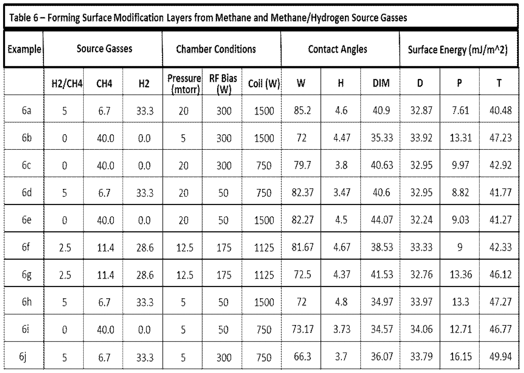


Claims
Priority Applications (6)
| Application Number | Priority Date | Filing Date | Title |
|---|---|---|---|
| KR1020167023172A KR102353030B1 (en) | 2014-01-27 | 2015-01-26 | Articles and methods for controlled bonding of thin sheets with carriers |
| CN201580015961.2A CN106132688B (en) | 2014-01-27 | 2015-01-26 | Article and method for controlled bonding of a sheet to a carrier |
| EP15740126.6A EP3099483B1 (en) | 2014-01-27 | 2015-01-26 | Articles and methods for controlled bonding of thin sheets with carriers |
| JP2016548221A JP6770432B2 (en) | 2014-01-27 | 2015-01-26 | Articles and methods for controlled binding of thin sheets to carriers |
| US15/122,366 US10046542B2 (en) | 2014-01-27 | 2015-01-26 | Articles and methods for controlled bonding of thin sheets with carriers |
| US15/921,034 US11123954B2 (en) | 2014-01-27 | 2018-03-14 | Articles and methods for controlled bonding of thin sheets with carriers |
Applications Claiming Priority (2)
| Application Number | Priority Date | Filing Date | Title |
|---|---|---|---|
| US201461931927P | 2014-01-27 | 2014-01-27 | |
| US61/931,927 | 2014-01-27 |
Related Child Applications (2)
| Application Number | Title | Priority Date | Filing Date |
|---|---|---|---|
| US15/122,366 A-371-Of-International US10046542B2 (en) | 2014-01-27 | 2015-01-26 | Articles and methods for controlled bonding of thin sheets with carriers |
| US15/921,034 Division US11123954B2 (en) | 2014-01-27 | 2018-03-14 | Articles and methods for controlled bonding of thin sheets with carriers |
Publications (1)
| Publication Number | Publication Date |
|---|---|
| WO2015112958A1 true WO2015112958A1 (en) | 2015-07-30 |
Family
ID=53682014
Family Applications (1)
| Application Number | Title | Priority Date | Filing Date |
|---|---|---|---|
| PCT/US2015/012865 WO2015112958A1 (en) | 2014-01-27 | 2015-01-26 | Articles and methods for controlled bonding of thin sheets with carriers |
Country Status (7)
| Country | Link |
|---|---|
| US (2) | US10046542B2 (en) |
| EP (1) | EP3099483B1 (en) |
| JP (1) | JP6770432B2 (en) |
| KR (1) | KR102353030B1 (en) |
| CN (1) | CN106132688B (en) |
| TW (1) | TWI671200B (en) |
| WO (1) | WO2015112958A1 (en) |
Cited By (13)
| Publication number | Priority date | Publication date | Assignee | Title |
|---|---|---|---|---|
| WO2016073658A1 (en) | 2014-11-05 | 2016-05-12 | Corning Incorporated | Bottom-up electrolytic via plating method |
| US9586858B2 (en) | 2012-10-12 | 2017-03-07 | Corning Incorporated | Laminate articles with moderate adhesion and retained strength |
| WO2017127489A1 (en) | 2016-01-21 | 2017-07-27 | Corning Incorporated | Methods for processing a substrate |
| US9725357B2 (en) | 2012-10-12 | 2017-08-08 | Corning Incorporated | Glass articles having films with moderate adhesion and retained strength |
| WO2018044837A1 (en) * | 2016-08-30 | 2018-03-08 | Corning Incorporated | Siloxane plasma polymers for sheet bonding |
| WO2018044841A1 (en) * | 2016-08-31 | 2018-03-08 | Corning Incorporated | Articles of controllably bonded sheets and methods for making same |
| WO2018081054A1 (en) * | 2016-10-25 | 2018-05-03 | Corning Incorporated | Methods and apparatus for positioning and securing glass, glass-ceramic and ceramic substrates for coating |
| US10316010B2 (en) | 2015-12-17 | 2019-06-11 | South Dakota Board Of Regents | Versatile non-destructive surface modification of carbonaceous materials and process for grafting into polymer matrices |
| US10917966B2 (en) | 2018-01-29 | 2021-02-09 | Corning Incorporated | Articles including metallized vias |
| US11167532B2 (en) | 2015-05-19 | 2021-11-09 | Corning Incorporated | Articles and methods for bonding sheets with carriers |
| US11192340B2 (en) | 2014-04-09 | 2021-12-07 | Corning Incorporated | Device modified substrate article and methods for making |
| US11331692B2 (en) | 2017-12-15 | 2022-05-17 | Corning Incorporated | Methods for treating a substrate and method for making articles comprising bonded sheets |
| US11905201B2 (en) | 2015-06-26 | 2024-02-20 | Corning Incorporated | Methods and articles including a sheet and a carrier |
Families Citing this family (37)
| Publication number | Priority date | Publication date | Assignee | Title |
|---|---|---|---|---|
| US10543662B2 (en) | 2012-02-08 | 2020-01-28 | Corning Incorporated | Device modified substrate article and methods for making |
| US8735219B2 (en) | 2012-08-30 | 2014-05-27 | Ziptronix, Inc. | Heterogeneous annealing method and device |
| US9340443B2 (en) | 2012-12-13 | 2016-05-17 | Corning Incorporated | Bulk annealing of glass sheets |
| US10510576B2 (en) | 2013-10-14 | 2019-12-17 | Corning Incorporated | Carrier-bonding methods and articles for semiconductor and interposer processing |
| WO2015112958A1 (en) | 2014-01-27 | 2015-07-30 | Corning Incorporated | Articles and methods for controlled bonding of thin sheets with carriers |
| US20160270247A1 (en) * | 2015-03-11 | 2016-09-15 | Apple Inc. | Laminating sapphire and glass using intermolecular force adhesion |
| JP6195022B2 (en) * | 2015-03-19 | 2017-09-13 | ウシオ電機株式会社 | How to bond workpieces |
| JP2018532677A (en) * | 2015-10-02 | 2018-11-08 | コーニング インコーポレイテッド | Method to reduce particle adhesion by treating glass surface |
| WO2017075151A1 (en) | 2015-10-30 | 2017-05-04 | Corning Incorporated | Methods for processing a first substrate bonded to a second substrate |
| US10410883B2 (en) * | 2016-06-01 | 2019-09-10 | Corning Incorporated | Articles and methods of forming vias in substrates |
| US10134657B2 (en) | 2016-06-29 | 2018-11-20 | Corning Incorporated | Inorganic wafer having through-holes attached to semiconductor wafer |
| US10794679B2 (en) | 2016-06-29 | 2020-10-06 | Corning Incorporated | Method and system for measuring geometric parameters of through holes |
| TWI673230B (en) | 2017-01-16 | 2019-10-01 | 昇佳電子股份有限公司 | Manufacturing method of micro-electro-mechanical systems device |
| US10580725B2 (en) | 2017-05-25 | 2020-03-03 | Corning Incorporated | Articles having vias with geometry attributes and methods for fabricating the same |
| US11078112B2 (en) | 2017-05-25 | 2021-08-03 | Corning Incorporated | Silica-containing substrates with vias having an axially variable sidewall taper and methods for forming the same |
| CN107633997B (en) * | 2017-08-10 | 2019-01-29 | 长江存储科技有限责任公司 | A kind of wafer bonding method |
| US10727195B2 (en) * | 2017-09-15 | 2020-07-28 | Technetics Group Llc | Bond materials with enhanced plasma resistant characteristics and associated methods |
| KR102304660B1 (en) * | 2017-10-18 | 2021-09-23 | 동우 화인켐 주식회사 | Flexible Display Device |
| WO2019100050A1 (en) * | 2017-11-20 | 2019-05-23 | Corning Incorporated | Temporary bonding of glass pairs using cationic surfactants and/or organic salts |
| US11554984B2 (en) | 2018-02-22 | 2023-01-17 | Corning Incorporated | Alkali-free borosilicate glasses with low post-HF etch roughness |
| US11152294B2 (en) | 2018-04-09 | 2021-10-19 | Corning Incorporated | Hermetic metallized via with improved reliability |
| US10964664B2 (en) | 2018-04-20 | 2021-03-30 | Invensas Bonding Technologies, Inc. | DBI to Si bonding for simplified handle wafer |
| WO2020010056A1 (en) * | 2018-07-03 | 2020-01-09 | Invensas Bonding Technologies, Inc. | Techniques for joining dissimilar materials in microelectronics |
| WO2020018285A1 (en) * | 2018-07-16 | 2020-01-23 | Corning Incorporated | Methods of ceramming glass articles having improved warp |
| JP7116243B2 (en) | 2018-07-16 | 2022-08-09 | コーニング インコーポレイテッド | Glass-ceramic article with improved properties and method of making same |
| WO2020018408A1 (en) | 2018-07-16 | 2020-01-23 | Corning Incorporated | Methods for ceramming glass with nucleation and growth density and viscosity changes |
| JP2020128077A (en) * | 2018-08-01 | 2020-08-27 | 東洋紡株式会社 | Laminate film, edge cleaning device, and manufacturing method of cleaned laminate film |
| KR20210038952A (en) | 2018-08-02 | 2021-04-08 | 비와이디 컴퍼니 리미티드 | Glass composite, casing, display device and terminal device |
| KR102269203B1 (en) * | 2018-08-22 | 2021-06-24 | 주식회사 엘지화학 | Mask film and method for preparing polarizing plate using same |
| JP7128697B2 (en) * | 2018-09-19 | 2022-08-31 | ファスフォードテクノロジ株式会社 | Die bonding apparatus and semiconductor device manufacturing method |
| JP2022513155A (en) * | 2018-11-30 | 2022-02-07 | コーニング インコーポレイテッド | Insulated glass unit with low CTE central plate glass |
| CN113196418A (en) * | 2018-12-20 | 2021-07-30 | 株式会社村田制作所 | Laminate, electronic component, and method for producing laminate |
| KR20210127188A (en) | 2019-02-21 | 2021-10-21 | 코닝 인코포레이티드 | Glass or glass ceramic article having copper-metalized through holes and process for making same |
| WO2021092376A1 (en) * | 2019-11-08 | 2021-05-14 | Mosaic Microsystems Llc | Processed inorganic wafer and processing wafer stack with abrasive process |
| US11673830B2 (en) * | 2020-11-11 | 2023-06-13 | Applied Materials, Inc. | Glass carrier cleaning using ozone |
| WO2022113874A1 (en) * | 2020-11-26 | 2022-06-02 | 日本電気硝子株式会社 | Method of manufacturing glass film laminate and method of washing glass sheet |
| KR102577497B1 (en) * | 2022-11-28 | 2023-09-11 | 에스케이엔펄스 주식회사 | Part for semiconductor device manufacturing apparatus, semiconductor device manufacturing apparatus including same, and manufacturing method for semiconductor device |
Citations (6)
| Publication number | Priority date | Publication date | Assignee | Title |
|---|---|---|---|---|
| US20040247949A1 (en) * | 2002-08-07 | 2004-12-09 | Kunio Akedo | Laminating product including adhesion layer and laminate product including protective film |
| US20110026236A1 (en) * | 2008-04-17 | 2011-02-03 | Asahi Glass Company, Limited | Glass laminate, display panel with support, method for producing glass laminate and method for manufacturing display panel with support |
| US20110111194A1 (en) * | 2009-05-06 | 2011-05-12 | Carre Alain R E | Carrier for glass substrates |
| US20120080403A1 (en) * | 2010-01-12 | 2012-04-05 | Masahiro Tomamoto | Glass film laminate, method of producing the same, and method of producing glass film |
| US20120202030A1 (en) * | 2009-10-20 | 2012-08-09 | Asahi Glass Company, Limited | Glass laminate, display device panel with supporting body, display device panel, display device, method for producing glass laminate, method for producing display device panel with supporting body, and method for producing display device panel |
| WO2013119737A2 (en) * | 2012-02-08 | 2013-08-15 | Corning Incorporated | Processing flexible glass with a carrier |
Family Cites Families (355)
| Publication number | Priority date | Publication date | Assignee | Title |
|---|---|---|---|---|
| GB1082116A (en) | 1964-09-03 | 1967-09-06 | Owens Illinois Inc | Organopolysiloxane resins and their production |
| US3722181A (en) | 1970-05-22 | 1973-03-27 | Du Pont | Chromatographic packing with chemically bonded organic stationary phases |
| FR2110495A5 (en) | 1970-10-19 | 1972-06-02 | Michelin & Cie | |
| IE35508B1 (en) | 1971-08-11 | 1976-03-03 | Intercontinental Chem Co Ltd | Method of forming adhesive bonds between surfaces |
| US4096315A (en) | 1976-12-15 | 1978-06-20 | The United States Of America As Represented By The Administrator Of The National Aeronautics And Space Administration | Process for producing a well-adhered durable optical coating on an optical plastic substrate |
| GB1583544A (en) | 1977-07-25 | 1981-01-28 | Uop Inc | Metal-clad laminates |
| US4179324A (en) | 1977-11-28 | 1979-12-18 | Spire Corporation | Process for fabricating thin film and glass sheet laminate |
| US4397722A (en) | 1981-12-31 | 1983-08-09 | International Business Machines Corporation | Polymers from aromatic silanes and process for their preparation |
| US4599243A (en) | 1982-12-23 | 1986-07-08 | International Business Machines Corporation | Use of plasma polymerized organosilicon films in fabrication of lift-off masks |
| US4849284A (en) | 1987-02-17 | 1989-07-18 | Rogers Corporation | Electrical substrate material |
| US4822466A (en) | 1987-06-25 | 1989-04-18 | University Of Houston - University Park | Chemically bonded diamond films and method for producing same |
| US4810326A (en) | 1987-08-31 | 1989-03-07 | International Business Machines Corporation | Interlaminate adhesion between polymeric materials and electrolytic copper surfaces |
| US5357726A (en) | 1989-02-02 | 1994-10-25 | Chemfab Corporation | Composite materials for structural end uses |
| US5141800A (en) | 1989-02-02 | 1992-08-25 | Chemical Fabrics Corporation | Method of making laminated PTFE-containing composites and products thereof |
| US4990462A (en) | 1989-04-12 | 1991-02-05 | Advanced Micro Devices, Inc. | Method for coplanar integration of semiconductor ic devices |
| US5073181A (en) | 1990-08-09 | 1991-12-17 | Corning Incorporated | Method of protecting glass surfaces using submicron refractory particles |
| CA2069038C (en) | 1991-05-22 | 1997-08-12 | Kiyofumi Sakaguchi | Method for preparing semiconductor member |
| US5462781A (en) | 1991-06-14 | 1995-10-31 | W. L. Gore & Associates, Inc. | Surface modified porous expanded polytetrafluoroethylene and process for making |
| US5222494A (en) | 1991-07-31 | 1993-06-29 | Cyberonics, Inc. | Implantable tissue stimulator output stabilization system |
| JP3039070B2 (en) | 1991-10-09 | 2000-05-08 | 住友電気工業株式会社 | Fluororesin coating |
| FR2690279B1 (en) | 1992-04-15 | 1997-10-03 | Picogiga Sa | MULTISPECTRAL PHOTOVOLTAUIC COMPONENT. |
| US5491571A (en) | 1993-01-19 | 1996-02-13 | Hughes Aircraft Company | Liquid crystal display including electrodes and driver devices integrally formed in monocrystalline semiconductor layer |
| US5482896A (en) | 1993-11-18 | 1996-01-09 | Eastman Kodak Company | Light emitting device comprising an organic LED array on an ultra thin substrate and process for forming same |
| US5616179A (en) | 1993-12-21 | 1997-04-01 | Commonwealth Scientific Corporation | Process for deposition of diamondlike, electrically conductive and electron-emissive carbon-based films |
| US5554680A (en) | 1994-02-16 | 1996-09-10 | E. I. Du Pont De Nemours And Company | Heat-resistant perfluoroelastomer composition |
| JP3081122B2 (en) | 1994-07-18 | 2000-08-28 | シャープ株式会社 | Jig for transporting substrate and method of manufacturing liquid crystal display element using the same |
| US5760100B1 (en) | 1994-09-06 | 2000-11-14 | Ciba Vision Corp | Extended wear ophthalmic lens |
| US5413940A (en) | 1994-10-11 | 1995-05-09 | Taiwan Semiconductor Manufacturing Company | Process of treating SOG layer using end-point detector for outgassing |
| DE69606942T2 (en) | 1995-09-25 | 2000-10-05 | Dow Corning | Use of pre-ceramic polymers as adhesives for electronics |
| EP0854891B1 (en) | 1995-10-13 | 2003-05-28 | Dow Global Technologies Inc. | Process for preparing coated plastic surfaces |
| US5661618A (en) | 1995-12-11 | 1997-08-26 | International Business Machines Corporation | Magnetic recording device having a improved slider |
| JP3930591B2 (en) | 1995-12-22 | 2007-06-13 | 東陶機器株式会社 | Photocatalytic hydrophilic coating composition, method for forming hydrophilic film and coated article |
| US5888591A (en) | 1996-05-06 | 1999-03-30 | Massachusetts Institute Of Technology | Chemical vapor deposition of fluorocarbon polymer thin films |
| US5989998A (en) | 1996-08-29 | 1999-11-23 | Matsushita Electric Industrial Co., Ltd. | Method of forming interlayer insulating film |
| WO2004079826A1 (en) | 1996-10-22 | 2004-09-16 | Mitsutoshi Miyasaka | Method for manufacturing thin film transistor, display, and electronic device |
| US5820991A (en) | 1997-02-24 | 1998-10-13 | Cabo; Ana M. | Fused glass sheets having ceramic paint and metal foil and method of making same |
| DE19711459A1 (en) | 1997-03-19 | 1998-09-24 | Flachglas Automotive Gmbh | Process for the production of a curved laminated safety glass pane |
| JP3551702B2 (en) | 1997-05-08 | 2004-08-11 | カシオ計算機株式会社 | Liquid crystal display device and driving method thereof |
| US6687969B1 (en) | 1997-05-16 | 2004-02-10 | Micron Technology, Inc. | Methods of fixturing flexible substrates and methods of processing flexible substrates |
| US5972152A (en) | 1997-05-16 | 1999-10-26 | Micron Communications, Inc. | Methods of fixturing flexible circuit substrates and a processing carrier, processing a flexible circuit and processing a flexible circuit substrate relative to a processing carrier |
| JPH1126733A (en) | 1997-07-03 | 1999-01-29 | Seiko Epson Corp | Transfer method of thin film device, thin film device, thin film integrated circuit device, active matrix substrate, liquid crystal display and electronic equipment |
| EP1018153A1 (en) | 1997-08-29 | 2000-07-12 | Sharon N. Farrens | In situ plasma wafer bonding method |
| US5966622A (en) | 1997-10-08 | 1999-10-12 | Lucent Technologies Inc. | Process for bonding crystalline substrates with different crystal lattices |
| US6852650B2 (en) | 1998-02-05 | 2005-02-08 | Asm Japan K.K. | Insulation film on semiconductor substrate and method for forming same |
| EP2261914A3 (en) | 1998-02-23 | 2011-03-09 | Kabushiki Kaisha Toshiba | Information storage medium, information playback method and apparatus and information recording method |
| US6159385A (en) | 1998-05-08 | 2000-12-12 | Rockwell Technologies, Llc | Process for manufacture of micro electromechanical devices having high electrical isolation |
| EP1048628A1 (en) | 1999-04-30 | 2000-11-02 | Schott Glas | Polymer coated glassfoil substrate |
| US6379746B1 (en) | 1999-02-02 | 2002-04-30 | Corning Incorporated | Method for temporarily protecting glass articles |
| JP3202718B2 (en) | 1999-02-23 | 2001-08-27 | 鹿児島日本電気株式会社 | Display device manufacturing jig and display device manufacturing method using the same |
| US6387736B1 (en) | 1999-04-26 | 2002-05-14 | Agilent Technologies, Inc. | Method and structure for bonding layers in a semiconductor device |
| US6338901B1 (en) | 1999-05-03 | 2002-01-15 | Guardian Industries Corporation | Hydrophobic coating including DLC on substrate |
| US6602606B1 (en) | 1999-05-18 | 2003-08-05 | Nippon Sheet Glass Co., Ltd. | Glass sheet with conductive film, method of manufacturing the same, and photoelectric conversion device using the same |
| US8853696B1 (en) | 1999-06-04 | 2014-10-07 | Semiconductor Energy Laboratory Co., Ltd. | Electro-optical device and electronic device |
| US6824879B2 (en) | 1999-06-10 | 2004-11-30 | Honeywell International Inc. | Spin-on-glass anti-reflective coatings for photolithography |
| SG93210A1 (en) | 1999-06-29 | 2002-12-17 | Univ Singapore | Method for lamination of fluoropolymer to metal and printed circuit board (pcb) substrate |
| TW544727B (en) | 1999-08-13 | 2003-08-01 | Semiconductor Energy Lab | Method of manufacturing a semiconductor device |
| US6674140B2 (en) | 2000-02-01 | 2004-01-06 | Analog Devices, Inc. | Process for wafer level treatment to reduce stiction and passivate micromachined surfaces and compounds used therefor |
| US6902987B1 (en) | 2000-02-16 | 2005-06-07 | Ziptronix, Inc. | Method for low temperature bonding and bonded structure |
| US6528145B1 (en) | 2000-06-29 | 2003-03-04 | International Business Machines Corporation | Polymer and ceramic composite electronic substrates |
| DE10034737C2 (en) | 2000-07-17 | 2002-07-11 | Fraunhofer Ges Forschung | Process for producing a permanent release layer by plasma polymerization on the surface of a molding tool, a molding tool which can be produced by the process and its use |
| US6649540B2 (en) | 2000-11-09 | 2003-11-18 | The Boc Group, Inc. | Organosilane CVD precursors and their use for making organosilane polymer low-k dielectric film |
| FR2823599B1 (en) | 2001-04-13 | 2004-12-17 | Commissariat Energie Atomique | DEMOMTABLE SUBSTRATE WITH CONTROLLED MECHANICAL HOLDING AND METHOD OF MAKING |
| FR2823596B1 (en) | 2001-04-13 | 2004-08-20 | Commissariat Energie Atomique | SUBSTRATE OR DISMOUNTABLE STRUCTURE AND METHOD OF MAKING SAME |
| FR2824821B1 (en) | 2001-05-17 | 2003-08-29 | Essilor Int | PROCESS FOR THE PREPARATION OF A GLASS SUITABLE FOR OVERFLOWING, GLASS THUS OBTAINED AND METHOD FOR OVERFLOWING SUCH A GLASS |
| US6956268B2 (en) | 2001-05-18 | 2005-10-18 | Reveo, Inc. | MEMS and method of manufacturing MEMS |
| US7045878B2 (en) | 2001-05-18 | 2006-05-16 | Reveo, Inc. | Selectively bonded thin film layer and substrate layer for processing of useful devices |
| JP5415658B2 (en) | 2001-05-28 | 2014-02-12 | 三菱樹脂株式会社 | Intermediate film adhesive sheet and transparent laminate |
| WO2003001616A2 (en) | 2001-06-20 | 2003-01-03 | Showa Denko K.K. | Light emitting material and organic light-emitting device |
| ATE370107T1 (en) | 2001-06-29 | 2007-09-15 | Crystal Syst | FOG-RESISTANT TRANSPARENT ARTICLES, MATERIALS THAT FORM A HYDROPHILIC INORGANIC LAYER OF HIGH HARDNESS AND METHOD FOR PRODUCING A LOW-FOG LENS |
| US6735982B2 (en) | 2001-07-12 | 2004-05-18 | Intel Corporation | Processing relatively thin glass sheets |
| US6649212B2 (en) | 2001-07-30 | 2003-11-18 | Guardian Industries Corporation | Modified silicon-based UV absorbers useful in crosslinkable polysiloxane coatings via sol-gel polymerization |
| US7351300B2 (en) | 2001-08-22 | 2008-04-01 | Semiconductor Energy Laboratory Co., Ltd. | Peeling method and method of manufacturing semiconductor device |
| JP2003077187A (en) | 2001-08-30 | 2003-03-14 | Toshiba Corp | Method for manufacturing optical disk |
| JP2003071937A (en) * | 2001-09-05 | 2003-03-12 | Toppan Printing Co Ltd | Laminated body, method for manufacturing it, and multi- layer circuit board |
| US7033910B2 (en) | 2001-09-12 | 2006-04-25 | Reveo, Inc. | Method of fabricating multi layer MEMS and microfluidic devices |
| US6528351B1 (en) | 2001-09-24 | 2003-03-04 | Jigsaw Tek, Inc. | Integrated package and methods for making same |
| US6814833B2 (en) | 2001-10-26 | 2004-11-09 | Corning Incorporated | Direct bonding of articles containing silicon |
| US6521857B1 (en) | 2001-11-19 | 2003-02-18 | Geomat Insights, Llc | Plasma enhanced bonding method and device |
| DE10162435A1 (en) | 2001-12-19 | 2003-07-17 | Joerg Lahann | Process for the production of surface coatings which reduce the adsorption of proteins or the adhesion of bacteria and / or cells |
| US6824872B2 (en) | 2002-04-23 | 2004-11-30 | Laurel Products Llc | Surface-treating fluoropolymer powders using atmospheric plasma |
| US6699798B2 (en) | 2002-04-24 | 2004-03-02 | Intel Corporation | Promoting adhesion of fluoropolymer films to semiconductor substrates |
| FR2874455B1 (en) | 2004-08-19 | 2008-02-08 | Soitec Silicon On Insulator | HEAT TREATMENT BEFORE BONDING TWO PLATES |
| JP3639978B2 (en) | 2002-05-10 | 2005-04-20 | 日本航空電子工業株式会社 | Light switch |
| DE60325669D1 (en) | 2002-05-17 | 2009-02-26 | Semiconductor Energy Lab | Method for transferring an object and method for producing a semiconductor device |
| KR101005989B1 (en) | 2002-06-11 | 2011-01-05 | 코니카 미놀타 홀딩스 가부시키가이샤 | Surface treatment method and optical part |
| US7101947B2 (en) | 2002-06-14 | 2006-09-05 | Florida State University Research Foundation, Inc. | Polyelectrolyte complex films for analytical and membrane separation of chiral compounds |
| JP3941627B2 (en) * | 2002-08-07 | 2007-07-04 | 株式会社豊田中央研究所 | Laminate with adhesion layer |
| EP1573086A4 (en) | 2002-09-18 | 2012-10-03 | Air Prod & Chem | Additives to prevent degradation of alkyl-hydrogen siloxanes |
| DE20215401U1 (en) | 2002-10-07 | 2004-02-19 | Schott Glas | Composite of a thin substrate and a carrier substrate with releasable connecting means |
| TW578439B (en) | 2002-10-25 | 2004-03-01 | Ritdisplay Corp | Organic light emitting diode and material applied in the organic light emitting diode |
| TW200421497A (en) | 2002-11-20 | 2004-10-16 | Reveo Inc | Method and system for increasing yield of vertically integrated devices |
| JP2004178891A (en) | 2002-11-26 | 2004-06-24 | Mitsubishi Electric Corp | Manufacturing method of electron emitting type light emitting device |
| DE10256247A1 (en) * | 2002-11-29 | 2004-06-09 | Andreas Jakob | Process for treating wafers comprises covering the front side of the wafer having components with a layer system consisting of a separating layer and a protective layer before the rear side of the wafer is coated |
| JP4936667B2 (en) | 2002-11-29 | 2012-05-23 | フラウンホファー ゲゼルシャフト ツール フェルドルンク デル アンゲヴァントテン フォルシュンク エー ファウ | Wafer processing process and apparatus and wafer with intermediate and carrier layers |
| US20060165975A1 (en) * | 2002-12-17 | 2006-07-27 | Moser Eva M | Substrate comprising a polar plasma-polymerised coating |
| US6762074B1 (en) | 2003-01-21 | 2004-07-13 | Micron Technology, Inc. | Method and apparatus for forming thin microelectronic dies |
| US7089635B2 (en) | 2003-02-25 | 2006-08-15 | Palo Alto Research Center, Incorporated | Methods to make piezoelectric ceramic thick film arrays and elements |
| US6964201B2 (en) | 2003-02-25 | 2005-11-15 | Palo Alto Research Center Incorporated | Large dimension, flexible piezoelectric ceramic tapes |
| TWI361814B (en) | 2003-03-07 | 2012-04-11 | Kuraray Co | Plastic bonding method |
| US7220656B2 (en) | 2003-04-29 | 2007-05-22 | Micron Technology, Inc. | Strained semiconductor by wafer bonding with misorientation |
| US6969166B2 (en) | 2003-05-29 | 2005-11-29 | 3M Innovative Properties Company | Method for modifying the surface of a substrate |
| JP2005014599A (en) * | 2003-05-30 | 2005-01-20 | Toyota Central Res & Dev Lab Inc | Resin sheet and electroluminescence display device |
| FR2855909B1 (en) | 2003-06-06 | 2005-08-26 | Soitec Silicon On Insulator | PROCESS FOR THE CONCURRENT PRODUCTION OF AT LEAST ONE PAIR OF STRUCTURES COMPRISING AT LEAST ONE USEFUL LAYER REPORTED ON A SUBSTRATE |
| US20040258850A1 (en) | 2003-06-18 | 2004-12-23 | Ann Straccia | Environmentally friendly reactive fixture to allow localized surface engineering for improved adhesion to coated and non-coated substrates |
| US20050001201A1 (en) | 2003-07-03 | 2005-01-06 | Bocko Peter L. | Glass product for use in ultra-thin glass display applications |
| FR2859312B1 (en) | 2003-09-02 | 2006-02-17 | Soitec Silicon On Insulator | MULTIFUNCTIONAL METAL SEAL |
| US7242041B2 (en) | 2003-09-22 | 2007-07-10 | Lucent Technologies Inc. | Field-effect transistors with weakly coupled layered inorganic semiconductors |
| US20050069713A1 (en) | 2003-09-30 | 2005-03-31 | Rahul Gupta | Capillary coating method |
| US6992371B2 (en) | 2003-10-09 | 2006-01-31 | Freescale Semiconductor, Inc. | Device including an amorphous carbon layer for improved adhesion of organic layers and method of fabrication |
| WO2005036604A2 (en) | 2003-10-09 | 2005-04-21 | E.I. Dupont De Nemours And Company | Apparatus and method for supporting a flexible substrate during processing |
| US20050081993A1 (en) | 2003-10-16 | 2005-04-21 | Ilkka Steven J. | Method of bonding glass |
| GB0326537D0 (en) | 2003-11-14 | 2003-12-17 | Koninkl Philips Electronics Nv | Flexible devices |
| US20050118742A1 (en) | 2003-11-17 | 2005-06-02 | Frank Henning | Method for reducing the adhesive properties of MEMS and anti-adhesion-coated device |
| GB0327093D0 (en) | 2003-11-21 | 2003-12-24 | Koninkl Philips Electronics Nv | Active matrix displays and other electronic devices having plastic substrates |
| KR101002936B1 (en) | 2003-12-17 | 2010-12-21 | 삼성전자주식회사 | Carrier plate, method of laminating plastic plate using the same, and method of manufacturing display device having the flexibility |
| US7220497B2 (en) | 2003-12-18 | 2007-05-22 | Lam Research Corporation | Yttria-coated ceramic components of semiconductor material processing apparatuses and methods of manufacturing the components |
| KR101073032B1 (en) | 2003-12-19 | 2011-10-12 | 삼성전자주식회사 | Method of laminating the plastic plate method of manufacturing display device having the flexibility using the same |
| US7041608B2 (en) | 2004-02-06 | 2006-05-09 | Eastman Kodak Company | Providing fluorocarbon layers on conductive electrodes in making electronic devices such as OLED devices |
| US7147891B2 (en) | 2004-02-11 | 2006-12-12 | Dionex Corporation | Polymer substrate coated with weak cationic-exchange functional layer |
| CN1998087B (en) | 2004-03-12 | 2014-12-31 | 独立行政法人科学技术振兴机构 | Amorphous oxide and thin film transistor |
| US7087134B2 (en) * | 2004-03-31 | 2006-08-08 | Hewlett-Packard Development Company, L.P. | System and method for direct-bonding of substrates |
| JP2005300972A (en) | 2004-04-13 | 2005-10-27 | Seiko Epson Corp | Method for manufacturing display device and substrate sticking device |
| JP2006003684A (en) | 2004-06-18 | 2006-01-05 | Nikon Corp | Manufacturing method of substrateless filter |
| ITMI20041252A1 (en) | 2004-06-22 | 2004-09-22 | Solvay Solexis Spa | PERFLUOROELASTOMERIC COMPOSITIONS |
| US7261793B2 (en) | 2004-08-13 | 2007-08-28 | Hewlett-Packard Development Company, L.P. | System and method for low temperature plasma-enhanced bonding |
| US20060134362A1 (en) | 2004-12-17 | 2006-06-22 | 3M Innovative Properties Company | Optically clear pressure sensitive adhesive |
| EP1854136A1 (en) | 2005-03-01 | 2007-11-14 | Dow Corning Corporation | Temporary wafer bonding method for semiconductor processing |
| US8043697B2 (en) | 2005-04-19 | 2011-10-25 | Ube Industries, Ltd. | Polyimide film-laminated body |
| US20060246218A1 (en) | 2005-04-29 | 2006-11-02 | Guardian Industries Corp. | Hydrophilic DLC on substrate with barrier discharge pyrolysis treatment |
| TWI402935B (en) | 2005-05-17 | 2013-07-21 | Koninkl Philips Electronics Nv | Colour active martix displays |
| US7462552B2 (en) | 2005-05-23 | 2008-12-09 | Ziptronix, Inc. | Method of detachable direct bonding at low temperatures |
| US20070020451A1 (en) | 2005-07-20 | 2007-01-25 | 3M Innovative Properties Company | Moisture barrier coatings |
| US7166520B1 (en) | 2005-08-08 | 2007-01-23 | Silicon Genesis Corporation | Thin handle substrate method and structure for fabricating devices using one or more films provided by a layer transfer process |
| EP1914066B1 (en) | 2005-08-09 | 2016-09-07 | Asahi Glass Company, Limited | Thin sheet glass laminate and method for manufacturing display using thin sheet glass laminate |
| US20070048530A1 (en) | 2005-08-29 | 2007-03-01 | Wen-Kuang Tsao | Anti-static substrate |
| TWI288493B (en) | 2005-09-13 | 2007-10-11 | Ind Tech Res Inst | Method for fabricating a device with flexible substrate and method for stripping flexible-substrate |
| US7462551B2 (en) | 2005-09-30 | 2008-12-09 | Intel Corporation | Adhesive system for supporting thin silicon wafer |
| US8039049B2 (en) | 2005-09-30 | 2011-10-18 | Tokyo Electron Limited | Treatment of low dielectric constant films using a batch processing system |
| US7901743B2 (en) | 2005-09-30 | 2011-03-08 | Tokyo Electron Limited | Plasma-assisted vapor phase treatment of low dielectric constant films using a batch processing system |
| JP2007138144A (en) | 2005-10-18 | 2007-06-07 | Hitachi Chem Co Ltd | Silica-based coated film-forming composition |
| KR20070047114A (en) | 2005-11-01 | 2007-05-04 | 주식회사 엘지화학 | Manufacturing method of device with flexible substrate and device with flexible substrate manufactured by the same |
| CN101305315B (en) | 2005-11-11 | 2010-05-19 | 株式会社半导体能源研究所 | Method for forming layer having functionality and method for preparing semiconductor device |
| FR2893750B1 (en) | 2005-11-22 | 2008-03-14 | Commissariat Energie Atomique | METHOD FOR MANUFACTURING SCREEN TYPE FLEXIBLE ELECTRONIC DEVICE COMPRISING A PLURALITY OF THIN FILM COMPONENTS |
| US20070134784A1 (en) | 2005-12-09 | 2007-06-14 | Halverson Kurt J | Microreplicated microarrays |
| EP1818860B1 (en) | 2006-02-08 | 2011-03-30 | Semiconductor Energy Laboratory Co., Ltd. | RFID device |
| KR100831562B1 (en) | 2006-03-23 | 2008-05-21 | 주식회사 엘지화학 | Pressure Sensitive Adhesive Composition for Transferring Flexible Substrate |
| US7909928B2 (en) | 2006-03-24 | 2011-03-22 | The Regents Of The University Of Michigan | Reactive coatings for regioselective surface modification |
| US7737035B1 (en) | 2006-03-31 | 2010-06-15 | Novellus Systems, Inc. | Dual seal deposition process chamber and process |
| US20070248809A1 (en) | 2006-04-19 | 2007-10-25 | Steven Vincent Haldeman | Interlayers Comprising Stable Infrared Absorbing Agents |
| WO2007121524A1 (en) | 2006-04-20 | 2007-11-01 | Epitactix Pty Ltd. | Method of manufacture and resulting structures for semiconductor devices |
| EP2025650A1 (en) | 2006-05-08 | 2009-02-18 | Asahi Glass Company, Limited | Thin-sheet glass laminate, process for manufacturing display apparatus using the laminate, and supporting glass substrate |
| KR101358255B1 (en) | 2006-06-27 | 2014-02-05 | 엘지디스플레이 주식회사 | Hydrophobic mold of photo-curable type and manufacturing method for the same |
| JPWO2008007622A1 (en) | 2006-07-12 | 2009-12-10 | 旭硝子株式会社 | Glass substrate with protective glass, display device manufacturing method using glass substrate with protective glass, and silicone for release paper |
| US8084103B2 (en) | 2006-08-15 | 2011-12-27 | Sakhrani Vinay G | Method for treating a hydrophilic surface |
| US20080044588A1 (en) | 2006-08-15 | 2008-02-21 | Sakhrani Vinay G | Method for Treating a Hydrophilic Surface |
| JP2008072087A (en) | 2006-08-16 | 2008-03-27 | Kyoto Univ | Semiconductor device and manufacturing method of the semiconductor device, and display device |
| WO2008044884A1 (en) | 2006-10-13 | 2008-04-17 | Sunwoo Amc Co., Ltd. | Laminating film of plastic/teflon-silicon and method for preparing the same |
| GB0620955D0 (en) | 2006-10-20 | 2006-11-29 | Speakman Stuart P | Methods and apparatus for the manufacture of microstructures |
| US7903083B2 (en) | 2006-11-13 | 2011-03-08 | Motorola Mobility, Inc. | Mixed-mode encapsulated electrophoretic display for electronic device |
| JP5008381B2 (en) | 2006-11-15 | 2012-08-22 | 富士フイルム株式会社 | Method for producing organic electroluminescence light-emitting panel using flexible substrate, organic electroluminescence light-emitting panel produced thereby, and supporting substrate used for production thereof |
| US8069229B2 (en) | 2006-12-28 | 2011-11-29 | Computer Associates Think, Inc. | Topology static zones |
| KR100890250B1 (en) | 2007-01-08 | 2009-03-24 | 포항공과대학교 산학협력단 | Method of manufacturing a flexible device and method of manufacturing a flexible display |
| US8110906B2 (en) | 2007-01-23 | 2012-02-07 | Infineon Technologies Ag | Semiconductor device including isolation layer |
| JP5532918B2 (en) | 2007-03-12 | 2014-06-25 | 旭硝子株式会社 | Method for manufacturing display device using glass substrate with protective glass |
| JP5277552B2 (en) | 2007-03-19 | 2013-08-28 | 富士通セミコンダクター株式会社 | Manufacturing method of semiconductor device |
| US8399047B2 (en) | 2007-03-22 | 2013-03-19 | The Regents Of The Univeristy Of Michigan | Multifunctional CVD coatings |
| EP2150556B1 (en) | 2007-04-26 | 2011-01-12 | Basf Se | Silanes containing phenothiazine-s-oxide or phenothiazine-s,s-dioxide groups and the use thereof in oleds |
| US7635617B2 (en) | 2007-04-27 | 2009-12-22 | Semiconductor Energy Laboratory Co., Ltd. | Manufacturing method of semiconductor substrate and manufacturing method of semiconductor device |
| US7960916B2 (en) | 2007-05-16 | 2011-06-14 | Advanced Lcd Technologies Development Center Co., Ltd. | Display device and electronic device using thin-film transistors formed on semiconductor thin films which are crystallized on insulating substrates |
| WO2008156176A1 (en) | 2007-06-20 | 2008-12-24 | Asahi Glass Company, Limited | Method for treatment of surface of oxide glass with fluorinating agent |
| KR20080113576A (en) | 2007-06-25 | 2008-12-31 | 엘지디스플레이 주식회사 | Liquid crystal display device and method for fabricating thereof |
| KR101565176B1 (en) | 2007-06-25 | 2015-11-02 | 브레우어 사이언스 인코포레이션 | High-temperature spin-on temporary bonding compositions |
| TW200907003A (en) | 2007-07-03 | 2009-02-16 | Hitachi Chemical Co Ltd | Adhesive composition and method of manufacturing thereof, adhesive member using the adhesive composition and method of manufacturing thereof, supporting member for mounting semiconductor and method of manufacturing thereof, and semiconductor apparatus an |
| JP2009035721A (en) | 2007-07-11 | 2009-02-19 | Seiko Epson Corp | Substrate with joining film, joining method and joined product |
| JP2009028923A (en) | 2007-07-24 | 2009-02-12 | Seiko Epson Corp | Joining method, joint article and wiring board |
| JP2009028922A (en) | 2007-07-24 | 2009-02-12 | Seiko Epson Corp | Joining method, joint article, droplet ejection head and droplet ejection device |
| JP2009074002A (en) * | 2007-09-21 | 2009-04-09 | Seiko Epson Corp | Adhesion sheet, joining method and joined body |
| US20090091025A1 (en) | 2007-10-04 | 2009-04-09 | Agency For Science, Technology And Research | Method for forming and releasing interconnects |
| US9056951B2 (en) | 2007-10-05 | 2015-06-16 | The Regents Of The University Of Michigan | Ultrastrong and stiff layered polymer nanocomposites and hierarchical laminate materials thereof |
| JP4710897B2 (en) * | 2007-11-28 | 2011-06-29 | セイコーエプソン株式会社 | Separation method of joined body |
| KR101445734B1 (en) | 2007-12-07 | 2014-10-01 | 삼성전자 주식회사 | Liquid Crystal Display |
| RU2010129076A (en) | 2008-01-24 | 2012-01-20 | Брюэр Сайенс Инк. (Us) | METHOD OF REVERSABLE FIXING OF A SEMICONDUCTOR PLATE WITH FORMED DEVICES TO A CARRYING SUBSTRATE |
| JP5024087B2 (en) | 2008-02-05 | 2012-09-12 | 旭硝子株式会社 | GLASS LAMINATE, PANEL FOR DISPLAY DEVICE WITH SUPPORT AND METHOD FOR PRODUCING THEM |
| EP2244878B1 (en) | 2008-02-05 | 2018-11-07 | Saint-Gobain Performance Plastics Corporation | Multi-layer article |
| GB0802912D0 (en) | 2008-02-15 | 2008-03-26 | Carben Semicon Ltd | Thin-film transistor, carbon-based layer and method of production thereof |
| KR20090095026A (en) | 2008-03-04 | 2009-09-09 | 삼성전자주식회사 | Method of manufacturing for display device |
| CN101980861B (en) | 2008-04-08 | 2014-08-06 | 亚利桑那董事会,代表亚利桑那州立大学行事的亚利桑那州法人团体 | Assemblies and methods for reducing warp and bow of a flexible substrate during semiconductor processing |
| KR101500684B1 (en) | 2008-04-17 | 2015-03-10 | 삼성디스플레이 주식회사 | Carrier glasses and menufacturing method of flexible display device using the same |
| US7842548B2 (en) | 2008-04-22 | 2010-11-30 | Taiwan Semconductor Manufacturing Co., Ltd. | Fixture for P-through silicon via assembly |
| KR101458901B1 (en) | 2008-04-29 | 2014-11-10 | 삼성디스플레이 주식회사 | Method of manufacturing flexible display device |
| US7960840B2 (en) | 2008-05-12 | 2011-06-14 | Texas Instruments Incorporated | Double wafer carrier process for creating integrated circuit die with through-silicon vias and micro-electro-mechanical systems protected by a hermetic cavity created at the wafer level |
| JP2009283155A (en) | 2008-05-19 | 2009-12-03 | Seiko Epson Corp | Manufacturing method of display device, display device, and electronic apparatus |
| JP5029523B2 (en) | 2008-07-14 | 2012-09-19 | 旭硝子株式会社 | GLASS LAMINATE, PANEL FOR DISPLAY DEVICE WITH SUPPORT, PANEL FOR DISPLAY DEVICE, DISPLAY DEVICE AND MANUFACTURING METHOD THEREOF |
| DE102008045370B4 (en) | 2008-09-02 | 2010-07-08 | Grenzebach Maschinenbau Gmbh | Method and device for transporting large-area, thin glass plates |
| US20110311789A1 (en) | 2008-09-12 | 2011-12-22 | Arizona Board of Regents, a body corporate acting for and on behalf of Arizona State University | Methods for Attaching Flexible Substrates to Rigid Carriers and Resulting Devices |
| TWI354854B (en) | 2008-09-15 | 2011-12-21 | Ind Tech Res Inst | Substrate structures applied in flexible electrica |
| JP2010107597A (en) | 2008-10-28 | 2010-05-13 | Seiko Epson Corp | Optical element and method for producing same |
| KR101555551B1 (en) | 2008-11-07 | 2015-09-24 | 엘지디스플레이 주식회사 | Method for fabricating flexible display device |
| CN102272231B (en) | 2008-11-19 | 2013-10-30 | 陶氏康宁公司 | Silicone composition and method for preparing same |
| US8211270B2 (en) | 2008-11-21 | 2012-07-03 | Nitto Denko Corporation | Method of detaching attached boards from each other |
| KR101572814B1 (en) | 2008-12-05 | 2015-12-01 | 코닌클리케 필립스 엔.브이. | Electronic devices having plastic substrates |
| DE102009022628A1 (en) | 2008-12-05 | 2010-06-10 | Evonik Goldschmidt Gmbh | Method for modifying surfaces |
| US9063605B2 (en) | 2009-01-09 | 2015-06-23 | Apple Inc. | Thin glass processing using a carrier |
| TW201033000A (en) | 2009-01-09 | 2010-09-16 | Asahi Glass Co Ltd | Glass laminate and manufacturing method therefor |
| JP5207306B2 (en) | 2009-01-26 | 2013-06-12 | 武井電機工業株式会社 | Thin film removal method and apparatus for thin film laminated glass substrate |
| WO2010098762A1 (en) | 2009-02-27 | 2010-09-02 | Exxonmobil Oil Corporation | Plasma treated evoh multilayer film |
| TWI410329B (en) | 2009-03-09 | 2013-10-01 | Ind Tech Res Inst | Apparatus for releasing a flexible device and method thereof |
| JP5402184B2 (en) | 2009-04-13 | 2014-01-29 | 日本電気硝子株式会社 | Glass film and method for producing the same |
| CN101873532B (en) | 2009-04-22 | 2013-01-02 | 电信科学技术研究院 | Method, base station and UE (User End) for sending and acquiring control information in multicast broadcast system |
| WO2010128611A1 (en) | 2009-05-08 | 2010-11-11 | 日立化成工業株式会社 | Film-like adhesive agent for sealing semiconductor, semiconductor device, and process for manufacturing the semiconductor device |
| WO2010141257A2 (en) | 2009-06-03 | 2010-12-09 | Applied Materials, Inc. | Method and apparatus for etching |
| CN101924067B (en) | 2009-06-09 | 2013-05-08 | 财团法人工业技术研究院 | Method for separating flexible membrane from carrier plate and manufacturing method of flexible electronic device |
| JP2010284869A (en) | 2009-06-11 | 2010-12-24 | Shin-Etsu Chemical Co Ltd | Joining member |
| JP5594522B2 (en) | 2009-07-03 | 2014-09-24 | 日本電気硝子株式会社 | Glass film laminate for manufacturing electronic devices |
| US7987566B2 (en) | 2009-07-15 | 2011-08-02 | Sturzebecher Richard J | Capacitor forming method |
| US8568184B2 (en) | 2009-07-15 | 2013-10-29 | Apple Inc. | Display modules |
| CN101989469A (en) | 2009-07-31 | 2011-03-23 | 群康科技(深圳)有限公司 | Current-conducting plate |
| US8048794B2 (en) | 2009-08-18 | 2011-11-01 | International Business Machines Corporation | 3D silicon-silicon die stack structure and method for fine pitch interconnection and vertical heat transport |
| DE102009028640A1 (en) | 2009-08-19 | 2011-02-24 | Evonik Goldschmidt Gmbh | Curable composition containing urethane-containing silylated polymers and their use in sealants and adhesives, binders and / or surface modifiers |
| JP2011048979A (en) | 2009-08-26 | 2011-03-10 | Canon Inc | Image display apparatus |
| WO2011024690A1 (en) | 2009-08-27 | 2011-03-03 | 旭硝子株式会社 | Multilayer structure with flexible base material and support, panel for use in electronic device provided with support and production method for panel for use in electronic device |
| US9847243B2 (en) | 2009-08-27 | 2017-12-19 | Corning Incorporated | Debonding a glass substrate from carrier using ultrasonic wave |
| JP5562597B2 (en) | 2009-08-28 | 2014-07-30 | 荒川化学工業株式会社 | SUPPORT, GLASS SUBSTRATE LAMINATE, DISPLAY DEVICE PANEL WITH SUPPORT AND METHOD FOR PRODUCING DISPLAY DEVICE PANEL |
| KR101723254B1 (en) | 2009-09-08 | 2017-04-04 | 도요보 가부시키가이샤 | Glass/resin laminate, and electronic device using same |
| JP2011058579A (en) | 2009-09-10 | 2011-03-24 | Tokyo Institute Of Technology | Energy absorption structure |
| WO2011029752A1 (en) | 2009-09-11 | 2011-03-17 | Loctite (R & D) Limited | Compositions for polymer bonding |
| CN102471129B (en) | 2009-09-18 | 2015-04-15 | 日本电气硝子株式会社 | Method for producing glass film, method for treating glass film and glass film laminate |
| CN102576106B (en) | 2009-10-20 | 2015-02-11 | 旭硝子株式会社 | Glass laminate, glass laminate manufacturing method, display panel manufacturing method, and display panel obtained by means of display panel manufacturing method |
| KR101617280B1 (en) | 2009-10-21 | 2016-05-03 | 엘지디스플레이 주식회사 | Methode of fabricating display device using flexible plastic substrate |
| KR20110043376A (en) | 2009-10-21 | 2011-04-27 | 엘지디스플레이 주식회사 | Electrophoretic display device and method of fabricating the same |
| KR20110045136A (en) | 2009-10-26 | 2011-05-04 | 주식회사 삼영테크놀로지 | Coating method for separating display panel from window |
| US9019211B2 (en) | 2009-10-30 | 2015-04-28 | Corning Incorporated | Methods and apparatus for providing touch sensitive displays |
| KR101635914B1 (en) | 2009-12-16 | 2016-07-05 | 엘지디스플레이 주식회사 | Method of fabricating flexible display device |
| CA2784967A1 (en) | 2009-12-17 | 2011-07-14 | Ceramtec Gmbh | Surface conditioning for improving bone cement adhesion to ceramic substrates |
| JP2011159697A (en) | 2010-01-29 | 2011-08-18 | Dainippon Printing Co Ltd | Thin film transistor mounting substrate, method of manufacturing the same, and image display device |
| US8995146B2 (en) | 2010-02-23 | 2015-03-31 | Semblant Limited | Electrical assembly and method |
| JP2011201977A (en) | 2010-03-24 | 2011-10-13 | Seiko Epson Corp | Bonding method |
| JP2011201976A (en) | 2010-03-24 | 2011-10-13 | Seiko Epson Corp | Bonding method |
| US8349727B2 (en) | 2010-04-08 | 2013-01-08 | Liang Guo | Integrated method for high-density interconnection of electronic components through stretchable interconnects |
| US20110256385A1 (en) | 2010-04-15 | 2011-10-20 | Seiko Epson Corporation | Bonding film-attached substrate and bonding film-attached substrate manufacturing method |
| JP5625470B2 (en) | 2010-05-10 | 2014-11-19 | セイコーエプソン株式会社 | Joining method |
| JP5835214B2 (en) | 2010-05-11 | 2015-12-24 | 旭硝子株式会社 | LAMINATE MANUFACTURING METHOD AND LAMINATE |
| JP2011235556A (en) * | 2010-05-11 | 2011-11-24 | Seiko Epson Corp | Excitation energy specification method and apparatus, and bonding method and apparatus |
| JP5516046B2 (en) | 2010-05-11 | 2014-06-11 | セイコーエプソン株式会社 | Bonding film transfer sheet and bonding method |
| JP2011248011A (en) | 2010-05-25 | 2011-12-08 | Bridgestone Corp | Particle for display medium and information display panel using the same |
| GB2481187B (en) | 2010-06-04 | 2014-10-29 | Plastic Logic Ltd | Processing substrates |
| KR101721414B1 (en) | 2010-06-09 | 2017-03-31 | 삼성디스플레이 주식회사 | Backlight assembly and liquid crystal display apparatus including the same |
| US8852391B2 (en) | 2010-06-21 | 2014-10-07 | Brewer Science Inc. | Method and apparatus for removing a reversibly mounted device wafer from a carrier substrate |
| TWI432835B (en) | 2010-06-24 | 2014-04-01 | Au Optronics Corp | Flexible display panel and method of fabricating the same |
| DE102010025967B4 (en) | 2010-07-02 | 2015-12-10 | Schott Ag | Method for producing a multiplicity of holes, device for this and glass interposer |
| CN101916022B (en) | 2010-07-06 | 2012-10-10 | 友达光电股份有限公司 | Flexible display panel and manufacturing method thereof |
| CN102770268B (en) | 2010-07-28 | 2016-05-11 | 日本电气硝子株式会社 | Glass film laminate |
| JP5602529B2 (en) | 2010-07-29 | 2014-10-08 | 日本合成化学工業株式会社 | Manufacturing method of laminate, manufacturing method of polarizing plate with glass substrate, and polarizing plate with glass substrate obtained thereby |
| US20120035309A1 (en) | 2010-08-06 | 2012-02-09 | Baker Hughes Incorporated | Method to disperse nanoparticles into elastomer and articles produced therefrom |
| US9263314B2 (en) | 2010-08-06 | 2016-02-16 | Brewer Science Inc. | Multiple bonding layers for thin-wafer handling |
| JP5462107B2 (en) | 2010-08-09 | 2014-04-02 | 株式会社日本製鋼所 | Method and apparatus for manufacturing hollow molded article |
| US8846499B2 (en) | 2010-08-17 | 2014-09-30 | Taiwan Semiconductor Manufacturing Company, Ltd. | Composite carrier structure |
| TWI446420B (en) | 2010-08-27 | 2014-07-21 | Advanced Semiconductor Eng | Releasing carrier method for semiconductor process |
| US20120063952A1 (en) | 2010-09-10 | 2012-03-15 | Hong Keith C | Uv resistant clear laminates |
| KR101164945B1 (en) | 2010-09-13 | 2012-07-12 | 한국과학기술원 | Fabrication Method of Flexible Devices |
| KR101779586B1 (en) | 2010-09-27 | 2017-10-10 | 엘지디스플레이 주식회사 | Method of fabricating display device using flexible plastic substrate |
| JP5899220B2 (en) | 2010-09-29 | 2016-04-06 | ポスコ | Method for manufacturing flexible electronic device using roll-shaped mother substrate, flexible electronic device, and flexible substrate |
| US8822306B2 (en) | 2010-09-30 | 2014-09-02 | Infineon Technologies Ag | Method for manufacturing a composite wafer having a graphite core, and composite wafer having a graphite core |
| KR101267529B1 (en) | 2010-10-30 | 2013-05-24 | 엘지디스플레이 주식회사 | Method of fabricating flexible organic electro luminescent device |
| US8859103B2 (en) | 2010-11-05 | 2014-10-14 | Joseph Eugene Canale | Glass wafers for semiconductor fabrication processes and methods of making same |
| CN102034746B (en) | 2010-11-08 | 2013-06-05 | 昆山工研院新型平板显示技术中心有限公司 | Manufacturing method of active matrix organic light-emitting display array base plate |
| KR101295532B1 (en) | 2010-11-11 | 2013-08-12 | 엘지디스플레이 주식회사 | Method for manufacturing Flexible Flat Device |
| KR101271838B1 (en) | 2010-11-24 | 2013-06-07 | 주식회사 포스코 | Method of manufacturing flexible electronic device, flexibleelectronic device and flexible substrate using a reinforcing substrate |
| KR101842134B1 (en) | 2010-11-26 | 2018-03-26 | 엘지디스플레이 주식회사 | Electrophoretic Display Device and Method for Manufacturing The Same |
| EP2458620B1 (en) | 2010-11-29 | 2021-12-01 | IHP GmbH-Innovations for High Performance Microelectronics / Leibniz-Institut für innovative Mikroelektronik | Fabrication of graphene electronic devices using step surface contour |
| TW201238014A (en) | 2010-11-30 | 2012-09-16 | Corning Inc | Methods of forming a glass wiring board substrate |
| KR101049380B1 (en) | 2010-12-21 | 2011-07-15 | 한국기계연구원 | Tsv for 3d packaging of semiconductor device and fabrication method thereof |
| CN102070120B (en) | 2010-12-31 | 2012-09-05 | 东南大学 | Preparation method for high-density interposer for microelectronic system-in-package |
| CN103348464B (en) | 2011-01-26 | 2016-01-13 | 株式会社半导体能源研究所 | Semiconductor device and manufacture method thereof |
| CN102548758B (en) | 2011-02-01 | 2013-11-20 | 株式会社微龙技术研究所 | Thin-sheet glass substrate laminate and method of manufacturing the same |
| JP2012166999A (en) | 2011-02-16 | 2012-09-06 | Asahi Glass Co Ltd | Method for manufacturing glass substrate for interposer, method for manufacturing interposer, glass substrate for interposer, and interposer |
| KR101918284B1 (en) | 2011-03-03 | 2019-01-30 | 엘지디스플레이 주식회사 | Method of manufacturing a flexible display device |
| JP5355618B2 (en) | 2011-03-10 | 2013-11-27 | 三星ディスプレイ株式會社 | Flexible display device and manufacturing method thereof |
| JP2012209545A (en) | 2011-03-17 | 2012-10-25 | Sekisui Chem Co Ltd | Manufacturing method of semiconductor laminate |
| TWI445626B (en) | 2011-03-18 | 2014-07-21 | Eternal Chemical Co Ltd | Method for fabricating a flexible device |
| JP2012227310A (en) | 2011-04-19 | 2012-11-15 | Panasonic Corp | Ceramic multilayer substrate, and method of manufacturing the same |
| JPWO2012144499A1 (en) * | 2011-04-22 | 2014-07-28 | 旭硝子株式会社 | Laminate, production method and use thereof |
| JP5760696B2 (en) | 2011-05-27 | 2015-08-12 | 株式会社デンソー | Image recognition device |
| JP5862238B2 (en) | 2011-05-27 | 2016-02-16 | 東洋紡株式会社 | LAMINATE, MANUFACTURING METHOD THEREOF, AND DEVICE STRUCTURE MANUFACTURING METHOD USING THE SAME |
| JP5862866B2 (en) | 2011-05-30 | 2016-02-16 | 東洋紡株式会社 | Method for producing laminate and method for producing film device using the laminate |
| JP5883236B2 (en) | 2011-06-10 | 2016-03-09 | 日東電工株式会社 | Carrier material for thin layer substrate |
| KR20130000211A (en) | 2011-06-22 | 2013-01-02 | 삼성전자주식회사 | Methods for processing substrates |
| KR20130003997A (en) | 2011-07-01 | 2013-01-09 | 엘지디스플레이 주식회사 | Separation-combination method of carrier substrate and slim glass |
| WO2013006865A2 (en) | 2011-07-07 | 2013-01-10 | Brewer Science Inc. | Methods of transferring device wafers or layers between carrier substrates and other surfaces |
| US8617925B2 (en) | 2011-08-09 | 2013-12-31 | Soitec | Methods of forming bonded semiconductor structures in 3D integration processes using recoverable substrates, and bonded semiconductor structures formed by such methods |
| US8383460B1 (en) | 2011-09-23 | 2013-02-26 | GlobalFoundries, Inc. | Method for fabricating through substrate vias in semiconductor substrate |
| EP2761051B1 (en) | 2011-09-27 | 2018-11-07 | Applied Materials, Inc. | Carrier for thin glass substrates and use thereof |
| JP5796449B2 (en) | 2011-10-12 | 2015-10-21 | 旭硝子株式会社 | Manufacturing method of electronic device, manufacturing method of carrier substrate with resin layer |
| JP5790392B2 (en) | 2011-10-12 | 2015-10-07 | 旭硝子株式会社 | Manufacturing method of electronic device |
| KR101973826B1 (en) | 2011-10-18 | 2019-08-26 | 에이지씨 가부시키가이샤 | Laminate, method for producing laminate, and method for producing glass substrate having member for electronic devices attached thereto |
| KR101820171B1 (en) | 2011-10-24 | 2018-01-19 | 엘지디스플레이 주식회사 | Method of fabricating lightweight and thin liquid crystal display device |
| US8696864B2 (en) | 2012-01-26 | 2014-04-15 | Promerus, Llc | Room temperature debonding composition, method and stack |
| US8550061B2 (en) | 2012-01-26 | 2013-10-08 | Maruzen Company Limited | Toy gun |
| US8975157B2 (en) | 2012-02-08 | 2015-03-10 | Advanced Semiconductor Engineering, Inc. | Carrier bonding and detaching processes for a semiconductor wafer |
| US10543662B2 (en) | 2012-02-08 | 2020-01-28 | Corning Incorporated | Device modified substrate article and methods for making |
| US9725357B2 (en) | 2012-10-12 | 2017-08-08 | Corning Incorporated | Glass articles having films with moderate adhesion and retained strength |
| JP2013184346A (en) | 2012-03-07 | 2013-09-19 | Asahi Glass Co Ltd | Glass laminate, and method for producing electronic device |
| JP2013184872A (en) | 2012-03-09 | 2013-09-19 | Nippon Electric Glass Co Ltd | Edge treatment method of glass substrate, edge treatment device for glass substrate, and glass substrate |
| KR101390212B1 (en) | 2012-03-14 | 2014-05-14 | 한양대학교 에리카산학협력단 | Preparation method for gliadin nanoparticles by electrospray |
| JP2013207084A (en) | 2012-03-28 | 2013-10-07 | Sumitomo Electric Ind Ltd | Substrate module with radiator plate and method of manufacturing the same |
| JP2013216513A (en) | 2012-04-05 | 2013-10-24 | Nippon Electric Glass Co Ltd | Method for cutting glass film and glass film lamination body |
| EP2650938A1 (en) | 2012-04-13 | 2013-10-16 | Acreo Swedish ICT AB | Organic Field-Effect Transistor Device |
| JP2013224475A (en) | 2012-04-23 | 2013-10-31 | Shimazu Kogyo Kk | Particle for thermal spraying, method for forming thermally sprayed coating film, and thermally sprayed member |
| DE102012207149A1 (en) | 2012-04-27 | 2013-10-31 | Fraunhofer-Gesellschaft zur Förderung der angewandten Forschung e.V. | Composite with temporary protective film |
| KR20150023312A (en) | 2012-05-29 | 2015-03-05 | 아사히 가라스 가부시키가이샤 | Glass laminate and method for manufacturing electronic device |
| KR20130095605A (en) | 2012-06-22 | 2013-08-28 | 코스텍시스템(주) | Apparatus for bonding and debonding between device wafer and carrier wafer for semiconductor manufacturing |
| CN102815052B (en) | 2012-06-29 | 2016-08-24 | 法国圣戈班玻璃公司 | Super-hydrophobic anti-reflection substrate and preparation method thereof |
| JP2014019597A (en) | 2012-07-17 | 2014-02-03 | Nippon Electric Glass Co Ltd | Method for producing glass film, and glass film laminate |
| US9139469B2 (en) | 2012-07-17 | 2015-09-22 | Corning Incorporated | Ion exchangeable Li-containing glass compositions for 3-D forming |
| CN102789125B (en) | 2012-07-27 | 2013-11-13 | 京东方科技集团股份有限公司 | Mask plate, mat manufacturing method and LCD panel |
| CN104781201A (en) | 2012-08-17 | 2015-07-15 | 康宁股份有限公司 | Ultra-thin strengthened glasses |
| CN102820262A (en) | 2012-09-05 | 2012-12-12 | 江苏物联网研究发展中心 | Glass through hole manufacturing and interconnecting method |
| WO2014050798A1 (en) | 2012-09-28 | 2014-04-03 | Hoya株式会社 | Cover glass for electronic instrument and method for manufacturing same |
| KR101949561B1 (en) | 2012-10-12 | 2019-02-18 | 코닝 인코포레이티드 | Articles having retained strength |
| US20140150244A1 (en) | 2012-11-30 | 2014-06-05 | General Electric Company | Adhesive-free carrier assemblies for glass substrates |
| CN103035490A (en) | 2012-12-11 | 2013-04-10 | 京东方科技集团股份有限公司 | Preparation method for flexible display device |
| US9340443B2 (en) | 2012-12-13 | 2016-05-17 | Corning Incorporated | Bulk annealing of glass sheets |
| US10014177B2 (en) | 2012-12-13 | 2018-07-03 | Corning Incorporated | Methods for processing electronic devices |
| TWI617437B (en) * | 2012-12-13 | 2018-03-11 | 康寧公司 | Facilitated processing for controlling bonding between sheet and carrier |
| US10086584B2 (en) * | 2012-12-13 | 2018-10-02 | Corning Incorporated | Glass articles and methods for controlled bonding of glass sheets with carriers |
| EP2932496A4 (en) * | 2012-12-13 | 2016-11-02 | Corning Inc | Glass and methods of making glass articles |
| KR102046534B1 (en) | 2013-01-25 | 2019-11-19 | 삼성전자주식회사 | Methods for processing substrates |
| WO2014137801A1 (en) | 2013-03-03 | 2014-09-12 | John Moore | Temporary adhesive with tunable adhesion force sufficient for processing thin solid materials |
| WO2014164206A1 (en) | 2013-03-09 | 2014-10-09 | John Moore | Aqueous detergent soluble coating and adhesive and methods of temporary bonding for manufacturing |
| KR102239613B1 (en) * | 2013-03-15 | 2021-04-13 | 코닝 인코포레이티드 | Bulk annealing of glass sheets |
| KR101432575B1 (en) | 2013-03-29 | 2014-08-21 | 엘지디스플레이 주식회사 | Method of fabricating lightweight and thin liquid crystal display device |
| KR20150138191A (en) | 2013-04-02 | 2015-12-09 | 아사히 가라스 가부시키가이샤 | Film-equipped glass substrate and method for producing same |
| KR102070617B1 (en) | 2013-08-21 | 2020-01-30 | 엘지이노텍 주식회사 | Micro electro mechanical systems am modulator and magnetic field sensor having the same |
| KR20150034829A (en) | 2013-08-30 | 2015-04-06 | 주식회사 엔씰텍 | A supporting substrate using temporary bonding/debonding layer, a method thereof, a method of fabricating a flexible information display device using the same, and a flexible information display device fabriacated by the method |
| KR101580015B1 (en) | 2013-08-30 | 2015-12-24 | 주식회사 엔씰텍 | A supporting substrate using temporary bonding/debonding layer, a method thereof, a method of fabricating a flexible information display device using the same, and a flexible information display device fabriacated by the method |
| US20150099110A1 (en) * | 2013-10-07 | 2015-04-09 | Corning Incorporated | Glass articles and methods for controlled bonding of glass sheets with carriers |
| US10510576B2 (en) * | 2013-10-14 | 2019-12-17 | Corning Incorporated | Carrier-bonding methods and articles for semiconductor and interposer processing |
| JP6119567B2 (en) | 2013-11-11 | 2017-04-26 | 旭硝子株式会社 | Method for manufacturing glass laminate and method for manufacturing electronic device |
| JP6176067B2 (en) | 2013-11-11 | 2017-08-09 | 旭硝子株式会社 | GLASS LAMINATE AND ELECTRONIC DEVICE MANUFACTURING METHOD |
| JP6136909B2 (en) | 2013-12-17 | 2017-05-31 | 旭硝子株式会社 | Manufacturing method of support substrate with resin layer, manufacturing method of glass laminate, manufacturing method of electronic device |
| EP3099484A1 (en) | 2014-01-27 | 2016-12-07 | Corning Incorporated | Treatment of a surface modification layer for controlled bonding of thin sheets with carriers |
| SG11201606059WA (en) | 2014-01-27 | 2016-08-30 | Corning Inc | Articles and methods for controlled bonding of polymer surfaces with carriers |
| WO2015112958A1 (en) | 2014-01-27 | 2015-07-30 | Corning Incorporated | Articles and methods for controlled bonding of thin sheets with carriers |
| KR101522941B1 (en) | 2014-02-05 | 2015-05-26 | 도레이첨단소재 주식회사 | Silicone release film and manufacturing method thereof |
| JP6443350B2 (en) | 2014-02-07 | 2018-12-26 | Agc株式会社 | Glass laminate |
| EP3129221A1 (en) | 2014-04-09 | 2017-02-15 | Corning Incorporated | Device modified substrate article and methods for making |
| KR20160143652A (en) | 2014-04-10 | 2016-12-14 | 아사히 가라스 가부시키가이샤 | Glass laminate, method for producing same and method for manufacturing electronic device |
| JP6322469B2 (en) | 2014-04-25 | 2018-05-09 | ニッタ株式会社 | Substrate processing method |
| KR20160146712A (en) | 2014-04-25 | 2016-12-21 | 아사히 가라스 가부시키가이샤 | Glass laminate body, and method for manufacturing electronic device |
| US9790593B2 (en) | 2014-08-01 | 2017-10-17 | Corning Incorporated | Scratch-resistant materials and articles including the same |
| CN106573443B (en) | 2014-08-01 | 2018-09-25 | Agc株式会社 | The manufacturing method of supporting substrate and glass laminate and their manufacturing method and electronic device with inoranic membrane |
| KR102573207B1 (en) | 2015-05-19 | 2023-08-31 | 코닝 인코포레이티드 | Articles and methods for bonding sheets and carriers |
| US11905201B2 (en) | 2015-06-26 | 2024-02-20 | Corning Incorporated | Methods and articles including a sheet and a carrier |
| KR20190034682A (en) | 2016-08-22 | 2019-04-02 | 코닝 인코포레이티드 | Articles of adjustably-bonded sheets and methods of making the same |
| US10079154B1 (en) | 2017-03-20 | 2018-09-18 | Lam Research Corporation | Atomic layer etching of silicon nitride |
-
2015
- 2015-01-26 WO PCT/US2015/012865 patent/WO2015112958A1/en active Application Filing
- 2015-01-26 CN CN201580015961.2A patent/CN106132688B/en active Active
- 2015-01-26 JP JP2016548221A patent/JP6770432B2/en active Active
- 2015-01-26 EP EP15740126.6A patent/EP3099483B1/en active Active
- 2015-01-26 KR KR1020167023172A patent/KR102353030B1/en active IP Right Grant
- 2015-01-26 US US15/122,366 patent/US10046542B2/en active Active
- 2015-01-27 TW TW104102733A patent/TWI671200B/en active
-
2018
- 2018-03-14 US US15/921,034 patent/US11123954B2/en active Active
Patent Citations (6)
| Publication number | Priority date | Publication date | Assignee | Title |
|---|---|---|---|---|
| US20040247949A1 (en) * | 2002-08-07 | 2004-12-09 | Kunio Akedo | Laminating product including adhesion layer and laminate product including protective film |
| US20110026236A1 (en) * | 2008-04-17 | 2011-02-03 | Asahi Glass Company, Limited | Glass laminate, display panel with support, method for producing glass laminate and method for manufacturing display panel with support |
| US20110111194A1 (en) * | 2009-05-06 | 2011-05-12 | Carre Alain R E | Carrier for glass substrates |
| US20120202030A1 (en) * | 2009-10-20 | 2012-08-09 | Asahi Glass Company, Limited | Glass laminate, display device panel with supporting body, display device panel, display device, method for producing glass laminate, method for producing display device panel with supporting body, and method for producing display device panel |
| US20120080403A1 (en) * | 2010-01-12 | 2012-04-05 | Masahiro Tomamoto | Glass film laminate, method of producing the same, and method of producing glass film |
| WO2013119737A2 (en) * | 2012-02-08 | 2013-08-15 | Corning Incorporated | Processing flexible glass with a carrier |
Non-Patent Citations (2)
| Title |
|---|
| S. WU, J. POLYM. SCI. C, vol. 34, 1971, pages 19 |
| See also references of EP3099483A4 |
Cited By (27)
| Publication number | Priority date | Publication date | Assignee | Title |
|---|---|---|---|---|
| US9586858B2 (en) | 2012-10-12 | 2017-03-07 | Corning Incorporated | Laminate articles with moderate adhesion and retained strength |
| US9725357B2 (en) | 2012-10-12 | 2017-08-08 | Corning Incorporated | Glass articles having films with moderate adhesion and retained strength |
| US10351469B2 (en) | 2012-10-12 | 2019-07-16 | Corning Incorporated | Glass articles having films with moderate adhesion and retained strength |
| US11192340B2 (en) | 2014-04-09 | 2021-12-07 | Corning Incorporated | Device modified substrate article and methods for making |
| WO2016073658A1 (en) | 2014-11-05 | 2016-05-12 | Corning Incorporated | Bottom-up electrolytic via plating method |
| US10932371B2 (en) | 2014-11-05 | 2021-02-23 | Corning Incorporated | Bottom-up electrolytic via plating method |
| US11660841B2 (en) | 2015-05-19 | 2023-05-30 | Corning Incorporated | Articles and methods for bonding sheets with carriers |
| US11167532B2 (en) | 2015-05-19 | 2021-11-09 | Corning Incorporated | Articles and methods for bonding sheets with carriers |
| US11905201B2 (en) | 2015-06-26 | 2024-02-20 | Corning Incorporated | Methods and articles including a sheet and a carrier |
| US10316010B2 (en) | 2015-12-17 | 2019-06-11 | South Dakota Board Of Regents | Versatile non-destructive surface modification of carbonaceous materials and process for grafting into polymer matrices |
| WO2017127489A1 (en) | 2016-01-21 | 2017-07-27 | Corning Incorporated | Methods for processing a substrate |
| CN109922952A (en) * | 2016-08-30 | 2019-06-21 | 康宁股份有限公司 | The siloxanes plasma polymer combined for sheet material |
| KR20190039327A (en) * | 2016-08-30 | 2019-04-10 | 코닝 인코포레이티드 | Siloxane Plasma Polymers for Sheet Bonding |
| KR102469504B1 (en) * | 2016-08-30 | 2022-11-22 | 코닝 인코포레이티드 | Siloxane Plasma Polymer for Sheet Bonding |
| US20190176435A1 (en) * | 2016-08-30 | 2019-06-13 | Corning Incorporated | Siloxane plasma polymers for sheet bonding |
| WO2018044837A1 (en) * | 2016-08-30 | 2018-03-08 | Corning Incorporated | Siloxane plasma polymers for sheet bonding |
| US20210362470A1 (en) * | 2016-08-30 | 2021-11-25 | Corning Incorporated | Siloxane plasma polymers for sheet bonding |
| US11097509B2 (en) | 2016-08-30 | 2021-08-24 | Corning Incorporated | Siloxane plasma polymers for sheet bonding |
| WO2018044841A1 (en) * | 2016-08-31 | 2018-03-08 | Corning Incorporated | Articles of controllably bonded sheets and methods for making same |
| CN109641789A (en) * | 2016-08-31 | 2019-04-16 | 康宁股份有限公司 | The product and its manufacturing method of controllable bonding sheet material |
| KR20190049748A (en) * | 2016-08-31 | 2019-05-09 | 코닝 인코포레이티드 | Products of controllably bonded sheets and methods of making same |
| US11535553B2 (en) | 2016-08-31 | 2022-12-27 | Corning Incorporated | Articles of controllably bonded sheets and methods for making same |
| KR102499698B1 (en) | 2016-08-31 | 2023-02-14 | 코닝 인코포레이티드 | Products of controllably bonded sheets and methods for their manufacture |
| WO2018081054A1 (en) * | 2016-10-25 | 2018-05-03 | Corning Incorporated | Methods and apparatus for positioning and securing glass, glass-ceramic and ceramic substrates for coating |
| CN109937194A (en) * | 2016-10-25 | 2019-06-25 | 康宁股份有限公司 | Method and apparatus for positioning and consolidating the glass for coating, glass ceramics and ceramic base material |
| US11331692B2 (en) | 2017-12-15 | 2022-05-17 | Corning Incorporated | Methods for treating a substrate and method for making articles comprising bonded sheets |
| US10917966B2 (en) | 2018-01-29 | 2021-02-09 | Corning Incorporated | Articles including metallized vias |
Also Published As
| Publication number | Publication date |
|---|---|
| CN106132688B (en) | 2020-07-14 |
| TWI671200B (en) | 2019-09-11 |
| JP2017506170A (en) | 2017-03-02 |
| TW201545886A (en) | 2015-12-16 |
| US20170036419A1 (en) | 2017-02-09 |
| KR20160114107A (en) | 2016-10-04 |
| EP3099483A1 (en) | 2016-12-07 |
| KR102353030B1 (en) | 2022-01-19 |
| US20180297324A1 (en) | 2018-10-18 |
| CN106132688A (en) | 2016-11-16 |
| JP6770432B2 (en) | 2020-10-14 |
| US10046542B2 (en) | 2018-08-14 |
| US11123954B2 (en) | 2021-09-21 |
| EP3099483B1 (en) | 2022-06-01 |
| EP3099483A4 (en) | 2017-08-02 |
Similar Documents
| Publication | Publication Date | Title |
|---|---|---|
| US11123954B2 (en) | Articles and methods for controlled bonding of thin sheets with carriers | |
| EP3099484A1 (en) | Treatment of a surface modification layer for controlled bonding of thin sheets with carriers | |
| US10510576B2 (en) | Carrier-bonding methods and articles for semiconductor and interposer processing | |
| US10538452B2 (en) | Bulk annealing of glass sheets | |
| WO2015113020A1 (en) | Articles and methods for controlled bonding of polymer surfaces with carriers | |
| EP3584229B1 (en) | Method for controlled bonding of glass sheets with carriers | |
| EP2932540B1 (en) | Methods for processing oled devices | |
| US20150329415A1 (en) | Glass and methods of making glass articles | |
| US20150099110A1 (en) | Glass articles and methods for controlled bonding of glass sheets with carriers | |
| WO2014151353A1 (en) | Bulk annealing of glass sheets |
Legal Events
| Date | Code | Title | Description |
|---|---|---|---|
| 121 | Ep: the epo has been informed by wipo that ep was designated in this application |
Ref document number: 15740126 Country of ref document: EP Kind code of ref document: A1 |
|
| ENP | Entry into the national phase |
Ref document number: 2016548221 Country of ref document: JP Kind code of ref document: A |
|
| NENP | Non-entry into the national phase |
Ref country code: DE |
|
| REEP | Request for entry into the european phase |
Ref document number: 2015740126 Country of ref document: EP |
|
| WWE | Wipo information: entry into national phase |
Ref document number: 2015740126 Country of ref document: EP |
|
| ENP | Entry into the national phase |
Ref document number: 20167023172 Country of ref document: KR Kind code of ref document: A |
|
| WWE | Wipo information: entry into national phase |
Ref document number: 15122366 Country of ref document: US |