EP1560249A1 - Leuchtstoffschirm mit metallrückseite, zugehöriges herstellungsverfahren und bildanzeigeeinheit - Google Patents
Leuchtstoffschirm mit metallrückseite, zugehöriges herstellungsverfahren und bildanzeigeeinheit Download PDFInfo
- Publication number
- EP1560249A1 EP1560249A1 EP03769936A EP03769936A EP1560249A1 EP 1560249 A1 EP1560249 A1 EP 1560249A1 EP 03769936 A EP03769936 A EP 03769936A EP 03769936 A EP03769936 A EP 03769936A EP 1560249 A1 EP1560249 A1 EP 1560249A1
- Authority
- EP
- European Patent Office
- Prior art keywords
- metal back
- oxide
- layer
- phosphor screen
- treatment layer
- Prior art date
- Legal status (The legal status is an assumption and is not a legal conclusion. Google has not performed a legal analysis and makes no representation as to the accuracy of the status listed.)
- Withdrawn
Links
- OAICVXFJPJFONN-UHFFFAOYSA-N Phosphorus Chemical compound [P] OAICVXFJPJFONN-UHFFFAOYSA-N 0.000 title claims abstract description 148
- 229910052751 metal Inorganic materials 0.000 title claims abstract description 144
- 239000002184 metal Substances 0.000 title claims abstract description 144
- 238000000034 method Methods 0.000 title claims description 39
- VYPSYNLAJGMNEJ-UHFFFAOYSA-N Silicium dioxide Chemical compound O=[Si]=O VYPSYNLAJGMNEJ-UHFFFAOYSA-N 0.000 claims abstract description 82
- GWEVSGVZZGPLCZ-UHFFFAOYSA-N Titan oxide Chemical compound O=[Ti]=O GWEVSGVZZGPLCZ-UHFFFAOYSA-N 0.000 claims abstract description 41
- 229910052809 inorganic oxide Inorganic materials 0.000 claims abstract description 39
- 229910052814 silicon oxide Inorganic materials 0.000 claims abstract description 21
- 229910052783 alkali metal Inorganic materials 0.000 claims abstract description 15
- 239000000377 silicon dioxide Substances 0.000 claims abstract description 15
- 239000011248 coating agent Substances 0.000 claims description 51
- 238000000576 coating method Methods 0.000 claims description 51
- RVTZCBVAJQQJTK-UHFFFAOYSA-N oxygen(2-);zirconium(4+) Chemical compound [O-2].[O-2].[Zr+4] RVTZCBVAJQQJTK-UHFFFAOYSA-N 0.000 claims description 44
- 229910001928 zirconium oxide Inorganic materials 0.000 claims description 44
- OGIDPMRJRNCKJF-UHFFFAOYSA-N titanium oxide Inorganic materials [Ti]=O OGIDPMRJRNCKJF-UHFFFAOYSA-N 0.000 claims description 33
- 239000010936 titanium Substances 0.000 claims description 18
- 150000004703 alkoxides Chemical class 0.000 claims description 16
- 229910052710 silicon Inorganic materials 0.000 claims description 16
- 229910052719 titanium Inorganic materials 0.000 claims description 16
- 238000010894 electron beam technology Methods 0.000 claims description 13
- 229910052726 zirconium Inorganic materials 0.000 claims description 13
- TWNQGVIAIRXVLR-UHFFFAOYSA-N oxo(oxoalumanyloxy)alumane Chemical compound O=[Al]O[Al]=O TWNQGVIAIRXVLR-UHFFFAOYSA-N 0.000 claims description 12
- 239000010703 silicon Substances 0.000 claims description 12
- XUIMIQQOPSSXEZ-UHFFFAOYSA-N Silicon Chemical compound [Si] XUIMIQQOPSSXEZ-UHFFFAOYSA-N 0.000 claims description 11
- RTAQQCXQSZGOHL-UHFFFAOYSA-N Titanium Chemical compound [Ti] RTAQQCXQSZGOHL-UHFFFAOYSA-N 0.000 claims description 11
- 238000001035 drying Methods 0.000 claims description 11
- 230000014509 gene expression Effects 0.000 claims description 10
- 235000012239 silicon dioxide Nutrition 0.000 claims description 10
- QCWXUUIWCKQGHC-UHFFFAOYSA-N Zirconium Chemical compound [Zr] QCWXUUIWCKQGHC-UHFFFAOYSA-N 0.000 claims description 9
- 230000003301 hydrolyzing effect Effects 0.000 claims description 9
- XLYOFNOQVPJJNP-UHFFFAOYSA-N water Substances O XLYOFNOQVPJJNP-UHFFFAOYSA-N 0.000 claims description 9
- 229910052782 aluminium Inorganic materials 0.000 claims description 7
- XAGFODPZIPBFFR-UHFFFAOYSA-N aluminium Chemical compound [Al] XAGFODPZIPBFFR-UHFFFAOYSA-N 0.000 claims description 7
- 238000010438 heat treatment Methods 0.000 claims description 6
- 239000003960 organic solvent Substances 0.000 claims description 5
- 230000000379 polymerizing effect Effects 0.000 claims description 5
- 239000002904 solvent Substances 0.000 claims description 4
- QVGXLLKOCUKJST-UHFFFAOYSA-N atomic oxygen Chemical compound [O] QVGXLLKOCUKJST-UHFFFAOYSA-N 0.000 claims description 2
- 239000001301 oxygen Substances 0.000 claims description 2
- 229910052760 oxygen Inorganic materials 0.000 claims description 2
- 238000004544 sputter deposition Methods 0.000 claims description 2
- 229940024548 aluminum oxide Drugs 0.000 claims 5
- VSZWPYCFIRKVQL-UHFFFAOYSA-N selanylidenegallium;selenium Chemical compound [Se].[Se]=[Ga].[Se]=[Ga] VSZWPYCFIRKVQL-UHFFFAOYSA-N 0.000 claims 2
- 230000002159 abnormal effect Effects 0.000 abstract description 15
- 150000001340 alkali metals Chemical class 0.000 abstract description 3
- MCMNRKCIXSYSNV-UHFFFAOYSA-N Zirconium dioxide Chemical compound O=[Zr]=O MCMNRKCIXSYSNV-UHFFFAOYSA-N 0.000 abstract 2
- PNEYBMLMFCGWSK-UHFFFAOYSA-N aluminium oxide Inorganic materials [O-2].[O-2].[O-2].[Al+3].[Al+3] PNEYBMLMFCGWSK-UHFFFAOYSA-N 0.000 abstract 1
- 229910052681 coesite Inorganic materials 0.000 abstract 1
- 229910052593 corundum Inorganic materials 0.000 abstract 1
- 229910052906 cristobalite Inorganic materials 0.000 abstract 1
- 229910052682 stishovite Inorganic materials 0.000 abstract 1
- 229910052905 tridymite Inorganic materials 0.000 abstract 1
- 229910001845 yogo sapphire Inorganic materials 0.000 abstract 1
- 239000000243 solution Substances 0.000 description 89
- 239000010408 film Substances 0.000 description 81
- 239000000853 adhesive Substances 0.000 description 60
- 230000001070 adhesive effect Effects 0.000 description 60
- 239000011734 sodium Substances 0.000 description 31
- 239000008119 colloidal silica Substances 0.000 description 29
- BPQQTUXANYXVAA-UHFFFAOYSA-N Orthosilicate Chemical compound [O-][Si]([O-])([O-])[O-] BPQQTUXANYXVAA-UHFFFAOYSA-N 0.000 description 28
- 239000007787 solid Substances 0.000 description 27
- 238000005259 measurement Methods 0.000 description 15
- 230000000694 effects Effects 0.000 description 9
- 239000011259 mixed solution Substances 0.000 description 8
- 230000015556 catabolic process Effects 0.000 description 7
- KFZMGEQAYNKOFK-UHFFFAOYSA-N Isopropanol Chemical compound CC(C)O KFZMGEQAYNKOFK-UHFFFAOYSA-N 0.000 description 6
- 230000015572 biosynthetic process Effects 0.000 description 6
- 238000006731 degradation reaction Methods 0.000 description 6
- 238000011156 evaluation Methods 0.000 description 6
- 239000011521 glass Substances 0.000 description 6
- 239000007921 spray Substances 0.000 description 6
- 239000002131 composite material Substances 0.000 description 4
- 238000000354 decomposition reaction Methods 0.000 description 4
- 238000000151 deposition Methods 0.000 description 4
- 230000031700 light absorption Effects 0.000 description 4
- 239000000758 substrate Substances 0.000 description 4
- 230000002195 synergetic effect Effects 0.000 description 4
- BOTDANWDWHJENH-UHFFFAOYSA-N Tetraethyl orthosilicate Chemical compound CCO[Si](OCC)(OCC)OCC BOTDANWDWHJENH-UHFFFAOYSA-N 0.000 description 3
- YXFVVABEGXRONW-UHFFFAOYSA-N Toluene Chemical compound CC1=CC=CC=C1 YXFVVABEGXRONW-UHFFFAOYSA-N 0.000 description 3
- 238000013329 compounding Methods 0.000 description 3
- 230000008021 deposition Effects 0.000 description 3
- 239000012895 dilution Substances 0.000 description 3
- 238000010790 dilution Methods 0.000 description 3
- 239000011159 matrix material Substances 0.000 description 3
- 239000002245 particle Substances 0.000 description 3
- -1 polyethylene Polymers 0.000 description 3
- 229920006395 saturated elastomer Polymers 0.000 description 3
- 229910052708 sodium Inorganic materials 0.000 description 3
- NTHWMYGWWRZVTN-UHFFFAOYSA-N sodium silicate Chemical compound [Na+].[Na+].[O-][Si]([O-])=O NTHWMYGWWRZVTN-UHFFFAOYSA-N 0.000 description 3
- LFQSCWFLJHTTHZ-UHFFFAOYSA-N Ethanol Chemical compound CCO LFQSCWFLJHTTHZ-UHFFFAOYSA-N 0.000 description 2
- KKCBUQHMOMHUOY-UHFFFAOYSA-N Na2O Inorganic materials [O-2].[Na+].[Na+] KKCBUQHMOMHUOY-UHFFFAOYSA-N 0.000 description 2
- CDBYLPFSWZWCQE-UHFFFAOYSA-L Sodium Carbonate Chemical compound [Na+].[Na+].[O-]C([O-])=O CDBYLPFSWZWCQE-UHFFFAOYSA-L 0.000 description 2
- 239000002390 adhesive tape Substances 0.000 description 2
- 229910052910 alkali metal silicate Inorganic materials 0.000 description 2
- 239000003086 colorant Substances 0.000 description 2
- 230000003247 decreasing effect Effects 0.000 description 2
- 230000005684 electric field Effects 0.000 description 2
- 239000012634 fragment Substances 0.000 description 2
- 239000004922 lacquer Substances 0.000 description 2
- 239000007788 liquid Substances 0.000 description 2
- 238000004519 manufacturing process Methods 0.000 description 2
- 239000000463 material Substances 0.000 description 2
- 229910044991 metal oxide Inorganic materials 0.000 description 2
- 150000004706 metal oxides Chemical class 0.000 description 2
- 238000000206 photolithography Methods 0.000 description 2
- 229910052700 potassium Inorganic materials 0.000 description 2
- 235000019353 potassium silicate Nutrition 0.000 description 2
- 239000005368 silicate glass Substances 0.000 description 2
- 238000007613 slurry method Methods 0.000 description 2
- 238000003980 solgel method Methods 0.000 description 2
- JMXKSZRRTHPKDL-UHFFFAOYSA-N titanium ethoxide Chemical compound [Ti+4].CC[O-].CC[O-].CC[O-].CC[O-] JMXKSZRRTHPKDL-UHFFFAOYSA-N 0.000 description 2
- 238000002834 transmittance Methods 0.000 description 2
- GRYLNZFGIOXLOG-UHFFFAOYSA-N Nitric acid Chemical compound O[N+]([O-])=O GRYLNZFGIOXLOG-UHFFFAOYSA-N 0.000 description 1
- 239000000020 Nitrocellulose Substances 0.000 description 1
- 239000004698 Polyethylene Substances 0.000 description 1
- 239000004115 Sodium Silicate Substances 0.000 description 1
- XTXRWKRVRITETP-UHFFFAOYSA-N Vinyl acetate Chemical compound CC(=O)OC=C XTXRWKRVRITETP-UHFFFAOYSA-N 0.000 description 1
- 239000002253 acid Substances 0.000 description 1
- 230000004888 barrier function Effects 0.000 description 1
- BSDOQSMQCZQLDV-UHFFFAOYSA-N butan-1-olate;zirconium(4+) Chemical compound [Zr+4].CCCC[O-].CCCC[O-].CCCC[O-].CCCC[O-] BSDOQSMQCZQLDV-UHFFFAOYSA-N 0.000 description 1
- 238000005520 cutting process Methods 0.000 description 1
- 230000007547 defect Effects 0.000 description 1
- 230000006866 deterioration Effects 0.000 description 1
- 238000011161 development Methods 0.000 description 1
- 238000009826 distribution Methods 0.000 description 1
- 229920001971 elastomer Polymers 0.000 description 1
- 238000000921 elemental analysis Methods 0.000 description 1
- XGZNHFPFJRZBBT-UHFFFAOYSA-N ethanol;titanium Chemical compound [Ti].CCO.CCO.CCO.CCO XGZNHFPFJRZBBT-UHFFFAOYSA-N 0.000 description 1
- 238000002474 experimental method Methods 0.000 description 1
- 239000007789 gas Substances 0.000 description 1
- 238000001879 gelation Methods 0.000 description 1
- 230000007062 hydrolysis Effects 0.000 description 1
- 238000006460 hydrolysis reaction Methods 0.000 description 1
- 238000002354 inductively-coupled plasma atomic emission spectroscopy Methods 0.000 description 1
- 150000002500 ions Chemical class 0.000 description 1
- 239000000203 mixture Substances 0.000 description 1
- 229910017604 nitric acid Inorganic materials 0.000 description 1
- 229920001220 nitrocellulos Polymers 0.000 description 1
- 238000005457 optimization Methods 0.000 description 1
- 239000011368 organic material Substances 0.000 description 1
- 238000000059 patterning Methods 0.000 description 1
- 239000000049 pigment Substances 0.000 description 1
- 229920000573 polyethylene Polymers 0.000 description 1
- 238000003825 pressing Methods 0.000 description 1
- 239000011347 resin Substances 0.000 description 1
- 229920005989 resin Polymers 0.000 description 1
- 229910052911 sodium silicate Inorganic materials 0.000 description 1
- 239000007858 starting material Substances 0.000 description 1
- 238000003756 stirring Methods 0.000 description 1
- LFQCEHFDDXELDD-UHFFFAOYSA-N tetramethyl orthosilicate Chemical compound CO[Si](OC)(OC)OC LFQCEHFDDXELDD-UHFFFAOYSA-N 0.000 description 1
- 239000010409 thin film Substances 0.000 description 1
Images



Classifications
-
- H—ELECTRICITY
- H01—ELECTRIC ELEMENTS
- H01J—ELECTRIC DISCHARGE TUBES OR DISCHARGE LAMPS
- H01J9/00—Apparatus or processes specially adapted for the manufacture, installation, removal, maintenance of electric discharge tubes, discharge lamps, or parts thereof; Recovery of material from discharge tubes or lamps
- H01J9/20—Manufacture of screens on or from which an image or pattern is formed, picked up, converted or stored; Applying coatings to the vessel
- H01J9/22—Applying luminescent coatings
-
- H—ELECTRICITY
- H01—ELECTRIC ELEMENTS
- H01J—ELECTRIC DISCHARGE TUBES OR DISCHARGE LAMPS
- H01J29/00—Details of cathode-ray tubes or of electron-beam tubes of the types covered by group H01J31/00
- H01J29/02—Electrodes; Screens; Mounting, supporting, spacing or insulating thereof
- H01J29/10—Screens on or from which an image or pattern is formed, picked up, converted or stored
- H01J29/18—Luminescent screens
- H01J29/28—Luminescent screens with protective, conductive or reflective layers
-
- H—ELECTRICITY
- H01—ELECTRIC ELEMENTS
- H01J—ELECTRIC DISCHARGE TUBES OR DISCHARGE LAMPS
- H01J31/00—Cathode ray tubes; Electron beam tubes
- H01J31/08—Cathode ray tubes; Electron beam tubes having a screen on or from which an image or pattern is formed, picked up, converted, or stored
- H01J31/10—Image or pattern display tubes, i.e. having electrical input and optical output; Flying-spot tubes for scanning purposes
- H01J31/12—Image or pattern display tubes, i.e. having electrical input and optical output; Flying-spot tubes for scanning purposes with luminescent screen
-
- H—ELECTRICITY
- H01—ELECTRIC ELEMENTS
- H01J—ELECTRIC DISCHARGE TUBES OR DISCHARGE LAMPS
- H01J9/00—Apparatus or processes specially adapted for the manufacture, installation, removal, maintenance of electric discharge tubes, discharge lamps, or parts thereof; Recovery of material from discharge tubes or lamps
- H01J9/20—Manufacture of screens on or from which an image or pattern is formed, picked up, converted or stored; Applying coatings to the vessel
- H01J9/22—Applying luminescent coatings
- H01J9/221—Applying luminescent coatings in continuous layers
-
- H—ELECTRICITY
- H01—ELECTRIC ELEMENTS
- H01J—ELECTRIC DISCHARGE TUBES OR DISCHARGE LAMPS
- H01J2329/00—Electron emission display panels, e.g. field emission display panels
- H01J2329/18—Luminescent screens
- H01J2329/28—Luminescent screens with protective, conductive or reflective layers
Definitions
- the present invention relates to a metal back-attached phosphor screen applied to an image display device, a method of forming the same, and an image display device including the metal back-attached phosphor screen.
- a metal back-attached phosphor screen having a metal film such as an aluminum (Al) film on an inner surface (a surface facing an electron source) of a phosphor layer has been widely adopted.
- the metal film is called a metal back layer and is disposed to increase brightness by reflecting light to a face plate, the light being emitted from a phosphor by electrons released from the electron source and advancing toward the electron source, and to function as an anode electrode by giving conductivity to the phosphor screen.
- This metal film further has a function of preventing the phosphor from being damaged by ions generated due to ionization of gas remaining in a vacuum envelope.
- a CRT to which such a metal back-attached phosphor screen has been applied is the dominant display device, but in recent years, with an increase in the need for thinning and increasing the size of the device, the development of a field emission display (FED) of non-deflected electron beam type with a cold cathode has been rapidly advanced.
- FED field emission display
- the aforementioned method of reducing the discharge current by forming the metal back layer in a plane coil shape is an art to prevent the metal back layer or the electron source from being damaged/destroyed when the abnormal discharge occurs, but this method cannot reduce the probability of occurrence of abnormal discharge itself.
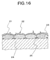
- the present inventors note that in the thin image display device such as the FED, many fine fragments of the metal back layer adhere to the cathode side due to the occurrence of abnormal discharge even when there is no projecting portion which triggers discharge on the surface of the metal back layer. As a result of investigating the phosphor screen of the image display device in which such discharge occurs, it is found that as shown in FIG. 16, innumerable minute projections 22 are formed on the surface of an Al film which is a metal back layer 21 and these projection 22 portions are about to peel off.
- the present invention has been made in view of these respects and its object is to provide a metal back-attached phosphor screen with excellent withstand voltage characteristics capable of increasing the electron beam accelerating voltage without causing the occurrence of abnormal discharge and being applied to a thin image display device with a high light-emission brightness.
- the present invention is obtained as a result of diligently repeating experiments on the correlation between the adhesive force between a phosphor layer and a metal back layer and the occurrence of electric discharge in a thin image display device such as a FED.
- a first aspect of the present invention is a metal back-attached phosphor screen comprising a phosphor layer and a metal back layer on an inner surface of a face plate, in which a first treatment layer containing an oxide of one kind or two or more kinds of elements selected from the group consisting of silicon, aluminum, titanium, and zirconium is formed on the phosphor layer and the metal back layer is formed on the first treatment layer.
- a second aspect of the present invention is a metal back-attached phosphor screen comprising a phosphor layer and a metal back layer on an inner surface of a face plate, in which a first treatment layer containing one kind or two or more kinds of inorganic oxides selected from the group consisting of silicon oxide, a silicon oxide containing one kind or two or more kinds of alkalimetal elements, aluminum oxide, titanium oxide, and zirconium oxide is formed on the phosphor layer and the metal back layer is formed on the first treatment layer.
- a third aspect of the present invention is a method of forming a metal back-attached phosphor screen which comprises forming a phosphor layer on an inner surface of a face plate, forming a first treatment layer containing an oxide of one kind or two or more kinds of elements selected from the group consisting of silicon, aluminum, titanium, and zirconium on the phosphor layer, and forming a metal back layer on the first treatment layer.
- a fourth aspect of the present invention is a method of forming a metal back-attached phosphor screen which comprises forming a phosphor layer on an inner surface of a face plate, forming a first treatment layer containing one kind or two or more kinds of inorganic oxides selected from the group consisting of silicon oxide, a silicon oxide containing one kind or two or more kinds of alkalimetal elements, aluminum oxide, titanium oxide, and zirconium oxide on the phosphor layer, and forming a metal back layer on the first treatment layer.
- a fifth aspect of the present invention is an image display device which comprises a face plate, a rear plate disposed facing the face plate, numerous electron emitting elements formed on the rear plate, and a phosphor screen formed on the face plate in such a way as to face the rear plate and emitting light by electron beams emitted from the electron emitting elements, the phosphor screen being the aforementioned metal back-attached phosphor screen in the present invention.
- FIG. 1 is a sectional view showing a first embodiment of a metal back-attached phosphor screen of the present invention.
- numeral 1 denotes a glass substrate of a face plate.
- a light absorption layer 2 in a predetermined pattern (for example, in a striped pattern) composed of a black pigment or the like is formed on an inner surface of the glass substrate 1 by photolithography or the like, and a phosphor layer 3 of three colors of blue (B), green (G) , and red (R) is formed on the pattern of the light absorption layer 2 by a slurry method using ZnS-based, Y 2 O 3 -based, and Y 2 O 2 S-based phosphor liquids or the like.
- the phosphor layer 3 of individual colors can also be formed by a spray method or a printing method. When the spray method or the printing method is used, patterning by photolithography can be used together, if necessary.
- the phosphor screen having the pattern of the light absorption layer 2 and the three-color pattern of the phosphor layer 3 is formed, as described above.
- a first treatment layer 4 containing an inorganic oxide is formed on this phosphor screen.
- the inorganic oxide silicon dioxide (SiO 2 ), a silicon oxide containing an alkali metal such as Na, K, or Li, aluminum oxide (Al 2 O 3 ), titanium oxide (TiO 2 ), zirconium oxide (ZrO 2 ), or the like is used.
- a method of applying/drying a colloidal silica solution or a Na silicate (sodium silicate) solution and heat-treating (baking) a resulting coating film can be adopted.
- a silica (SiO 2 ) particle layer is formed.
- an alkali silicate glass (Na 2 O • nSiO 2 ) layer is formed.
- a film containing at least one kind of oxide selected from SiO 2 , TiO 2 , and ZrO 2 can be formed by a sol-gel method.
- a liquid containing oligomer which is obtained by hydrolyzing and polycondensing alkoxide such as ethyl silicate or methyl silicate in a solution containing an organic solvent and heat-treating (baking) a coating film, a SiO 2 film can be formed.
- a metal back layer 5 made of a metal film such as an Al film is formed on the first treatment layer 4 containing the aforementioned inorganic oxide.
- the metal film of Al or the like can be vacuum-deposited on a thin film made of an organic resin such as nitrocellulose, for example, formed by a spin method, then be heat-treated (baked) at a temperature approximately between 400°C and 450°C, and an organic material can be decomposed/removed.
- the first treatment layer 4 containing the inorganic oxide such as silicon dioxide (SiO 2 ), a silicon oxide containing an alkali metal such as Na, K, or Li, aluminum oxide (Al 2 O 3 ), titanium oxide (TiO 2 ), or zirconium oxide (ZrO 2 ) is disposed on the phosphor layer 3, and the metal back layer 5 is formed on the first treatment layer 4, whereby adhesive strength between the metal back layer 5 and a layer thereunder is large, and the metal layer 5 is resistant to peeling even when an electric field is applied. Accordingly, the probability of occurrence of abnormal discharge is low, resulting in excellent withstand voltage characteristics.
- a second treatment layer 6 is formed on the metal back layer 5.
- the structures of the other portions are the same as those in the first embodiment, and hence an explanation thereof is omitted.
- the second treatment layer 6 As a material composing the second treatment layer 6, an inorganic oxide of the same kind as the first treatment layer 4 can be used.
- the second treatment layer 6 can be formed in the same manner as in forming the first treatment layer 4.
- the first treatment layer 4 containing the inorganic oxide such as silicon dioxide (SiO 2 ), titanium oxide (TiO 2 ), or zirconium oxide (ZrO 2 ) is formed on the phosphor layer 3, and besides the second treatment layer 6 containing the aforementioned inorganic oxide is also formed on the metal back layer 5, whereby the adhesive strength of the metal back layer 5 is further improved. Accordingly, the metal back layer 5 becomes more resistant to peeling, which prevents the occurrence of abnormal discharge.
- the inorganic oxide such as silicon dioxide (SiO 2 ), titanium oxide (TiO 2 ), or zirconium oxide (ZrO 2 )
- the adhesive force of the metal back layer 5 is increased, which can efficiently improve withstand voltage characteristics.
- the first treatment layer can be formed through a two-step coating film formation process as shown below.
- an upper coating film can be formed on the lower coating film by applying/drying a coating solution which contains water such as a colloidal silica solution or a Na silicate solution.
- a coating solution which contains an organic solvent such as a mixed solution containing oligomer which is obtained by hydrolyzing and polycondensing alkoxide such as Si alkoxide.
- the treatment layer made of the inorganic oxide is formed. This makes it possible to inhibit deterioration of a phosphor due to adhesion of the organic solvent and prevent reduction in brightness.
- FIG. 3 a FED including the metal-baked phosphor screen as an anode electrode is shown in FIG. 3.
- a face plate 7 having a metal back-attached phosphor screen M in the aforementioned first embodiment and a rear plate 9 having electron emitting elements 8 arranged in a matrix are placed facing to each other with a space as narrow as approximately from one millimeter to several millimeters, and a high voltage from 5 kV to 15 kV is applied between the face plate 7 and the rear plate 9.
- Numeral 10 in this figure denotes a supporting frame (sidewall).
- the space between the face plate 7 and the rear plate 9 is extremely narrow and discharge (dielectric breakdown) tends to occur between these plates, but in the FED, the metal back layer is resistant to peeling since its adhesive strength is large, whereby the probability of production of projecting portions which trigger discharge is low. Hence, the occurrence of discharge is inhibited, and thereby withstand voltage characteristics are greatly improved.
- the first treatment layer containing one kind or two or more kinds of inorganic oxides selected from silicon oxide, a silicon oxide containing one kind or two or more kinds of alkalimetal elements, aluminum oxide, titanium oxide, and zirconium oxide is formed on the phosphor layer, and the metal back layer is formed on the first treatment layer, whereby the adhesion strength between the layer containing the aforementioned inorganic oxide and the metal back layer is large, and therefore the metal back layer is resistant to peeling caused by the application of voltage. Accordingly, excellent withstand voltage characteristics are attained, and the probability of occurrence of abnormal discharge is low. Moreover, the electron beam accelerating voltage can be increased, and hence an image display device with high light-emission brightness can be obtained.
- a coating film was formed on the phosphor layer by coating a solution of colloidal silica whose solid content concentration was adjusted and a solution of Na silicate whose solid content concentrationwas also adjusted, and the correlation between adhesive force between the phosphor layer and the metal-back layer and discharge occurrence was examined.
- the procedure for fabricating samples is shown below.
- blue phosphor layers were formed on soda glass substrates (10 cm long X 10 cm wide) by the slurry method.
- colloidal silica solutions whose solid content concentrations were adjusted to 2%, 5%, 10%, and 20%, respectively by dilution with pure water, and Na silicate (water glass) solutions whose concentrations were adjusted similarly were applied onto the aforementioned phosphor layers by the spray method to form coating films. Additionally, a sample in which the coating film was not formed on the phosphor layer was prepared.
- the coating film formed of the colloidal silica solution finally becomes a layer including silica (SiO 2 ) particles by baking.
- the coating film formed of the Na silicate solution becomes a layer including alkali silicate glass (Na 2 O • nSiO 2 ) particles.
- the adhesive force of the metal back layers was evaluated in the way shown below.
- three kinds of adhesive sheets different in adhesion were fabricated by applying/drying toluene solutions of vinyl acetate (solid content concentrations 1%, 2%, and 4%) on a polyethylene film 20 ⁇ m in thickness using a bar coater.
- FIG. 4 shows the relation between the solid content concentration of the colloidal silica solution and the adhesive force evaluation score
- FIG. 5 shows the relation between the solid content concentration of the Na silicate (water glass) solution and the adhesive force evaluation score.
- the metal back-attached phosphor screen sample fabricated by the aforementioned method and a substrate obtained by forming an ITO film on a soda glass plate by deposition were placed in such a way that a surface on which ITO was deposited faced the metal-baked phosphor screen and a gap therebetween was maintained at 2 mm.
- a pseudo electron beam accelerator was fabricated by connecting the metal back-attached phosphor screen as an anode and the ITO film as a cathode to a direct current power supply in an atmosphere which was a vacuum of approximately 1 ⁇ 10 -5 Pa.
- FIG. 6 shows the relation between the solid content concentration of the colloidal silica solution and the critical holding voltage
- FIG. 7 shows the relation between the solid content concentration of the Na silicate solution and the critical holding voltage.
- Colloidal silica solutions whose solid content concentrations were adjusted to 2%, 5%, 10%, and 20%, respectively, by dilution with pure water, and Na silicate solutions whose concentrations were adjusted similarly were applied onto the metal back layers (Al films) of the respective samples fabricated in Example 1 by the spray method to form coating films. Thereafter, the second treatment layer composed of the inorganic oxide was formed on each of the metal back layers by baking at 430°C for 30 minutes.
- the curve b in FIG. 4 and the curve b in FIG. 6 show measurement results when the first treatment layer is formed on the phosphor layer by using the colloidal silica solution and the second treatment layer is formed on the Al film by using the colloidal silica solution whose solid content concentration is 2%, and similarly the curves c, the curves d, and the curves e in FIG. 4 and FIG. 6 respectively show measurement results when the coating solution on the phosphor layer is the colloidal silica solution and the coating solutions on the Al film are 5%, 10%, and 20% colloidal silica solutions.
- the curve b in FIG. 5 and the curve b in FIG. 7 show measurement results when the first treatment layer is formed on the phosphor layer by using the Na silicate solution and the second treatment layer is formed on the Al film by using the Na silicate solution whose solid content concentration is 2%, and similarly the curves c, the curves d, and the curves e in FIG. 5 and FIG. 7 respectively show measurement results when the coating solution on the phosphor layer is the Na silicate solution and the coating solutions on the Al film are 5%, 10%, and 20% Na silicate solutions.
- the curve a in FIG. 8 shows a measurement result when the solution applied onto the phosphor layer is the colloidal silica solution and no coating treatment is performed on the Al film
- the curve b, the curve c, the curve d, and the curve e in FIG. 8 show measurement results when the coating solution on the phosphor layer is the colloidal silica solution and the solutions applied onto the Al film are colloidal silica solutions whose solid content concentrations are 2%, 5%, 10%, and 20%, respectively.
- the curve a in FIG. 9 shows a measurement result when the solution applied onto the phosphor layer is the Na silicate solution and no coating treatment is performed on the Al film
- the curve b, the curve c, the curve d, and the curve e in FIG. 9 show measurement results when the coating solution on the phosphor layer is the Na silicate solution and the solutions applied onto the Al film are Na silicate solutions whose solid content concentrations are 2%, 5%, 10%, and 20%, respectively.
- the driving voltage anode voltage
- the driving voltage was changed in a range from 5 kV to 15 kV
- Respective curves in FIG. 10 show measurement results when the anode voltage is 5 kV, 7 kV, 10kV, and 15 kV.
- the lower the driving voltage the sharper peak appears in the light-emission brightness, and the peak value appears when the thickness of the Al film is approximately 50 nm.
- the driving voltage is less than 3 kV in approximately 50 nm of the Al film thickness, the electron beam does not easily pass through the metal back layer, and therefore the phosphor hardly emits light. Accordingly, it turns out that the metal back-attached phosphor screen cannot be used as a phosphor screen unless the critical holding voltage is equal to or higher than 3 kV.
- the solid content concentration of the colloidal silica solution or the Na silicate solution as the coating solution and the content of the inorganic oxide in the first or the second treatment layer formed from this coating solution are in proportion. Hence, an optimum range of the content of the inorganic oxide in the first or the second treatment layer can be found from an optimum range of the aforementioned solid content concentration of the coating solution.
- an adhesive tape was stuck on an Al film side of the sample by pressing it with a finger. Then, the adhesive tape was stripped off and separated into a layer lower than the Al film (decomposition sample-1) and a layer including and upper than the Al film (decomposition sample-2). Subsequently, both the samples were decomposed by an acid and subjected to elemental analysis by an ICP-AES method.
- the weight per unit area of the phosphor was found by the following method. First, after the weight of Zn which was a basic component of the used blue phosphor was found, the weight was converted into ZnS to obtain the weight of the phosphor. Then, after the weight of the Si being a component of the first treatment layer was found, the weight was converted into SiO 2 to obtain the weight of the first treatment layer.
- the metal back-attached phosphor screen having a critical holding voltage equal to or higher than 3 kV could be obtained and used as a phosphor screen of a thin display device.
- a mixed solution containing oligomer which was obtained by hydrolyzing and polycondensing various kinds of alkoxides was prepared in the way shown below. At least one kind selected from tetraethyl silicate (tetraethoxysilane), tetraethyl titanate (tetraethoxytitanium), and zirconium tetra-n-butoxide was used as the alkoxide, and the hydrolysis was performed stepwise according to the number of used alkoxides to prepare the coating solution in which oligomer was mixed.
- tetraethyl silicate tetraethoxysilane
- tetraethyl titanate tetraethoxytitanium
- zirconium tetra-n-butoxide zirconium tetra-n-butoxide
- IPA isopropyl alcohol
- the mixed solution containing two or more kinds of oligomers prepared through the aforementioned procedure was used in place of the colloidal silica solution and the Na silicate solution to form the coating film on the phosphor layer by the spray method. Then, after an organic film was formed on the coating film by the well-known lacquer method, Al was deposited on the organic film by a deposition method to form an Al film 100 nm in thickness, and thereafter, organic components were decomposed/removed by baking at 430°C for 30 minutes. Moreover, after a coating film was also formed on the Al film thus formed using the aforementioned mixed solution, the coating film was baked.
- composite oxide layers containing a SiO 2 component, a TiO 2 component, and a ZrO 2 component in various percentages (weight ratios) were formed on the phosphor layer and the Al film.
- the solid content concentration and the coating thickness of the mixed solution were adjusted in such a way that the content per unit area of all the inorganic oxides finally formed by heat treatment was 10% of the content of the phosphor of the lower layer.
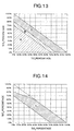
- FIG. 11 shows the adhesive force with respect to the percentages of SiO 2 and TiO 2 , and the remaining percentage is the percentage of ZrO 2 .
- a region A shows a region where the adhesive force scores less than 8 points and is the same as that when colloidal silica, Na silicate, or the like is used singly
- a region B shows a region where the adhesive force scores 8 points to 10 points and is slightly improved
- a region C shows a region where the adhesive force gets full 12 points, respectively.
- the adhesive force improves. If approximate numerical expressions are formulated, it is said that the adhesive force further improves in a region where all the following expressions hold when SiO 2 is x%, TiO 2 is y%, and ZrO 2 is z%.
- x + y ⁇ 100 x + 0.5y ⁇ 80 x + y + z 100 (where x > 0, y > 0, z > 0)
- the critical holding voltage in the region A was less than 6 kV
- the critical holding voltage in the region B was 6 kV to 9 kV
- the critical holding voltage in the region C was 9 kV to 12 kV.
- FIG. 12 The schematic structure of a brightness measuring device is shown in FIG. 12.
- numeral 11 denotes a vacuum chamber which is also used as an earth to house the sample
- numeral 12 denotes a vacuum pump
- numeral 13 denotes a lid to take out the sample
- numeral 14 denotes a brightness measuring glass window
- numeral 15 denotes a deflection yoke
- numeral 16 denotes an electron gun for the CRT
- numeral 17 denotes an electron gun atmosphere interrupting unit
- numeral 18 denotes an anode supply terminal, respectively.
- the sample was placed in the vacuum chamber with its metal back layer facing toward the electron gun side, and the metal back layer and an anode terminal were connected.
- the space between the electron gun and the sample was set to 30 cm in order to prevent discharge caused by the deposition of the metal back layer.
- the interior of the vacuum chamber was maintained at a vacuum of approximately 1 ⁇ 10 -5 Pa, the electron gun and the deflection yoke were driven at a des ired anode voltage, and the brightness was measured from the brightness measuring glass window. Measurement results are shown in FIG. 13.
- FIG. 13 shows the distribution of brightness reduction rate with respect to the percentages of SiO 2 and TiO 2 (at an anode voltage of 5 kV), and the remaining percentage is the percentage of ZrO 2 .
- a region A shows a region of no practical use where the brightness reduction rate is equal to or more than 30%
- a region B is a practical-level region where the brightness reduction rate is equal to or more than 10% and less than 30%
- a region C is a region where the brightness reduction rate is less than 10% and the brightness is specially satisfactory, respectively.
- the compounding ratio needs to be determined in a combined region of the aforementioned respective regions in order to efficiently utilize the property of high adhesive force of a composite metal oxide film containing three components of Si, Ti, and Zr in a practical-level region of brightness. This is shown by a region A 0 in FIG. 14.
- the critical holding voltage reached 20 kV at the maximum in some samples.
- SiO 2 • TiO 2 compounded type oxide an oxide in which the SiO 2 component and the TiO 2 component were bonded in a matrix in a predetermined ratio (hereinafter referred to as a SiO 2 • TiO 2 compounded type oxide) which was obtained by hydrolyzing and polycondensing (copolymerizing) silicon alkoxide and titanium alkoxide by the sol-gel method was provided on the phosphor layer, adhesive force and withstand voltage characteristic were improved.
- the SiO 2 • ZrO 2 compounded type oxide was provided on the phosphor layer, the adhesive force of the metal back layer and the withstand voltage characteristics were still further improved.
- FIG. 15 is a graph showing the relation between the adhesive force of the metal back layer and the brightness reduction obtained as a result of measurement.
- a curve f in this figure shows brightness degradation when the colloidal silica solution or the Na silica solution is applied. In any combination, almost the same result can be obtained. It is known that the brightness degradation hardly occurs until the adhes ive force saturation concentration is reached, and there is practically no problem if coating is performed at a saturation point of adhesive force.
- a curve g shows brightness degradation when the solution in the ratio of 20% SiO 2 , 70% TiO 2 and 10% ZrO 2 is applied
- a curve h shows brightness degradation when the solution in the ratio of 15% SiO 2 , 60% TiO 2 and 25% ZrO 2 is applied.
- the solution in the ratio of 20% SiO 2 , 70% TiO 2 and 10% ZrO 2 and the solution in the ratio of 15% SiO 2 , 60% TiO 2 and 25% ZrO 2 were prepared while their concentrations were varied and the solutions with various adhesive forces were applied.
- the brightness when the solution in the ratio of 20% SiO 2 , 70% TiO 2 and 10% ZrO 2 was applied was as shown by a curve i.
- the brightness when the solution in the ratio of 15% SiO 2 , 60% TiO 2 and 25% ZrO 2 was applied was as shown by a curve j, and hence in each case, brightness degradation was inhibited.
- the degree of reduction in light-emission brightness with respect to the degree of increase in the adhesive force of the metal-back layer is high.
- the degree of reduction in brightness with respect to the degree of increase in adhesive force is low.
- the reduction in light-emission brightness is small, and particularly the sample in which the SiO 2 • TiO 2 compounded type oxide layer is formed has excellent brightness characteristics. Moreover, in the sample having the SiO 2 • ZrO 2 compounded type oxide layer, the adhesive force of the metal back layer is greatly improved.
- a phosphor screen whose metal back layer has a high adhesive strength and is resistant to peeling caused by voltage application can be obtained. Accordingly, the electron beam accelerating voltage can be increased because of excellent withstand voltage characteristics and a low probability of occurrence of abnormal discharge, and a high-voltage drive and high light-emission brightness thin display device can be realized.
Landscapes
- Engineering & Computer Science (AREA)
- Manufacturing & Machinery (AREA)
- Cathode-Ray Tubes And Fluorescent Screens For Display (AREA)
- Luminescent Compositions (AREA)
- Formation Of Various Coating Films On Cathode Ray Tubes And Lamps (AREA)
Applications Claiming Priority (3)
| Application Number | Priority Date | Filing Date | Title |
|---|---|---|---|
| JP2002314467A JP2004152538A (ja) | 2002-10-29 | 2002-10-29 | メタルバック付き蛍光面とその形成方法および画像表示装置 |
| JP2002314467 | 2002-10-29 | ||
| PCT/JP2003/013823 WO2004040613A1 (ja) | 2002-10-29 | 2003-10-29 | メタルバック付き蛍光面とその形成方法および画像表示装置 |
Publications (1)
| Publication Number | Publication Date |
|---|---|
| EP1560249A1 true EP1560249A1 (de) | 2005-08-03 |
Family
ID=32211614
Family Applications (1)
| Application Number | Title | Priority Date | Filing Date |
|---|---|---|---|
| EP03769936A Withdrawn EP1560249A1 (de) | 2002-10-29 | 2003-10-29 | Leuchtstoffschirm mit metallrückseite, zugehöriges herstellungsverfahren und bildanzeigeeinheit |
Country Status (7)
| Country | Link |
|---|---|
| US (1) | US20060125372A1 (de) |
| EP (1) | EP1560249A1 (de) |
| JP (1) | JP2004152538A (de) |
| KR (1) | KR100732572B1 (de) |
| CN (1) | CN1708824A (de) |
| TW (1) | TW200410281A (de) |
| WO (1) | WO2004040613A1 (de) |
Families Citing this family (9)
| Publication number | Priority date | Publication date | Assignee | Title |
|---|---|---|---|---|
| JP2004303682A (ja) * | 2003-04-01 | 2004-10-28 | Toshiba Corp | メタルバック付き蛍光面の形成方法 |
| JP4015102B2 (ja) * | 2003-11-21 | 2007-11-28 | 株式会社東芝 | メタルバック付き蛍光面の形成方法 |
| EP3012872B1 (de) | 2004-05-21 | 2017-07-12 | Hitachi Metals, Ltd. | Solarzelle |
| KR20050113900A (ko) * | 2004-05-31 | 2005-12-05 | 삼성에스디아이 주식회사 | 전자 방출 소자 및 이의 제조 방법 |
| JP2006019219A (ja) * | 2004-07-05 | 2006-01-19 | Toshiba Corp | 表示装置 |
| JP2008004280A (ja) * | 2006-06-20 | 2008-01-10 | Sony Corp | 平面型表示装置 |
| EP2036111B1 (de) * | 2006-06-28 | 2013-04-24 | Thomson Licensing | Leuchtanzeigeanordnung mit füllermaterial |
| JP2012235059A (ja) * | 2011-05-09 | 2012-11-29 | Toshiba Corp | 半導体装置および半導体装置の製造方法 |
| CN111243922B (zh) * | 2020-01-16 | 2022-11-18 | 中国建筑材料科学研究总院有限公司 | 荧光薄膜屏、其制备方法及其在微通道板像增强器的应用 |
Family Cites Families (11)
| Publication number | Priority date | Publication date | Assignee | Title |
|---|---|---|---|---|
| JPS54105959A (en) * | 1978-02-08 | 1979-08-20 | Hitachi Ltd | Manufacture of color picture tube |
| US20030034726A1 (en) * | 1998-11-13 | 2003-02-20 | Kimiyo Ibaraki | Color cathode -ray tube and method of manufacturing the same |
| JP2000319588A (ja) * | 1999-05-10 | 2000-11-21 | Sony Corp | 熱吸収膜用塗料、熱吸収膜およびカラー陰極線管 |
| KR100460468B1 (ko) * | 2000-02-03 | 2004-12-08 | 후지시끼소 가부시끼 가이샤 | 전사 필름, 메탈백층 형성 방법 및 화상 표시 장치 |
| JP2002075239A (ja) * | 2000-08-25 | 2002-03-15 | Toshiba Corp | カラー陰極線管とその製造方法および蒸着用複合材料 |
| JP2002141000A (ja) * | 2000-10-31 | 2002-05-17 | Toshiba Corp | メタルバック付き蛍光体層とその形成方法および画像表示装置 |
| US6812636B2 (en) * | 2001-03-30 | 2004-11-02 | Candescent Technologies Corporation | Light-emitting device having light-emissive particles partially coated with light-reflective or/and getter material |
| JP2002343241A (ja) * | 2001-05-10 | 2002-11-29 | Toshiba Corp | メタルバック付き蛍光面の形成方法および画像表示装置 |
| JP2002343248A (ja) * | 2001-05-10 | 2002-11-29 | Toshiba Corp | 蛍光面の形成方法および画像表示装置 |
| JP2003031150A (ja) * | 2001-07-13 | 2003-01-31 | Toshiba Corp | メタルバック付き蛍光面、メタルバック形成用転写フィルムおよび画像表示装置 |
| JP3848202B2 (ja) * | 2002-04-19 | 2006-11-22 | キヤノン株式会社 | 蛍光面基板の製造方法 |
-
2002
- 2002-10-29 JP JP2002314467A patent/JP2004152538A/ja not_active Abandoned
-
2003
- 2003-10-29 WO PCT/JP2003/013823 patent/WO2004040613A1/ja not_active Ceased
- 2003-10-29 TW TW092130114A patent/TW200410281A/zh unknown
- 2003-10-29 US US10/532,980 patent/US20060125372A1/en not_active Abandoned
- 2003-10-29 KR KR1020057007108A patent/KR100732572B1/ko not_active Expired - Fee Related
- 2003-10-29 CN CNA2003801021471A patent/CN1708824A/zh active Pending
- 2003-10-29 EP EP03769936A patent/EP1560249A1/de not_active Withdrawn
Non-Patent Citations (1)
| Title |
|---|
| See references of WO2004040613A1 * |
Also Published As
| Publication number | Publication date |
|---|---|
| CN1708824A (zh) | 2005-12-14 |
| JP2004152538A (ja) | 2004-05-27 |
| KR100732572B1 (ko) | 2007-06-27 |
| KR20050059296A (ko) | 2005-06-17 |
| WO2004040613A1 (ja) | 2004-05-13 |
| TW200410281A (en) | 2004-06-16 |
| US20060125372A1 (en) | 2006-06-15 |
Similar Documents
| Publication | Publication Date | Title |
|---|---|---|
| EP1030339B1 (de) | Lumineszenzmittel, pulverförmiges lumineszenzmittel, plasma-anzeigetafel und herstellungsverfahren dersleben | |
| US6160345A (en) | Plasma display panel with metal oxide layer on electrode | |
| JP3234526B2 (ja) | プラズマディスプレイパネルおよびプラズマディスプレイ用蛍光体の製造方法 | |
| EP1255276B1 (de) | Plasmaanzeigetafel und Verfahren zu ihrer Herstellung | |
| US20060125372A1 (en) | Phosphor screen with metal back, method of forming the same and image display unit | |
| JP2003082345A (ja) | プラズマディスプレイ装置 | |
| US20040075375A1 (en) | Plasma display panel and its manufacturing method | |
| US8004171B2 (en) | Dielectric layer containing carbon for a plasma display panel | |
| EP2194561A2 (de) | Lichtemissionsvorrichtung und die Lichtemissionsvorrichtung als Lichtquelle nutzende Anzeigevorrichtung | |
| KR100813241B1 (ko) | 전계방출형 백라이트 유니트 및 그 상부패널의 제조방법 | |
| JP4519610B2 (ja) | プラズマディスプレイパネル用保護膜形成用塗布液 | |
| JP2007109410A (ja) | プラズマディスプレイパネルの製造方法、および、プラズマディスプレイパネル | |
| JP3621225B2 (ja) | 発光表示デバイス | |
| JP2006139999A (ja) | プラズマディスプレイパネル用保護膜およびその形成方法並びにプラズマディスプレイパネル | |
| KR100361450B1 (ko) | 교류형 플라즈마디스플레이패널용 보호막재료 | |
| EP1506988A1 (de) | Plasma-bildschirmgerät | |
| JPH11329254A (ja) | プラズマディスプレイパネル | |
| JP2004214049A (ja) | ガス放電パネルおよびその製造方法 | |
| JP2004220929A (ja) | ガス放電パネルおよびその製造方法 | |
| JP2003031113A (ja) | メタルバック付き蛍光面と画像表示装置およびメタルバック付き蛍光面の形成方法 | |
| US20080129186A1 (en) | Image display device and spacer | |
| CN101652449A (zh) | 发光显示装置、等离子体显示装置和荧光体粒子 | |
| JP2005050640A (ja) | 投射型陰極線管用パネルガラスおよび投射型陰極線管 | |
| JP2002100308A (ja) | 陰極線管 | |
| KR20020069048A (ko) | 프로젝션 텔레비젼용 음극선관 |
Legal Events
| Date | Code | Title | Description |
|---|---|---|---|
| PUAI | Public reference made under article 153(3) epc to a published international application that has entered the european phase |
Free format text: ORIGINAL CODE: 0009012 |
|
| 17P | Request for examination filed |
Effective date: 20050512 |
|
| AK | Designated contracting states |
Kind code of ref document: A1 Designated state(s): AT BE BG CH CY CZ DE DK EE ES FI FR GB GR HU IE IT LI LU MC NL PT RO SE SI SK TR |
|
| RBV | Designated contracting states (corrected) |
Designated state(s): DE FR GB IT NL |
|
| STAA | Information on the status of an ep patent application or granted ep patent |
Free format text: STATUS: THE APPLICATION HAS BEEN WITHDRAWN |
|
| 18W | Application withdrawn |
Effective date: 20080219 |