EP1559136B1 - Verfahren zum schnellen tempern von mehrschicht-wafern mit einer kante - Google Patents
Verfahren zum schnellen tempern von mehrschicht-wafern mit einer kante Download PDFInfo
- Publication number
- EP1559136B1 EP1559136B1 EP03772490A EP03772490A EP1559136B1 EP 1559136 B1 EP1559136 B1 EP 1559136B1 EP 03772490 A EP03772490 A EP 03772490A EP 03772490 A EP03772490 A EP 03772490A EP 1559136 B1 EP1559136 B1 EP 1559136B1
- Authority
- EP
- European Patent Office
- Prior art keywords
- wafer
- annealing
- peripheral region
- edge
- thermal
- Prior art date
- Legal status (The legal status is an assumption and is not a legal conclusion. Google has not performed a legal analysis and makes no representation as to the accuracy of the status listed.)
- Expired - Lifetime
Links
Images

Classifications
-
- H—ELECTRICITY
- H10—SEMICONDUCTOR DEVICES; ELECTRIC SOLID-STATE DEVICES NOT OTHERWISE PROVIDED FOR
- H10P—GENERIC PROCESSES OR APPARATUS FOR THE MANUFACTURE OR TREATMENT OF DEVICES COVERED BY CLASS H10
- H10P95/00—Generic processes or apparatus for manufacture or treatments not covered by the other groups of this subclass
- H10P95/90—Thermal treatments, e.g. annealing or sintering
-
- H—ELECTRICITY
- H10—SEMICONDUCTOR DEVICES; ELECTRIC SOLID-STATE DEVICES NOT OTHERWISE PROVIDED FOR
- H10P—GENERIC PROCESSES OR APPARATUS FOR THE MANUFACTURE OR TREATMENT OF DEVICES COVERED BY CLASS H10
- H10P95/00—Generic processes or apparatus for manufacture or treatments not covered by the other groups of this subclass
- H10P95/90—Thermal treatments, e.g. annealing or sintering
- H10P95/906—Thermal treatments, e.g. annealing or sintering for altering the shape of semiconductors, e.g. smoothing the surface
-
- H—ELECTRICITY
- H10—SEMICONDUCTOR DEVICES; ELECTRIC SOLID-STATE DEVICES NOT OTHERWISE PROVIDED FOR
- H10P—GENERIC PROCESSES OR APPARATUS FOR THE MANUFACTURE OR TREATMENT OF DEVICES COVERED BY CLASS H10
- H10P72/00—Handling or holding of wafers, substrates or devices during manufacture or treatment thereof
- H10P72/04—Apparatus for manufacture or treatment
- H10P72/0431—Apparatus for thermal treatment
- H10P72/0432—Apparatus for thermal treatment mainly by conduction
-
- H—ELECTRICITY
- H10—SEMICONDUCTOR DEVICES; ELECTRIC SOLID-STATE DEVICES NOT OTHERWISE PROVIDED FOR
- H10P—GENERIC PROCESSES OR APPARATUS FOR THE MANUFACTURE OR TREATMENT OF DEVICES COVERED BY CLASS H10
- H10P90/00—Preparation of wafers not covered by a single main group of this subclass, e.g. wafer reinforcement
- H10P90/19—Preparing inhomogeneous wafers
- H10P90/1904—Preparing vertically inhomogeneous wafers
- H10P90/1906—Preparing SOI wafers
- H10P90/1914—Preparing SOI wafers using bonding
-
- H—ELECTRICITY
- H10—SEMICONDUCTOR DEVICES; ELECTRIC SOLID-STATE DEVICES NOT OTHERWISE PROVIDED FOR
- H10P—GENERIC PROCESSES OR APPARATUS FOR THE MANUFACTURE OR TREATMENT OF DEVICES COVERED BY CLASS H10
- H10P90/00—Preparation of wafers not covered by a single main group of this subclass, e.g. wafer reinforcement
- H10P90/19—Preparing inhomogeneous wafers
- H10P90/1904—Preparing vertically inhomogeneous wafers
- H10P90/1906—Preparing SOI wafers
- H10P90/1914—Preparing SOI wafers using bonding
- H10P90/1916—Preparing SOI wafers using bonding with separation or delamination along an ion implanted layer, e.g. Smart-cut
-
- H—ELECTRICITY
- H10—SEMICONDUCTOR DEVICES; ELECTRIC SOLID-STATE DEVICES NOT OTHERWISE PROVIDED FOR
- H10W—GENERIC PACKAGES, INTERCONNECTIONS, CONNECTORS OR OTHER CONSTRUCTIONAL DETAILS OF DEVICES COVERED BY CLASS H10
- H10W10/00—Isolation regions in semiconductor bodies between components of integrated devices
- H10W10/10—Isolation regions comprising dielectric materials
- H10W10/181—Semiconductor-on-insulator [SOI] isolation regions, e.g. buried oxide regions of SOI wafers
Definitions
- the present invention relates to a method of applying heat treatment to a multilayer wafer with an edge, the wafer being made of materials selected from semiconductive materials.
- multilayer wafer with an edge is used herein to mean a wafer of semiconductive material which presents the following two characteristics:
- SOI silicon on insulator
- FIG. 1 This is shown in highly diagrammatic manner in Figure 1 , in which there can be seen a wafer 10 of SOI after detachment, the wafer comprising a support layer 100, an insulating layer 101, and a working layer 102 of silicon, the layers 101 and 102 defining a peripheral edge 1020 that is a few millimeters wide.
- SOI constitutes only one of the applications of the invention, and it is used merely by way of illustration in the present text.
- the invention is applicable to any type of multilayer wafer with an edge that is made of materials selected from semiconductive materials.
- Such wafers are generally subjected to heat treatments, e.g. for the purposes of modifying the composition of one or more layers of the wafer, of stabilizing a bonding interface between two layers, of curing structural defects, and/or of improving the surface state of the wafer, ....
- Such heat treatments can be implemented in a wide variety of manners.
- low temperatures are defined by convention as being less than a value of about 500°C to 600°C.
- Annealing may also be undertaken at "high" temperatures, i.e. at values greater than about 500°C-600°C.
- RTP rapid thermal processing
- the processing temperature is generally very high (typically about 950°C or higher), and the annealing time is kept down to a duration of the order of a few minutes.
- the effect of such annealing is to smooth the surface of a wafer.
- Wafers in particular SOI wafers can also be subjected to other types of RTP annealing, for example annealing of the rapid thermal oxidation (RTO) type.
- RTP annealing which is performed under an oxidizing atmosphere, serves to oxidize the surface of the wafer.
- the wafers to which the invention applies can thus be subjected to various types annealing.
- slip lines are generated in particular by temperature non-uniformities in three dimensions within an annealing furnace (i.e. temperature is not strictly identical at all points), and they develop under the effect of the above-mentioned very high levels of thermal stress.
- slip lines are generally initiated in the peripheral region of the wafer.
- RTP type annealing thus tends to generate slip lines, and this drawback is more particularly severe in wafers concerned by the invention (multilayer wafers with an edge and made of materials selected from semiconductive materials).
- Such deformation is typically associated with wafers bending or twisting to some extent, as can be observed, for example by variation in the warp of the wafer.
- Warp represents the maximum deformation of the wafer relative to an "ideal" wafer, which should be absolutely flat.
- Such warp can also be observed with annealing performed in RTP mode.
- the object of the invention is to obviate these drawbacks.
- the invention provides a method of heat treating a multilayer wafer as defined in claim 1.
- Such a method relates specifically to the problem of multilayer wafers that have an edge. This problem which has been shown up by the Applicant is associated with differences of heat absorption coefficient at the edge of such a multilayer wafer.
- the invention also proposes the use of a method in accordance with any one of the above features in thermally processing an SOI wafer.
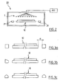
- an annealing installation 20 is shown for performing annealing on a wafer 10 with an edge.
- This installation is suitable for performing RTP type annealing, e.g. annealing for smoothing purposes.
- a particularly advantageous application of the invention thus lies with RTP type annealing, e.g. RTO annealing, or RTA type finishing annealing for smoothing the surface of the wafer.
- RTP type annealing e.g. RTO annealing
- RTA type finishing annealing for smoothing the surface of the wafer.
- the invention is not limited to this type of annealing, but applies to all of the modes of annealing mentioned in the introduction to this text.
- the installation 20 can thus be used to perform high-temperature annealing which does not constitute an RTP mode, or even low-temperature annealing.
- the wafer 10 is shown with only two visible layers. Nevertheless, the wafer may be any type of wafer, as mentioned above.
- the wafer 10 is an SOI wafer.
- the wafer being made of materials selected from semiconductive materials.
- it can be a wafer of silicon germanium on insulator (SGOI) or a wafer having a fine layer of SiGe on a supporting substrate (which may be of any kind, for example of Si), wafers of this category generally being associated with the same thermal stresses at the edge as are SOI wafers, which are used by way of example in the text below.
- SGOI silicon germanium on insulator
- SiGe silicon germanium on insulator
- the wafer may also be a multilayer wafer of the SOQ type (silicon on quartz).
- the wafers to which the invention applies are multilayer wafers including an edge, for which the invention provides an advantageous solution concerning any differences in heat absorption by the edge.
- the wafer 10 is heated by means of infrared lamps L which are disposed facing the wafer.
- a unit 200 serves to control electrical power supply to the lamps.
- the unit 200 is suitable for controlling the supply of power to the various lamps selectively and individually so as to control the power emitted individually by each of the lamps.
- thermal continuity structure 21 which surrounds the wafer 10, and which is spaced apart therefrom.
- the structure 21 is thus in the form of a closed ring which is placed concentrically about the wafer 10.
- edge ring serves to establish a certain amount of continuity in heat absorption beyond the edges of the wafer 10.
- edge ring 17 An example of such an edge ring is to be found in document WO 01/69656 (edge ring 17).
- edge rings In the prior art, the function of edge rings is limited to establishing a degree of thermal continuity in absorption beyond the borders of the wafer.
- edge rings are generally of a "basic" section that is rectangular in shape.
- edge rings improvements are proposed for such edge rings in order to perform a specific function of local and selective adaptation of heating at the peripheral edge of the wafer placed at the center of the edge ring.
- the spacing between the edge ring and the wafer it surrounds is generally dimensioned solely for the purpose of allowing the wafer to expand during the thermal processing.
- this spacing can be adapted selectively as a function of the thermal absorption coefficient at the edge of the wafer for the purpose of returning a greater or smaller amount of heat to the wafer (returning more heat when the spacing between the edge ring and the wafer is smaller).
- the lamps L facing said ring are powered selectively so as to adapt the heat power they radiate to the intrinsic heat absorption characteristics of said edge.
- the apparatus 20 is filled with a gaseous mixture, for example a mixture of hydrogen and argon, or it could be filled with pure argon.
- a gaseous mixture for example a mixture of hydrogen and argon, or it could be filled with pure argon.
- the wafer is heated for the most part by the direct infrared radiation coming from the lamps L, however a smaller part of its heating comes from thermal conduction via the gaseous mixture.
- Figure 4 thus represents the simple case of a wafer comprising a layer of silicon on a layer of oxide on a silicon substrate.
- the power supply to the lamps of the apparatus is adapted selectively to heat the central region to a greater or lesser extent than the peripheral region as a function of the heat absorption coefficients of these two regions:
- Determining the heat absorption coefficients of the layers of the multilayer wafer thus makes it possible to adapt the heating applied to the various regions of the multilayer wafer.
- heating can be adapted by other means, either as an alternative or in combination with such selective power supply to the heater means.
- the heat absorption coefficients can be determined in particular by using charts of the type shown in Figure 4 , which, for a multilayer wafer, plot the heat absorption coefficient as a function of the nature of the materials of the wafers and as a function of their thicknesses.
- use of the structure is optional: it can be omitted.
- thermal continuity structure can be adapted and implemented astutely to constitute second means for making the amount of heat actually absorbed by the various regions of the wafer more uniform.
- This second implementation can be optionally be combined with the first implementation.
- this structure can be placed around the wafer and at the same height as the wafer, as shown in Figure 2 .
- this thermal continuity structure may alternatively be placed around the wafer but below it, so as to enable the wafer to be moved into its annealing position by following a horizontal path.
- thermo continuity structure by selectively adapting its dimensions so as to adapt temperature locally at the edge of the wafer, taking account of the local difference in heat absorption by said edge.
- a thicker structure 21 (i.e. of section as shown in Figures 3a to 3c of greater width) tends to increase temperature at the edge of the wafer.
- the thickness of the thermal continuity structure is smaller than it would be for annealing a wafer that does not have an edge.
- the spacing e should be increased compared with annealing a wafer that does not have an edge.
- Figures 3b and 3c thus show specific shapes for the section of the structure 21:
- this makes it possible to increase the ranges of thicknesses that are possible for the various layers of the wafer, for the purpose of obtaining a desired heat absorption coefficient for the wafer.
- Adding a layer having selected thermal characteristics can lead to greater tolerance in the thicknesses that can be selected for other layers of the wafer - still for the purpose of obtaining a desired heat absorption coefficient for the wafer.
- This third implementation of the invention can also be combined with one or both of the first two implementations described above.
- Selecting thicknesses for the layers of the wafer and/or inserting special layers can be implemented in combination with all of the above-mentioned dispositions (selectively powering the lamps L, adapting the characteristics of a thermal continuity structure 21), enabling the differences between the respective heat absorption coefficients of the central region and of the edge of the wafer to be minimized.
Landscapes
- Element Separation (AREA)
- Recrystallisation Techniques (AREA)
- Container, Conveyance, Adherence, Positioning, Of Wafer (AREA)
- Formation Of Insulating Films (AREA)
- Crystals, And After-Treatments Of Crystals (AREA)
Claims (15)
- Verfahren zur Wärmebehandelung eines Mehrschichtwafers (10) mit einer mittigen Region und einer Randregion, die jeweils eine Oberfläche aufweisen, wobei die Randregion eine geringere Dicke aufweist als die mittige Region, so dass die mittige Region und die Randregion Wärmestrahlung auf unterschiedliche Weise absorbieren und reflektieren, wobei der Wafer aus Materialien besteht, die unter Halbleitermaterialien ausgewählt sind, wobei das Verfahren dadurch gekennzeichnet ist, dass:- vor dem Glühen die Wärmeabsorptionskoeffizienten der mittigen Region und der Randregion des Wafers ermittelt werden;- während des Glühens das Erwärmen an der Randregion lokal und selektiv unter Berücksichtigung der jeweiligen Wärmeabsorptionskoeffizienten der mittigen Region und der Randregion des Wafers angepasst wird, um die lokalen Unterschiede bei der Wärmeabsorption zu kompensieren, um so eine gleiche Temperatur sowohl auf der Oberfläche der mittigen Region als auch auf der Oberfläche der Randregion zu erreichen.
- Verfahren nach dem vorangehenden Anspruch, dadurch gekennzeichnet, dass die Wärmebehandlung eine schnelle Wärmebehandlung ist.
- Verfahren nach dem vorangehenden Anspruch, dadurch gekennzeichnet, dass die Wärmebehandlung ein glättendes Glühen ist.
- Verfahren nach Anspruch 2, dadurch gekennzeichnet, dass die Wärmebehandlung ein Oxidationsglühen ist.
- Verfahren nach einem der vorangehenden Ansprüche, dadurch gekennzeichnet, dass die Wärmeabsorptionskoeffizienten anhand der Art der Materialien, aus denen die Schichten des Wafers bestehen, und anhand der jeweiligen Dicken der Schichten ermittelt werden.
- Verfahren nach einem der vorangehenden Ansprüche, dadurch gekennzeichnet, dass der Wafer ein SOI-Wafer ist und dass im Vergleich zu einer gegebenen Erwärmungsreferenz für einen Wafer, der keine Randregion aufweist, deren Dicke geringer ist als die Dicke der mittigen Region, das Erwärmen selektiv an der Randregion reduziert wird.
- Verfahren nach einem der vorangehenden Ansprüche, dadurch gekennzeichnet, dass, um die Erwärmung anzupassen, die Leistungszufuhr zu Infrarotlampen (L), die sich gegenüber der Randregion befinden, selektiv gesteuert wird.
- Verfahren nach einem der vorangehenden Ansprüche, dadurch gekennzeichnet, dass der Wafer während des Glühens in einer Wärmekontinuitätsstruktur (21) angeordnet wird.
- Verfahren nach dem vorangehenden Anspruch, dadurch gekennzeichnet, dass, um das Erwärmen anzupassen, die Abmessungen der Wärmekontinuitätsstruktur selektiv angepasst werden.
- Verfahren nach dem vorangehenden Anspruch, dadurch gekennzeichnet, dass der Wafer ein SOI-Wafer ist und dass im Vergleich zum Glühen eines Wafers, der keine Randregion aufweist, deren Dicke geringer ist als die Dicke der mittigen Region, die Dicke der Wärmekontinuitätsstruktur reduziert wird.
- Verfahren nach einem der drei unmittelbar vorangegangenen Ansprüche, dadurch gekennzeichnet, dass, um das Erwärmen anzupassen, der Abstand (e) zwischen dem Wafer und der Wärmekontinuitätsstruktur selektiv angepasst wird.
- Verfahren nach dem vorangehenden Anspruch, dadurch gekennzeichnet, dass der Wafer ein SOI-Wafer ist und dass im Vergleich zum Glühen eines Wafers, der keine Randregion aufweist, deren Dicke geringer ist als die Dicke der mittigen Region, der Abstand zwischen dem Wafer und der Wärmekontinuitätsstruktur vergrößert wird.
- Verfahren nach einem der fünf unmittelbar vorangegangenen Ansprüche, dadurch gekennzeichnet, dass, um das Erwärmen anzupassen, die Form der Wärmekontinuitätsstruktur selektiv angepasst wird.
- Verfahren nach dem vorangehenden Anspruch, dadurch gekennzeichnet, dass der Wafer ein SOI-Wafer ist und dass im Vergleich zum Glühen eines Wafers, der keine Randregion aufweist, deren Dicke geringer ist als die Dicke der mittigen Region, eine Wärmekontinuitätsstruktur eingesetzt wird, deren Grenzen, die dem Wafer zugewandt sind, schräg abwärts verlaufen.
- Verwendung eines Verfahrens nach einem der vorangehenden Ansprüche bei der Wärmebehandlung eines SOI-Wafers.
Priority Applications (1)
| Application Number | Priority Date | Filing Date | Title |
|---|---|---|---|
| EP10176486A EP2330616A3 (de) | 2002-11-05 | 2003-11-03 | Verfahren zum schnellen thermischen Behandeln von Mehrschichtwafern mit einer Kante |
Applications Claiming Priority (5)
| Application Number | Priority Date | Filing Date | Title |
|---|---|---|---|
| FR0213810A FR2846786B1 (fr) | 2002-11-05 | 2002-11-05 | Procede de recuit thermique rapide de tranches a couronne |
| WOPCT/FR02/13810 | 2002-11-05 | ||
| WOPCT/FR03/00286 | 2003-01-13 | ||
| FR0300286A FR2846787B1 (fr) | 2002-11-05 | 2003-01-13 | Procede de recuit thermique rapide de tranches a couronne |
| PCT/IB2003/005295 WO2004042802A2 (en) | 2002-11-05 | 2003-11-03 | A method of rapidly thermally annealing multilayer wafers with an edge |
Related Child Applications (1)
| Application Number | Title | Priority Date | Filing Date |
|---|---|---|---|
| EP10176486.8 Division-Into | 2010-09-13 |
Publications (2)
| Publication Number | Publication Date |
|---|---|
| EP1559136A2 EP1559136A2 (de) | 2005-08-03 |
| EP1559136B1 true EP1559136B1 (de) | 2011-10-12 |
Family
ID=32109208
Family Applications (2)
| Application Number | Title | Priority Date | Filing Date |
|---|---|---|---|
| EP10176486A Withdrawn EP2330616A3 (de) | 2002-11-05 | 2003-11-03 | Verfahren zum schnellen thermischen Behandeln von Mehrschichtwafern mit einer Kante |
| EP03772490A Expired - Lifetime EP1559136B1 (de) | 2002-11-05 | 2003-11-03 | Verfahren zum schnellen tempern von mehrschicht-wafern mit einer kante |
Family Applications Before (1)
| Application Number | Title | Priority Date | Filing Date |
|---|---|---|---|
| EP10176486A Withdrawn EP2330616A3 (de) | 2002-11-05 | 2003-11-03 | Verfahren zum schnellen thermischen Behandeln von Mehrschichtwafern mit einer Kante |
Country Status (10)
| Country | Link |
|---|---|
| US (2) | US6853802B2 (de) |
| EP (2) | EP2330616A3 (de) |
| JP (1) | JP4772501B2 (de) |
| KR (1) | KR100814998B1 (de) |
| CN (1) | CN100541739C (de) |
| AT (1) | ATE528790T1 (de) |
| AU (1) | AU2003280109A1 (de) |
| FR (2) | FR2846786B1 (de) |
| TW (1) | TWI278937B (de) |
| WO (1) | WO2004042802A2 (de) |
Families Citing this family (25)
| Publication number | Priority date | Publication date | Assignee | Title |
|---|---|---|---|---|
| FR2846786B1 (fr) * | 2002-11-05 | 2005-06-17 | Procede de recuit thermique rapide de tranches a couronne | |
| US8536492B2 (en) * | 2003-10-27 | 2013-09-17 | Applied Materials, Inc. | Processing multilayer semiconductors with multiple heat sources |
| US20080090309A1 (en) * | 2003-10-27 | 2008-04-17 | Ranish Joseph M | Controlled annealing method |
| US7127367B2 (en) * | 2003-10-27 | 2006-10-24 | Applied Materials, Inc. | Tailored temperature uniformity |
| JP4826994B2 (ja) * | 2004-09-13 | 2011-11-30 | 信越半導体株式会社 | Soiウェーハの製造方法 |
| US7788589B2 (en) * | 2004-09-30 | 2010-08-31 | Microsoft Corporation | Method and system for improved electronic task flagging and management |
| ATE441206T1 (de) * | 2004-12-28 | 2009-09-15 | Soitec Silicon On Insulator | Verfahren zum erhalten einer dünnen schicht mit einer geringen dichte von líchern |
| FR2880988B1 (fr) * | 2005-01-19 | 2007-03-30 | Soitec Silicon On Insulator | TRAITEMENT D'UNE COUCHE EN SI1-yGEy PRELEVEE |
| JP4786925B2 (ja) * | 2005-04-04 | 2011-10-05 | 東京エレクトロン株式会社 | 基板処理方法および基板処理装置 |
| US7700376B2 (en) * | 2005-04-06 | 2010-04-20 | Applied Materials, Inc. | Edge temperature compensation in thermal processing particularly useful for SOI wafers |
| ATE405946T1 (de) * | 2005-06-10 | 2008-09-15 | Soitec Silicon On Insulator | Kalibrierverfahren für apparaturen zur thermischen behandlung |
| FR2895563B1 (fr) * | 2005-12-22 | 2008-04-04 | Soitec Silicon On Insulator | Procede de simplification d'une sequence de finition et structure obtenue par le procede |
| JP5168788B2 (ja) * | 2006-01-23 | 2013-03-27 | 信越半導体株式会社 | Soiウエーハの製造方法 |
| FR2899382B1 (fr) * | 2006-03-29 | 2008-08-22 | Soitec Silicon On Insulator | Procede de fabrication de structures soi avec limitation des lignes de glissement |
| EP1918349A1 (de) * | 2006-10-12 | 2008-05-07 | SOLVAY (Société Anonyme) | LIchtemittierendes Material |
| US7860379B2 (en) * | 2007-01-15 | 2010-12-28 | Applied Materials, Inc. | Temperature measurement and control of wafer support in thermal processing chamber |
| US8222574B2 (en) * | 2007-01-15 | 2012-07-17 | Applied Materials, Inc. | Temperature measurement and control of wafer support in thermal processing chamber |
| US8111978B2 (en) * | 2008-07-11 | 2012-02-07 | Applied Materials, Inc. | Rapid thermal processing chamber with shower head |
| FR2941324B1 (fr) * | 2009-01-22 | 2011-04-29 | Soitec Silicon On Insulator | Procede de dissolution de la couche d'oxyde dans la couronne d'une structure de type semi-conducteur sur isolant. |
| US7927975B2 (en) | 2009-02-04 | 2011-04-19 | Micron Technology, Inc. | Semiconductor material manufacture |
| CN102479690B (zh) * | 2010-11-23 | 2013-12-11 | 中芯国际集成电路制造(上海)有限公司 | 提高晶圆上源漏极退火时工作电流均匀性的方法 |
| US9814099B2 (en) * | 2013-08-02 | 2017-11-07 | Applied Materials, Inc. | Substrate support with surface feature for reduced reflection and manufacturing techniques for producing same |
| US11598021B2 (en) * | 2015-10-01 | 2023-03-07 | Globalwafers Co., Ltd. | CVD apparatus |
| CN116646245A (zh) * | 2022-02-16 | 2023-08-25 | 长鑫存储技术有限公司 | 半导体结构的温度补偿方法及半导体设备 |
| CN115910866B (zh) * | 2022-12-07 | 2026-04-28 | 西安奕斯伟材料科技股份有限公司 | 一种外延晶圆的生产控制方法和装置 |
Citations (1)
| Publication number | Priority date | Publication date | Assignee | Title |
|---|---|---|---|---|
| EP1189266A1 (de) * | 2000-03-29 | 2002-03-20 | Shin-Etsu Handotai Co., Ltd | Methode zur herstellung einer siliziumhalbleiterscheibe und einer soi-scheibe soiwe soi-scheibe |
Family Cites Families (14)
| Publication number | Priority date | Publication date | Assignee | Title |
|---|---|---|---|---|
| JPS62128525A (ja) * | 1985-11-29 | 1987-06-10 | Matsushita Electric Ind Co Ltd | 化合物半導体基板のアニ−ル方法 |
| KR0155545B1 (ko) * | 1988-06-27 | 1998-12-01 | 고다까 토시오 | 기판의 열처리 장치 |
| US5011794A (en) * | 1989-05-01 | 1991-04-30 | At&T Bell Laboratories | Procedure for rapid thermal annealing of implanted semiconductors |
| DE69118513T2 (de) * | 1990-01-19 | 1996-10-02 | Applied Materials Inc | Vorrichtung zum erwärmen von halbleiterscheiben oder -substraten |
| JP3563224B2 (ja) * | 1996-03-25 | 2004-09-08 | 住友電気工業株式会社 | 半導体ウエハの評価方法、熱処理方法、および熱処理装置 |
| US5937142A (en) * | 1996-07-11 | 1999-08-10 | Cvc Products, Inc. | Multi-zone illuminator for rapid thermal processing |
| US6051512A (en) * | 1997-04-11 | 2000-04-18 | Steag Rtp Systems | Apparatus and method for rapid thermal processing (RTP) of a plurality of semiconductor wafers |
| US6303411B1 (en) * | 1999-05-03 | 2001-10-16 | Vortek Industries Ltd. | Spatially resolved temperature measurement and irradiance control |
| DE19936081A1 (de) * | 1999-07-30 | 2001-02-08 | Siemens Ag | Vorrichtung und Verfahren zum Temperieren eines Mehrschichtkörpers, sowie ein unter Anwendung des Verfahrens hergestellter Mehrschichtkörper |
| US7037797B1 (en) * | 2000-03-17 | 2006-05-02 | Mattson Technology, Inc. | Localized heating and cooling of substrates |
| JP2002184961A (ja) * | 2000-09-29 | 2002-06-28 | Canon Inc | Soi基板の熱処理方法およびsoi基板 |
| JP2002118071A (ja) * | 2000-10-10 | 2002-04-19 | Ushio Inc | 光照射式加熱処理装置及び方法 |
| TW540121B (en) * | 2000-10-10 | 2003-07-01 | Ushio Electric Inc | Heat treatment device and process with light irradiation |
| FR2846786B1 (fr) * | 2002-11-05 | 2005-06-17 | Procede de recuit thermique rapide de tranches a couronne |
-
2002
- 2002-11-05 FR FR0213810A patent/FR2846786B1/fr not_active Expired - Lifetime
-
2003
- 2003-01-13 FR FR0300286A patent/FR2846787B1/fr not_active Expired - Lifetime
- 2003-11-03 EP EP10176486A patent/EP2330616A3/de not_active Withdrawn
- 2003-11-03 JP JP2005502143A patent/JP4772501B2/ja not_active Expired - Lifetime
- 2003-11-03 CN CNB2003801027637A patent/CN100541739C/zh not_active Expired - Lifetime
- 2003-11-03 EP EP03772490A patent/EP1559136B1/de not_active Expired - Lifetime
- 2003-11-03 US US10/700,885 patent/US6853802B2/en not_active Expired - Lifetime
- 2003-11-03 AT AT03772490T patent/ATE528790T1/de not_active IP Right Cessation
- 2003-11-03 WO PCT/IB2003/005295 patent/WO2004042802A2/en not_active Ceased
- 2003-11-03 KR KR1020057008087A patent/KR100814998B1/ko not_active Expired - Lifetime
- 2003-11-03 AU AU2003280109A patent/AU2003280109A1/en not_active Abandoned
- 2003-11-04 TW TW092130768A patent/TWI278937B/zh not_active IP Right Cessation
-
2004
- 2004-12-13 US US11/008,928 patent/US7049250B2/en not_active Expired - Lifetime
Patent Citations (1)
| Publication number | Priority date | Publication date | Assignee | Title |
|---|---|---|---|---|
| EP1189266A1 (de) * | 2000-03-29 | 2002-03-20 | Shin-Etsu Handotai Co., Ltd | Methode zur herstellung einer siliziumhalbleiterscheibe und einer soi-scheibe soiwe soi-scheibe |
Also Published As
| Publication number | Publication date |
|---|---|
| WO2004042802A3 (en) | 2004-08-12 |
| US6853802B2 (en) | 2005-02-08 |
| US7049250B2 (en) | 2006-05-23 |
| JP4772501B2 (ja) | 2011-09-14 |
| JP2006505959A (ja) | 2006-02-16 |
| CN1711629A (zh) | 2005-12-21 |
| TW200416895A (en) | 2004-09-01 |
| EP2330616A3 (de) | 2011-12-07 |
| KR20050062653A (ko) | 2005-06-23 |
| US20050094990A1 (en) | 2005-05-05 |
| CN100541739C (zh) | 2009-09-16 |
| AU2003280109A8 (en) | 2004-06-07 |
| KR100814998B1 (ko) | 2008-03-18 |
| US20040151483A1 (en) | 2004-08-05 |
| FR2846786A1 (fr) | 2004-05-07 |
| ATE528790T1 (de) | 2011-10-15 |
| EP1559136A2 (de) | 2005-08-03 |
| FR2846786B1 (fr) | 2005-06-17 |
| EP2330616A2 (de) | 2011-06-08 |
| FR2846787A1 (fr) | 2004-05-07 |
| WO2004042802A2 (en) | 2004-05-21 |
| TWI278937B (en) | 2007-04-11 |
| AU2003280109A1 (en) | 2004-06-07 |
| FR2846787B1 (fr) | 2005-12-30 |
Similar Documents
| Publication | Publication Date | Title |
|---|---|---|
| EP2330616A2 (de) | Verfahren zum schnellen thermischen Behandeln von Mehrschichtwafern mit einer Kante | |
| US6962858B2 (en) | Method for reducing free surface roughness of a semiconductor wafer | |
| EP1429381B1 (de) | Verfahren zur Herstellung eines Verbundmaterials | |
| US6461939B1 (en) | SOI wafers and methods for producing SOI wafer | |
| US20050042840A1 (en) | Method for producing SOI wafer and SOI wafer | |
| JP6152827B2 (ja) | 半導体基板の製造方法 | |
| JP5703853B2 (ja) | 貼り合わせウェーハの製造方法 | |
| JP4285244B2 (ja) | Soiウェーハの作製方法 | |
| TW200527580A (en) | Heating device | |
| TWI430338B (zh) | 使用定向剝離作用製造絕緣體上半導體結構之方法及裝置 | |
| JPS61116820A (ja) | 半導体のアニ−ル方法 | |
| JP5111730B2 (ja) | 半導体ウエハのアニール方法 | |
| JPWO2005024916A1 (ja) | Soiウェーハの作製方法 | |
| JP5531642B2 (ja) | 貼り合わせウェーハの製造方法 | |
| US7253069B2 (en) | Method for manufacturing silicon-on-insulator wafer | |
| US7098148B2 (en) | Method for heat treating a semiconductor wafer | |
| JP2003068669A (ja) | 半導体基板の熱処理方法及び装置 | |
| US20250391704A1 (en) | Method for transferring a thin layer onto a support substrate | |
| JPH0424917A (ja) | 半導体ウエハのアニール方法及びそれに用いられるアニール用治具 | |
| JP4949021B2 (ja) | 改良された安定化アニール方法 | |
| JPH07155545A (ja) | 脱臭装置の製造方法 | |
| JPH03175287A (ja) | 半導体製造装置 |
Legal Events
| Date | Code | Title | Description |
|---|---|---|---|
| PUAI | Public reference made under article 153(3) epc to a published international application that has entered the european phase |
Free format text: ORIGINAL CODE: 0009012 |
|
| 17P | Request for examination filed |
Effective date: 20050425 |
|
| AK | Designated contracting states |
Kind code of ref document: A2 Designated state(s): AT BE BG CH CY CZ DE DK EE ES FI FR GB GR HU IE IT LI LU MC NL PT RO SE SI SK TR |
|
| AX | Request for extension of the european patent |
Extension state: AL LT LV MK |
|
| DAX | Request for extension of the european patent (deleted) | ||
| 17Q | First examination report despatched |
Effective date: 20080716 |
|
| GRAP | Despatch of communication of intention to grant a patent |
Free format text: ORIGINAL CODE: EPIDOSNIGR1 |
|
| GRAJ | Information related to disapproval of communication of intention to grant by the applicant or resumption of examination proceedings by the epo deleted |
Free format text: ORIGINAL CODE: EPIDOSDIGR1 |
|
| GRAP | Despatch of communication of intention to grant a patent |
Free format text: ORIGINAL CODE: EPIDOSNIGR1 |
|
| GRAS | Grant fee paid |
Free format text: ORIGINAL CODE: EPIDOSNIGR3 |
|
| GRAA | (expected) grant |
Free format text: ORIGINAL CODE: 0009210 |
|
| AK | Designated contracting states |
Kind code of ref document: B1 Designated state(s): AT BE BG CH CY CZ DE DK EE ES FI FR GB GR HU IE IT LI LU MC NL PT RO SE SI SK TR |
|
| REG | Reference to a national code |
Ref country code: GB Ref legal event code: FG4D |
|
| REG | Reference to a national code |
Ref country code: CH Ref legal event code: EP |
|
| REG | Reference to a national code |
Ref country code: IE Ref legal event code: FG4D |
|
| REG | Reference to a national code |
Ref country code: DE Ref legal event code: R096 Ref document number: 60338755 Country of ref document: DE Effective date: 20111201 |
|
| REG | Reference to a national code |
Ref country code: NL Ref legal event code: T3 |
|
| REG | Reference to a national code |
Ref country code: AT Ref legal event code: MK05 Ref document number: 528790 Country of ref document: AT Kind code of ref document: T Effective date: 20111012 |
|
| PG25 | Lapsed in a contracting state [announced via postgrant information from national office to epo] |
Ref country code: BE Free format text: LAPSE BECAUSE OF FAILURE TO SUBMIT A TRANSLATION OF THE DESCRIPTION OR TO PAY THE FEE WITHIN THE PRESCRIBED TIME-LIMIT Effective date: 20111012 |
|
| RAP2 | Party data changed (patent owner data changed or rights of a patent transferred) |
Owner name: SOITEC |
|
| PG25 | Lapsed in a contracting state [announced via postgrant information from national office to epo] |
Ref country code: SE Free format text: LAPSE BECAUSE OF FAILURE TO SUBMIT A TRANSLATION OF THE DESCRIPTION OR TO PAY THE FEE WITHIN THE PRESCRIBED TIME-LIMIT Effective date: 20111012 Ref country code: GR Free format text: LAPSE BECAUSE OF FAILURE TO SUBMIT A TRANSLATION OF THE DESCRIPTION OR TO PAY THE FEE WITHIN THE PRESCRIBED TIME-LIMIT Effective date: 20120113 Ref country code: PT Free format text: LAPSE BECAUSE OF FAILURE TO SUBMIT A TRANSLATION OF THE DESCRIPTION OR TO PAY THE FEE WITHIN THE PRESCRIBED TIME-LIMIT Effective date: 20120213 Ref country code: SI Free format text: LAPSE BECAUSE OF FAILURE TO SUBMIT A TRANSLATION OF THE DESCRIPTION OR TO PAY THE FEE WITHIN THE PRESCRIBED TIME-LIMIT Effective date: 20111012 |
|
| PG25 | Lapsed in a contracting state [announced via postgrant information from national office to epo] |
Ref country code: CY Free format text: LAPSE BECAUSE OF FAILURE TO SUBMIT A TRANSLATION OF THE DESCRIPTION OR TO PAY THE FEE WITHIN THE PRESCRIBED TIME-LIMIT Effective date: 20111012 Ref country code: MC Free format text: LAPSE BECAUSE OF NON-PAYMENT OF DUE FEES Effective date: 20111130 |
|
| REG | Reference to a national code |
Ref country code: CH Ref legal event code: PL |
|
| PG25 | Lapsed in a contracting state [announced via postgrant information from national office to epo] |
Ref country code: DK Free format text: LAPSE BECAUSE OF FAILURE TO SUBMIT A TRANSLATION OF THE DESCRIPTION OR TO PAY THE FEE WITHIN THE PRESCRIBED TIME-LIMIT Effective date: 20111012 Ref country code: SK Free format text: LAPSE BECAUSE OF FAILURE TO SUBMIT A TRANSLATION OF THE DESCRIPTION OR TO PAY THE FEE WITHIN THE PRESCRIBED TIME-LIMIT Effective date: 20111012 Ref country code: LI Free format text: LAPSE BECAUSE OF NON-PAYMENT OF DUE FEES Effective date: 20111130 Ref country code: EE Free format text: LAPSE BECAUSE OF FAILURE TO SUBMIT A TRANSLATION OF THE DESCRIPTION OR TO PAY THE FEE WITHIN THE PRESCRIBED TIME-LIMIT Effective date: 20111012 Ref country code: CZ Free format text: LAPSE BECAUSE OF FAILURE TO SUBMIT A TRANSLATION OF THE DESCRIPTION OR TO PAY THE FEE WITHIN THE PRESCRIBED TIME-LIMIT Effective date: 20111012 Ref country code: BG Free format text: LAPSE BECAUSE OF FAILURE TO SUBMIT A TRANSLATION OF THE DESCRIPTION OR TO PAY THE FEE WITHIN THE PRESCRIBED TIME-LIMIT Effective date: 20120112 Ref country code: CH Free format text: LAPSE BECAUSE OF NON-PAYMENT OF DUE FEES Effective date: 20111130 |
|
| PLBE | No opposition filed within time limit |
Free format text: ORIGINAL CODE: 0009261 |
|
| STAA | Information on the status of an ep patent application or granted ep patent |
Free format text: STATUS: NO OPPOSITION FILED WITHIN TIME LIMIT |
|
| REG | Reference to a national code |
Ref country code: IE Ref legal event code: MM4A |
|
| PG25 | Lapsed in a contracting state [announced via postgrant information from national office to epo] |
Ref country code: RO Free format text: LAPSE BECAUSE OF FAILURE TO SUBMIT A TRANSLATION OF THE DESCRIPTION OR TO PAY THE FEE WITHIN THE PRESCRIBED TIME-LIMIT Effective date: 20111012 |
|
| REG | Reference to a national code |
Ref country code: DE Ref legal event code: R082 Ref document number: 60338755 Country of ref document: DE Representative=s name: HOEGER, STELLRECHT & PARTNER PATENTANWAELTE, DE |
|
| 26N | No opposition filed |
Effective date: 20120713 |
|
| REG | Reference to a national code |
Ref country code: DE Ref legal event code: R082 Ref document number: 60338755 Country of ref document: DE Representative=s name: HOEGER, STELLRECHT & PARTNER PATENTANWAELTE, DE Effective date: 20120905 Ref country code: DE Ref legal event code: R081 Ref document number: 60338755 Country of ref document: DE Owner name: SOITEC, FR Free format text: FORMER OWNER: S.O.I.TEC SILICON ON INSULATOR TECHNOLOGIES, BERNIN, FR Effective date: 20120905 Ref country code: DE Ref legal event code: R081 Ref document number: 60338755 Country of ref document: DE Owner name: SOITEC, FR Free format text: FORMER OWNER: S.O.I. TEC SILICON INSULATOR TECHNOLOGIES, BERNIN, FR Effective date: 20111013 Ref country code: DE Ref legal event code: R082 Ref document number: 60338755 Country of ref document: DE Representative=s name: HOEGER, STELLRECHT & PARTNER PATENTANWAELTE MB, DE Effective date: 20120905 |
|
| PG25 | Lapsed in a contracting state [announced via postgrant information from national office to epo] |
Ref country code: IE Free format text: LAPSE BECAUSE OF NON-PAYMENT OF DUE FEES Effective date: 20111103 |
|
| REG | Reference to a national code |
Ref country code: DE Ref legal event code: R097 Ref document number: 60338755 Country of ref document: DE Effective date: 20120713 |
|
| PG25 | Lapsed in a contracting state [announced via postgrant information from national office to epo] |
Ref country code: AT Free format text: LAPSE BECAUSE OF FAILURE TO SUBMIT A TRANSLATION OF THE DESCRIPTION OR TO PAY THE FEE WITHIN THE PRESCRIBED TIME-LIMIT Effective date: 20111012 |
|
| PG25 | Lapsed in a contracting state [announced via postgrant information from national office to epo] |
Ref country code: ES Free format text: LAPSE BECAUSE OF FAILURE TO SUBMIT A TRANSLATION OF THE DESCRIPTION OR TO PAY THE FEE WITHIN THE PRESCRIBED TIME-LIMIT Effective date: 20120123 |
|
| PG25 | Lapsed in a contracting state [announced via postgrant information from national office to epo] |
Ref country code: LU Free format text: LAPSE BECAUSE OF NON-PAYMENT OF DUE FEES Effective date: 20111103 |
|
| PG25 | Lapsed in a contracting state [announced via postgrant information from national office to epo] |
Ref country code: FI Free format text: LAPSE BECAUSE OF FAILURE TO SUBMIT A TRANSLATION OF THE DESCRIPTION OR TO PAY THE FEE WITHIN THE PRESCRIBED TIME-LIMIT Effective date: 20111012 |
|
| PG25 | Lapsed in a contracting state [announced via postgrant information from national office to epo] |
Ref country code: TR Free format text: LAPSE BECAUSE OF FAILURE TO SUBMIT A TRANSLATION OF THE DESCRIPTION OR TO PAY THE FEE WITHIN THE PRESCRIBED TIME-LIMIT Effective date: 20111012 |
|
| PG25 | Lapsed in a contracting state [announced via postgrant information from national office to epo] |
Ref country code: HU Free format text: LAPSE BECAUSE OF FAILURE TO SUBMIT A TRANSLATION OF THE DESCRIPTION OR TO PAY THE FEE WITHIN THE PRESCRIBED TIME-LIMIT Effective date: 20111012 |
|
| REG | Reference to a national code |
Ref country code: DE Ref legal event code: R082 Ref document number: 60338755 Country of ref document: DE Representative=s name: HOEGER, STELLRECHT & PARTNER PATENTANWAELTE MB, DE |
|
| REG | Reference to a national code |
Ref country code: FR Ref legal event code: PLFP Year of fee payment: 13 |
|
| REG | Reference to a national code |
Ref country code: FR Ref legal event code: PLFP Year of fee payment: 14 |
|
| REG | Reference to a national code |
Ref country code: FR Ref legal event code: PLFP Year of fee payment: 15 |
|
| REG | Reference to a national code |
Ref country code: FR Ref legal event code: PLFP Year of fee payment: 16 |
|
| REG | Reference to a national code |
Ref country code: DE Ref legal event code: R082 Ref document number: 60338755 Country of ref document: DE Representative=s name: HOEGER, STELLRECHT & PARTNER PATENTANWAELTE MB, DE |
|
| PGFP | Annual fee paid to national office [announced via postgrant information from national office to epo] |
Ref country code: GB Payment date: 20220930 Year of fee payment: 20 |
|
| PGFP | Annual fee paid to national office [announced via postgrant information from national office to epo] |
Ref country code: NL Payment date: 20221019 Year of fee payment: 20 Ref country code: FR Payment date: 20221021 Year of fee payment: 20 |
|
| PGFP | Annual fee paid to national office [announced via postgrant information from national office to epo] |
Ref country code: IT Payment date: 20221011 Year of fee payment: 20 Ref country code: DE Payment date: 20220930 Year of fee payment: 20 |
|
| REG | Reference to a national code |
Ref country code: DE Ref legal event code: R071 Ref document number: 60338755 Country of ref document: DE |
|
| REG | Reference to a national code |
Ref country code: NL Ref legal event code: MK Effective date: 20231102 |
|
| REG | Reference to a national code |
Ref country code: GB Ref legal event code: PE20 Expiry date: 20231102 |
|
| PG25 | Lapsed in a contracting state [announced via postgrant information from national office to epo] |
Ref country code: GB Free format text: LAPSE BECAUSE OF EXPIRATION OF PROTECTION Effective date: 20231102 |
|
| PG25 | Lapsed in a contracting state [announced via postgrant information from national office to epo] |
Ref country code: GB Free format text: LAPSE BECAUSE OF EXPIRATION OF PROTECTION Effective date: 20231102 |