EP1548801A1 - Procede de fabrication d'une plaquette a semi-conducteurs - Google Patents
Procede de fabrication d'une plaquette a semi-conducteurs Download PDFInfo
- Publication number
- EP1548801A1 EP1548801A1 EP03792633A EP03792633A EP1548801A1 EP 1548801 A1 EP1548801 A1 EP 1548801A1 EP 03792633 A EP03792633 A EP 03792633A EP 03792633 A EP03792633 A EP 03792633A EP 1548801 A1 EP1548801 A1 EP 1548801A1
- Authority
- EP
- European Patent Office
- Prior art keywords
- semiconductor wafer
- film
- supporting substrate
- back surface
- thinning
- Prior art date
- Legal status (The legal status is an assumption and is not a legal conclusion. Google has not performed a legal analysis and makes no representation as to the accuracy of the status listed.)
- Withdrawn
Links
Images


Classifications
-
- H—ELECTRICITY
- H10—SEMICONDUCTOR DEVICES; ELECTRIC SOLID-STATE DEVICES NOT OTHERWISE PROVIDED FOR
- H10P—GENERIC PROCESSES OR APPARATUS FOR THE MANUFACTURE OR TREATMENT OF DEVICES COVERED BY CLASS H10
- H10P72/00—Handling or holding of wafers, substrates or devices during manufacture or treatment thereof
- H10P72/70—Handling or holding of wafers, substrates or devices during manufacture or treatment thereof for supporting or gripping
- H10P72/76—Handling or holding of wafers, substrates or devices during manufacture or treatment thereof for supporting or gripping using mechanical means, e.g. clamps or pinches
- H10P72/7604—Handling or holding of wafers, substrates or devices during manufacture or treatment thereof for supporting or gripping using mechanical means, e.g. clamps or pinches the wafers being placed on a susceptor, stage or support
-
- H—ELECTRICITY
- H10—SEMICONDUCTOR DEVICES; ELECTRIC SOLID-STATE DEVICES NOT OTHERWISE PROVIDED FOR
- H10P—GENERIC PROCESSES OR APPARATUS FOR THE MANUFACTURE OR TREATMENT OF DEVICES COVERED BY CLASS H10
- H10P52/00—Grinding, lapping or polishing of wafers, substrates or parts of devices
-
- B—PERFORMING OPERATIONS; TRANSPORTING
- B24—GRINDING; POLISHING
- B24B—MACHINES, DEVICES, OR PROCESSES FOR GRINDING OR POLISHING; DRESSING OR CONDITIONING OF ABRADING SURFACES; FEEDING OF GRINDING, POLISHING, OR LAPPING AGENTS
- B24B1/00—Processes of grinding or polishing; Use of auxiliary equipment in connection with such processes
-
- B—PERFORMING OPERATIONS; TRANSPORTING
- B24—GRINDING; POLISHING
- B24B—MACHINES, DEVICES, OR PROCESSES FOR GRINDING OR POLISHING; DRESSING OR CONDITIONING OF ABRADING SURFACES; FEEDING OF GRINDING, POLISHING, OR LAPPING AGENTS
- B24B41/00—Component parts such as frames, beds, carriages, headstocks
- B24B41/06—Work supports, e.g. adjustable steadies
- B24B41/061—Work supports, e.g. adjustable steadies axially supporting turning workpieces, e.g. magnetically, pneumatically
-
- B—PERFORMING OPERATIONS; TRANSPORTING
- B24—GRINDING; POLISHING
- B24B—MACHINES, DEVICES, OR PROCESSES FOR GRINDING OR POLISHING; DRESSING OR CONDITIONING OF ABRADING SURFACES; FEEDING OF GRINDING, POLISHING, OR LAPPING AGENTS
- B24B7/00—Machines or devices designed for grinding plane surfaces on work, including polishing plane glass surfaces; Accessories therefor
- B24B7/20—Machines or devices designed for grinding plane surfaces on work, including polishing plane glass surfaces; Accessories therefor characterised by a special design with respect to properties of the material of non-metallic articles to be ground
- B24B7/22—Machines or devices designed for grinding plane surfaces on work, including polishing plane glass surfaces; Accessories therefor characterised by a special design with respect to properties of the material of non-metallic articles to be ground for grinding inorganic material, e.g. stone, ceramics, porcelain
- B24B7/228—Machines or devices designed for grinding plane surfaces on work, including polishing plane glass surfaces; Accessories therefor characterised by a special design with respect to properties of the material of non-metallic articles to be ground for grinding inorganic material, e.g. stone, ceramics, porcelain for grinding thin, brittle parts, e.g. semiconductors, wafers
-
- H—ELECTRICITY
- H10—SEMICONDUCTOR DEVICES; ELECTRIC SOLID-STATE DEVICES NOT OTHERWISE PROVIDED FOR
- H10P—GENERIC PROCESSES OR APPARATUS FOR THE MANUFACTURE OR TREATMENT OF DEVICES COVERED BY CLASS H10
- H10P50/00—Etching of wafers, substrates or parts of devices
-
- H—ELECTRICITY
- H10—SEMICONDUCTOR DEVICES; ELECTRIC SOLID-STATE DEVICES NOT OTHERWISE PROVIDED FOR
- H10P—GENERIC PROCESSES OR APPARATUS FOR THE MANUFACTURE OR TREATMENT OF DEVICES COVERED BY CLASS H10
- H10P95/00—Generic processes or apparatus for manufacture or treatments not covered by the other groups of this subclass
Definitions
- the present invention relates to a method for fabricating a semiconductor wafer to be formed with a film on the back surface thereof.
- electrodes extending from a front surface formed with circuits to a back surface are embedded, and the electrodes are exposed by subjecting the back surface to mechanical polishing or chemical etching.
- an insulating film such as SiO 2 film is formed on the back surface of the semiconductor wafer in order to prevent the electrodes formed with metal such as copper or the like from diffusing into the semiconductor of silicon or the like.
- this semiconductor wafer needs to be formed as thin as possible for the purpose of attaining good thermal and electric characteristics for semiconductor chips.
- the semiconductor wafer warps to hinder the formation of the film, resulting in the problem that the film cannot be uniformly formed.
- the present invention has been made in view of such circumstances, and has for its object to realize the formation of a uniform film even when a semiconductor wafer has been made thinner in the case of forming the film on the back surface of the semiconductor wafer.
- the present invention provides a method for fabricating a semiconductor wafer, wherein the semiconductor wafer formed with circuits in its front surface is formed with a film on its back surface, comprising at least an integration step of integrating a supporting substrate and the semiconductor wafer by supporting the front surface of the semiconductor wafer on a flat supporting face of the supporting substrate; a thinning step of uniformly removing the back surface of the semiconductor wafer integrated with the supporting substrate by employing a thinning device for processing the semiconductor wafer to be thin, thereby to thin the semiconductor wafer; and a film formation step of forming a film on the back surface of the semiconductor wafer integrated with the supporting substrate by employing a film forming device.
- the film formation step is carried out in the state where the semiconductor wafer is supported by the supporting substrate of high rigidity, so that even when the semiconductor wafer has been processed as very thin as 100 ⁇ m or less at the thinning step, the film can be formed without the warp of the semiconductor wafer.
- a semiconductor wafer W shown in Fig. 1 is polished or etched and where a film is thereafter formed.
- a plurality of streets S are formed in a lattice shape at predetermined intervals, and circuit patterns are formed in a large number of rectangular regions demarcated by the streets S.
- the individual rectangular regions are made semiconductor chips C by cutting the streets S.
- the semiconductor wafer W is integrated with a supporting substrate 10 shown in Fig. 2, before polishing the back surface of this semiconductor wafer and forming the film thereon.
- the supporting substrate 10 is constructed of a member of high rigidity so that the semiconductor wafer made as very thin as 100 ⁇ m or less by the polishing can be stably supported without warping.
- a substrate of glass for example, can be employed as the supporting substrate 10.
- ceramics, an alloy, a metal, a resin, or the like can be employed instead of the glass.
- the thickness thereof should desirably be 1 mm - 3 mm or so.
- the front surface 10a of the supporting substrate 10 as a supporting face, and the back surface thereof are formed flat.
- the supporting substrate 10 and the semiconductor wafer W are stuck and integrated by an adhesive so that the front surface 10a of the former and the front surface of the latter may confront each other, whereby the semiconductor wafer W is supported on the front surface 10a (integration step). In this state, that back surface of the semiconductor wafer W in which no circuit is formed is exposed.
- the adhesive should favorably be one made of a resin such as of acryl type, ester type or urethane type. Besides, in the case of employing the glass substrate as the supporting substrate 10, when an adhesive of the type whose bonding strength is lowered by ultraviolet radiation is used, the adhesive can be irradiated with the ultraviolet radiation through the glass substrate later, and hence, the supporting substrate 10 and the semiconductor wafer W can be easily separated.
- a thinning work is performed by polishing the back surface of the semiconductor wafer W supported by the supporting substrate 10 as described above.
- An appropriate thinning device for example, a polishing device 20 shown in Fig. 4, can be used for the thinning work.
- a pair of rails 23 are disposed in the vertical direction on the inside surface of a wall portion 22 erected from an end part of a bed 21.
- Polishing means 25 being thinning means, which is attached to a support plate 24, is adapted to move up or down as the support plate 24 ascends or descends along the rails 23.
- a turntable 26 is rotatably disposed over the bed 21.
- a plurality of chuck tables 27 each holding the object to-be-polished is rotatably disposed on the turntable 26.
- a polishing wheel 30 is set through a mounter 29 at the distal end of a spindle 28 having a vertical axis.
- a polishing grindstone 31 is secured onto the lower surface of the polishing wheel 30, and it is rotated with the rotation of the spindle 28.
- the semiconductor wafer W integrated with the supporting substrate 10 is supported in such a way that the back surface of the supporting substrate 10 is held on the chuck table 27.
- This semiconductor wafer W is located directly under the polishing means 25 by the rotation of the turntable 26, and it is held in opposition to the polishing grindstone 31 in a state where its back surface looks upward.
- the polishing means 25 descends while rotating the polishing grindstone 31, and it acts on the back surface of the semiconductor wafer W and exerts a thrust pressure thereon, whereby the back surface is ground.
- the back surface is removed a predetermined amount by performing such polishing the predetermined amount, and the semiconductor wafer W is thinned to a desired thickness, for example, a thickness of 100 ⁇ m - 15 ⁇ m (thinning step).
- a dry etching device, a wet etching device or the like can also be employed as the thinning device.
- the polishing device and the etching device may well be combined for the purpose of permitting the polished surface to be etched after the polishing operation.
- a film is formed on the back surface of the thinned semiconductor wafer W by employing an appropriate film-forming device.
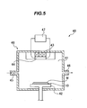
- a PVD (Physical Vapor Deposition) device or a CVD (Chemical Vapor Deposition) device can be employed as film forming means. The case of using a reduced-pressure film-forming device 40 shown in Fig. 5 will be described below.
- a holding portion 42 for holding a flat object in electrostatic fashion is disposed within a sputtering chamber 41, and a sputtering source 44 is disposed at the upper position of this device 40 opposing to the holding portion 42 in a state being supported by an excitation member 43.
- a high-frequency power source 47 is connected across the sputtering source 44.
- an introduction port 45 for introducing a sputtering gas is provided in one side part of the sputtering chamber 41, while a pressure reduction port 46 communicating with a pressure reduction source is provided in the other side part.
- the sputtering chamber 41, excitation member 43, sputtering source 44, introduction port 45, pressure reduction port 46 and high-frequency power source 47 constitute the film forming means 48.
- the back surface of the supporting substrate 10 integrated with the semiconductor wafer W is held on the holding portion 42, whereby the back surface of the semiconductor wafer W is held in opposition to the sputtering source 44.
- the sputtering source 44 magnetized by the excitation member 43 is fed with high-frequency power of about 40 kHz by the high-frequency power source 47, the interior of the sputtering chamber 41 has its pressure reduced on the order of 10 -2 Pa - 10 -4 Pa through the pressure reduction port 46 so as to establish a reduced-pressure environment, and argon gas is introduced through the introduction port 45 so as to generate a plasma.
- argon ions in the plasma collide against the sputtering source 44 and drive out particles, which are deposited on the back surface of the semiconductor wafer W so as to form a film (film formation step).
- the interior of the sputtering chamber 41 is held in the state close to vacuum, and the semiconductor wafer W cannot be held on the holding portion 42 by suction, so that the semiconductor wafer W is electrostatically held.
- a holding force is weaker than in case of a suction type, and hence, the thinned semiconductor wafer W warps.
- the semiconductor wafer W integrated with the supporting substrate 10 can be held through this supporting substrate of high rigidity undergoing no warp. Therefore, even the semiconductor wafer W formed to the thickness of 100 ⁇ m - 15 ⁇ m or so by the thinning work does not warp. Accordingly, the uniform film can be formed on the back surface of the semiconductor wafer W at high precision.
- a film formation step is carried out in a state where the semiconductor wafer is supported by a supporting substrate of high rigidity, so that even the semiconductor wafer processed to be as very thin as 100 ⁇ m or less at a thinning step does not warp. Accordingly, a uniform film can be formed even on the back surface of the very thin semiconductor wafer, and it is permitted to make the structure of the semiconductor wafer thin still further.
- the film formation step is performed in a reduced-pressure environment, there is brought forth the advantage that the film can be formed without warping, although the semiconductor wafer cannot be held by suction.
Landscapes
- Engineering & Computer Science (AREA)
- Mechanical Engineering (AREA)
- Chemical & Material Sciences (AREA)
- Ceramic Engineering (AREA)
- Inorganic Chemistry (AREA)
- Mechanical Treatment Of Semiconductor (AREA)
- Container, Conveyance, Adherence, Positioning, Of Wafer (AREA)
Applications Claiming Priority (3)
| Application Number | Priority Date | Filing Date | Title |
|---|---|---|---|
| JP2002240578 | 2002-08-21 | ||
| JP2002240578A JP2004079889A (ja) | 2002-08-21 | 2002-08-21 | 半導体ウェーハの製造方法 |
| PCT/JP2003/009338 WO2004019388A1 (fr) | 2002-08-21 | 2003-07-23 | Procede de fabrication d'une plaquette a semi-conducteurs |
Publications (2)
| Publication Number | Publication Date |
|---|---|
| EP1548801A1 true EP1548801A1 (fr) | 2005-06-29 |
| EP1548801A4 EP1548801A4 (fr) | 2010-09-01 |
Family
ID=31943938
Family Applications (1)
| Application Number | Title | Priority Date | Filing Date |
|---|---|---|---|
| EP03792633A Withdrawn EP1548801A4 (fr) | 2002-08-21 | 2003-07-23 | Procede de fabrication d'une plaquette a semi-conducteurs |
Country Status (6)
| Country | Link |
|---|---|
| EP (1) | EP1548801A4 (fr) |
| JP (1) | JP2004079889A (fr) |
| KR (1) | KR20050030630A (fr) |
| CN (1) | CN1675745A (fr) |
| AU (1) | AU2003252248A1 (fr) |
| WO (1) | WO2004019388A1 (fr) |
Cited By (3)
| Publication number | Priority date | Publication date | Assignee | Title |
|---|---|---|---|---|
| EP1779969A1 (fr) * | 2005-10-31 | 2007-05-02 | Tokyo Seimitsu Co.,Ltd. | Procédé et dispositif pour meuler la surface arrière d'une plaquette semi-conductrice |
| DE102004038339B4 (de) * | 2003-08-12 | 2011-04-07 | Disco Corp. | Waferbearbeitungsverfahren |
| US9573835B2 (en) | 2011-05-27 | 2017-02-21 | Corning Incorporated | Non-polished glass wafer, thinning system and method for using the non-polished glass wafer to thin a semiconductor wafer |
Families Citing this family (5)
| Publication number | Priority date | Publication date | Assignee | Title |
|---|---|---|---|---|
| JP4416108B2 (ja) * | 2003-11-17 | 2010-02-17 | 株式会社ディスコ | 半導体ウェーハの製造方法 |
| JP5034488B2 (ja) * | 2006-12-25 | 2012-09-26 | 株式会社デンソー | 半導体装置の製造方法 |
| JP5495647B2 (ja) * | 2009-07-17 | 2014-05-21 | 株式会社ディスコ | ウェーハの加工方法 |
| DE102010007127A1 (de) * | 2010-02-05 | 2011-08-11 | Ev Group E. Thallner Gmbh | Verfahren zur Behandlung eines temporär gebondeten Produktwafers |
| JP5965676B2 (ja) * | 2012-03-06 | 2016-08-10 | 株式会社アルバック | 処理対象物の保持方法 |
Family Cites Families (9)
| Publication number | Priority date | Publication date | Assignee | Title |
|---|---|---|---|---|
| US5476566A (en) * | 1992-09-02 | 1995-12-19 | Motorola, Inc. | Method for thinning a semiconductor wafer |
| US5268065A (en) * | 1992-12-21 | 1993-12-07 | Motorola, Inc. | Method for thinning a semiconductor wafer |
| JP2000040677A (ja) * | 1998-07-23 | 2000-02-08 | Nippon Telegr & Teleph Corp <Ntt> | 半導体素子の製造方法 |
| JP3768069B2 (ja) * | 2000-05-16 | 2006-04-19 | 信越半導体株式会社 | 半導体ウエーハの薄型化方法 |
| US6743697B2 (en) * | 2000-06-30 | 2004-06-01 | Intel Corporation | Thin silicon circuits and method for making the same |
| JP2002075940A (ja) * | 2000-08-25 | 2002-03-15 | Hitachi Ltd | 半導体装置の製造方法 |
| JP2002075937A (ja) * | 2000-08-30 | 2002-03-15 | Nitto Denko Corp | 半導体ウエハの加工方法 |
| JP4462755B2 (ja) * | 2000-12-15 | 2010-05-12 | 京セラ株式会社 | ウエハー支持基板 |
| JP2002203821A (ja) * | 2000-12-28 | 2002-07-19 | Mitsubishi Gas Chem Co Inc | 接着および剥離法 |
-
2002
- 2002-08-21 JP JP2002240578A patent/JP2004079889A/ja active Pending
-
2003
- 2003-07-23 KR KR1020057001024A patent/KR20050030630A/ko not_active Ceased
- 2003-07-23 CN CNA03819600XA patent/CN1675745A/zh active Pending
- 2003-07-23 AU AU2003252248A patent/AU2003252248A1/en not_active Abandoned
- 2003-07-23 WO PCT/JP2003/009338 patent/WO2004019388A1/fr not_active Ceased
- 2003-07-23 EP EP03792633A patent/EP1548801A4/fr not_active Withdrawn
Cited By (4)
| Publication number | Priority date | Publication date | Assignee | Title |
|---|---|---|---|---|
| DE102004038339B4 (de) * | 2003-08-12 | 2011-04-07 | Disco Corp. | Waferbearbeitungsverfahren |
| EP1779969A1 (fr) * | 2005-10-31 | 2007-05-02 | Tokyo Seimitsu Co.,Ltd. | Procédé et dispositif pour meuler la surface arrière d'une plaquette semi-conductrice |
| US7601615B2 (en) | 2005-10-31 | 2009-10-13 | Tokyo Seimitsu Co., Ltd. | Method of grinding back surface of semiconductor wafer and semiconductor wafer grinding apparatus |
| US9573835B2 (en) | 2011-05-27 | 2017-02-21 | Corning Incorporated | Non-polished glass wafer, thinning system and method for using the non-polished glass wafer to thin a semiconductor wafer |
Also Published As
| Publication number | Publication date |
|---|---|
| JP2004079889A (ja) | 2004-03-11 |
| WO2004019388A1 (fr) | 2004-03-04 |
| CN1675745A (zh) | 2005-09-28 |
| KR20050030630A (ko) | 2005-03-30 |
| AU2003252248A1 (en) | 2004-03-11 |
| EP1548801A4 (fr) | 2010-09-01 |
Similar Documents
| Publication | Publication Date | Title |
|---|---|---|
| US12300662B2 (en) | DBI to SI bonding for simplified handle wafer | |
| US7183178B2 (en) | Method of manufacturing semiconductor wafer | |
| JP5331500B2 (ja) | ウエーハの処理方法 | |
| JP4647228B2 (ja) | ウェーハの加工方法 | |
| CN102136413B (zh) | 倒角基板布线方法 | |
| CN110214369A (zh) | 用于键合芯片的方法和装置 | |
| US6511895B2 (en) | Semiconductor wafer turning process | |
| JP2009043992A (ja) | ウエーハの加工方法 | |
| WO2003058697A1 (fr) | Procede de fabrication d'une microplaquete semi-conductrice | |
| EP1548801A1 (fr) | Procede de fabrication d'une plaquette a semi-conducteurs | |
| JP2000150836A (ja) | 試料の処理システム | |
| JP4791772B2 (ja) | ウェーハの加工方法 | |
| US20050233548A1 (en) | Method for fabricating semiconductor wafer | |
| TWI241684B (en) | Manufacturing method of semiconductor wafer | |
| TWI788605B (zh) | 晶圓的加工方法 | |
| JP2002016021A (ja) | 半導体チップの生産方法及び半導体チップ | |
| JP2006303329A (ja) | シリコン基板の薄板加工方法およびそれに用いられる加工装置 | |
| JP2004186430A (ja) | 半導体ウェーハの加工方法 | |
| JP2005064234A (ja) | プラズマエッチング方法及びプラズマエッチング装置 | |
| CN117751441A (zh) | 用于制造系统机器人的静电终端受动器 | |
| US6743697B2 (en) | Thin silicon circuits and method for making the same | |
| JP6746230B2 (ja) | ウェーハの製造方法 | |
| US7157376B1 (en) | Method and apparatus for handling thin semiconductor wafers | |
| JP2004221175A (ja) | プラズマエッチング方法及びプラズマエッチング装置 | |
| CN102347213B (zh) | 薄化晶片的方法 |
Legal Events
| Date | Code | Title | Description |
|---|---|---|---|
| PUAI | Public reference made under article 153(3) epc to a published international application that has entered the european phase |
Free format text: ORIGINAL CODE: 0009012 |
|
| 17P | Request for examination filed |
Effective date: 20050315 |
|
| AK | Designated contracting states |
Kind code of ref document: A1 Designated state(s): AT BE BG CH CY CZ DE DK EE ES FI FR GB GR HU IE IT LI LU MC NL PT RO SE SI SK TR |
|
| AX | Request for extension of the european patent |
Extension state: AL LT LV MK |
|
| DAX | Request for extension of the european patent (deleted) | ||
| A4 | Supplementary search report drawn up and despatched |
Effective date: 20100803 |
|
| RIC1 | Information provided on ipc code assigned before grant |
Ipc: H01L 21/68 20060101ALI20100728BHEP Ipc: B24B 7/22 20060101ALI20100728BHEP Ipc: B24B 1/00 20060101ALI20100728BHEP Ipc: H01L 21/304 20060101AFI20100728BHEP |
|
| STAA | Information on the status of an ep patent application or granted ep patent |
Free format text: STATUS: THE APPLICATION IS DEEMED TO BE WITHDRAWN |
|
| 18D | Application deemed to be withdrawn |
Effective date: 20101031 |