EP1538668B1 - Organische elektrolumineszente Vorrichtung - Google Patents
Organische elektrolumineszente Vorrichtung Download PDFInfo
- Publication number
- EP1538668B1 EP1538668B1 EP04028436.6A EP04028436A EP1538668B1 EP 1538668 B1 EP1538668 B1 EP 1538668B1 EP 04028436 A EP04028436 A EP 04028436A EP 1538668 B1 EP1538668 B1 EP 1538668B1
- Authority
- EP
- European Patent Office
- Prior art keywords
- organic
- panel
- display
- cathode
- substrate
- Prior art date
- Legal status (The legal status is an assumption and is not a legal conclusion. Google has not performed a legal analysis and makes no representation as to the accuracy of the status listed.)
- Expired - Lifetime
Links
Images






Classifications
-
- H—ELECTRICITY
- H10—SEMICONDUCTOR DEVICES; ELECTRIC SOLID-STATE DEVICES NOT OTHERWISE PROVIDED FOR
- H10K—ORGANIC ELECTRIC SOLID-STATE DEVICES
- H10K59/00—Integrated devices, or assemblies of multiple devices, comprising at least one organic light-emitting element covered by group H10K50/00
- H10K59/10—OLED displays
- H10K59/12—Active-matrix OLED [AMOLED] displays
- H10K59/128—Active-matrix OLED [AMOLED] displays comprising two independent displays, e.g. for emitting information from two major sides of the display
-
- H—ELECTRICITY
- H05—ELECTRIC TECHNIQUES NOT OTHERWISE PROVIDED FOR
- H05B—ELECTRIC HEATING; ELECTRIC LIGHT SOURCES NOT OTHERWISE PROVIDED FOR; CIRCUIT ARRANGEMENTS FOR ELECTRIC LIGHT SOURCES, IN GENERAL
- H05B33/00—Electroluminescent light sources
-
- H—ELECTRICITY
- H10—SEMICONDUCTOR DEVICES; ELECTRIC SOLID-STATE DEVICES NOT OTHERWISE PROVIDED FOR
- H10K—ORGANIC ELECTRIC SOLID-STATE DEVICES
- H10K59/00—Integrated devices, or assemblies of multiple devices, comprising at least one organic light-emitting element covered by group H10K50/00
- H10K59/10—OLED displays
- H10K59/17—Passive-matrix OLED displays
- H10K59/176—Passive-matrix OLED displays comprising two independent displays, e.g. for emitting information from two major sides of the display
-
- H—ELECTRICITY
- H10—SEMICONDUCTOR DEVICES; ELECTRIC SOLID-STATE DEVICES NOT OTHERWISE PROVIDED FOR
- H10K—ORGANIC ELECTRIC SOLID-STATE DEVICES
- H10K59/00—Integrated devices, or assemblies of multiple devices, comprising at least one organic light-emitting element covered by group H10K50/00
- H10K59/90—Assemblies of multiple devices comprising at least one organic light-emitting element
- H10K59/95—Assemblies of multiple devices comprising at least one organic light-emitting element wherein all light-emitting elements are organic, e.g. assembled OLED displays
-
- H—ELECTRICITY
- H10—SEMICONDUCTOR DEVICES; ELECTRIC SOLID-STATE DEVICES NOT OTHERWISE PROVIDED FOR
- H10K—ORGANIC ELECTRIC SOLID-STATE DEVICES
- H10K2102/00—Constructional details relating to the organic devices covered by this subclass
- H10K2102/301—Details of OLEDs
- H10K2102/302—Details of OLEDs of OLED structures
- H10K2102/3023—Direction of light emission
- H10K2102/3026—Top emission
-
- H—ELECTRICITY
- H10—SEMICONDUCTOR DEVICES; ELECTRIC SOLID-STATE DEVICES NOT OTHERWISE PROVIDED FOR
- H10K—ORGANIC ELECTRIC SOLID-STATE DEVICES
- H10K59/00—Integrated devices, or assemblies of multiple devices, comprising at least one organic light-emitting element covered by group H10K50/00
- H10K59/80—Constructional details
- H10K59/805—Electrodes
- H10K59/8052—Cathodes
- H10K59/80524—Transparent cathodes, e.g. comprising thin metal layers
-
- H—ELECTRICITY
- H10—SEMICONDUCTOR DEVICES; ELECTRIC SOLID-STATE DEVICES NOT OTHERWISE PROVIDED FOR
- H10K—ORGANIC ELECTRIC SOLID-STATE DEVICES
- H10K85/00—Organic materials used in the body or electrodes of devices covered by this subclass
- H10K85/30—Coordination compounds
- H10K85/311—Phthalocyanine
-
- H—ELECTRICITY
- H10—SEMICONDUCTOR DEVICES; ELECTRIC SOLID-STATE DEVICES NOT OTHERWISE PROVIDED FOR
- H10K—ORGANIC ELECTRIC SOLID-STATE DEVICES
- H10K85/00—Organic materials used in the body or electrodes of devices covered by this subclass
- H10K85/30—Coordination compounds
- H10K85/321—Metal complexes comprising a group IIIA element, e.g. Tris (8-hydroxyquinoline) gallium [Gaq3]
- H10K85/324—Metal complexes comprising a group IIIA element, e.g. Tris (8-hydroxyquinoline) gallium [Gaq3] comprising aluminium, e.g. Alq3
-
- H—ELECTRICITY
- H10—SEMICONDUCTOR DEVICES; ELECTRIC SOLID-STATE DEVICES NOT OTHERWISE PROVIDED FOR
- H10K—ORGANIC ELECTRIC SOLID-STATE DEVICES
- H10K85/00—Organic materials used in the body or electrodes of devices covered by this subclass
- H10K85/60—Organic compounds having low molecular weight
- H10K85/615—Polycyclic condensed aromatic hydrocarbons, e.g. anthracene
-
- H—ELECTRICITY
- H10—SEMICONDUCTOR DEVICES; ELECTRIC SOLID-STATE DEVICES NOT OTHERWISE PROVIDED FOR
- H10K—ORGANIC ELECTRIC SOLID-STATE DEVICES
- H10K85/00—Organic materials used in the body or electrodes of devices covered by this subclass
- H10K85/60—Organic compounds having low molecular weight
- H10K85/631—Amine compounds having at least two aryl rest on at least one amine-nitrogen atom, e.g. triphenylamine
Definitions
- the present invention relates to an organic EL device, and more particularly, to an organic EL device and a driving apparatus thereof.
- an organic electroluminescent (EL) device is a device to emit light while a pair of electron and hole formed by injecting a charge into a light emitting layer of an organic material disposed between the electron injection electrode (cathode) and the hole injection electrode (anode).
- Such an organic EL device is characterized by operation at a relatively low voltage and low power consumption.
- the organic EL devices for a unidirectional display can be classified into a bottom emission type and a top emission type.
- FIG. 1 A bottom emission type organic EL device is shown in FIG. 1 .
- a method of fabricating the bottom emission type organic EL device shown in FIG. 1 will now be described.
- An anode 2 is formed on a transparent substrate 1.
- the anode 2 is generally made of indium tin oxide (ITO).
- HIL hole injecting layer
- the HIL 3 is generally made of copper phthalocyanine (CuPc) and is coated to a thickness of 10 - 30 nm.
- CuPc copper phthalocyanine
- HTL hole transport layer
- the HTL is generally made of TPD (N'-diphenyl-N,N'-bis(3-methylphenyl)-(1-1'-biphenyl)4,4'-diamine) or NPD (4,4'-bis[N-(1-naphthyl)-N-phenyl-amino]biphenyl), and is deposited to a thickness of 30 - 60 nm.
- TPD N'-diphenyl-N,N'-bis(3-methylphenyl)-(1-1'-biphenyl)4,4'-diamine
- NPD 4,4'-diamine
- NPD 4,4'-bis[N-(1-naphthyl)-N-phenyl-amino]biphenyl
- an organic emitting layer 5 made of an organic material is formed on the HTL4.
- the organic emitting layer 5 as formed may contain dopants if necessary.
- Alq 3 ⁇ tris(8-hydroxy-quinolate)aluminum ⁇ is deposited to about 30 - 60 nm so as to form the organic emitting layer 5, and coumarin 6 or Qd (Quinacridone) is added as the dopants.
- ECM In case of red light emission, ECM, DCJT, DCJTB or the like is used.
- the structure of Alq 3 is also shown in FIG. 8 .
- an electron transport layer (ETL) 6 and an electron injecting layer (EIL) 7 are continuously formed on the organic emitting layer 5, or the ETL 6 and the EIL 7 are formed together with an electron injection transport layer.
- the EIL 7 is formed by coating LiF or Li 2 O to a thickness of about 5 ⁇ , or by depositing alkali metal or alkaline-earth metal such as Li, CA, Mg, Sm, etc. to a thickness less than 200A for making electron injection better.
- the EIL 7 and the ETL 6 may be not used.
- the material layer used as the cathode serves as a mirror reflection surface.
- the remaining half of the light is reflected by the cathode and emits toward the transparent electrode (anode).
- FIG. 2 a top emission type organic EL device is shown in FIG. 2 .
- a method of fabricating the top emission type organic EL device shown in FIG. 2 will now be described.
- an organic EL device is formed on an opaque substrate and a transparent electrode is lastly formed such that light emits in an opposite direction to the substrate.
- An anode 12 is first formed on an opaque substrate 11.
- hole injecting layers (HILs) 13 and 14 are formed on the anode 12.
- an organic emitting layer 15 made of an organic material is formed on the HTL 14.
- an electron transport layer (ETL) 16 and an electron injecting layer (EIL) 17 are formed on the organic emitting layer 15.
- a transparent cathode 18 is formed on the EIL 17 such that light is irradiated upward.
- FIG. 3 is a sectional view of a bidirectional organic EL according to the related art.
- the organic EL device for bidirectional display employs the bottom emission type shown in FIG. 1 at the lower side from an emitting layer 25 and the top emission type shown in FIG. 2 at the upper side from the emitting layer 25 such that light emits in both directions of upper and lower sides.
- the organic EL device for bidirectional display needs a power at least four times greater than that of the bottom emission type organic EL device so as to obtain the same brightness.
- the organic EL device for bidirectional display is driven by a pair of electrodes, it is possible to display an identical picture in the upper and lower directions, but it is impossible to display different pictures on the upper screen and the lower screen.
- EP 1 071 313 A1 describes an electroluminescence element and a lighting unit having the same.
- an electroluminescence element has a laminated structure of a flexible light-transmittable insulating film made of polyethylene terephtalate or the like; and a light-transmittable insulating front electrode layer, which is made of indium tin oxide, formed on the entirely underneath film by a spattering process or an electron beam process; a luminescent layer dispersed luminous powder, which is luminescent base material such as zinc sulfide, in high dielectric resin such fluoro-contained rubber, cyan-base resin or the like, underneath a front electrode layer, a rear electrode layer dispersed silver or carbon resin, in epoxy resin, polyester or the like; an insulating layer made of epoxy resin, polyester resin or the like.
- two EL elements When illuminating both sides of the electronic device, two EL elements are placed so as to be opposed each insulating layer of two EL elements back to back. When converting color of light and illuminating with multiple-color lights, two EL elements having different luminescent colors are combined.
- JP 2001-345 184 A describes an electroluminescence element and a display device.
- a display device is provided with a light transmissive insulating base, a pair of electrode formed at a prescribed interval on one surface of the insulating base, a dielectric layer formed on at least one electrode of the pair of electrode, a light emitter layer formed on the dielectric layer and a light transmissive sealing layer formed on the light emitting layer.
- two display devices are assembled by bonding the respective insulating bases by means of adhesive.
- WO 03/092332 A describes an organic EL light-emitting device having light-emission characteristics that hardly change with time.
- the device comprises a humid-impermeable insulating transparent substrate, a light-emitting portion of a multilayer structure having a first transparent electrode layer formed on the substrate, an organic EL light-emitting layer formed on the first transparent electrode layer, and a second electrode layer formed on the organic EL light-emitting layer, a humid-impermeable sealing wall defining a space covering the light-emitting portion without extending over the electrodes and provided over the substrate, and connection terminals connected to the outside through the sealing wall or the substrate and adapted to supply electric power to the electrode layers.
- JP 2002-313 571 A describes a multi-color light-emitting display.
- a multi-color light-emitting display is formed by a stack of organic electroluminescent elements having respective transparent substrates, respective transparent anodes, respective transparent cathodes, and respective light-emitting layers.
- the electroluminescent elements whose light-emitting layers emit light of different colors are stacked on one another in the display. Between the respective displays, there is a glue line provided for bonding the respective organic EL devices.
- the multi color luminescence display can be obtained by sticking these by pressure using a rubber roll.
- the present invention is directed to an organic EL device that substantially obviate one or more problems due to limitations and disadvantages of the related art.
- An object of the present invention is to provide an organic EL device having a lower power consumption and high performance and enabling to display separate pictures on bidirectional screens as well as to display the same picture on the bidirectional screens.
- an organic EL device comprising: a first organic EL panel for a unidirectional display; and a second organic EL panel for a unidirectional display, each of the first and second organic EL panels having a substrate, a first electrode, an emitting layer and a second electrode, wherein the first organic EL panel and the second organic EL panel are coupled so as to display pictures in bidirections.
- the first organic EL panel and the second organic EL panel are coupled using a UV hardening material.
- the above organic EL device further comprises a buffer layer for electrical contact of the first organic EL panel and the second organic EL panel.
- the above organic EL device may further comprise an insulating layer for electrical isolation between the first organic EL panel and the second organic EL panel.
- first organic EL panel and the second organic EL panel can be selectively driven to display the same picture or different pictures.
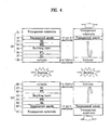
- an organic EL device for bidirectional display is made by bonding a first organic EL panel 30 and a second organic EL panel 30' .
- the first organic EL panel 30 performs a unidirectional display through a transparent anode 32 and a transparent substrate 31, and the second organic EL panel 30' also performs a unidirectional display through a transparent anode 32' and a transparent substrate 31'.
- the first organic EL panel 30 and the second organic EL panel 30' are coupled by bonding a cathode 38 of the first organic EL panel 30 with a cathode 38' of the second organic EL panel 30' for bidirectional display.
- first organic EL panel 30 and the second organic EL panel 30' have the same structure of which upper and lower sides are inverted, their description is made centering on the first organic EL panel 30.
- a transparent anode 32 is formed on a transparent substrate 31.
- the transparent anode 32 is generally made of indium tin oxide (ITO).
- a hole injecting layer (HIL) 33 is formed on the transparent anode 32.
- the HIL 33 is generally made of copper phthalocyanine (CuPc) and is coated to a thickness of 10 - 30 nm.
- CuPc copper phthalocyanine
- HTL 34 is formed on the HIL 33.
- the HTL 33 is generally made of TPD (N'-diphenyl-N,N'-bis(3-methylphenyl)-(1-1'-biphenyl)4,4'-diamine) or NPD (4,4'-bis[N-(1-naphthyl)-N-phenyl-amino]biphenyl), and is deposited to a thickness of 30 - 60 nm.
- TPD N'-diphenyl-N,N'-bis(3-methylphenyl)-(1-1'-biphenyl)4,4'-diamine
- NPD 4,4'-diamine
- the structures of TPD and NPD are shown in FIG. 8 for your understanding.
- an organic emitting layer 35 made of an organic material is formed on the HTL 34.
- the organic emitting layer 35 as formed may contain dopants if necessary.
- Alq 3 ⁇ tris(8-hydroxy-quinolate)aluminum ⁇ is deposited to about 30 - 60 nm so as to form the organic emitting layer 5, and coumarin 6 or Qd (Quinacridone) is added as the dopants.
- ECM In case of red light emission, ECM, DCJT, DCJTB or the like is used.
- the structure of Alq 3 is also shown in FIG. 8 .
- an electron transport layer (ETL) 36 and an electron injecting layer (EIL) 37 are continuously formed on the organic emitting layer 35, or the ETL 36 and the EIL 37 are formed together with an electron injection transport layer.
- the EIL 37 is formed by coating LiF or Li 2 O to a thickness of about 5 ⁇ , or by depositing alkali metal or alkaline-earth metal such as Li, CA, Mg, Sm, etc. to a thickness less than 200 ⁇ for making electron injection better.
- the EIL 7 and the ETL 6 may be not used.
- aluminum (Al) is coated on the EIL 7 to a thickness of about 1000 ⁇ to form a cathode 38, thereby completing the first organic EL panel 30.
- the second organic EL panel 30' is fabricated by the same method as the aforementioned method.
- the cathode 38 of the first organic EL panel 30 is bonded with the cathode 38' of the second organic EL panel 30', thereby completing the fabrication of the organic EL device for bidirectional display.
- the bonding of the first and second organic EL panels 30 and 30' is performed using an ultra violet (UV) hardening material, for example, epoxy-based adhesive.
- UV ultra violet
- a buffer layer for electrical connection of the two EL panels may be further formed between the first organic EL panel 30 and the second organic EL panel 30'.
- an insulating layer for electrical insulation between the two EL panels may be further formed between the first organic EL panel 30 and the second organic EL panel 30'.
- any one of the cathodes of the first and second organic EL panels 30 and 30' may be commonly used.
- any one of the first and second organic EL panels 30 and 30' may not have the cathode.
- the respective emitting layers are provided to display pictures through the transparent anode and the transparent substrate, a sufficient brightness for bidirectional display is obtained, so that a low power operation becomes possible.
- the transparent cathode formed by a sputtering causes a thermal stress to lower the device performance and a transparent passivation layer is further required on the transparent cathode, thereby causing drop of the overall transmittance.
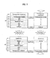
- an organic EL device for bidirectional display is made by bonding a first organic EL panel 40 and a second organic EL panel 40'.
- the first and second organic EL panels 40 and 40' perform a unidirectional display through their respective transparent cathodes 48 and 48'.
- the first organic EL panel 40 and the second organic EL panel 40' are coupled by bonding the transparent cathode 48 of the first organic EL panel 40 and the transparent cathode 48' of the second organic EL panel 40' for bidirectional display.
- first organic EL panel 40 and the second organic EL panel 40' have the same structure of which upper and lower sides are inverted, their description is made centering on the first organic EL panel 40.
- an anode 42 is formed on an opaque substrate 41.
- HIL hole injecting layer
- HTL hole transport layer
- an organic emitting layer 45 made of an organic material is formed on the HTL 44.
- an electron transport layer (ETL) 46 and an electron injecting layer (EIL) 47 are formed on the organic emitting layer 45.
- a transparent cathode 48 is formed on the EIL 47 such that light emits, thereby completing the first organic EL panel 40.
- the second organic EL panel 40' is fabricated by the same method as the aforementioned method.
- the substrate 41 of the first organic EL panel 40 is bonded with the substrate 41' of the second organic EL panel 40', thereby completing the fabrication of the organic EL device for bidirectional display.
- the bonding of the first and second organic EL panels 40 and 40' is performed using an ultra violet (UV) hardening material, for example, epoxy-based adhesive.
- UV ultra violet
- a buffer layer for electrical connection of the two EL panels may be further formed between the first organic EL panel 40 and the second organic EL panel 40'.
- an insulating layer for electrical insulation between the two EL panels may be further formed between the first organic EL panel 40 and the second organic EL panel 40'.
- any one of the substrates of the first and second organic EL panels 40 and 40' may be commonly used.
- the second organic EL panels 40' except for the substrate 41' is formed on an exposed surface of the substrate 41 of the first organic EL panel 40.
- an organic EL device for bidirectional display according to a second embodiment of the present invention is made by bonding a first organic EL panel 40 and a second organic EL panel 30'.
- the first organic EL panel 40 performs a unidirectional display through a transparent cathode 48 and has the same structure as the first organic EL panel 40 of FIG. 5 .
- the second organic EL panel 30' performs a unidirectional display through a transparent anode 32' and a transparent substrate 31' and has the same structure as the second organic EL panel 30' of FIG. 4 .
- first organic EL panel 40 and the second organic EL panel 30' are coupled by bonding the substrate 41 of the first organic EL panel 40 and the cathode 38' of the second organic EL panel 30' for bidirectional display.
- the bonding of the first and second organic EL panels 40 and 30' is performed using an ultra violet (UV) hardening material, for example, epoxy-based adhesive.
- UV ultra violet
- a buffer layer for electrical connection of the two EL panels may be further formed between the first organic EL panel 40 and the second organic EL panel 30'.
- an insulating layer for electrical insulation between the two EL panels may be further formed between the first organic EL panel 40 and the second organic EL panel 30'.
- the respective emitting layers are provided to display pictures through the transparent cathode and the transparent substrate, a sufficient brightness for bidirectional display is obtained, so that a low power operation becomes possible.
- an organic EL device for bidirectional display is made by bonding a first organic EL panel 30 and a second organic EL panel 40'.
- the first organic EL panel 30 performs a unidirectional display through a transparent anode 32 and a transparent substrate 31, and has the same structure as the first organic EL panel 30 of FIG. 4 .
- the second organic EL panel 40' performs a unidirectional display through a transparent cathode 48' and has the same structure as the second organic EL panel 40' of FIG. 5 .
- first organic EL panel 30 and the second organic EL panel 40' are coupled by bonding the cathode 38 of the first organic EL panel 30 and the substrate 40' of the second organic EL panel 40' for bidirectional display.
- the bonding of the first and second organic EL panels 30 and 40' is performed using an ultra violet (UV) hardening material, for example, epoxy-based adhesive.
- UV ultra violet
- a buffer layer for electrical connection of the two EL panels may be further formed between the first organic EL panel 30 and the second organic EL panel 40'.
- an insulating layer for electrical insulation between the two EL panels may be further formed between the first organic EL panel 30 and the second organic EL panel 40'.
- the respective emitting layers are provided to display pictures through the transparent cathode and the transparent substrate, a sufficient brightness for bidirectional display is obtained, so that a low power operation becomes possible.
- a driving apparatus of an organic EL device includes an organic EL device, a driving unit 50, a switching unit 60 and a controller 70.
- the driving apparatus may be used in all organic EL devices each having first and second electrodes and operatable separately as well as in the organic EL devices fabricated according to the first to third embodiments of the present invention.
- the driving unit 50 outputs first and second driving signals such that the organic EL device can display pictures.
- the driving unit 50 may be constructed to output only one driving signal or two or more driving signals.
- the switching unit 60 supplies at least one of the first and second organic EL panels with the first and second driving signals outputted from the driving unit 50 according to a control signal.
- the switching unit 60 includes first and second input terminals receiving the first and second driving signals outputted from the driving unit 50, a first output terminal outputting one of the first and second driving signals to the first organic EL panel, a second output terminal outputting one of the first and second driving signals to the second organic EL panel, a third output terminal concurrently outputting one of the first and second driving signals to the first organic EL panel and the second organic EL panel, a switch 61 selectively connecting the first and second input terminals with the first to third output terminals, and a diode connected to the third output terminal, for preventing a signal transmission error between the first output terminal and the second output terminal.
- the switching unit 60 may be designed having a different construction depending on the number of the signals outputted from the driving unit 50.
- the controller 70 controls the switching unit 60 according to a preset program or an external control.
- the preset program is to automatically perform a picture display. For example, there are the same picture display setting in bidirections, a different picture display setting in bidirections, or a unidirectional picture display setting.
- the external control means a control signal of when a user manually selects one of the picture display settings.
- the organic EL device can display different pictures with respect to the first and second organic EL panels as well as perform bidirectional display.
- the controller 70 controls the switch 61 shown in FIG. 10 such that the first driving signal (or second driving signal) is supplied to the first organic EL panel and the second organic EL panel at the same time.
- the first and second organic EL panels operate according to the first driving signal to display the same picture.
- the controller 70 controls the switch 61 shown in FIG. 10 such that the first driving signal (or second driving signal) is supplied to the first organic EL panel through the first output terminal.
- the controller 70 controls the switch 61 such that the second driving signal (or first driving signal) is supplied to the second organic EL panel through the second output terminal.
- the first and second organic EL panels operate according to the first driving signal and the second driving signal to display the respective different pictures thereon.
- the controller 70 controls the switch 61 shown in FIG. 10 such that the first driving signal is supplied to the first organic EL panel through the first output terminal.
- the first organic EL panel operates according to the first driving signal to display a picture thereon.
- the second organic EL panel does not display a picture.
- a selected picture is displayed on a selected panel but a picture is not displayed on a non-selected panel.
Landscapes
- Engineering & Computer Science (AREA)
- Microelectronics & Electronic Packaging (AREA)
- Electroluminescent Light Sources (AREA)
- Devices For Indicating Variable Information By Combining Individual Elements (AREA)
- Control Of Indicators Other Than Cathode Ray Tubes (AREA)
- Control Of El Displays (AREA)
Claims (3)
- Organische EL-Vorrichtung, die umfasst:- eine erste organische EL-Tafel (30), die ein erstes Substrat (31), eine erste Anode (32), eine erste Emissionsschicht (35) und eine erste Katode (38) aufweist;- eine zweite organische EL-Tafel (30'), die ein zweites Substrat (31'), eine zweite Anode (32'), eine zweite Emissionsschicht (35') und eine zweite Katode (38') aufweist;- ein UV-aushärtendes Material, um die erste Katode (38) und die zweite Katode (38') zu verbinden,- wobei die erste organische EL-Tafel (30) und die zweite organische EL-Tafel (30') gekoppelt sind, um Bilder in zwei Richtungen anzuzeigen, gekennzeichnet durch- eine Pufferschicht, die zwischen der ersten Katode (38) und der zweiten Katode (38') ausgebildet ist, wobei die erste Katode (38) durch die Pufferschicht mit der zweiten Katode (38') elektrisch verbunden ist.
- Organische EL-Vorrichtung, die umfasst:- eine erste organische EL-Tafel (40), die ein erstes Substrat (41), eine erste Anode (42), eine erste Emissionsschicht (45) und eine erste Katode (48) aufweist;- eine zweite organische EL-Tafel (30'), die ein zweites Substrat (31'), eine zweite Anode (32'), eine zweite Emissionsschicht (35') und eine zweite Katode (38') aufweist;- ein UV-aushärtendes Material, um das erste Substrat (41) der ersten organischen EL-Tafel (40) und die zweite Katode (38') der zweiten organischen EL-Tafel (30') zu verbinden;- wobei die erste organische EL-Tafel (30) und die zweite organische EL-Tafel (30') gekoppelt sind, um Bilder in zwei Richtungen anzuzeigen; gekennzeichnet durch- eine Pufferschicht, die zwischen dem ersten Substrat (41) der ersten organischen EL-Tafel (40) und der zweiten Katode (38') der zweiten organischen EL-Tafel (30') ausgebildet ist, wobei das erste Substrat (41) der ersten organischen EL-Tafel (40) durch die Pufferschicht mit der zweiten Katode (38') der zweiten organischen EL-Tafel (30') elektrisch verbunden und verbunden ist.
- Organische EL-Vorrichtung, die umfasst:- eine erste organische EL-Tafel (30), die ein erstes Substrat (31), eine erste Anode (32), eine erste Emissionsschicht (35) und eine erste Katode (38) aufweist;- eine zweite organische EL-Tafel (40'), die ein zweites Substrat (41'), eine zweite Anode (42'), eine zweite Emissionsschicht (45') und eine zweite Katode (48') aufweist;- ein UV-aushärtendes Material, um die erste Katode (38) der ersten organischen EL-Tafel (30) und das zweite Substrat (41') der zweiten organischen EL-Tafel (40') zu verbinden;- wobei die erste organische EL-Tafel (30) und die zweite organische EL-Tafel (30') gekoppelt sind, um Bilder in zwei Richtungen anzuzeigen; gekennzeichnet durch- eine Pufferschicht, die zwischen der ersten Katode (38) der ersten organischen EL-Tafel (30) und dem zweiten Substrat (41') der zweiten organischen EL-Tafel (40') ausgebildet ist, wobei die erste Katode (38) der ersten organischen EL-Tafel (30) durch die Pufferschicht mit dem zweiten Substrat (41') der zweiten organischen EL-Tafel (40') elektrisch verbunden ist.
Applications Claiming Priority (2)
| Application Number | Priority Date | Filing Date | Title |
|---|---|---|---|
| KR2003086839 | 2003-12-02 | ||
| KR1020030086839A KR100565639B1 (ko) | 2003-12-02 | 2003-12-02 | 유기 el 소자 |
Publications (3)
| Publication Number | Publication Date |
|---|---|
| EP1538668A2 EP1538668A2 (de) | 2005-06-08 |
| EP1538668A3 EP1538668A3 (de) | 2006-12-27 |
| EP1538668B1 true EP1538668B1 (de) | 2015-06-24 |
Family
ID=34464797
Family Applications (1)
| Application Number | Title | Priority Date | Filing Date |
|---|---|---|---|
| EP04028436.6A Expired - Lifetime EP1538668B1 (de) | 2003-12-02 | 2004-12-01 | Organische elektrolumineszente Vorrichtung |
Country Status (5)
| Country | Link |
|---|---|
| US (1) | US7557512B2 (de) |
| EP (1) | EP1538668B1 (de) |
| JP (1) | JP2005166672A (de) |
| KR (1) | KR100565639B1 (de) |
| CN (1) | CN100576597C (de) |
Families Citing this family (13)
| Publication number | Priority date | Publication date | Assignee | Title |
|---|---|---|---|---|
| US8263968B2 (en) * | 2005-10-31 | 2012-09-11 | The Hong Kong University Of Science And Technology | Double sided emission organic light emitting diode display |
| DE102005057699B4 (de) * | 2005-11-29 | 2012-08-16 | Fraunhofer-Gesellschaft zur Förderung der angewandten Forschung e.V. | Selbstleuchtende Vorrichtung |
| US8008851B2 (en) | 2006-01-19 | 2011-08-30 | Lg Display Co., Ltd. | Organic light emitting display |
| KR100770127B1 (ko) * | 2006-11-10 | 2007-10-24 | 삼성에스디아이 주식회사 | 유기 전계 발광 표시 장치 및 그 제조 방법 |
| US7498603B2 (en) * | 2006-12-06 | 2009-03-03 | General Electric Company | Color tunable illumination source and method for controlled illumination |
| EP2257984A1 (de) * | 2008-02-22 | 2010-12-08 | Philips Intellectual Property & Standards GmbH | Zweiseitige organische lichtemittierende diode (oled) |
| WO2012047208A1 (en) * | 2010-10-05 | 2012-04-12 | Hewlett-Packard Development Company, L.P. | Bidirectional display for a portable electronic device |
| US20130154471A1 (en) * | 2011-12-15 | 2013-06-20 | General Electric Company | Oled devices |
| JP2012118552A (ja) * | 2012-01-16 | 2012-06-21 | Global Oled Technology Llc | デュアルディスプレイ装置 |
| TWI478623B (zh) | 2012-02-13 | 2015-03-21 | 元太科技工業股份有限公司 | 顯示器 |
| KR102046157B1 (ko) * | 2012-12-21 | 2019-12-03 | 삼성디스플레이 주식회사 | 유기 발광 표시 장치 및 그 제조 방법 |
| JP6106474B2 (ja) * | 2013-03-13 | 2017-03-29 | 株式会社カネカ | 有機el装置 |
| KR102287012B1 (ko) * | 2014-05-28 | 2021-08-09 | 덕산네오룩스 주식회사 | 유기전기 소자용 화합물, 이를 이용한 유기전기소자 및 그 전자 장치 |
Citations (2)
| Publication number | Priority date | Publication date | Assignee | Title |
|---|---|---|---|---|
| JP2001345184A (ja) * | 2000-06-01 | 2001-12-14 | Nippon Menbrane:Kk | エレクトロルミネセンス素子及び表示装置 |
| JP2002313571A (ja) * | 2001-04-17 | 2002-10-25 | Tokai Rubber Ind Ltd | 多色発光ディスプレイ |
Family Cites Families (34)
| Publication number | Priority date | Publication date | Assignee | Title |
|---|---|---|---|---|
| JPH074793Y2 (ja) | 1989-04-13 | 1995-02-01 | 株式会社小糸製作所 | El素子の構造 |
| US5359261A (en) | 1990-12-28 | 1994-10-25 | Stanley Electric Co., Ltd. | Electroluminescence display |
| JPH06223966A (ja) | 1993-01-28 | 1994-08-12 | Toshiba Corp | 有機分散型elパネル |
| FR2726126A1 (fr) * | 1994-10-24 | 1996-04-26 | Mitsubishi Electric Corp | Procede de fabrication de dispositifs a diodes electroluminescentes a lumiere visible |
| US5965907A (en) * | 1997-09-29 | 1999-10-12 | Motorola, Inc. | Full color organic light emitting backlight device for liquid crystal display applications |
| JPH11190979A (ja) | 1997-12-26 | 1999-07-13 | Hitachi Electron Service Co Ltd | 複数の表示装置を備えた情報処理装置 |
| JP2000058260A (ja) | 1998-08-07 | 2000-02-25 | Mitsubishi Electric Corp | 両面発光型エレクトロルミネッセンス素子および両面自発光型情報表示素子 |
| JP2000100558A (ja) | 1998-09-18 | 2000-04-07 | Matsushita Electric Ind Co Ltd | 発光装置 |
| JP2000100560A (ja) | 1998-09-21 | 2000-04-07 | Matsushita Electric Ind Co Ltd | 発光装置 |
| JP2001035652A (ja) | 1999-07-21 | 2001-02-09 | Matsushita Electric Ind Co Ltd | エレクトロルミネッセンス素子及びこれを用いた照光ユニット |
| KR100444694B1 (ko) | 1999-08-04 | 2004-08-18 | 엘지전자 주식회사 | 폴더형 이동 통신 단말기의 표시장치 |
| JP3758930B2 (ja) * | 2000-03-17 | 2006-03-22 | 三星エスディアイ株式会社 | 画像表示装置及びその駆動方法 |
| JP2001306000A (ja) * | 2000-04-21 | 2001-11-02 | Minolta Co Ltd | 積層型表示パネル及びその製造方法 |
| JP3875470B2 (ja) * | 2000-08-29 | 2007-01-31 | 三星エスディアイ株式会社 | ディスプレイの駆動回路及び表示装置 |
| US6771327B2 (en) * | 2000-09-18 | 2004-08-03 | Citizen Watch Co., Ltd. | Liquid crystal display device with an input panel |
| JP2002123208A (ja) * | 2000-10-13 | 2002-04-26 | Nec Corp | 画像表示装置およびその駆動方法 |
| KR100720411B1 (ko) * | 2000-10-25 | 2007-05-22 | 엘지.필립스 엘시디 주식회사 | 액정 디스플레이 패널 및 그 제조방법 |
| JP2003066859A (ja) | 2001-08-28 | 2003-03-05 | Sharp Corp | 表示装置およびその製造方法 |
| US6936856B2 (en) * | 2002-01-15 | 2005-08-30 | Osram Opto Semiconductors Gmbh | Multi substrate organic light emitting devices |
| JP2003229252A (ja) | 2002-02-01 | 2003-08-15 | Sharp Corp | 転写フィルムを用いた有機led素子の製造方法 |
| KR20030068654A (ko) | 2002-02-15 | 2003-08-25 | 주식회사 엘리아테크 | 양면 발광의 유기 전계 발광 표시 소자 제조 방법 |
| JP2003317940A (ja) | 2002-04-25 | 2003-11-07 | Harison Toshiba Lighting Corp | 有機エレクトロルミネッセンス発光装置 |
| US20060087224A1 (en) | 2002-04-25 | 2006-04-27 | Harison Toshiba Lighting Corporation | Organic electroluminescence light-emitting device |
| JP2003338366A (ja) | 2002-05-21 | 2003-11-28 | Seiko Instruments Inc | El装置、el装置の製造方法、及びel表示装置 |
| JP2004014316A (ja) * | 2002-06-07 | 2004-01-15 | Rohm Co Ltd | 両面表示有機エレクトロルミネセンスディスプレイモジュール及び情報端末 |
| KR20040009348A (ko) * | 2002-07-23 | 2004-01-31 | 삼성 엔이씨 모바일 디스플레이 주식회사 | 듀얼 타입 유기전자발광소자와 그 제조방법 |
| KR100846581B1 (ko) * | 2002-09-19 | 2008-07-16 | 삼성에스디아이 주식회사 | 듀얼형 유기전자발광소자와 그 제조방법 |
| US7158161B2 (en) * | 2002-09-20 | 2007-01-02 | Matsushita Electric Industrial Co., Ltd. | Organic electroluminescence element and an exposure unit and image-forming apparatus both using the element |
| US6771020B1 (en) * | 2003-02-21 | 2004-08-03 | Wintek Corporation | Double-face lighting electro luminescent device |
| TW586096B (en) * | 2003-04-25 | 2004-05-01 | Ind Tech Res Inst | Dual-screen organic electroluminescent display |
| US20050007517A1 (en) * | 2003-07-08 | 2005-01-13 | Organic Lighting Technologies Llc | Organic light emitting diode backlight integrated LCD |
| JP2005084642A (ja) | 2003-09-11 | 2005-03-31 | Tohoku Pioneer Corp | 両面表示装置及びその製造方法 |
| KR100552968B1 (ko) | 2003-09-23 | 2006-02-15 | 삼성에스디아이 주식회사 | 액티브 매트릭스 유기전계 발광표시장치 |
| KR100934155B1 (ko) | 2003-10-10 | 2009-12-29 | 에스케이씨 주식회사 | 양면발광 유기전계 발광표시 장치 |
-
2003
- 2003-12-02 KR KR1020030086839A patent/KR100565639B1/ko not_active Expired - Lifetime
-
2004
- 2004-12-01 US US11/000,009 patent/US7557512B2/en not_active Expired - Lifetime
- 2004-12-01 EP EP04028436.6A patent/EP1538668B1/de not_active Expired - Lifetime
- 2004-12-02 CN CN200410095619A patent/CN100576597C/zh not_active Expired - Lifetime
- 2004-12-02 JP JP2004349954A patent/JP2005166672A/ja active Pending
Patent Citations (2)
| Publication number | Priority date | Publication date | Assignee | Title |
|---|---|---|---|---|
| JP2001345184A (ja) * | 2000-06-01 | 2001-12-14 | Nippon Menbrane:Kk | エレクトロルミネセンス素子及び表示装置 |
| JP2002313571A (ja) * | 2001-04-17 | 2002-10-25 | Tokai Rubber Ind Ltd | 多色発光ディスプレイ |
Also Published As
| Publication number | Publication date |
|---|---|
| EP1538668A3 (de) | 2006-12-27 |
| EP1538668A2 (de) | 2005-06-08 |
| US7557512B2 (en) | 2009-07-07 |
| KR20050053210A (ko) | 2005-06-08 |
| US20050116659A1 (en) | 2005-06-02 |
| JP2005166672A (ja) | 2005-06-23 |
| CN100576597C (zh) | 2009-12-30 |
| CN1625316A (zh) | 2005-06-08 |
| KR100565639B1 (ko) | 2006-03-29 |
Similar Documents
| Publication | Publication Date | Title |
|---|---|---|
| US7187118B2 (en) | Dual panel type organic electro luminescent display device and manufacturing method for the same | |
| KR100476572B1 (ko) | 유기 이엘장치 및 그 제조방법 | |
| KR100670543B1 (ko) | 유기전계발광 소자 | |
| TWI448194B (zh) | 有機發光元件,含彼之顯示元件,及含彼之照明裝置 | |
| US20080100209A1 (en) | Organic Electroluminescent Display Device | |
| JP6751459B2 (ja) | 有機エレクトロルミネッセンス照明パネル、その製造方法及び有機エレクトロルミネッセンス照明装置 | |
| JP2000195664A (ja) | 発光装置 | |
| CN109616581B (zh) | 显示面板和显示装置 | |
| US20080074356A1 (en) | Control circuit for stacked oled device | |
| US7557512B2 (en) | Organic electroluminescent device and driving apparatus | |
| JP2009252458A (ja) | 有機エレクトロルミネセンス素子 | |
| JP3669333B2 (ja) | 有機電界発光素子及び表示装置 | |
| EP0905672A1 (de) | Mehrschichtige Anzeigetafelkonstruktion und Steuerverfahren dafür | |
| WO2007097545A1 (en) | Flat light emitting oleds device from combined multiple dual emission transparent oleds | |
| KR20040044066A (ko) | 유기 전계 발광 소자 및 발광 장치 | |
| JPH11312585A (ja) | 有機el素子 | |
| JPH11312584A (ja) | 有機el素子 | |
| JPH08213172A (ja) | 有機エレクトロルミネッセンス素子 | |
| US20040196420A1 (en) | Display apparatus with mirror function | |
| JPWO2017203787A1 (ja) | 有機エレクトロルミネッセンス素子 | |
| US20060071885A1 (en) | Self-emission device | |
| WO2017203788A1 (ja) | 有機エレクトロルミネッセンス素子 | |
| JP2002151271A (ja) | 有機el素子及びその製造方法 | |
| KR100571004B1 (ko) | 적층형 유기 전계 발광 소자 | |
| KR20080042008A (ko) | 유기 el 소자 및 유기 el 디스플레이 |
Legal Events
| Date | Code | Title | Description |
|---|---|---|---|
| PUAI | Public reference made under article 153(3) epc to a published international application that has entered the european phase |
Free format text: ORIGINAL CODE: 0009012 |
|
| 17P | Request for examination filed |
Effective date: 20041201 |
|
| AK | Designated contracting states |
Kind code of ref document: A2 Designated state(s): AT BE BG CH CY CZ DE DK EE ES FI FR GB GR HU IE IS IT LI LT LU MC NL PL PT RO SE SI SK TR |
|
| AX | Request for extension of the european patent |
Extension state: AL BA HR LV MK YU |
|
| RIN1 | Information on inventor provided before grant (corrected) |
Inventor name: KIM, HONG GYU Inventor name: KIM, SUNG KAB Inventor name: KYUNG, JAE WOO Inventor name: YANG, JOONG HWAN Inventor name: HAN, YOUNG SOO Inventor name: YOON, JONG GEUN Inventor name: LEE, JAE MAN Inventor name: KIM, MYUNG SEOP |
|
| RIN1 | Information on inventor provided before grant (corrected) |
Inventor name: YOON, JONG GEUN Inventor name: KIM, MYUNG SEOP Inventor name: KYUNG, JAE WOO Inventor name: LEE, JAE MAN Inventor name: YANG, JOONG HWAN Inventor name: HAN, YOUNG SOO Inventor name: KIM, SUNG KAB Inventor name: KIM, HONG GYU |
|
| PUAL | Search report despatched |
Free format text: ORIGINAL CODE: 0009013 |
|
| AK | Designated contracting states |
Kind code of ref document: A3 Designated state(s): AT BE BG CH CY CZ DE DK EE ES FI FR GB GR HU IE IS IT LI LT LU MC NL PL PT RO SE SI SK TR |
|
| AX | Request for extension of the european patent |
Extension state: AL BA HR LV MK YU |
|
| 17Q | First examination report despatched |
Effective date: 20070207 |
|
| AKX | Designation fees paid |
Designated state(s): DE FR GB NL |
|
| RAP1 | Party data changed (applicant data changed or rights of an application transferred) |
Owner name: LG DISPLAY CO., LTD. |
|
| REG | Reference to a national code |
Ref country code: DE Ref legal event code: R079 Ref document number: 602004047393 Country of ref document: DE Free format text: PREVIOUS MAIN CLASS: H01L0025040000 Ipc: H01L0027320000 |
|
| GRAP | Despatch of communication of intention to grant a patent |
Free format text: ORIGINAL CODE: EPIDOSNIGR1 |
|
| RIC1 | Information provided on ipc code assigned before grant |
Ipc: H01L 27/32 20060101AFI20150224BHEP Ipc: H01L 25/04 20140101ALI20150224BHEP |
|
| INTG | Intention to grant announced |
Effective date: 20150319 |
|
| GRAS | Grant fee paid |
Free format text: ORIGINAL CODE: EPIDOSNIGR3 |
|
| RAP1 | Party data changed (applicant data changed or rights of an application transferred) |
Owner name: LG DISPLAY CO., LTD. |
|
| GRAA | (expected) grant |
Free format text: ORIGINAL CODE: 0009210 |
|
| AK | Designated contracting states |
Kind code of ref document: B1 Designated state(s): DE FR GB NL |
|
| REG | Reference to a national code |
Ref country code: GB Ref legal event code: FG4D |
|
| REG | Reference to a national code |
Ref country code: DE Ref legal event code: R096 Ref document number: 602004047393 Country of ref document: DE |
|
| REG | Reference to a national code |
Ref country code: FR Ref legal event code: PLFP Year of fee payment: 12 |
|
| REG | Reference to a national code |
Ref country code: NL Ref legal event code: MP Effective date: 20150624 |
|
| REG | Reference to a national code |
Ref country code: DE Ref legal event code: R097 Ref document number: 602004047393 Country of ref document: DE |
|
| PLBE | No opposition filed within time limit |
Free format text: ORIGINAL CODE: 0009261 |
|
| STAA | Information on the status of an ep patent application or granted ep patent |
Free format text: STATUS: NO OPPOSITION FILED WITHIN TIME LIMIT |
|
| 26N | No opposition filed |
Effective date: 20160329 |
|
| REG | Reference to a national code |
Ref country code: FR Ref legal event code: PLFP Year of fee payment: 13 |
|
| PG25 | Lapsed in a contracting state [announced via postgrant information from national office to epo] |
Ref country code: NL Free format text: LAPSE BECAUSE OF FAILURE TO SUBMIT A TRANSLATION OF THE DESCRIPTION OR TO PAY THE FEE WITHIN THE PRESCRIBED TIME-LIMIT Effective date: 20150624 |
|
| REG | Reference to a national code |
Ref country code: FR Ref legal event code: PLFP Year of fee payment: 14 |
|
| REG | Reference to a national code |
Ref country code: FR Ref legal event code: PLFP Year of fee payment: 15 |
|
| REG | Reference to a national code |
Ref country code: DE Ref legal event code: R079 Ref document number: 602004047393 Country of ref document: DE Free format text: PREVIOUS MAIN CLASS: H01L0027320000 Ipc: H10K0059000000 |
|
| PGFP | Annual fee paid to national office [announced via postgrant information from national office to epo] |
Ref country code: GB Payment date: 20231023 Year of fee payment: 20 |
|
| PGFP | Annual fee paid to national office [announced via postgrant information from national office to epo] |
Ref country code: FR Payment date: 20231024 Year of fee payment: 20 Ref country code: DE Payment date: 20231023 Year of fee payment: 20 |
|
| REG | Reference to a national code |
Ref country code: DE Ref legal event code: R071 Ref document number: 602004047393 Country of ref document: DE |
|
| REG | Reference to a national code |
Ref country code: GB Ref legal event code: PE20 Expiry date: 20241130 |
|
| PG25 | Lapsed in a contracting state [announced via postgrant information from national office to epo] |
Ref country code: GB Free format text: LAPSE BECAUSE OF EXPIRATION OF PROTECTION Effective date: 20241130 |
|
| PG25 | Lapsed in a contracting state [announced via postgrant information from national office to epo] |
Ref country code: GB Free format text: LAPSE BECAUSE OF EXPIRATION OF PROTECTION Effective date: 20241130 |