EP1530294A1 - PLL-Taktsignalgenerator - Google Patents
PLL-Taktsignalgenerator Download PDFInfo
- Publication number
- EP1530294A1 EP1530294A1 EP04256870A EP04256870A EP1530294A1 EP 1530294 A1 EP1530294 A1 EP 1530294A1 EP 04256870 A EP04256870 A EP 04256870A EP 04256870 A EP04256870 A EP 04256870A EP 1530294 A1 EP1530294 A1 EP 1530294A1
- Authority
- EP
- European Patent Office
- Prior art keywords
- circuit
- voltage
- divider
- output
- reference voltage
- Prior art date
- Legal status (The legal status is an assumption and is not a legal conclusion. Google has not performed a legal analysis and makes no representation as to the accuracy of the status listed.)
- Withdrawn
Links
Images




Classifications
-
- H—ELECTRICITY
- H03—ELECTRONIC CIRCUITRY
- H03L—AUTOMATIC CONTROL, STARTING, SYNCHRONISATION OR STABILISATION OF GENERATORS OF ELECTRONIC OSCILLATIONS OR PULSES
- H03L7/00—Automatic control of frequency or phase; Synchronisation
- H03L7/06—Automatic control of frequency or phase; Synchronisation using a reference signal applied to a frequency- or phase-locked loop
- H03L7/08—Details of the phase-locked loop
- H03L7/085—Details of the phase-locked loop concerning mainly the frequency- or phase-detection arrangement including the filtering or amplification of its output signal
- H03L7/089—Details of the phase-locked loop concerning mainly the frequency- or phase-detection arrangement including the filtering or amplification of its output signal the phase or frequency detector generating up-down pulses
- H03L7/0891—Details of the phase-locked loop concerning mainly the frequency- or phase-detection arrangement including the filtering or amplification of its output signal the phase or frequency detector generating up-down pulses the up-down pulses controlling source and sink current generators, e.g. a charge pump
-
- H—ELECTRICITY
- H03—ELECTRONIC CIRCUITRY
- H03L—AUTOMATIC CONTROL, STARTING, SYNCHRONISATION OR STABILISATION OF GENERATORS OF ELECTRONIC OSCILLATIONS OR PULSES
- H03L7/00—Automatic control of frequency or phase; Synchronisation
- H03L7/06—Automatic control of frequency or phase; Synchronisation using a reference signal applied to a frequency- or phase-locked loop
- H03L7/08—Details of the phase-locked loop
- H03L7/10—Details of the phase-locked loop for assuring initial synchronisation or for broadening the capture range
-
- H—ELECTRICITY
- H03—ELECTRONIC CIRCUITRY
- H03L—AUTOMATIC CONTROL, STARTING, SYNCHRONISATION OR STABILISATION OF GENERATORS OF ELECTRONIC OSCILLATIONS OR PULSES
- H03L7/00—Automatic control of frequency or phase; Synchronisation
- H03L7/06—Automatic control of frequency or phase; Synchronisation using a reference signal applied to a frequency- or phase-locked loop
- H03L7/08—Details of the phase-locked loop
- H03L7/10—Details of the phase-locked loop for assuring initial synchronisation or for broadening the capture range
- H03L7/101—Details of the phase-locked loop for assuring initial synchronisation or for broadening the capture range using an additional control signal to the controlled loop oscillator derived from a signal generated in the loop
- H03L7/102—Details of the phase-locked loop for assuring initial synchronisation or for broadening the capture range using an additional control signal to the controlled loop oscillator derived from a signal generated in the loop the additional signal being directly applied to the controlled loop oscillator
- H03L7/103—Details of the phase-locked loop for assuring initial synchronisation or for broadening the capture range using an additional control signal to the controlled loop oscillator derived from a signal generated in the loop the additional signal being directly applied to the controlled loop oscillator the additional signal being a digital signal
-
- H—ELECTRICITY
- H03—ELECTRONIC CIRCUITRY
- H03L—AUTOMATIC CONTROL, STARTING, SYNCHRONISATION OR STABILISATION OF GENERATORS OF ELECTRONIC OSCILLATIONS OR PULSES
- H03L7/00—Automatic control of frequency or phase; Synchronisation
- H03L7/06—Automatic control of frequency or phase; Synchronisation using a reference signal applied to a frequency- or phase-locked loop
- H03L7/16—Indirect frequency synthesis, i.e. generating a desired one of a number of predetermined frequencies using a frequency- or phase-locked loop
- H03L7/18—Indirect frequency synthesis, i.e. generating a desired one of a number of predetermined frequencies using a frequency- or phase-locked loop using a frequency divider or counter in the loop
- H03L7/197—Indirect frequency synthesis, i.e. generating a desired one of a number of predetermined frequencies using a frequency- or phase-locked loop using a frequency divider or counter in the loop a time difference being used for locking the loop, the counter counting between numbers which are variable in time or the frequency divider dividing by a factor variable in time, e.g. for obtaining fractional frequency division
-
- Y—GENERAL TAGGING OF NEW TECHNOLOGICAL DEVELOPMENTS; GENERAL TAGGING OF CROSS-SECTIONAL TECHNOLOGIES SPANNING OVER SEVERAL SECTIONS OF THE IPC; TECHNICAL SUBJECTS COVERED BY FORMER USPC CROSS-REFERENCE ART COLLECTIONS [XRACs] AND DIGESTS
- Y10—TECHNICAL SUBJECTS COVERED BY FORMER USPC
- Y10S—TECHNICAL SUBJECTS COVERED BY FORMER USPC CROSS-REFERENCE ART COLLECTIONS [XRACs] AND DIGESTS
- Y10S331/00—Oscillators
- Y10S331/02—Phase locked loop having lock indicating or detecting means
Definitions
- the present invention relates to a PLL (Phase-Locked Loop) clock signal generation circuit, and it particularly relates to technology for increasing stable operation region (lock range).
- PLL Phase-Locked Loop
- Fig.5 shows configuration of a basic PLL clock signal generation circuit.
- the PLL clock signal generation circuit includes a phase comparator 101, a charge pump circuit 102, a filter circuit 103, a voltage control oscillator 104, a first frequency divider 501 and a second frequency divider 502. An outline for the operation of each of the circuit will be described bellow.
- the phase comparator 101 is fed with a standard clock from outside, and a comparative clock of which output frequency of the voltage control oscillator 104 is divided by the second frequency divider 502.
- the phases of the two clocks are compared at the phase comparator 101.
- the circuit When the phase of the comparative clock delays compared with the phase of the standard clock, the circuit outputs the UP signal by amount equal to the delay.
- the phase of the comparative clock proceeds to a phase of the standard clock, the circuit outputs the DOWN signal by amount equal to the proceedings.
- These UP signal and DOWN signal are integrated through the charge pump circuit 102 and the filter circuit 103.
- the voltage integrated by the UP signal rises, and the voltage integrated by the DOWN signal falls. Integrated voltage becomes reference voltage for changing the oscillation frequency of the voltage control oscillator 104.
- the voltage control oscillator 104 includes a ring oscillator circuit that uses an inverter of odd numbered stage such as three stages, five stages, etc. In this configuration, the oscillation frequency can be changed by changing the input voltage. More specifically, the increase in the input voltage of the voltage control oscillator 104 causes increase in the output oscillation frequency of the voltage control oscillator 104, and the decrease in the input voltage of the voltage control oscillator 104 causes the decrease in the output oscillation frequency of the voltage control oscillator 104.
- the output clock of the voltage control oscillator 104 is divided at the second frequency divider 502 to be comparative clock and is input to the phase comparator 101 together with standard clock.
- the output of the voltage control oscillator 104 is the oscillation frequency of the predetermined multiple rate (1/ (ratio of division)) of the standard clock when the PLL clock signal generation circuit is locked to ensure stable operation.
- the output clock of the voltage control oscillator 104 is used as system clock of a semi conductor device, the output clock is used as internal clock after separately divided by the first frequency divider 501.
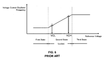
- Fig.6 shows a relationship between input (reference) voltage of the voltage control oscillator 104 and oscillation frequency which is the output signal of the voltage control oscillator 104. It is divided into three states, those are, the first state, the second state and the third state according to the voltage range of the reference voltage.
- the first state the oscillation frequency marks a point below a lower limit of the operation of the voltage control oscillator 104, and does not change (under saturation condition) as the reference voltage changes.
- the second state the oscillation frequency changes as the reference voltage.
- the oscillation frequency marks a point above an upper limit of the operation of the voltage control oscillator 104, and does not change (under saturation condition) as the reference voltage changes.
- the comparative clock can be matched to ensure a stable operation (lock) of the PLL clock signal generation circuit, which is referred to as a region capable of locking (or a lock range).
- VCL shows the reference voltage that outputs the oscillation frequency of the lower limit operation of the voltage control oscillator 104
- VCH shows the reference voltage that outputs the oscillation frequency of the upper limit operation of the voltage control oscillator 104.
- the PLL clock signal generation circuit of the prior art includes a phase comparator 11 that generates error voltage due to the phase difference, a low-pass filter 12, a voltage control oscillator 13 and a programmable N counter 14.
- This circuit uses one voltage control oscillator 13 and provides a frequency changer 15 (a 2n programmable divider is used in the following embodiment) between the one voltage control oscillator 13 and the programmable N counter 14.
- the phase comparator 11 generates error voltage according to the phase difference between the standard frequency fr and the divided frequency fv of the N division counter.
- the output error voltage from the phase comparator 11 becomes the control voltage of the voltage control oscillator 13 by cutting off the high frequency components at the low pass filter 12.
- the control voltage is provided to narrow the difference between the divided frequency fv of the oscillation frequency fs of the voltage control oscillator 13 and the standard clock fr.
- the difference between the frequency fv and the standard clock fr is zero (0)
- the circuit is under a locked condition, and the relation between the frequency fv and the standard clock fr can be expressed by the following equation (1).
- the relationship can be expressed by the equation (2).
- the region where oscillation is available in the output frequency f0 is expressed with a minimum oscillation frequency fmin and a maximum oscillation frequency fmax
- the region can be expressed in the equation (4) through (6) according to the value n of the 2N programmable divider which is a frequency changer 15.
- f0 fmin / 2 through fmax / 2 :
- n 1
- the output of the frequency changer 15 is changeable by a value of n so that a wider range of output frequency can be obtained.
- the PLL clock signal generation circuit in the prior art disclosed in the Japanese Unexamined Patent Publication No.6-326603 requires the n value of the frequency changer 15 (2N programmable divider) to be set to stretch the lock range.
- the n value should be set from the CPU which controls the PLL clock signal generation circuit and is mounted outside the PLL clock signal generation circuit.
- the clock In order to handle the change of the standard clock, the clock should be observed by the CPU and the n value should be changed according to the change of the standard clock. This increases the load to the CPU.
- the CPU process in the IC card ranges widely such as the data communication. Thus it is important to reduce the load to the CPU as much as possible.
- the circuit which observes the changes occurring at the standard clock needs to be configured.
- the objective of the present invention is to provide a PLL clock signal generation circuit that can maintain a proper locked status even when the operation region of the voltage control oscillation is narrow.
- the PLL clock signal generation circuit includes a phase comparator, a charge pump circuit, filter circuit, a voltage control oscillator, and a divider, the PLL clock signal generation circuit further including a multiple rate control circuit which outputs a control signal that changes the multiple rate so that the PLL clock signal generation circuit does not deviate from a region capable of locking when being detected of deviation from the region capable of locking by detecting a reference voltage which is an output of a filter circuit.
- the reference to the reference voltage which is an output of the filter circuit enables the detection of a state of locking of the PLL clock signal generation circuit, and also enables the change of multiple rate of the divider prior to the transition of the reference voltage to a state corresponding to a saturation of the voltage control oscillator, thereby adjusting a reference voltage to be capable of maintaining a state of locking of the PLL clock signal generation circuit.
- a PLL clock signal generation circuit is achieved that can maintain a proper state of locking even in the case when the operation region of the voltage control oscillator is narrow.
- the PLL clock signal generation circuit preferably includes a first Schmitt trigger circuit capable of detecting the multiple rate control circuit having the reference voltage higher than the upper limit value of the voltage range capable of locking, a second Schmitt trigger circuit capable of detecting the reference voltage lower than the lower limit value of the voltage range capable of locking, a D flip-flop determining that the reference voltage being higher than the upper limit value and outputting the control signal for increasing a ratio of division of the divider when the both the first Schmitt trigger circuit and the second Schmitt trigger circuit show the high level output state, and a control circuit determining that the reference voltage being lower than the lower limit value and resetting the D flip-flop when the both the first Schmitt trigger circuit and the second Schmitt trigger circuit show the low level output state.
- Such configuration of the multiple rate control circuit allows a proper and a stable detection of a state of the reference voltage and delivers a stable performance of the action and an effect of the first characteristics mentioned above.
- the PLL clock signal generation circuit preferably has each of the hysteresis width of the first Schmitt trigger circuit and the second Schmitt trigger circuit set to a value above a ripple voltage overlapping the output voltage of the charge pump circuit.
- Such configuration of the Schmitt trigger circuit allows a safer design not susceptible to the ripple voltage of the charge pump circuit.
- the present circuit An embodiment of the PLL clock signal generation circuit according to the present invention (hereinafter, referred to as "the present circuit”) will be described with reference to the drawings.
- the same reference numerals are used to refer the same circuit components of the conventional PLL clock signal generation circuit throughout the various views.
- the present circuit includes a multiple rate control circuit 107 in addition to a phase comparator 101, a charge pump circuit 102, a filter circuit 103, a voltage control oscillator 104, a first frequency divider 105 and a second frequency divider 106. All circuits, but a multiple rate control circuit 107, are the same with the corresponding circuits of the conventional PLL clock signal generation circuit shown in Fig.5.
- the multiple rate control circuit 107 is input by a reference voltage (name of the signal: LPFIN) which is an output of the filter circuit 103, and the output (name of the signal: LPFOUT) is input to the second divider 106.
- Fig. 2 shows a configuration example of a multiple rate control circuit 107.
- the multiple rate control circuit 107 includes the first Schmitt trigger circuit 201 for detecting the upper limit value of the reference voltage, the second Schmitt trigger circuit 202 for detecting the lower limit value of the reference voltage, an AND gate 203 for detecting states, a NOR gate 204 for detecting states, a D flip flop 205, and an AND gate 206 for switching a divider.
- the NOR gate 204 and the AND gate 206 allow a control circuit to reset a D flip flop 205 by determining the reference voltage being lower than the lower limit value when the state of output of both the first Schmitt trigger circuit 201 and the second Schmitt trigger circuit 202 show "L" (Low) level.
- the RESET signal which is the input signal of OR gate shown at 207 in Fig.2 is provided for setting a state of a D flip flop 205 which for switching a divider when a system reset occurred because of the application of power.
- the output from the filter circuit 103 (name of the signal: LPFIN) is input to the multiple rate control circuit 107, and the level of the reference voltage is detected at the first Schmitt trigger circuit 201 for detecting an upper limit value of the reference voltage and the second Schmitt trigger circuit 202 for detecting the lower limit value of the reference voltage.
- VCLOUT signal and VCHOUT signal are at the "H" level, a transition from the second condition to the third condition is detected, and LPFOUT signal, the output from the D flip flop 205 which is for switching the divider, is switched to the "H" (High) level.
- the multiple rate control circuit 107 uses the first Schmitt trigger circuit 201 that is adjusted to reverse the output by the voltage value VCH described in Fig. 6, thereby detecting the transition of the reference voltage from the second state to the third state. It is also necessary for the multiple rate control circuit 107 to detect the switching of the reference voltage from the second state to the first state. In this embodiment as shown in Fig. 2, the multiple rate control circuit 107 uses the second Schmitt trigger circuit 202 that is adjusted to reverse the output by the voltage value VCL described in Fig. 6.thereby detecting the transition of the reference voltage from the second state to the first state.
- the following shows a reason for the use of the Schmitt trigger circuit.
- the output voltage of the charge pump circuit 102 is overlapped with the ripple voltage.
- the Schmitt trigger circuit which has the hysteresis is suited to remove the ripple voltage.
- the value of ripple voltage is determined mostly by circuit configuration of the charge pump circuit 102.
- the width of the hysteresis needs to be set at a value above that of ripple voltage.
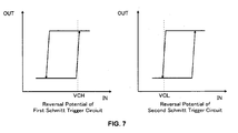
- Fig. 7 shows the hysteresis voltage setting of the first Schmitt trigger circuit 201 and the second Schmitt trigger circuit 202.
- the first Schmitt trigger circuit 201 when the hysteresis input voltage detecting VCH is above the VCH, the trigger is set to output "H", and the input voltage has hysteresis when the output returns to "L”.
- the second Schmitt trigger circuit 202 when the hysteresis input voltage detecting VCL is below the VCL, the trigger is set to output "L", and the input voltage has hysteresis when the output returns to "H”.
- Fig. 3 shows an example of a circuit configuration of the second divider 106.
- the second divider 106 includes a selector 301, a 1/2 divider 302, and a 1/48 divider 303.
- the division of the second divider 106 is configured by 5 stages of the 1/2 divider and one stage of the 1/3 divider enabling the division of the 1/96.
- the output clock (name of the signal: DIVIN) of the voltage control oscillator 104 is input to the second divider 106 where the output clock is divided.
- the output of the multiple rate control circuit 107 (name of the signal: LPFOUT) is input to the second divider 106 and is connected to the selector 301 which decides to connect the 1/2 divider 302 at the last stage to the 1/48 divider 303.
- the output of the selector 301 (name of the signal: DIVOUT) is output from the second divider 106 to be input as comparative clock together with standard clock to the phase comparator 101.
- Fig. 4 shows an example of a circuit configuration of the first divider 105.
- the first divider 105 includes a selector 301, a 1/2 divider 302 and a 1/48 divider 303.
- the division of the first divider 105 is configured by 5 stages of the 1/2 divider and one stage of the 1/3 divider enabling the division of the 1/96.
- the output clock (name of the signal: DIVIN) of the voltage control oscillator 104 is input to the first divider 105 where the output clock is divided.
- the output of the multiple rate control circuit 107 (name of the signal: LPFOUT) is input to the first divider 105 and is connected to the selector 301 which decides to connect the 1/2 divider 302 at the first stage to the 1/48 divider 303.
- the output of the 1/48 divider 303 is provided as internal clock.
- phase comparator 101 corrects the differences by increasing reference voltage to raise the oscillation frequency of the voltage control oscillator 104.
- the circuit operation including the multiple rate control circuit 107 during this process according to the present invention will be described as follows.
- the standard clock and the comparative clock which is the output frequency of the voltage control oscillator 104 divided at the second divider 106 are input to the phase comparator 101.
- the phase comparator compares the phases of the two clocks. When the phase of the comparative clock delays compared with the phase of the standard clock, the phase comparator produces UP signal by the amount equal to the phase delayed. On the contrary, when the phase of the comparative clock leads compared with the phase of the standard clock, the phase comparator produces DOWN signal by the amount equal to the phase of the leading.
- These UP signal and DOWN signal are converted to voltage through the charge pump circuit 102 and the filter circuit 103.
- the output voltage of the charge pump circuit 102 is increased by UP signal, and the output voltage of the charge pump circuit 102 is decreased by DOWN signal. This output voltage becomes reference voltage for changing the oscillation frequency of the voltage control oscillator 104.
- the reference voltage increases in the operation example of the present invention.
- the reference voltage as LPFIN signal, is input to the first Schmitt trigger circuit 201 for detecting an upper limit value of the reference voltage and the second Schmitt trigger circuit 202 for detecting a lower limit value of the reference voltage at the multiple rate control circuit 107.
- both VCHOUT that is output of the first Schmitt trigger circuit 201 for detecting the upper limit value of the reference voltage and the VCLOUT that is output of the second Schmitt trigger circuit 202 for detecting the lower limit value of the reference voltage reach the "H" level to set the LPFOUT signal that is the output of the D flip flop 205 for switching the divider to the "H" level.
- the LPFOUT signal output from the multiple rate control circuit 107 is input to the selector 301 of the second divider 106 to switch the 1/2 divider 302 that is the last stage of the second divider 106 from a state of connection to a state of bypass.
- the ratio of division of the second divider 106 is switched from 1/96 to 1/48.
- the frequency of the DIVOUT signal (comparative clock) that is output of the second divider is increased and when it reaches above the frequency of the standard clock, the output of the phase comparator 101 is changed to DOWN signal to UP signal.
- the reference voltage then decreases to lower the frequency of the voltage control oscillator 104.
- the VCHOUT signal that is output signal of the first Schmitt trigger circuit 201 reaches the "L” level (the VCLOUT signal that is the output signal of the first Schmitt trigger circuit 202 remains at the "H” level), but the output of the NOR gate 204 for detecting states does not change and LPFOUT signal stays in "H” level, and the ratio or division of the second divider 106 does not change. Therefore, the oscillation frequency of the voltage control oscillator 104 is further decreased.
- the present circuit then obtains a stable operation (a state of locking) when a phase of the frequency of the voltage control oscillator 104 x a phase of 1/48 is equal to a phase of the standard clock. This enables the circuit to correspond to a standard clock having higher frequency.
- Fig. 8 shows voltage wave forms of each signal in the above operation example (correction of the led phase).
- VCH voltage an upper limit value of the voltage range that is capable of locking
- the VCHOUT signal is changed to the "H” level.
- the output of the AND gate 203 for detecting states is switched to the "H” level and the LPFOUT signal that is output from the D flip flop 205 for switching the divider becomes "H” level.
- the LPFOUT signal switches the second divider 106 to lower the reference voltage.
- Fig. 4 shows an internal circuit of the first divider.
- the divider has a selector 301 as a corrector and corrects the internal clock at a predetermined value by bypassing a 1/2 divider 302 when the LPFOUT signal is at the "H" level.
- the following description shows a circuit operation of the present invention in which the phase of the standard clock is behind the phase of the comparative clock.
- the phase comparator 101 detects the standard clock being behind the comparative clock, and outputs DOWN signal to the charge pump circuit 102.
- the output voltage of the charge pump circuit 102 falls and the reference voltage is lowered through the filter circuit 103 to further lower the oscillation frequency of the voltage control oscillator 104.
- both output VCHOUT from the first Schmitt trigger circuit 201 for detecting the upper limit value of the reference voltage and the output VCLOUT from the second Schmitt trigger circuit 202 for detecting the lower limit value of the reference voltage are at the "L level and to set the output from the NOR gate 204 for detecting states to the "H" level and also to set the output from the AND gate 206 for detecting states to the "H" level.
- the output of the D flip flop 205 for switching the divider is reset to set the LPFOUT signal to the "L" level. This switches the second divider from a state of bypass to a state of connection.
- the LPFOUT signal is a state of the "L "
- the ratio of division of the second divider 106 is switched from 1/48 to 1/96.
- the frequency of the DIVOUT signal that is the output of the second divider is lowered and is below the frequency of the standard clock, the output of the phase comparator 101 is switched from DOWN signal to UP to increase the frequency of the voltage control oscillator 104.
- the VCLOUT signal In the case of transition from the first state to the second state, the VCLOUT signal reaches to the "H” level (the VCHOUT signal remains at the “L” level) but the output of the NOR gate 204 for detecting states does not change.
- the LPFOUT signal remains at the "L” level, and the ratio of division of the second divider 106 also remains unchanged. Therefore, the frequency of the voltage control oscillator 104 increases further.
- the PLL clock signal generation circuit thus obtains the stable operation when a phase of the frequency of the voltage control oscillator 104 x a phase of 1/96 is equal to a phase of the standard clock.
- Fig. 9 shows voltage wave forms of each signal in the above operation example (correction of the delayed phase).
- the multiple rate control circuit 107 is not limited by the circuit configuration illustrated in Fig. 2.
- the first divider 105 and the second divider 106 are also not limited by the circuit configuration illustrated in Figs. 4 and 3 respectively.
- the circuits 105 through 107 may be replaced with the other circuit configurations which can achieve circuit operations described in the above embodiment.
- the present circuit is the PLL clock signal generation circuit which includes the phase comparator, the charge pump circuit, the filter circuit, the voltage control oscillator, and the divider.
- the PLL clock signal generation circuit also includes a multiple rate control circuit which detects the state of a reference voltage which is the output from the filter circuit and changes the multiple rate according to the state of detection.
- the PLL clock signal generation circuit further detects the reference voltage in a state wherein the PLL clock signal generation circuit is out of a region capable of locking and changes the multiple rate to adjust a state to be capable of locking.
- the reference to a reference voltage allows detection of a state of locking of the PLL clock signal generation circuit, and the multiple rate can be changed before reference voltage moves into the state of saturation of the voltage control oscillator.
- a PLL clock signal generation circuit that can maintain a proper state of locking even when an operation region of the voltage control oscillator being narrow can be provided.
- the configuration of the multiple rate control circuit shown in Fig. 2 allows a relatively easy detection of a reference voltage and changes of the multiple rate. These features described above enables a configuration of the PLL clock signal generation circuit to have a wider lock range. Moreover, a hysteresis width of the first Schmitt trigger circuit and the second Schmitt trigger circuit may be set at a point above a ripple voltage value overlapping the output voltage of a charge pump circuit to design a safer configuration that is not susceptible to the ripple voltage.
Landscapes
- Stabilization Of Oscillater, Synchronisation, Frequency Synthesizers (AREA)
Applications Claiming Priority (2)
| Application Number | Priority Date | Filing Date | Title |
|---|---|---|---|
| JP2003380153A JP4546716B2 (ja) | 2003-11-10 | 2003-11-10 | Pllクロック信号生成回路 |
| JP2003380153 | 2003-11-10 |
Publications (1)
| Publication Number | Publication Date |
|---|---|
| EP1530294A1 true EP1530294A1 (de) | 2005-05-11 |
Family
ID=34431398
Family Applications (1)
| Application Number | Title | Priority Date | Filing Date |
|---|---|---|---|
| EP04256870A Withdrawn EP1530294A1 (de) | 2003-11-10 | 2004-11-05 | PLL-Taktsignalgenerator |
Country Status (4)
| Country | Link |
|---|---|
| US (1) | US7109764B2 (de) |
| EP (1) | EP1530294A1 (de) |
| JP (1) | JP4546716B2 (de) |
| CN (1) | CN100409573C (de) |
Families Citing this family (24)
| Publication number | Priority date | Publication date | Assignee | Title |
|---|---|---|---|---|
| US7305312B2 (en) * | 2005-01-10 | 2007-12-04 | Wavecrest Corporation | Method and apparatus for recording a real time signal |
| US7327172B2 (en) * | 2005-06-27 | 2008-02-05 | Lsi Corporation | Integrated clock generator with programmable spread spectrum using standard PLL circuitry |
| US7348818B2 (en) * | 2005-06-30 | 2008-03-25 | Silicon Laboratories Inc. | Tunable high-speed frequency divider |
| JP4519746B2 (ja) * | 2005-09-22 | 2010-08-04 | ローム株式会社 | クロック生成回路、およびそれを搭載した電子機器 |
| US7239188B1 (en) * | 2005-11-01 | 2007-07-03 | Integrated Device Technology, Inc. | Locked-loop integrated circuits having speed tracking circuits therein |
| JP4942990B2 (ja) * | 2005-12-12 | 2012-05-30 | パナソニック株式会社 | 半導体記憶装置 |
| US7486060B1 (en) | 2006-03-30 | 2009-02-03 | Western Digital Technologies, Inc. | Switching voltage regulator comprising a cycle comparator for dynamic voltage scaling |
| FR2900290B1 (fr) * | 2006-04-19 | 2008-11-21 | Atmel Corp | Procede et systeme pour fournir une pompe de charge pour les applications basse tension |
| US7551383B1 (en) | 2006-06-28 | 2009-06-23 | Western Digital Technologies, Inc. | Adjusting voltage delivered to disk drive circuitry based on a selected zone |
| US7495517B1 (en) * | 2006-12-14 | 2009-02-24 | Altera Corporation | Techniques for dynamically adjusting the frequency range of phase-locked loops |
| US7733189B1 (en) | 2007-09-14 | 2010-06-08 | Western Digital Technologies, Inc. | Oscillator comprising foldover detection |
| WO2009090448A2 (en) * | 2008-01-15 | 2009-07-23 | Atmel Corporation | Proportional phase comparator and method for phase-aligning digital signals |
| US8085020B1 (en) | 2008-06-13 | 2011-12-27 | Western Digital Technologies, Inc. | Switching voltage regulator employing dynamic voltage scaling with hysteretic comparator |
| JP2010135956A (ja) | 2008-12-03 | 2010-06-17 | Renesas Electronics Corp | Pll回路およびその制御方法 |
| CN101447788B (zh) * | 2008-12-16 | 2012-06-27 | 昆山锐芯微电子有限公司 | 锁相环锁定信号的产生电路 |
| CN101847215B (zh) * | 2009-03-26 | 2013-02-27 | 上海华虹集成电路有限责任公司 | 非接触式ic卡的时钟电路和数据解码电路 |
| US8559582B2 (en) * | 2010-09-13 | 2013-10-15 | Altera Corporation | Techniques for varying a periodic signal based on changes in a data rate |
| JP6871083B2 (ja) * | 2017-06-23 | 2021-05-12 | キヤノンメディカルシステムズ株式会社 | 超音波診断装置、及び消費電力低減プログラム |
| CN108362941B (zh) * | 2018-03-29 | 2023-07-18 | 珠海迈科智能科技股份有限公司 | 一种测试Tuner模组晶振频偏的设备及方法 |
| CN109150170B (zh) * | 2018-08-23 | 2021-12-31 | 豪威科技(上海)有限公司 | 锁相环电路 |
| CN111371455B (zh) * | 2019-12-31 | 2024-04-12 | 京微齐力(北京)科技有限公司 | 一种用于pll输出频率动态切换的系统 |
| FR3116353B1 (fr) * | 2020-11-16 | 2023-01-13 | St Microelectronics Rousset | Génération de signaux d'horloge |
| CN114513206A (zh) * | 2020-11-16 | 2022-05-17 | 意法半导体(鲁塞)公司 | 时钟信号生成 |
| CN116232319B (zh) * | 2023-05-08 | 2023-07-28 | 深圳市九天睿芯科技有限公司 | 锁相环、芯片及电子设备 |
Citations (3)
| Publication number | Priority date | Publication date | Assignee | Title |
|---|---|---|---|---|
| US5923196A (en) * | 1996-08-02 | 1999-07-13 | Oki Electric Industry Co., Ltd. | Band-selectable phase-locked loop |
| EP1033815A2 (de) * | 1999-03-01 | 2000-09-06 | Kabushiki Kaisha Toshiba | PLL-Schaltung |
| US20030007222A1 (en) * | 2001-07-05 | 2003-01-09 | Wataru Kwasaki | Transmission device |
Family Cites Families (24)
| Publication number | Priority date | Publication date | Assignee | Title |
|---|---|---|---|---|
| US275115A (en) * | 1883-04-03 | Abraham ayebs | ||
| JPS5354456A (en) * | 1976-10-27 | 1978-05-17 | Mitsubishi Electric Corp | Phase synchronizing oscillator |
| US4516083A (en) * | 1982-05-14 | 1985-05-07 | Motorola, Inc. | Fast lock PLL having out of lock detector control of loop filter and divider |
| US4529892A (en) * | 1982-11-23 | 1985-07-16 | Rca Corporation | Detection circuitry with multiple overlapping thresholds |
| JPS6214524A (ja) * | 1985-07-11 | 1987-01-23 | Nec Corp | 位相同期発振器 |
| JPS63226116A (ja) * | 1987-03-16 | 1988-09-20 | Hitachi Ltd | Pll回路 |
| JPH03190428A (ja) * | 1989-12-20 | 1991-08-20 | Matsushita Electric Ind Co Ltd | 位相同期回路 |
| US5140284A (en) * | 1991-02-20 | 1992-08-18 | Telefonaktiebolaget L M Ericsson | Broad band frequency synthesizer for quick frequency retuning |
| US5371480A (en) * | 1992-12-04 | 1994-12-06 | Telefonaktiebolaget L M Ericsson | Step controlled signal generator |
| US5334952A (en) * | 1993-03-29 | 1994-08-02 | Spectralink Corporation | Fast settling phase locked loop |
| JPH06326603A (ja) | 1993-05-14 | 1994-11-25 | Nippon Avionics Co Ltd | Pll周波数シンセサイザ回路 |
| JPH07212333A (ja) * | 1994-01-25 | 1995-08-11 | Alps Electric Co Ltd | 送受信機の発振回路 |
| JP3418710B2 (ja) * | 1994-03-11 | 2003-06-23 | 富士通株式会社 | 周波数誤差検出回路及びこれを用いたクロック再生回路 |
| JP3193598B2 (ja) * | 1995-08-01 | 2001-07-30 | 沖電気工業株式会社 | チャージポンプ回路およびこれを用いたpll回路 |
| JPH0983356A (ja) * | 1995-09-08 | 1997-03-28 | Kawasaki Steel Corp | クロック発生回路 |
| JPH09191247A (ja) * | 1996-01-10 | 1997-07-22 | Fujitsu General Ltd | Pll回路 |
| JPH09261042A (ja) * | 1996-03-26 | 1997-10-03 | Fujitsu Denso Ltd | 位相同期ループの引き込み方式 |
| KR100253153B1 (ko) * | 1996-12-23 | 2000-04-15 | 윤종용 | 협대역전압제어발진기를이용한광대역위상동기루프회로 |
| KR100468693B1 (ko) * | 1997-10-13 | 2005-03-16 | 삼성전자주식회사 | 안정적으로락상태를판별하는위상락검출회로 |
| US6049254A (en) * | 1997-10-16 | 2000-04-11 | Oasis Design, Inc. | Phase-locked loop which can automatically adjust to and lock upon a variable input frequency |
| US6275074B1 (en) * | 1998-01-06 | 2001-08-14 | Texas Instruments Incorporated | System for propagating a digital signal through a slew-rate limited node and method of operation |
| JP2001060870A (ja) * | 1999-08-24 | 2001-03-06 | Matsushita Electric Ind Co Ltd | 周波数シンセサイザ装置、周波数生成方法、および移動無線機 |
| JP2002009617A (ja) * | 2000-06-23 | 2002-01-11 | Murata Mfg Co Ltd | Pll回路 |
| JP3748414B2 (ja) * | 2002-02-07 | 2006-02-22 | 日本電信電話株式会社 | 位相同期ループ回路 |
-
2003
- 2003-11-10 JP JP2003380153A patent/JP4546716B2/ja not_active Expired - Fee Related
-
2004
- 2004-11-05 EP EP04256870A patent/EP1530294A1/de not_active Withdrawn
- 2004-11-09 US US10/983,649 patent/US7109764B2/en not_active Expired - Fee Related
- 2004-11-10 CN CNB200410092393XA patent/CN100409573C/zh not_active Expired - Fee Related
Patent Citations (3)
| Publication number | Priority date | Publication date | Assignee | Title |
|---|---|---|---|---|
| US5923196A (en) * | 1996-08-02 | 1999-07-13 | Oki Electric Industry Co., Ltd. | Band-selectable phase-locked loop |
| EP1033815A2 (de) * | 1999-03-01 | 2000-09-06 | Kabushiki Kaisha Toshiba | PLL-Schaltung |
| US20030007222A1 (en) * | 2001-07-05 | 2003-01-09 | Wataru Kwasaki | Transmission device |
Also Published As
| Publication number | Publication date |
|---|---|
| US7109764B2 (en) | 2006-09-19 |
| US20050099235A1 (en) | 2005-05-12 |
| JP2005143030A (ja) | 2005-06-02 |
| JP4546716B2 (ja) | 2010-09-15 |
| CN100409573C (zh) | 2008-08-06 |
| CN1617452A (zh) | 2005-05-18 |
Similar Documents
| Publication | Publication Date | Title |
|---|---|---|
| US7109764B2 (en) | PLL clock signal generation circuit | |
| US7622996B2 (en) | Multi-loop phase locked loop circuit | |
| US8264286B2 (en) | Phase-locked loop circuit | |
| JP2795323B2 (ja) | 位相差検出回路 | |
| US9160353B2 (en) | Phase frequency detector and charge pump for phase lock loop fast-locking | |
| KR20110130330A (ko) | 자기잡음제거 전압제어발진기를 이용한 주파수-위상고정루프 | |
| US6525612B2 (en) | Mode control of PLL circuit | |
| US7417477B2 (en) | PLL circuit | |
| CN112994687B (zh) | 一种参考时钟信号注入锁相环电路及消除失调方法 | |
| CN102291130A (zh) | 一种锁定精度和锁定频率均可编程的锁定检测电路 | |
| US8866556B2 (en) | Phase shift phase locked loop | |
| JP4015254B2 (ja) | ロック検出回路及びpll周波数シンセサイザ | |
| JP3840468B2 (ja) | Pll周波数シンセサイザ | |
| US7310009B2 (en) | Phase locked loop circuit having deadlock protection circuit and methods of operating same | |
| US20090179708A1 (en) | Phase lock oscillator and wireless communications device including phase lock oscillator | |
| CA2351759C (en) | Phase-locked loop | |
| CN114513204B (zh) | 一种多环路的锁相环电路及电路板组件 | |
| US20030214330A1 (en) | Phase-locked loop circuit | |
| US6894571B2 (en) | Phase locked loop circuit with selectable variable frequency dividers | |
| CN108566199B (zh) | 一种锁相环及频率控制方法 | |
| CN207782771U (zh) | 一种锁相环 | |
| CN114499503B (zh) | 一种无中断切换的锁相环电路及电路板组件 | |
| CN111817715A (zh) | 锁相方法及相关锁相环、芯片及电子装置 | |
| CN119561548B (zh) | 一种锁相环快速频率自动校准系统 | |
| JP4327144B2 (ja) | Pll回路におけるアクティブフィルタ。 |
Legal Events
| Date | Code | Title | Description |
|---|---|---|---|
| PUAI | Public reference made under article 153(3) epc to a published international application that has entered the european phase |
Free format text: ORIGINAL CODE: 0009012 |
|
| AK | Designated contracting states |
Kind code of ref document: A1 Designated state(s): AT BE BG CH CY CZ DE DK EE ES FI FR GB GR HU IE IS IT LI LU MC NL PL PT RO SE SI SK TR |
|
| AX | Request for extension of the european patent |
Extension state: AL HR LT LV MK YU |
|
| 17P | Request for examination filed |
Effective date: 20050720 |
|
| AKX | Designation fees paid |
Designated state(s): DE FR GB |
|
| 17Q | First examination report despatched |
Effective date: 20060208 |
|
| GRAP | Despatch of communication of intention to grant a patent |
Free format text: ORIGINAL CODE: EPIDOSNIGR1 |
|
| RIC1 | Information provided on ipc code assigned before grant |
Ipc: H03L 7/10 20060101ALI20150129BHEP Ipc: H03L 7/197 20060101ALI20150129BHEP Ipc: H03L 7/089 20060101AFI20150129BHEP |
|
| INTG | Intention to grant announced |
Effective date: 20150224 |
|
| STAA | Information on the status of an ep patent application or granted ep patent |
Free format text: STATUS: THE APPLICATION IS DEEMED TO BE WITHDRAWN |
|
| 18D | Application deemed to be withdrawn |
Effective date: 20150707 |