EP1530235A2 - Halbleitervorrichtung - Google Patents
Halbleitervorrichtung Download PDFInfo
- Publication number
- EP1530235A2 EP1530235A2 EP04026060A EP04026060A EP1530235A2 EP 1530235 A2 EP1530235 A2 EP 1530235A2 EP 04026060 A EP04026060 A EP 04026060A EP 04026060 A EP04026060 A EP 04026060A EP 1530235 A2 EP1530235 A2 EP 1530235A2
- Authority
- EP
- European Patent Office
- Prior art keywords
- metal conductor
- semiconductor device
- external electrode
- heat spreader
- radiation member
- Prior art date
- Legal status (The legal status is an assumption and is not a legal conclusion. Google has not performed a legal analysis and makes no representation as to the accuracy of the status listed.)
- Withdrawn
Links
Images


Classifications
-
- H—ELECTRICITY
- H10—SEMICONDUCTOR DEVICES; ELECTRIC SOLID-STATE DEVICES NOT OTHERWISE PROVIDED FOR
- H10W—GENERIC PACKAGES, INTERCONNECTIONS, CONNECTORS OR OTHER CONSTRUCTIONAL DETAILS OF DEVICES COVERED BY CLASS H10
- H10W72/00—Interconnections or connectors in packages
-
- H—ELECTRICITY
- H10—SEMICONDUCTOR DEVICES; ELECTRIC SOLID-STATE DEVICES NOT OTHERWISE PROVIDED FOR
- H10W—GENERIC PACKAGES, INTERCONNECTIONS, CONNECTORS OR OTHER CONSTRUCTIONAL DETAILS OF DEVICES COVERED BY CLASS H10
- H10W90/00—Package configurations
-
- H—ELECTRICITY
- H10—SEMICONDUCTOR DEVICES; ELECTRIC SOLID-STATE DEVICES NOT OTHERWISE PROVIDED FOR
- H10W—GENERIC PACKAGES, INTERCONNECTIONS, CONNECTORS OR OTHER CONSTRUCTIONAL DETAILS OF DEVICES COVERED BY CLASS H10
- H10W40/00—Arrangements for thermal protection or thermal control
- H10W40/10—Arrangements for heating
-
- H—ELECTRICITY
- H10—SEMICONDUCTOR DEVICES; ELECTRIC SOLID-STATE DEVICES NOT OTHERWISE PROVIDED FOR
- H10W—GENERIC PACKAGES, INTERCONNECTIONS, CONNECTORS OR OTHER CONSTRUCTIONAL DETAILS OF DEVICES COVERED BY CLASS H10
- H10W90/00—Package configurations
- H10W90/701—Package configurations characterised by the relative positions of pads or connectors relative to package parts
- H10W90/751—Package configurations characterised by the relative positions of pads or connectors relative to package parts of bond wires
- H10W90/756—Package configurations characterised by the relative positions of pads or connectors relative to package parts of bond wires between a chip and a stacked lead frame, conducting package substrate or heat sink
Definitions
- the present invention relates to a semiconductor apparatus in which a main current of a semiconductor device flows on the wiring pattern formed on an insulation board.
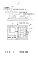
- a heat spreader 14 is soldered to a copper pattern 13 formed on an insulation circuit board 12, and a semiconductor chip 15 is loaded on to the heat spreader 14.
- An end of an external electrode 17 is soldered to the copper pattern 13, and the external electrode 17 and an external electrode S 18 are insulated by an insulator 19.
- a drain current from the external electrode 17 flows through the copper pattern 13, passes through the heat spreader 14, and enters the drain electrode of the semiconductor chip 15.
- the constraint of the bonding operation can possibly require a predetermined distance between the external electrode 18 and the semiconductor chip 15.
- the copper pattern 13 is thin (for example, about 0.07 mm) , the heating value of the copper pattern 13 becomes large due to the current flowing through the copper pattern 13 when the distance between the external electrode 17 and the semiconductor chip 15, that is, the wiring length, becomes longer.
- the width (vertical length indicated by the arrow shown in FIG. 1) of the copper pattern 13 has been increased to get a larger cross-sectional area as shown in the figure (top perspective view) of the semiconductor module 11 shown in FIG. 1. That is, the width in the direction normal to the direction of the flow of the drain current is increased to obtain a larger cross-sectional area of the current path of the drain current.
- FIG. 2 shows the structure of another semiconductor module 21 in which the heat of the copper pattern 13 due to the main current is suppressed.
- an external electrode 22 is extended to the position below the semiconductor chip 15.
- the dimension of the side opposite the semiconductor chip 15 of the external electrode 22 is longer, and the semiconductor chip 15 is fixed to it by solder, etc.
- the drain current flowing from the external electrode 22 enters the drain electrode of the semiconductor chip 15 from the external electrode 22 below the semiconductor chip 15. Since the external electrode 22 can be thicker than the copper pattern 13, the cross-sectional area of the current path can be increased by the above-mentioned structure, thereby suppressing the heat of the copper pattern 13.
- the patent literature 1 discloses the structure of providing a metal frame 2 in which a semiconductor device loaded unit 2a and a main electrode terminal 2b are incorporated into one unit, a semiconductor device 4 is soldered to the semiconductor device loaded unit 2a, and the main electrode terminal 2b is bent and led outside.
- the invention described in the patent literature 1 also has the main current flowing through the metal frame 2, thereby also suppressing the heat of the conductor pattern formed on the insulation board.
- Patent Literature 1 Japanese Patent Publication No. Hei 8-17188 (FIG. 1)
- the width of the copper pattern 13 can be smaller, but it is necessary to increase the outer dimensions of the external electrode 22 formed by copper, etc. so that the entire semiconductor chip 15 can be loaded. As a result, there is the problem that the cost of parts becomes higher.
- the present invention aims at suppressing the rise in temperature of the wiring pattern in which a main current flows, and reducing the cost of parts.
- the semiconductor apparatus includes: a semiconductor device; a metal conductor forming an external terminal through which a main current of the semiconductor device flows; and a conductive wiring pattern, formed on an insulation board, for electrically connecting the metal conductor to the semiconductor device.
- the metal conductor and the semiconductor device are arranged such that the wiring length of the wiring pattern functioning as a current path between the metal conductor and the semiconductor device can be short.
- the wiring length of the wiring pattern between the metal conductor and the semiconductor device can be shortened, and the heat of the wiring pattern through which the main current of the semiconductor device flows can be reduced without increasing the outer dimensions of the semiconductor apparatus.
- Another semiconductor apparatus includes: a semiconductor device; a metal conductor forming an external terminal through which a main current of the semiconductor device flows; a radiation member loaded with the semiconductor device; and a conductive wiring pattern, formed on a radiation member loaded with the semiconductor device and an insulation board, for electrically connecting the metal conductor to the radiation member.
- the metal conductor and the radiation member are arranged such that the wiring length of the wiring pattern functioning as the current path between the metal conductor and the radiation member can be short.
- the wiring length of the wiring pattern between the radiation member and the metal conductor can be shortened, and the rise in temperature of the wiring pattern through which a main current flows can be reduced without increasing the outer dimensions of the semiconductor apparatus.
- the space between the side of the metal conductor and the side of the semiconductor device or the radiation member is filled with a conductive material to reduce the resistance between the metal conductor and the semiconductor device or the radiation member.
- the resistance between the metal conductor and the radiation member can be reduced.
- the current flowing through the wiring pattern can be decreased, the rise in temperature can be suppressed and the outer dimensions of the semiconductor apparatus can be reduced.
- the conductive material is solder, and a resist is applied to prevent a solder layer from being formed on the top of the sides of the metal conductor and the semiconductor device or the radiation member.
- the solder when the space between the metal conductor and the semiconductor device or the radiation member is filled with solder, the solder can be prevented from covering the top of the metal conductor of the radiation member (or the semiconductor device). Thus, the insulation distance between the soldered portion and a portion having different polarity can be reserved.
- the metal conductor includes: a first metal conductor connected to the semiconductor device by wire bonding; and a second metal conductor electrically connected to the radiation member by the wiring pattern.
- the end portion of the second metal conductor is protruded farther than the end portion of the first metal conductor toward the semiconductor device, and the distance between the end portion of the second metal conductor and the semiconductor device or the radiation member is shortened.
- a predetermined distance can be reserved between the first metal conductor and the semiconductor device for the wire bonding operation, and the distance between the second metal conductor and the semiconductor device or the radiation member can be shortened.
- the rise in temperature can be suppressed, and the outer dimensions of the semiconductor apparatus can be reduced.
- the first metal conductor corresponds to an external electrode 37 shown in FIG. 3
- the second metal conductor corresponds to an external electrode 52 shown in FIG. 3.
- FIG. 3 is a schematic sectional view of a power semiconductor module (semiconductor apparatus) 31.
- a copper pattern (conductive wiring pattern) 33 is formed on an insulation circuit board 32.
- a heat spreader (radiation member) 34 is soldered to the copper pattern 33.
- a semiconductor chip (semiconductor device) 35 is loaded on to the heat spreader 34, and the drain electrode of the semiconductor chip 35 is electrically connected to the heat spreader 34.
- the heat spreader 34 is provided for the radiation of the semiconductor chip 35.
- an external electrode D metal conductor or a metal wiring conductor
- a semiconductor module the power semiconductor module
- One end of an external electrode 37 is connected to the source electrode of the semiconductor chip 35 by wire bonding, and the other end is led outside the case to form an external terminal.
- the external electrode 36 and the external electrode 37 are inserted into the resin, and are insulated by an insulator 38.
- a resin case is covered on the insulation circuit board 32 loaded with the semiconductor chip 35, and the case is adhered to the insulation circuit board 32 to form the semiconductor module 31.
- the external electrode 36 and the heat spreader 34 are arranged such that the distance a (distance a in the horizontal direction shown in FIG. 3) between a side 36a of the external electrode 36 and a side 34a of the heat spreader 34 can be short when, for example, there is a small constraint by an operation such as wire bonding, etc.
- the wiring length (distance a) of the copper pattern 33 between the external electrode 36 and the heat spreader 34 is short. Therefore, the resistance of the copper pattern 33 between the external electrode 36 and the heat spreader 34 can be small. Thus, the rise in temperature of the copper pattern 33 when a drain current flows can be suppressed. Furthermore, by shortening the wiring length of the copper pattern 33 between the external electrode 36 and the heat spreader 34, it is not necessary to increase the width (length in the direction normal to the direction of the drain current) of the copper pattern 33, thereby reducing the outer dimensions of the semiconductor module 31.
- FIG. 4 is a schematic cross-sectional view of a semiconductor module 41 according to the second embodiment of the present invention.
- the same unit shown in FIG. 3 is assigned the same reference numeral, and the explanation is omitted here.
- the space between the side 36a of the external electrode 36 and the side 34a of the heat spreader 34 is filled with solder (conductive material) 42 to reduce the resistance between the external electrode 36 and the heat spreader 34.
- the drain current entering from the external electrode 36 flows into the heat spreader 34 through the copper pattern 33 and the solder 42.
- the thickness (dimension in the vertical direction shown in FIG. 4)) of the solder 42 is larger than that of the copper pattern 33. Therefore, most of the drain current passes through the solder 42 to the heat spreader 34. Furthermore, it enters the drain electrode of the semiconductor chip 35 through the heat spreader 34. Thus, the drain current flowing through the copper pattern 33 between the external electrode 36 and the heat spreader 34 decreases, thereby suppressing the rise in temperature of the copper pattern 33.
- the space between the external electrode 36 and the heat spreader 34 is filled with the solder 42 to increase the cross-sectional area of the current path of the drain current flowing from the external electrode 36 to the heat spreader 34.
- the current which flows through the portion of the solder 42 can be increased, and the current which flows through the copper pattern 33 between the external electrode 36 and the heat spreader 34 can be reduced.
- the rise in temperature of the copper pattern 33 can be suppressed.
- solder 42 When the space between the external electrode 36 and the heat spreader 34 is filled with the solder 42, metal plating is applied to the side 36a of the external electrode 36 and the side 34a of the heat spreader 34, and a solder resist can be applied to the top of either side.
- the solder 42 can be prevented from reaching upper portion of the external electrode 37 or the top of the heat spreader 34 when the space between the external electrode 36 and the heat spreader 34 is filled with the solder.
- FIG. 5 is a schematic cross-sectional view of a semiconductor module 51 according to the third embodiment of the present invention.
- the same unit shown in FIG. 3 is assigned the same reference numeral, and the explanation is omitted here.
- an end portion 52b of the external electrode 52 is protruded toward the heat spreader 34 to shorten the distance a between the side 52a of the external electrode 52 and the side 34a of the heat spreader 34.
- the tip of the end portion 52b of the external electrode 52 is protruded farther than the tip of an end portion 37a of the external electrode 37 toward the semiconductor chip 35 (to the right in the horizontal direction as viewed from the front shown in FIG. 5).
- a predetermined distance is reserved between the end portion 37a of the external electrode 37 and the end portion of the semiconductor chip 35 where wire bonding 53 is performed, thereby shortening the distance a between the side 52a of the external electrode 52 and the side 34a of the heat spreader 34.
- the dimension in the horizontal direction of the end portion 52b of the lower external electrode 52 is increased, and the dimension of the upper 37 is shorter. Therefore, the distance between the external electrode 37 and the semiconductor chip 15 can be sufficiently reserved when the wire bonding 53 is performed between the semiconductor chip 35 and the end portion 37a of the upper external electrode 37.
- the distance between the external electrode 52 and the heat spreader 34 through which a drain current flows can be shortened.
- a predetermined distance can be reserved between the external electrode 37 and the semiconductor chip 35, and the distance between the external electrode 52 and the heat spreader 34 in which a main current flows can be shortened.
- the resistance of the copper pattern 33 between the external electrode 37 and the heat spreader 34 can be reduced, and the rise in temperature of the copper pattern 33 can be suppressed.
- the distance between the external electrode 36 and the heat spreader 34 can also be shortened, and it is not necessary to increase the width (length in the direction normal to the flow direction of a current) of the copper pattern 33, the outer dimensions of the semiconductor module 41 can be reduced.
- the solder 42 can fill the space between the external electrode 52 and the heat spreader 34.
- the cross-sectional area of the current path between the external electrode 52 and the heat spreader 34 can be increased, thereby further reducing the resistance.
- the present invention is not limited to the above-mentioned embodiments, but can also be configured as follows.
- the heat spreader 34 is provided for the radiation of the semiconductor chip 35. It can be replaced with the semiconductor chip 35 directly soldered onto the copper pattern 33. In this case, the distance between the side of the semiconductor chip 35 and the side of the external electrode 36 or 52 is to be shortened
- the material for filling the space between the 36 and the heat spreader 34 is not limited to the solder 42, but any conductive material for connecting with low resistance between the external electrode 36 of copper and the heat spreader 34 or semiconductor chip 35 can be applied.
- the resist to be applied to the sides of the external electrode 36 and the heat spreader 34 is not limited to a solder resist, but any resist can be applied depending on an available conductive material.
- the wiring length of the wiring pattern between a metal conductor and a semiconductor device or a radiation member can be shortened. Therefore, the rise in temperature of the wiring pattern can be suppressed, and the outer dimensions of the semiconductor apparatus can be reduced. Additionally, by filling the space between the metal conductor and the semiconductor device or the radiation member with a conductive material, the resistance between the metal conductor and the semiconductor device or the radiation member can be reduced, the rise in temperature of the wiring pattern can be suppressed, and the outer dimensions of the semiconductor apparatus can be decreased.
- a semiconductor apparatus in which a main current of a semiconductor device flows through a wiring pattern formed on an insulation circuit board, the rise in temperature of the wiring pattern is suppressed and the increase in cost of parts can be minimized.
- a copper pattern is formed on the insulation circuit board.
- a heat spreader is soldered to the copper pattern, and the heat spreader is loaded with a semiconductor chip.
- An external electrode and the heat spreader are arranged to shorten the distance between the side of the external electrode and the side of the heat spreader.
Landscapes
- Cooling Or The Like Of Semiconductors Or Solid State Devices (AREA)
Applications Claiming Priority (2)
| Application Number | Priority Date | Filing Date | Title |
|---|---|---|---|
| JP2003374116A JP2005142189A (ja) | 2003-11-04 | 2003-11-04 | 半導体装置 |
| JP2003374116 | 2003-11-04 |
Publications (1)
| Publication Number | Publication Date |
|---|---|
| EP1530235A2 true EP1530235A2 (de) | 2005-05-11 |
Family
ID=34431251
Family Applications (1)
| Application Number | Title | Priority Date | Filing Date |
|---|---|---|---|
| EP04026060A Withdrawn EP1530235A2 (de) | 2003-11-04 | 2004-11-03 | Halbleitervorrichtung |
Country Status (6)
| Country | Link |
|---|---|
| US (1) | US7256489B2 (de) |
| EP (1) | EP1530235A2 (de) |
| JP (1) | JP2005142189A (de) |
| KR (1) | KR100773289B1 (de) |
| CN (1) | CN100345290C (de) |
| TW (1) | TWI255542B (de) |
Families Citing this family (14)
| Publication number | Priority date | Publication date | Assignee | Title |
|---|---|---|---|---|
| JPWO2007026944A1 (ja) * | 2005-08-31 | 2009-03-12 | 三洋電機株式会社 | 回路装置およびその製造方法 |
| JP4238864B2 (ja) * | 2005-11-02 | 2009-03-18 | ソニー株式会社 | 半導体装置および半導体装置の製造方法 |
| JP2007335632A (ja) * | 2006-06-15 | 2007-12-27 | Toyota Industries Corp | 半導体装置 |
| US8076696B2 (en) * | 2009-10-30 | 2011-12-13 | General Electric Company | Power module assembly with reduced inductance |
| JP5747737B2 (ja) * | 2011-08-26 | 2015-07-15 | 三菱電機株式会社 | 半導体装置とその製造方法 |
| DE112011105612B4 (de) * | 2011-09-13 | 2014-12-31 | Toyota Jidosha Kabushiki Kaisha | Halbleitermodul |
| JP5637156B2 (ja) * | 2012-02-22 | 2014-12-10 | トヨタ自動車株式会社 | 半導体モジュール |
| EP2833405A4 (de) | 2012-03-28 | 2016-01-13 | Fuji Electric Co Ltd | Halbleiterbauelement und herstellungsverfahren für das halbleiterbauelement |
| JP5831626B2 (ja) | 2012-03-28 | 2015-12-09 | 富士電機株式会社 | 半導体装置及び半導体装置の製造方法 |
| CN104170085B (zh) * | 2012-03-28 | 2017-05-10 | 富士电机株式会社 | 半导体装置 |
| US9391055B2 (en) | 2012-12-05 | 2016-07-12 | Lockheed Martin Corporation | Power module having stacked substrates arranged to provide tightly-coupled source and return current paths |
| JP6044321B2 (ja) * | 2012-12-19 | 2016-12-14 | 富士電機株式会社 | 半導体モジュール |
| JP6171586B2 (ja) | 2013-06-04 | 2017-08-02 | 富士電機株式会社 | 半導体装置 |
| EP3217430B1 (de) * | 2014-11-06 | 2021-12-29 | Mitsubishi Electric Corporation | Halbleitermodul mit einem leitfähigen element und einem lötstopplack |
Family Cites Families (14)
| Publication number | Priority date | Publication date | Assignee | Title |
|---|---|---|---|---|
| JPS60154547A (ja) | 1984-01-24 | 1985-08-14 | Nec Corp | 半導体装置 |
| JPH0817188B2 (ja) | 1989-05-22 | 1996-02-21 | 富士電機株式会社 | 半導体装置 |
| JP2772184B2 (ja) * | 1991-11-07 | 1998-07-02 | 株式会社東芝 | 半導体装置 |
| JPH06275926A (ja) | 1993-03-18 | 1994-09-30 | Mitsubishi Electric Corp | 高周波混成集積回路装置 |
| JP3096536B2 (ja) * | 1993-03-25 | 2000-10-10 | 三洋電機株式会社 | 混成集積回路 |
| US5559374A (en) * | 1993-03-25 | 1996-09-24 | Sanyo Electric Co., Ltd. | Hybrid integrated circuit |
| JP3414017B2 (ja) * | 1994-12-09 | 2003-06-09 | ソニー株式会社 | 半導体装置 |
| JP3847807B2 (ja) | 1995-01-30 | 2006-11-22 | 財団法人国際科学振興財団 | 半導体装置 |
| JP3396566B2 (ja) * | 1995-10-25 | 2003-04-14 | 三菱電機株式会社 | 半導体装置 |
| JPH09148523A (ja) * | 1995-11-21 | 1997-06-06 | Toshiba Corp | 半導体装置 |
| JP3665426B2 (ja) | 1996-07-17 | 2005-06-29 | 東芝マイクロエレクトロニクス株式会社 | 半導体装置の製造方法 |
| JPH1187575A (ja) * | 1997-09-11 | 1999-03-30 | Fuji Electric Co Ltd | 半導体装置 |
| JP3828036B2 (ja) * | 2002-03-28 | 2006-09-27 | 三菱電機株式会社 | 樹脂モールド型デバイスの製造方法及び製造装置 |
| JP3958156B2 (ja) * | 2002-08-30 | 2007-08-15 | 三菱電機株式会社 | 電力用半導体装置 |
-
2003
- 2003-11-04 JP JP2003374116A patent/JP2005142189A/ja active Pending
-
2004
- 2004-11-02 US US10/979,563 patent/US7256489B2/en not_active Expired - Fee Related
- 2004-11-02 KR KR1020040088136A patent/KR100773289B1/ko not_active Expired - Fee Related
- 2004-11-02 TW TW093133288A patent/TWI255542B/zh not_active IP Right Cessation
- 2004-11-03 EP EP04026060A patent/EP1530235A2/de not_active Withdrawn
- 2004-11-03 CN CNB2004100883788A patent/CN100345290C/zh not_active Expired - Fee Related
Also Published As
| Publication number | Publication date |
|---|---|
| KR20050042724A (ko) | 2005-05-10 |
| TWI255542B (en) | 2006-05-21 |
| KR100773289B1 (ko) | 2007-11-05 |
| TW200524137A (en) | 2005-07-16 |
| CN1614773A (zh) | 2005-05-11 |
| US7256489B2 (en) | 2007-08-14 |
| US20050093137A1 (en) | 2005-05-05 |
| CN100345290C (zh) | 2007-10-24 |
| JP2005142189A (ja) | 2005-06-02 |
Similar Documents
| Publication | Publication Date | Title |
|---|---|---|
| US6423623B1 (en) | Low Resistance package for semiconductor devices | |
| US10347567B2 (en) | Semiconductor device and method of manufacturing the same | |
| US6225694B1 (en) | Semiconductor device | |
| US7256489B2 (en) | Semiconductor apparatus | |
| US9370113B2 (en) | Power semiconductor module with current sensor | |
| EP0700086A2 (de) | Integrierte Schaltungspackung mit verbesserter Wärmesenke | |
| US20110233759A1 (en) | Semiconductor device | |
| US8963303B2 (en) | Power electronic device | |
| US20090051022A1 (en) | Lead frame structure | |
| US9924594B2 (en) | Power semiconductor module and method for producing a power semiconductor module | |
| US7298034B2 (en) | Multi-chip semiconductor connector assemblies | |
| JP2004519849A (ja) | 電源モジュール装置と支持手段上に搭載される集積回路とを備える装置 | |
| US20180301398A1 (en) | SMD Package | |
| CN108987368B (zh) | 具有由钢制成的绝缘金属基板的印刷电路板 | |
| US6664629B2 (en) | Semiconductor device | |
| US12582016B2 (en) | Semiconductor device | |
| KR100788858B1 (ko) | 집적 회로 패키지의 구조물 및 어셈블리 방법 | |
| NL2018505B1 (en) | Semiconductor device | |
| US11631622B2 (en) | Semiconductor device and semiconductor device manufacturing method | |
| US20240106196A1 (en) | Semiconductor light emitting device | |
| US11212908B2 (en) | Semiconductor apparatus | |
| CN100378980C (zh) | 半导体装置 | |
| JP3172393B2 (ja) | 混成集積回路装置 | |
| US20050206013A1 (en) | Chip module | |
| JP2008041566A (ja) | 半導体装置およびその製造方法 |
Legal Events
| Date | Code | Title | Description |
|---|---|---|---|
| PUAI | Public reference made under article 153(3) epc to a published international application that has entered the european phase |
Free format text: ORIGINAL CODE: 0009012 |
|
| 17P | Request for examination filed |
Effective date: 20041103 |
|
| AK | Designated contracting states |
Kind code of ref document: A2 Designated state(s): AT BE BG CH CY CZ DE DK EE ES FI FR GB GR HU IE IS IT LI LU MC NL PL PT RO SE SI SK TR |
|
| AX | Request for extension of the european patent |
Extension state: AL HR LT LV MK YU |
|
| STAA | Information on the status of an ep patent application or granted ep patent |
Free format text: STATUS: THE APPLICATION HAS BEEN WITHDRAWN |
|
| 18W | Application withdrawn |
Effective date: 20100316 |