EP1528674B1 - Filtre à résonateurs à ondes acoustiques de volume empilés avec largeur de bande passante contrôlable - Google Patents
Filtre à résonateurs à ondes acoustiques de volume empilés avec largeur de bande passante contrôlable Download PDFInfo
- Publication number
- EP1528674B1 EP1528674B1 EP04014569A EP04014569A EP1528674B1 EP 1528674 B1 EP1528674 B1 EP 1528674B1 EP 04014569 A EP04014569 A EP 04014569A EP 04014569 A EP04014569 A EP 04014569A EP 1528674 B1 EP1528674 B1 EP 1528674B1
- Authority
- EP
- European Patent Office
- Prior art keywords
- acoustic
- band
- fbars
- pass filter
- layer
- Prior art date
- Legal status (The legal status is an assumption and is not a legal conclusion. Google has not performed a legal analysis and makes no representation as to the accuracy of the status listed.)
- Expired - Fee Related
Links
- 239000000463 material Substances 0.000 claims description 139
- 239000004642 Polyimide Substances 0.000 claims description 16
- 238000000034 method Methods 0.000 claims description 16
- 229920001721 polyimide Polymers 0.000 claims description 16
- 238000004519 manufacturing process Methods 0.000 claims description 10
- 239000004033 plastic Substances 0.000 claims description 9
- 229920000052 poly(p-xylylene) Polymers 0.000 claims description 8
- 238000004528 spin coating Methods 0.000 claims description 7
- 238000001914 filtration Methods 0.000 claims description 6
- -1 poly(para-xylylene) Polymers 0.000 claims description 4
- 238000000151 deposition Methods 0.000 claims description 3
- 239000010410 layer Substances 0.000 description 105
- 229910052751 metal Inorganic materials 0.000 description 22
- 239000002184 metal Substances 0.000 description 22
- ZOKXTWBITQBERF-UHFFFAOYSA-N Molybdenum Chemical compound [Mo] ZOKXTWBITQBERF-UHFFFAOYSA-N 0.000 description 15
- 229910052750 molybdenum Inorganic materials 0.000 description 15
- 239000011733 molybdenum Substances 0.000 description 15
- VYPSYNLAJGMNEJ-UHFFFAOYSA-N Silicium dioxide Chemical compound O=[Si]=O VYPSYNLAJGMNEJ-UHFFFAOYSA-N 0.000 description 14
- 230000008878 coupling Effects 0.000 description 12
- 238000010168 coupling process Methods 0.000 description 12
- 238000005859 coupling reaction Methods 0.000 description 12
- 238000004544 sputter deposition Methods 0.000 description 12
- 239000000758 substrate Substances 0.000 description 10
- 238000001312 dry etching Methods 0.000 description 8
- 239000000377 silicon dioxide Substances 0.000 description 7
- KWYUFKZDYYNOTN-UHFFFAOYSA-M Potassium hydroxide Chemical compound [OH-].[K+] KWYUFKZDYYNOTN-UHFFFAOYSA-M 0.000 description 6
- 239000010408 film Substances 0.000 description 6
- 239000003870 refractory metal Substances 0.000 description 6
- XLOMVQKBTHCTTD-UHFFFAOYSA-N Zinc monoxide Chemical compound [Zn]=O XLOMVQKBTHCTTD-UHFFFAOYSA-N 0.000 description 4
- PMHQVHHXPFUNSP-UHFFFAOYSA-M copper(1+);methylsulfanylmethane;bromide Chemical compound Br[Cu].CSC PMHQVHHXPFUNSP-UHFFFAOYSA-M 0.000 description 4
- 238000003780 insertion Methods 0.000 description 4
- 230000037431 insertion Effects 0.000 description 4
- 239000005360 phosphosilicate glass Substances 0.000 description 4
- 239000010409 thin film Substances 0.000 description 4
- 230000015556 catabolic process Effects 0.000 description 3
- 230000001413 cellular effect Effects 0.000 description 3
- 238000006731 degradation reaction Methods 0.000 description 3
- 238000002955 isolation Methods 0.000 description 3
- ZAMOUSCENKQFHK-UHFFFAOYSA-N Chlorine atom Chemical compound [Cl] ZAMOUSCENKQFHK-UHFFFAOYSA-N 0.000 description 2
- KRHYYFGTRYWZRS-UHFFFAOYSA-N Fluorane Chemical compound F KRHYYFGTRYWZRS-UHFFFAOYSA-N 0.000 description 2
- GWEVSGVZZGPLCZ-UHFFFAOYSA-N Titan oxide Chemical compound O=[Ti]=O GWEVSGVZZGPLCZ-UHFFFAOYSA-N 0.000 description 2
- 239000000460 chlorine Substances 0.000 description 2
- 229910052801 chlorine Inorganic materials 0.000 description 2
- 239000000470 constituent Substances 0.000 description 2
- 230000008021 deposition Effects 0.000 description 2
- 238000005530 etching Methods 0.000 description 2
- 230000001788 irregular Effects 0.000 description 2
- HFGPZNIAWCZYJU-UHFFFAOYSA-N lead zirconate titanate Chemical compound [O-2].[O-2].[O-2].[O-2].[O-2].[Ti+4].[Zr+4].[Pb+2] HFGPZNIAWCZYJU-UHFFFAOYSA-N 0.000 description 2
- 238000004518 low pressure chemical vapour deposition Methods 0.000 description 2
- 239000002861 polymer material Substances 0.000 description 2
- 239000000725 suspension Substances 0.000 description 2
- 238000001771 vacuum deposition Methods 0.000 description 2
- 238000001039 wet etching Methods 0.000 description 2
- 239000011787 zinc oxide Substances 0.000 description 2
- RTAQQCXQSZGOHL-UHFFFAOYSA-N Titanium Chemical compound [Ti] RTAQQCXQSZGOHL-UHFFFAOYSA-N 0.000 description 1
- 230000005540 biological transmission Effects 0.000 description 1
- 238000005137 deposition process Methods 0.000 description 1
- 239000000539 dimer Substances 0.000 description 1
- 239000007772 electrode material Substances 0.000 description 1
- 238000001704 evaporation Methods 0.000 description 1
- 230000008020 evaporation Effects 0.000 description 1
- PCHJSUWPFVWCPO-UHFFFAOYSA-N gold Chemical compound [Au] PCHJSUWPFVWCPO-UHFFFAOYSA-N 0.000 description 1
- 239000010931 gold Substances 0.000 description 1
- 229910052737 gold Inorganic materials 0.000 description 1
- ORUIBWPALBXDOA-UHFFFAOYSA-L magnesium fluoride Chemical compound [F-].[F-].[Mg+2] ORUIBWPALBXDOA-UHFFFAOYSA-L 0.000 description 1
- 229910001635 magnesium fluoride Inorganic materials 0.000 description 1
- 229910021421 monocrystalline silicon Inorganic materials 0.000 description 1
- 229910052758 niobium Inorganic materials 0.000 description 1
- 239000010955 niobium Substances 0.000 description 1
- GUCVJGMIXFAOAE-UHFFFAOYSA-N niobium atom Chemical compound [Nb] GUCVJGMIXFAOAE-UHFFFAOYSA-N 0.000 description 1
- 239000002245 particle Substances 0.000 description 1
- 238000000059 patterning Methods 0.000 description 1
- 238000000206 photolithography Methods 0.000 description 1
- 229920002120 photoresistant polymer Polymers 0.000 description 1
- 229920003223 poly(pyromellitimide-1,4-diphenyl ether) Polymers 0.000 description 1
- 229920000642 polymer Polymers 0.000 description 1
- 239000002243 precursor Substances 0.000 description 1
- 239000011241 protective layer Substances 0.000 description 1
- 235000012239 silicon dioxide Nutrition 0.000 description 1
- 239000010936 titanium Substances 0.000 description 1
- 229910052719 titanium Inorganic materials 0.000 description 1
- 239000004408 titanium dioxide Substances 0.000 description 1
- WFKWXMTUELFFGS-UHFFFAOYSA-N tungsten Chemical compound [W] WFKWXMTUELFFGS-UHFFFAOYSA-N 0.000 description 1
- 229910052721 tungsten Inorganic materials 0.000 description 1
- 239000010937 tungsten Substances 0.000 description 1
Images


Classifications
-
- H—ELECTRICITY
- H03—ELECTRONIC CIRCUITRY
- H03H—IMPEDANCE NETWORKS, e.g. RESONANT CIRCUITS; RESONATORS
- H03H9/00—Networks comprising electromechanical or electro-acoustic devices; Electromechanical resonators
- H03H9/46—Filters
- H03H9/54—Filters comprising resonators of piezo-electric or electrostrictive material
- H03H9/58—Multiple crystal filters
- H03H9/582—Multiple crystal filters implemented with thin-film techniques
- H03H9/586—Means for mounting to a substrate, i.e. means constituting the material interface confining the waves to a volume
- H03H9/587—Air-gaps
-
- H—ELECTRICITY
- H03—ELECTRONIC CIRCUITRY
- H03H—IMPEDANCE NETWORKS, e.g. RESONANT CIRCUITS; RESONATORS
- H03H9/00—Networks comprising electromechanical or electro-acoustic devices; Electromechanical resonators
- H03H9/02—Details
- H03H9/125—Driving means, e.g. electrodes, coils
- H03H9/13—Driving means, e.g. electrodes, coils for networks consisting of piezoelectric or electrostrictive materials
- H03H9/132—Driving means, e.g. electrodes, coils for networks consisting of piezoelectric or electrostrictive materials characterized by a particular shape
-
- H—ELECTRICITY
- H03—ELECTRONIC CIRCUITRY
- H03H—IMPEDANCE NETWORKS, e.g. RESONANT CIRCUITS; RESONATORS
- H03H9/00—Networks comprising electromechanical or electro-acoustic devices; Electromechanical resonators
- H03H9/46—Filters
- H03H9/54—Filters comprising resonators of piezo-electric or electrostrictive material
- H03H9/58—Multiple crystal filters
- H03H9/582—Multiple crystal filters implemented with thin-film techniques
- H03H9/583—Multiple crystal filters implemented with thin-film techniques comprising a plurality of piezoelectric layers acoustically coupled
- H03H9/584—Coupled Resonator Filters [CFR]
-
- H—ELECTRICITY
- H03—ELECTRONIC CIRCUITRY
- H03H—IMPEDANCE NETWORKS, e.g. RESONANT CIRCUITS; RESONATORS
- H03H9/00—Networks comprising electromechanical or electro-acoustic devices; Electromechanical resonators
- H03H9/46—Filters
- H03H9/54—Filters comprising resonators of piezo-electric or electrostrictive material
- H03H9/58—Multiple crystal filters
- H03H9/60—Electric coupling means therefor
- H03H9/605—Electric coupling means therefor consisting of a ladder configuration
-
- Y—GENERAL TAGGING OF NEW TECHNOLOGICAL DEVELOPMENTS; GENERAL TAGGING OF CROSS-SECTIONAL TECHNOLOGIES SPANNING OVER SEVERAL SECTIONS OF THE IPC; TECHNICAL SUBJECTS COVERED BY FORMER USPC CROSS-REFERENCE ART COLLECTIONS [XRACs] AND DIGESTS
- Y10—TECHNICAL SUBJECTS COVERED BY FORMER USPC
- Y10T—TECHNICAL SUBJECTS COVERED BY FORMER US CLASSIFICATION
- Y10T29/00—Metal working
- Y10T29/42—Piezoelectric device making
-
- Y—GENERAL TAGGING OF NEW TECHNOLOGICAL DEVELOPMENTS; GENERAL TAGGING OF CROSS-SECTIONAL TECHNOLOGIES SPANNING OVER SEVERAL SECTIONS OF THE IPC; TECHNICAL SUBJECTS COVERED BY FORMER USPC CROSS-REFERENCE ART COLLECTIONS [XRACs] AND DIGESTS
- Y10—TECHNICAL SUBJECTS COVERED BY FORMER USPC
- Y10T—TECHNICAL SUBJECTS COVERED BY FORMER US CLASSIFICATION
- Y10T29/00—Metal working
- Y10T29/49—Method of mechanical manufacture
- Y10T29/49002—Electrical device making
- Y10T29/49005—Acoustic transducer
-
- Y—GENERAL TAGGING OF NEW TECHNOLOGICAL DEVELOPMENTS; GENERAL TAGGING OF CROSS-SECTIONAL TECHNOLOGIES SPANNING OVER SEVERAL SECTIONS OF THE IPC; TECHNICAL SUBJECTS COVERED BY FORMER USPC CROSS-REFERENCE ART COLLECTIONS [XRACs] AND DIGESTS
- Y10—TECHNICAL SUBJECTS COVERED BY FORMER USPC
- Y10T—TECHNICAL SUBJECTS COVERED BY FORMER US CLASSIFICATION
- Y10T29/00—Metal working
- Y10T29/49—Method of mechanical manufacture
- Y10T29/49002—Electrical device making
- Y10T29/49117—Conductor or circuit manufacturing
Definitions
- This application relates to band pass filtering.
- Electrical band-pass filters are used in many different types of consumer and industrial electronic product to select or reject electrical signals in a range of frequencies.
- the physical size of such products has tended to decrease significantly while the circuit complexity of the products has tended to increase. Consequently, a need for highly miniaturized, high-performance band-pass filters exists.
- a special need for such band-pass filters exists in cellular telephones in which the antenna is connected to the output of the transmitter and the input of the receiver through a duplexer that includes two band-pass filters.
- each of the band-pass filters includes a ladder circuit in which each element of the ladder circuit is a film bulk acoustic resonator (FBAR).
- FBAR film bulk acoustic resonator
- Such a duplexer is disclosed by Bradley et al. in United States patent no. 6,262,637 entitled Duplexer Incorporating Thin-film Bulk Acoustic Resonators (FBARs), assigned to the assignee of this disclosure.
- FBARs Thin-film Bulk Acoustic Resonators
- Such duplexer is composed of a transmitter band-pass filter connected in series between the output of the transmitter and the antenna and a receiver band-pass filter connected in series with 90 DEG phase-shifter between the antenna and the input of the receiver. The center frequencies of the pass-bands of the transmitter band-pass filter and the receiver band-pass filter are offset from one another.
- FIG. 1 shows an exemplary embodiment of an FBAR-based band-pass filter 10 suitable for use as the transmitter band-pass filter of a duplexer.
- the transmitter band-pass filter is composed of series FBARs 12 and shunt FBARs 14 connected in a ladder circuit.
- Series FBARs 12 have a higher resonant frequency than shunt FBARs 14.
- FIG. 2 shows an exemplary embodiment 20 of an FBAR.
- FBAR 20 is composed a pair of electrodes 24 and 26 and a layer of piezoelectric material 22 sandwiched between the electrodes. The piezoelectric material and electrodes are suspended over a cavity 28 defined in a substrate 30. This way of suspending the FBAR allows the FBAR to resonate mechanically in response to an electrical signal applied between the electrodes. Other suspension schemes that allow the FBAR to resonate mechanically are possible.
- SBAR stacked thin-film bulk acoustic resonator
- Figure 3 shows an exemplary embodiment 40 of the SBAR disclosed in United States patent no. 5,587,620 .
- SBAR 40 is composed of two layers 22, 42 of piezoelectric material interleaved with three electrodes 24, 26, 44. An input electrical signal is applied between electrodes 44 and 26 and an output electrical signal is provided between electrodes 24 and 26. The center electrode 26 is common to both the input and the output.
- the SBAR disclosed in United States patent no. 5,587,620 was thought to have promise for use as a band-pass filter because it has an inherent band-pass characteristic.
- practical examples of the SBAR exhibit an extremely narrow pass bandwidth that makes the SBAR unsuitable for use in most band-pass filtering applications, including the cellular telephone duplexer application referred to above.
- the narrow pass bandwidth of the SBAR can be seen in Figure 4 , which compares the frequency response of a practical example of SBAR 40 shown in Figure 3 (curve 46) with the frequency response a practical example of the FBAR-based band-pass ladder filter shown in Figure 1 (curve 48).
- Figure 4 also shows that, while the frequency response of the ladder filter shown in Figure 1 advantageously falls sharply outside the pass-band, as the frequency difference from the center frequency further increases, the frequency response undesirably rises again.
- FBAR Thin Film Bulk Acoustic Wave Resonator
- the acoustic mirror is comprised of a plurality of stacked layers. One of the stacked layers forms a bottom electrode layer. At least another one of the stacked layers comprises a polymer material.
- the piezoelectric produces vibrations in response to a voltage being applied between the top electrode and the bottom electrode. The acoustic mirror acoustically isolates these vibrations from the substrate.
- the polymer material may be an electronic grade polymer and may have a capability of withstanding a deposition of the piezoelectric layer at an elevated temperature.
- EP 0,880,227 discloses a Bulk Acoustic Wave Resonator-Stacked Crystal Filter (BAWR-SCF) filtering circuit or device.
- the BAWR-SCF circuit comprises a first pair of ports, a second pair of ports, a first lead that is connected between a first and a second one of the first pair of ports, and a second lead that is connected between a first and a second one of the second pair of ports.
- the BAWR-SCF circuit also comprises a first BAW resonator connected in series in the first lead, and a second BAW resonator connected between the first and second leads.
- the BAWR-SCF further comprises a Stacked Crystal Filter (SCF) having first and second terminals connected in the first lead between the first BAW resonator and the second one of the first pair of ports.
- SCF also has a third terminal that is connected to a node of the second lead.
- the invention provides in a first aspect a band-pass filter that has a stacked pair of film bulk acoustic resonators (FBARs) and an acoustic decoupler between the FBARs.
- FBARs film bulk acoustic resonators
- Each of the FBARs has opposed planar electrodes and a layer of piezoelectric material between the electrodes.
- the acoustic decoupler controls the coupling of acoustic energy between the FBARs.
- the acoustic decoupler couples less acoustic energy between the FBARs than would be coupled by direct contact between the FBARs as in the exemplary SBAR shown in Figure 3 .
- the reduced acoustic coupling gives the band-pass filter such desirable properties as a low insertion loss and flat frequency response in its pass band, a pass bandwidth in the range from about 3% to about 5% of the center frequency and good out-of-band rejection.
- the acoustic decoupler includes a layer of acoustic decoupling material having an acoustic impedance less than that of the other materials of the FBARs. In another embodiment, the acoustic decoupler includes a Bragg structure.
- the invention provides a band-pass filter characterized by a center frequency.
- the band-pass filter has a stacked pair of film bulk acoustic resonators (FBARs) and a layer of acoustic decoupling material between the FBARs.
- FBARs film bulk acoustic resonators
- Each of the FBARs has opposed planar electrodes and a layer of piezoelectric material between the electrodes.
- the layer of acoustic decoupling material has a nominal thickness equal to an odd integral multiple of one quarter of the wavelength in the acoustic decoupling material of an acoustic wave having a frequency equal to the center frequency.
- the acoustic decoupling material has an acoustic impedance less than the acoustic impedance of the piezoelectric material.
- the invention provides an electrical filtering method.
- a pair of film bulk acoustic resonators (FBARs) is provided.
- An input electrical signal is applied to one of the FBARs.
- Acoustic energy is coupled between the FBARs.
- the acoustic energy coupled is less than would be coupled by direct contact between the FBARs.
- a filtered output electrical signal is output from the other of the FBARs.
- the invention provides a method of fabricating an acoustically-coupled device.
- a first film bulk acoustic resonator (FBAR) is fabricated and an acoustic decoupler is fabricated on the first FBAR.
- a second FBAR is fabricated on the acoustic decoupler.
- Fabricating the second FBAR on the acoustic decoupler involves subjecting the acoustic decoupler to a maximum temperature.
- the first FBAR and the acoustic decoupler are baked at a temperature not lower than the maximum temperature. This ensures a reliable bond between the second FBAR and the acoustic decoupler.
- the SBAR shown in Figure 3 can be regarded as being composed of two FBARs, one stacked on top of the other.
- One of the FBARs is composed of piezoelectric layer 22 sandwiched between electrodes 24 and 26.
- the other of the FBARs is composed of piezoelectric layer 42 sandwiched between electrodes 26 and 44.
- Electrode 26 common to both FBARs provides close coupling of acoustic energy between the FBARs. This results in the FBARs being acoustically highly over-coupled so that SBAR 40 exhibits the single Lorentzian resonance illustrated in curve 46 of Figure 4 .
- the single Lorentzian resonance makes it difficult or impossible to design a band-pass filter with such desirable characteristics such as broad pass band, a flat in-band frequency response and a sharp roll-off outside the pass band.
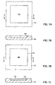
- FIG. 5A is a schematic side view showing the structure of an exemplary embodiment 100 of a band-pass filter in accordance with the invention.
- Figure 5B is a cross-sectional view along the section line 5B-5B in Figure 5A .
- Band-pass filter 100 is composed of a stacked pair of film bulk acoustic resonators (FBARs) 110 and 120.
- FBAR 120 is stacked atop FBAR 110.
- FBAR 110 is composed of opposed planar electrodes 112 and 114 and a layer 116 of piezoelectric material between the electrodes.
- FBAR 120 is composed of opposed planar electrodes 122 and 124 and a layer 126 of piezoelectric material between the electrodes.
- Band-pass filter 100 is also composed of an acoustic decoupler 130 between FBARs 110 and 120, specifically, between electrodes 114 and 122.
- the acoustic decoupler controls the coupling of acoustic energy between FBARs 110 and 120. Specifically, the acoustic decoupler couples less acoustic energy between the FBARs than would be coupled by direct contact between the FBARs as in the exemplary SBAR shown in Figure 3 .
- the stacked FBARs 110 and 120 are suspended over a cavity 104 defined in a substrate 102.
- This way of suspending the stacked FBARs allows the stacked FBARs to resonate mechanically in response to an input electrical signal applied between the electrodes of one of them.
- Other suspension schemes that allow the stacked FBARs to resonate mechanically in response to an input electrical signal are possible.
- the stacked FBARs can be located over a mismatched acoustic Bragg reflector (not shown) formed in or on substrate 102, as disclosed by Lakin in United States patent no. 6,107,721 , the disclosure of which is incorporated into this disclosure by reference.
- acoustic decoupler 130 controls the acoustic coupling between FBARs 110 and 120.
- the acoustic coupling provided by acoustic decoupler 130 is substantially less than the acoustic coupling between the FBARs in the SBAR embodiment shown in Figure 3 .
- band-pass filter 100 has a relatively broad and flat in-band response and a sharp roll-off outside the pass band instead of the single Lorentzian resonance shown in Figure 4 (curve 46) of the over-coupled conventional SBAR.
- the frequency response of band-pass filter 100 will be described further below with reference to Figure 6 .
- FIG 5C is an enlarged view of a first embodiment of acoustic decoupler 130 in which the acoustic decoupler is composed of a layer 131 of acoustic decoupling material located between the electrodes 114 and 122 of FBARs 110 and 120, respectively ( Figure 5B ).
- Layer 131 of acoustic decoupling material has a nominal thickness that is an odd integral multiple of one quarter of the wavelength in the acoustic decoupling material of an acoustic wave having a frequency equal to the center frequency of band-pass filter 100.
- the acoustic decoupling material has an acoustic impedance less than that of the piezoelectric material that constitutes the FBARs 110, 120.
- the acoustic decoupling material additionally has a high electrical resistivity and a low dielectric permittivity.
- the acoustic decoupling material of acoustic decoupler 130 has an acoustic impedance less that of the piezoelectric material of FBARs 110 and 120.
- the acoustic decoupling material also has an acoustic impedance substantially greater than that of air.
- the acoustic impedance of a material is the ratio of stress to particle velocity in the material and is measured in Rayleighs, abbreviated as rayl .
- the piezoelectric material of layers 116, 216 of the FBARs is typically aluminum nitride (AIN).
- the acoustic impedance of A1N is typically about 35 Mrayl and that of molybdenum, a typical electrode material, is about 63 Mrayl.
- the acoustic impedance of air is about 1 krayl.
- materials with an acoustic impedance in the range from about 2 Mrayl to about 16 Mrayl work well as the acoustic decoupling material of layer 131.
- Figure 6 shows how the calculated frequency response of band-pass filter 100 depends on the acoustic impedance of the acoustic decoupling material of layer 131 that constitutes an embodiment of acoustic decoupler 130.
- the embodiment illustrated has a center frequency of about 1,900 MHz.
- Calculated frequency responses for embodiments in which the acoustic decoupling material has an acoustic impedance of about 4 Mrayl, e.g., polyimide, (curve 140), about 8 Mrayl (curve 142) and about 16 Mrayl (curve 144) are shown. It can be seen that the width of the passband of the band-pass filter increases with increasing acoustic impedance of the acoustic decoupling material. Accordingly, by making an appropriate choice of the acoustic decoupling material, embodiments of band-pass filter 100 having a desired pass-band characteristic can be made.
- the embodiment in which the acoustic decoupling material of layer 131 is polyimide exhibits some under coupling of acoustic energy between FBARs 110, 120, but nevertheless has a pass band that is usefully wide.
- the embodiment in which the acoustic decoupling material has an acoustic impedance of about 8 Mrayl exhibits near critical coupling of acoustic energy between FBARs 110, 120.
- the embodiment in which the acoustic impedance of the acoustic decoupling material is about 16 Mrayl (curve 144) exhibits a double peak in the in-band response typical of significant over coupling of acoustic energy between FBARs 110, 120.
- FIG. 6 shows that embodiments in which the acoustic decoupling material has an acoustic impedance of 8 Mrayl or less have an insertion loss of less than 3 dB, and some embodiments have an insertion loss of less than 1 dB.
- the embodiment of acoustic decoupler 130 shown in Figure 5C is composed of layer 131 of acoustic decoupling material with a nominal thickness equal to one quarter of the wavelength in the acoustic decoupling material of an acoustic wave having a frequency equal to the center frequency of the band-pass filter, i.e., t ⁇ ⁇ n /4, where t is the thickness of layer 131 and ⁇ n is the wavelength in the acoustic decoupling material of an acoustic wave having a frequency equal to the center frequency of band-pass filter 100.
- a thickness of layer 131 within approximately ⁇ 10% of the nominal thickness can alternatively be used.
- a thickness outside this range can alternatively be used with some degradation in performance.
- the thickness of layer 131 should differ significantly from 0 ⁇ n at one extreme (see Figure 3 ) and ⁇ n /2 at the other extreme.
- acoustic decoupler 130 shown in Figure 5C is composed of layer 131 of acoustic decoupling material with a nominal thickness equal to an odd integral multiple of one quarter of the wavelength in the acoustic decoupling material of an acoustic wave having a frequency equal to the center frequency of band-pass filter 100, i.e., t ⁇ (2 m + 1) ⁇ n /4, where t and ⁇ n are as defined above and m is an integer equal to or greater than zero.
- a thickness of layer 131 that differs from the nominal thickness by approximately ⁇ 10% of ⁇ n /4 can alternatively be used. A thickness tolerance outside this range can be used with some degradation in performance, but the thickness of layer 131 should differ significantly from an integral multiple of ⁇ n /2.
- layer 131 is formed by spin coating the acoustic decoupling material over electrode 114.
- a layer formed by spin coating will typically have regions of different thickness due to the contouring of the surface coated by the acoustic decoupling material of layer 131.
- the thickness of layer 131 of acoustic decoupling material is the thickness of the portion of the layer located between electrodes 114 and 122.
- plastic materials have acoustic impedances in the range stated above and can be applied in layers of uniform thickness in the thickness ranges stated above. Such plastic materials are therefore potentially suitable for use as the acoustic decoupling material of layer 131 of acoustic decoupler 130.
- the acoustic decoupling material must also be capable of withstanding the temperatures of the fabrication operations performed after layer 131 of acoustic decoupling material has been deposited on electrode 114 to form acoustic decoupler 130.
- electrodes 122 and 124 and piezoelectric layer 126 are deposited by sputtering after layer 131 has been deposited. Temperatures as high as 300°C are reached during these deposition processes. Thus; a plastic that remains stable at such temperatures is used as the acoustic decoupling material.
- Plastic materials typically have a very high acoustic attenuation per unit length compared with the other materials of FBARs 110 and 120.
- acoustic decoupler 130 is composed of layer 131 of plastic acoustic decoupling material typically less than 1 ⁇ m thick, the acoustic attenuation introduced by layer 131 of acoustic decoupling material is typically negligible.
- a polyimide is used as the acoustic decoupling material of layer 131.
- Polyimide is sold under the trademark Kapton® by E.I. du Pont de Nemours and Company.
- acoustic decoupler 130 is composed of layer 131 of polyimide applied to electrode 114 by spin coating.
- Polyimide has an acoustic impedance of about 4 Mrayl.
- a poly(para-xylylene) is used as the acoustic decoupling material of layer 131.
- acoustic decoupler 130 is composed of layer 131 of poly(para-xylylene) applied to electrode 114 by vacuum deposition.
- Poly(para-xylylene) is also known in the art as parylene.
- the dimer precursor di-para-xylylene from which parylene is made and equipment for performing vacuum deposition of layers of parylene are available from many suppliers.
- Parylene has an acoustic impedance of about 2.8 Mrayl.
- the acoustic decoupling material of layer 131 constituting acoustic decoupler 130 has an acoustic impedance substantially greater than the materials of FBARs 110 and 120. No materials having this property are known at this time, but such materials may become available in future, or lower acoustic impedance FBAR materials may become available in future.
- the thickness of layer 131 of such high acoustic impedance acoustic decoupling material is as described above.
- FIG. 5D is an enlarged view of part of band-pass filter 100 showing a second embodiment of acoustic decoupler 130 that incorporates a Bragg structure 161.
- Bragg structure 161 is composed of a low acoustic impedance Bragg element 163 sandwiched between high acoustic impedance Bragg elements 165 and 167.
- Low acoustic impedance Bragg element 163 is a layer of a low acoustic impedance material whereas high acoustic impedance Bragg elements 165 and 167 are each a layer of high acoustic impedance material.
- the acoustic impedances of the materials of the Bragg elements are characterized as "low” and “high” with respect to one another and with respect to the acoustic impedance of the piezoelectric material of layers 116 and 126.
- at least one of the Bragg elements additionally has a high electrical resistivity and a low dielectric permittivity.
- Each of the layers constituting Bragg elements 161, 163 and 165 has a nominal thickness equal to an odd integral multiple of one quarter of the wavelength in the material the layer of an acoustic wave having a frequency equal to the center frequency of band-pass filter 100. Layers that differ from the nominal thickness by approximately 10% of one quarter of the wavelength can alternatively be used. A thickness tolerance outside this range can be used with some degradation in performance, but the thickness of the layers should differ significantly from an integral multiple of one-half of the wavelength.
- low acoustic impedance Bragg element 163 is a layer of silicon dioxide (SiO 2 ), which has an acoustic impedance of about 13 Mrayl
- each of the high acoustic impedance Bragg elements 165 and 167 is a layer of the same material as electrodes 114 and 122, respectively, i.e., molybdenum, which has an acoustic impedance of about 63 Mrayl.
- high acoustic impedance Bragg elements 165 and 167 have a thickness of one quarter of the wavelength in molybdenum of an acoustic wave having a frequency equal to the center frequency of band-pass filter 100
- low acoustic impedance Bragg element 163 has a thickness of three quarters of the wavelength in SiO 2 of an acoustic wave having a frequency equal to the center frequency of the band-pass filter.
- Bragg structure 161 may be composed of more than one (e.g., n ) low acoustic impedance Bragg element interleaved with a corresponding number (i.e., n + 1) of high acoustic impedance Bragg elements. Only one of the Bragg elements need be insulating.
- the Bragg structure may be composed of two low acoustic impedance Bragg elements interleaved with three high acoustic impedance Bragg elements.
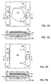
- Wafer-scale fabrication is used to fabricate thousands of band-pass filters similar to band-pass filter 100 at the same time. Such wafer-scale fabrication makes the band-pass filters inexpensive to fabricate.
- An exemplary fabrication method will be described next with reference to the plan views of Figures 7A-7J and the cross-sectional views of Figures 7K-7T .
- a wafer of single-crystal silicon is provided.
- a portion of the wafer constitutes, for each band-pass filter being fabricated, a substrate corresponding to the substrate 102 of band-pass filter 100.
- Figures 7A-7J and Figures 7K-7T illustrate and the following description describes the fabrication of band-pass filter 100 in and on a portion of the wafer. As band-pass filter 100 is fabricated, the remaining band-pass filters on the wafer as similarly fabricated.
- the portion of the wafer that constitutes substrate 102 of band-pass filter 100 is selectively wet etched to form cavity 104, as shown in Figures 7A and 7K .
- a layer of fill material (not shown) is deposited on the surface of the wafer with a thickness sufficient to fill the cavities.
- the surface of the wafer is then planarized to leave the cavities filled with the fill material.
- Figures 7B and 7L show cavity 104 in substrate 102 filled with fill material 105.
- the fill material was phosphosilicate glass (PSG) and was deposited using conventional low-pressure chemical vapor deposition (LPCVD).
- the fill material may alternatively be deposited by sputtering, or by spin coating.
- Electrode 112 typically has an irregular shape in a plane parallel to the major surface of the wafer. An irregular shape minimizes lateral modes in the FBAR 110 of which it forms part, as described in United States patent no. 6,215,375 of Larson III et al ., the disclosure of which is incorporated into this disclosure by reference. Electrode 112 is shaped and located to expose part of the surface of fill material 105 so that the fill material can later be removed by etching, as will be described below.
- electrodes 112, 114, 122 and 124 ( Figure 5B ) are defined are patterned such that, in respective planes parallel to the major surface of the wafer, electrodes 112 and 114 have the same shape, size, orientation and position, electrodes 122 and 124 have the same shape, size, orientation and position, and electrodes 114 and 122 typically have the same shape, size, orientation and position.
- the metal deposited to form electrode 112, bonding pad 132 and trace 133 was molybdenum.
- the molybdenum was deposited with a thickness of about 440 nm by sputtering, and was patterned by dry etching to define a pentagonal electrode with an area of about 26,000 square ⁇ m.
- Other refractory metals such as tungsten, niobium and titanium may alternatively be used as the material of electrode 112, bonding pad 132 and trace 133.
- the electrode, bonding pad and trace may alternatively comprise layers of more than one material.
- a layer of piezoelectric material is deposited and is patterned to define piezoelectric layer 116 as shown in Figures 7D and 7N .
- Piezoelectric layer 116 is patterned to expose part of the surface of fill material 105 and bonding pad 132 of electrode 112.
- Piezoelectric layer 116 is additionally patterned to define windows 119 that provide access to additional parts of the surface of the fill material.
- the piezoelectric material deposited to form piezoelectric layer 116 was aluminum nitride and was deposited with a thickness of about 780 nm by sputtering.
- the piezoelectric material was patterned by wet etching in potassium hydroxide or by chlorine-based dry etching.
- Alternative materials for piezoelectric layer 116 include zinc oxide and lead zirconium titanate.
- a layer of metal is deposited and is patterned to define electrode 114, a bonding pad 134 and an electrical trace 135 extending between electrode 114 and bonding pad 134, as shown in Figures 7E and 7O .
- the metal deposited to form electrode 114 was molybdenum.
- the molybdenum was deposited with a thickness of about 440 nm by sputtering, and was patterned by dry etching.
- Other refractory metals may alternatively be used as the material of electrode 114, bonding pad 134 and trace 135.
- the electrode, bonding pad and trace may alternatively comprise layers of more than one material.
- a layer of acoustic decoupling material is then deposited and is patterned to define acoustic decoupler 130, as shown in Figures 7F and 7P .
- Acoustic decoupler 130 is shaped to cover at least electrode 114, and is additionally shaped to expose part of the surface of fill material 105 and bonding pads 132 and 134. Acoustic decoupler 130 is additionally patterned to define windows 119 that provide access to additional parts of the surface of the fill material.
- the acoustic decoupling material was polyimide with a thickness of about 750 nm, i.e., three quarters of the center frequency wavelength in the polyimide.
- the polyimide was deposited by spin coating, and was patterned by photolithography. Polyimide is photosensitive so that no photoresist is needed.
- other plastic materials can be used as the acoustic decoupling material.
- the acoustic decoupling material can be deposited by methods other than spin coating.
- the wafer was baked at about 300 °C before further processing was performed.
- the bake evaporates volatile constituents of the polyimide and prevents the evaporation of such volatile constituents during subsequent processing from causing subsequently-deposited layers to separate.
- a layer of metal is deposited and is patterned to define electrode 122 and an electrical trace 137 extending from electrode 122 to bonding pad 134, as shown in Figures 7G and 7Q .
- Bonding pad 134 is also electrically connected to electrode 114 by trace 135.
- the metal deposited to form electrode 122 was molybdenum.
- the molybdenum was deposited with a thickness of about 440 nm by sputtering, and was patterned by dry etching.
- Other refractory metals may alternatively be used as the material of electrode 122 and trace 137.
- the electrode and the trace may alternatively comprise layers of more than one material.
- a layer of piezoelectric material is deposited and is patterned to define piezoelectric layer 126.
- Piezoelectric layer 126 is shaped to expose bonding pads 132 and 134 and to expose part of the surface of fill material 105 as shown in Figures 7H and 7R .
- Piezoelectric layer 126 is additionally patterned to define windows 119 that provide access to additional parts of the surface of the fill material.
- the piezoelectric material deposited to form piezoelectric layer 126 was aluminum nitride and was deposited with a thickness of about 780 nm by sputtering.
- the piezoelectric material was patterned by wet etching in potassium hydroxide or by chlorine-based dry etching.
- Alternative materials for piezoelectric layer 126 include zinc oxide and lead zirconium titanate.
- a layer of metal is deposited and is patterned to define electrode 124, a bonding pad 138 and an electrical trace 139 extending from electrode 124 to bonding pad 138, as shown in Figures 7I and 7S .
- the metal deposited to form electrode 124 was molybdenum.
- the molybdenum was deposited with a thickness of about 440 nm by sputtering, and was patterned by dry etching.
- Other refractory metals such may alternatively be used as the material of electrode 124, bonding pad 138 and trace 139.
- the electrode, bonding pad and trace may alternatively comprise layers of more than one material.
- the wafer is then isotropically wet etched to remove fill material 105 from cavity 104. As noted above, portions of the surface of fill material 105 remain exposed through, for example, windows 119. The etch process leaves band-pass filter 100 suspended over cavity 104, as shown in Figures 7J and 7T .
- the etchant used to remove fill material 105 was dilute hydrofluoric acid.
- a gold protective layer is deposited on the exposed surfaces of bonding pads 132, 134 and 138.
- band-pass filter 100 The wafer is then divided into individual band-pass filters, including band-pass filter 100.
- Each band-pass filter is mounted in a package and electrical connections are made between bonding pads 132, 134 and 138 of the band-pass filter and pads that are part of the package.
- acoustic decoupler 130 incorporates a Bragg structure, as shown in Figure 5D , is made by a process similar to that described above. The process differs as follows:
- a layer of metal is deposited and is patterned to define high acoustic impedance Bragg element 165 shown in Figure 5D , bonding pad 134 and electrical trace 135 extending between high acoustic impedance Bragg element 165 and bonding pad 134, in a manner similar to that shown in Figures 7E and 7O .
- the layer of metal is deposited with a nominal thickness equal to an odd, integral multiple of one quarter of the wavelength in the metal of an acoustic wave having a frequency equal to the center frequency of band-pass filter 100.
- High acoustic impedance Bragg element 165 additionally serves as electrode 114 as shown in Figure 5D
- the metal deposited to form high acoustic impedance Bragg element 165 is molybdenum.
- the molybdenum is deposited with a thickness of about 820 nm (one-quarter wavelength in Mo) by sputtering, and is patterned by dry etching.
- Other refractory metals may alternatively be used as the material of high acoustic impedance Bragg element 165, bonding pad 134 and trace 135.
- the high acoustic impedance Bragg element, bonding pad and trace may alternatively comprise layers of more than one metal.
- a layer of low acoustic impedance material is then deposited and is patterned to define low acoustic impedance Bragg element 163 in a manner similar to that shown in Figures 7F and 7P .
- the layer of low acoustic impedance material is deposited with a nominal thickness equal to an odd, integral multiple of one quarter of the wavelength in the material of an acoustic wave having a frequency equal to the center frequency of band-pass filter 100.
- Low acoustic impedance Bragg element 163 is shaped to cover at least high acoustic impedance Bragg element 165, and is additionally shaped to expose part of the surface of fill material 105 and bonding pads 132 and 134.
- the layer of low acoustic impedance material is additionally patterned to define windows 119 that provide access to additional parts of the surface of the fill material.
- the low acoustic impedance material is SiO 2 with a thickness of about 790 nm.
- the SiO 2 is deposited by sputtering, and is patterned by etching.
- Other low acoustic impedance material that can be used as the material of low acoustic impedance Bragg element include phosphosilicate glass (PSG), titanium dioxide and magnesium fluoride.
- PSG phosphosilicate glass
- titanium dioxide titanium dioxide
- magnesium fluoride magnesium fluoride
- a layer of metal is deposited and is patterned to define high acoustic impedance Bragg element 167 shown in Figure 5D and electrical trace 137 extending from high acoustic impedance Bragg element 167 to bonding pad 134 in a manner similar to that shown in Figures 7G and 7Q .
- Bonding pad 134 is also electrically connected to high acoustic impedance Bragg element 167 by trace 135.
- the layer of metal is deposited with a nominal thickness equal to an odd, integral multiple of one quarter of the wavelength in the metal of an acoustic wave having a frequency equal to the center frequency of band-pass filter 100.
- High acoustic impedance Bragg element 167 additionally serves as electrode 122 as shown in Figure 5D .
- the metal deposited to form high acoustic impedance Bragg element 167 and electrical trace 137 is molybdenum.
- the molybdenum is deposited with a thickness of about 820 nm (one-quarter wavelength in Mo) by sputtering, and is patterned by dry etching.
- Other refractory metals may alternatively be used as the material of high acoustic impedance Bragg element 167 and trace 137.
- the high acoustic impedance Bragg element and the trace may alternatively comprise layers of more than one material.
- a layer of piezoelectric material is then deposited and is patterned to define piezoelectric layer 126, as described above with reference to Figures 7H and 7R , and the process continues as described above to complete fabrication of band-pass filter 100.
- Band-pass filter 100 is used as follows. Bonding pad 134 electrically connected to electrodes 114 and 122 provides a ground terminal of the band-pass filter 100, bonding pad 132 electrically connected to electrode 112 provides an input terminal of the band-pass filter 100, and bonding pad 13 8 electrically connected to electrode 124 provides an output terminal of the band-pass filter 100.
- the input terminal and the output terminal can be interchanged.
- band-pass filter 100 may additionally provide electrical isolation between input and output.
- an additional bonding pad (not shown) is defined in the metal in which electrode 122 and trace 137 are defined, and trace 137 extends from electrode 122 to the additional boding pad instead of to bonding pad 134.
- Bonding pad 132 and 134 electrically connected to electrodes 112 and 114, respectively, provide a pair of input terminals and the additional bonding pad (not shown) electrically connected by trace 137 to electrode 122 and bonding pad 138 electrically connected to electrode 124 provide a pair of output terminals.
- the input terminals and the output terminals are electrically isolated from one another. Again, the input terminals and output terminals may be interchanged.
- FIG. 8 is a schematic drawing of an exemplary embodiment 200 of a band-pass filter in accordance with the invention having an out-of-band frequency response that has a steeper slope than that of band-pass filter 100, and in which, after the initial sharp fall, the frequency response rises to a substantially lower level than the band-pass ladder filter shown in Figure 1 .
- Band-pass filter 200 is composed of a simplified FBAR-based ladder filter 210 connected in series with band-pass filter 100 described above with reference to Figures 5A and 5B .
- Ladder filter 210 is composed of series FBARs 212 and 214 and a shunt FBAR 216.
- Series FBARs 212 and 214 have a higher resonant frequency than shunt FBAR 214.
- band-pass filter 100 In band-pass filter 100, electrode 112 is connected to ground, electrodes 114 and 122 are connected to the output of ladder filter 210, i.e., to the electrode 218 of FBAR 214, and electrode 124 provides the output terminal of band-pass filter 200.
- FBARs 212, 214 and 216 and band-pass filter 100 are structured so that band-pass filter 100 has a broader pass band than ladder filter 210.
- Figure 9 is a graph showing the calculated frequency response of band-pass filter 200 (curve 242) and that of band-pass filter 100 shown in Figures 5A and 5B (curve 244).
- the graph shows that the out-of-band frequency response of band-pass filter 200 has a steeper slope than that of band-pass filter 100, and the level to which the frequency response rises after the initial sharp fall is lower than that of the band-pass ladder filter shown in Figure 4 .
- the FBARs constituting an FBAR-based ladder filter are typically all fabricated using a common layer of piezoelectric material.
- Band-pass filter 200 can be fabricated in a similar way.
- FBAR 110 ( Figure 5B ) of band-pass filter 100 is fabricated using the same layer of piezoelectric material as FBARs 212, 214 and 216.
- Electrode 112 of FBAR 110 is part of the same metal layer as the electrode 220 of FBAR 216.
- Electrode 114 of FBAR 110 is part of the same metal layer as the electrode 218 of FBAR 214.
- a layer of acoustic decoupling material is deposited and is patterned to define acoustic decoupler 130 on electrode 114.
- FBAR 120 is then fabricated on the acoustic decoupler using a process similar to that described above.
- Electrodes 222 of FBAR 212 and to the electrode 220 of FBAR 216 provide the input terminals of band-pass filter 200 while electrical connections to electrodes 112 and 124 of band-pass filter 100 provide the output terminals of band-pass filter 200
Claims (11)
- Filtre passe-bande (100), comprenant :une paire empilée de résonateurs acoustiques à couche mince (FBAR) (110, 120), chacun des FBAR comprenant des électrodes planes opposées (par ex., 112, 114) et une couche (116) de matériau piézoélectrique entre les électrodes ; etun découpleur acoustique (130) entre les FBAR qui est conçu pour coupler moins d'énergie acoustique entre les FBAR qu'il n'en serait couplé par contact direct entre les FBAR, dans lequel le découpleur acoustique comprend une couche (131) de matériau de découplage acoustique, dans lequel le matériau de découplage acoustique comprend du plastique ayant une impédance acoustique comprise entre 4 Mrayl et 8 Mrayl.
- Filtre passe-bande selon la revendication 1, dans lequel :le matériau piézoélectrique a une impédance acoustique ; etle matériau de découplage acoustique a une impédance acoustique comprise entre l'impédance acoustique du matériau piézoélectrique et l'impédance acoustique de l'air.
- Filtre passe-bande selon la revendication 1 ou la revendication 2, dans lequel :le filtre passe-bande est caractérisé par une fréquence médiane ; etla couche de matériau de découplage acoustique a une épaisseur nominale égale à un entier impair multiple d'un quart de la longueur d'onde dans le matériau de découplage acoustique d'une onde acoustique ayant une fréquence égale à la fréquence médiane.
- Filtre passe-bande selon l'une des revendications précédentes, dans lequel le matériau plastique comprend du polyimide ou du poly(para-xylylène).
- Filtre passe-bande selon l'une quelconque des revendications précédentes, comprenant de plus une connexion électrique (134, 137) entre des électrodes adjacentes des électrodes des FBAR.
- Filtre passe-bande selon l'une quelconque des revendications précédentes, comprenant de plus un filtre (210) en échelle connecté électriquement en série avec la paire empilée de FBAR.
- Filtre passe-bande selon la revendication 6, dans lequel le filtre en échelle comprend des FBAR supplémentaires (par ex., 212).
- Procédé de filtrage électrique, comprenant :la fourniture d'un filtre passe-bande selon l'une quelconque des revendications précédentes ;l'application d'un signal électrique d'entrée à l'un des FBAR ; etla prise d'un signal électrique de sortie filtré depuis l'autre des FBAR.
- Procédé de fabrication d'un dispositif couplé acoustiquement, le procédé comprenant :la fabrication d'un premier dispositif résonateur acoustique à couche mince (FBAR) (110) ;la fabrication d'un découpleur acoustique sur le premier FBAR (130) ;la fabrication d'un deuxième FBAR (120) sur le découpleur acoustique, comprenant la soumission du découpleur acoustique à une température maximale ; etavant la fabrication du deuxième FBAR, la cuisson du premier FBAR et du découpleur acoustique à une température non inférieure à la température maximale ;dans lequel le découpleur acoustique est conçu pour coupler moins d'énergie acoustique entre les FBAR qu'il n'en serait couplé par contact direct entre les FBAR et comprend une couche (131) de matériau plastique ayant une impédance acoustique comprise entre 4 Mrayl et 8 Mrayl.
- Procédé selon la revendication 9, dans lequel le découpleur acoustique comprend une couche de polyimide.
- Procédé selon la revendication 10, dans lequel la fabrication du découpleur acoustique comprend le dépôt de la couche de polyimide par revêtement par centrifugation.
Applications Claiming Priority (2)
| Application Number | Priority Date | Filing Date | Title |
|---|---|---|---|
| US10/699,289 US7019605B2 (en) | 2003-10-30 | 2003-10-30 | Stacked bulk acoustic resonator band-pass filter with controllable pass bandwidth |
| US699289 | 2003-10-30 |
Publications (2)
| Publication Number | Publication Date |
|---|---|
| EP1528674A1 EP1528674A1 (fr) | 2005-05-04 |
| EP1528674B1 true EP1528674B1 (fr) | 2008-03-19 |
Family
ID=34423441
Family Applications (1)
| Application Number | Title | Priority Date | Filing Date |
|---|---|---|---|
| EP04014569A Expired - Fee Related EP1528674B1 (fr) | 2003-10-30 | 2004-06-22 | Filtre à résonateurs à ondes acoustiques de volume empilés avec largeur de bande passante contrôlable |
Country Status (5)
| Country | Link |
|---|---|
| US (2) | US7019605B2 (fr) |
| EP (1) | EP1528674B1 (fr) |
| JP (1) | JP2005137002A (fr) |
| CN (3) | CN1868121B (fr) |
| DE (1) | DE602004012511T2 (fr) |
Cited By (32)
| Publication number | Priority date | Publication date | Assignee | Title |
|---|---|---|---|---|
| US7675390B2 (en) | 2005-10-18 | 2010-03-09 | Avago Technologies Wireless Ip (Singapore) Pte. Ltd. | Acoustic galvanic isolator incorporating single decoupled stacked bulk acoustic resonator |
| US7714684B2 (en) | 2004-10-01 | 2010-05-11 | Avago Technologies Wireless Ip (Singapore) Pte. Ltd. | Acoustic resonator performance enhancement using alternating frame structure |
| US7732977B2 (en) | 2008-04-30 | 2010-06-08 | Avago Technologies Wireless Ip (Singapore) | Transceiver circuit for film bulk acoustic resonator (FBAR) transducers |
| US7737807B2 (en) | 2005-10-18 | 2010-06-15 | Avago Technologies Wireless Ip (Singapore) Pte. Ltd. | Acoustic galvanic isolator incorporating series-connected decoupled stacked bulk acoustic resonators |
| US7746677B2 (en) | 2006-03-09 | 2010-06-29 | Avago Technologies Wireless Ip (Singapore) Pte. Ltd. | AC-DC converter circuit and power supply |
| US7791434B2 (en) | 2004-12-22 | 2010-09-07 | Avago Technologies Wireless Ip (Singapore) Pte. Ltd. | Acoustic resonator performance enhancement using selective metal etch and having a trench in the piezoelectric |
| US7791435B2 (en) | 2007-09-28 | 2010-09-07 | Avago Technologies Wireless Ip (Singapore) Pte. Ltd. | Single stack coupled resonators having differential output |
| US7802349B2 (en) | 2003-03-07 | 2010-09-28 | Avago Technologies Wireless Ip (Singapore) Pte. Ltd. | Manufacturing process for thin film bulk acoustic resonator (FBAR) filters |
| US7852644B2 (en) | 2005-10-31 | 2010-12-14 | Avago Technologies General Ip (Singapore) Pte. Ltd. | AC-DC power converter |
| US7855618B2 (en) | 2008-04-30 | 2010-12-21 | Avago Technologies Wireless Ip (Singapore) Pte. Ltd. | Bulk acoustic resonator electrical impedance transformers |
| US7868522B2 (en) | 2005-09-09 | 2011-01-11 | Avago Technologies Wireless Ip (Singapore) Pte. Ltd. | Adjusted frequency temperature coefficient resonator |
| US8080854B2 (en) | 2006-03-10 | 2011-12-20 | Avago Technologies General Ip (Singapore) Pte. Ltd. | Electronic device on substrate with cavity and mitigated parasitic leakage path |
| US8143082B2 (en) | 2004-12-15 | 2012-03-27 | Avago Technologies Wireless Ip (Singapore) Pte. Ltd. | Wafer bonding of micro-electro mechanical systems to active circuitry |
| US8193877B2 (en) | 2009-11-30 | 2012-06-05 | Avago Technologies Wireless Ip (Singapore) Pte. Ltd. | Duplexer with negative phase shifting circuit |
| US8230562B2 (en) | 2005-04-06 | 2012-07-31 | Avago Technologies Wireless Ip (Singapore) Pte. Ltd. | Method of fabricating an acoustic resonator comprising a filled recessed region |
| US8248185B2 (en) | 2009-06-24 | 2012-08-21 | Avago Technologies Wireless Ip (Singapore) Pte. Ltd. | Acoustic resonator structure comprising a bridge |
| US8350445B1 (en) | 2011-06-16 | 2013-01-08 | Avago Technologies Wireless Ip (Singapore) Pte. Ltd. | Bulk acoustic resonator comprising non-piezoelectric layer and bridge |
| US8575820B2 (en) | 2011-03-29 | 2013-11-05 | Avago Technologies General Ip (Singapore) Pte. Ltd. | Stacked bulk acoustic resonator |
| US8796904B2 (en) | 2011-10-31 | 2014-08-05 | Avago Technologies General Ip (Singapore) Pte. Ltd. | Bulk acoustic resonator comprising piezoelectric layer and inverse piezoelectric layer |
| US8902023B2 (en) | 2009-06-24 | 2014-12-02 | Avago Technologies General Ip (Singapore) Pte. Ltd. | Acoustic resonator structure having an electrode with a cantilevered portion |
| US8922302B2 (en) | 2011-08-24 | 2014-12-30 | Avago Technologies General Ip (Singapore) Pte. Ltd. | Acoustic resonator formed on a pedestal |
| US8962443B2 (en) | 2011-01-31 | 2015-02-24 | Avago Technologies General Ip (Singapore) Pte. Ltd. | Semiconductor device having an airbridge and method of fabricating the same |
| US8981876B2 (en) | 2004-11-15 | 2015-03-17 | Avago Technologies General Ip (Singapore) Pte. Ltd. | Piezoelectric resonator structures and electrical filters having frame elements |
| US9048812B2 (en) | 2011-02-28 | 2015-06-02 | Avago Technologies General Ip (Singapore) Pte. Ltd. | Bulk acoustic wave resonator comprising bridge formed within piezoelectric layer |
| US9083302B2 (en) | 2011-02-28 | 2015-07-14 | Avago Technologies General Ip (Singapore) Pte. Ltd. | Stacked bulk acoustic resonator comprising a bridge and an acoustic reflector along a perimeter of the resonator |
| US9136818B2 (en) | 2011-02-28 | 2015-09-15 | Avago Technologies General Ip (Singapore) Pte. Ltd. | Stacked acoustic resonator comprising a bridge |
| US9148117B2 (en) | 2011-02-28 | 2015-09-29 | Avago Technologies General Ip (Singapore) Pte. Ltd. | Coupled resonator filter comprising a bridge and frame elements |
| US9154112B2 (en) | 2011-02-28 | 2015-10-06 | Avago Technologies General Ip (Singapore) Pte. Ltd. | Coupled resonator filter comprising a bridge |
| US9203374B2 (en) | 2011-02-28 | 2015-12-01 | Avago Technologies General Ip (Singapore) Pte. Ltd. | Film bulk acoustic resonator comprising a bridge |
| US9243316B2 (en) | 2010-01-22 | 2016-01-26 | Avago Technologies General Ip (Singapore) Pte. Ltd. | Method of fabricating piezoelectric material with selected c-axis orientation |
| US9425764B2 (en) | 2012-10-25 | 2016-08-23 | Avago Technologies General Ip (Singapore) Pte. Ltd. | Accoustic resonator having composite electrodes with integrated lateral features |
| US9444426B2 (en) | 2012-10-25 | 2016-09-13 | Avago Technologies General Ip (Singapore) Pte. Ltd. | Accoustic resonator having integrated lateral feature and temperature compensation feature |
Families Citing this family (70)
| Publication number | Priority date | Publication date | Assignee | Title |
|---|---|---|---|---|
| US7019605B2 (en) * | 2003-10-30 | 2006-03-28 | Larson Iii John D | Stacked bulk acoustic resonator band-pass filter with controllable pass bandwidth |
| US7391285B2 (en) * | 2003-10-30 | 2008-06-24 | Avago Technologies Wireless Ip Pte Ltd | Film acoustically-coupled transformer |
| EP1528677B1 (fr) * | 2003-10-30 | 2006-05-10 | Agilent Technologies, Inc. | Transformateur à couplage acoustique de couches minces avec deux éléments piézoélectriques à axe-c inversé |
| US6946928B2 (en) * | 2003-10-30 | 2005-09-20 | Agilent Technologies, Inc. | Thin-film acoustically-coupled transformer |
| US7332985B2 (en) * | 2003-10-30 | 2008-02-19 | Avago Technologies Wireless Ip (Singapore) Pte Ltd. | Cavity-less film bulk acoustic resonator (FBAR) devices |
| KR20050066104A (ko) * | 2003-12-26 | 2005-06-30 | 삼성전기주식회사 | Fbar 소자 및 그 제조방법 |
| DE102004054895B4 (de) * | 2004-11-12 | 2007-04-19 | Infineon Technologies Ag | Dünnschicht-BAW-Filter sowie Verfahren zur Herstellung eines Dünnschicht-BAW-Filters |
| US7427819B2 (en) * | 2005-03-04 | 2008-09-23 | Avago Wireless Ip Pte Ltd | Film-bulk acoustic wave resonator with motion plate and method |
| US7436269B2 (en) * | 2005-04-18 | 2008-10-14 | Avago Technologies Wireless Ip (Singapore) Pte. Ltd. | Acoustically coupled resonators and method of making the same |
| US7934884B2 (en) * | 2005-04-27 | 2011-05-03 | Lockhart Industries, Inc. | Ring binder cover |
| US7562429B2 (en) * | 2005-06-20 | 2009-07-21 | Avago Technologies General Ip (Singapore) Pte. Ltd. | Suspended device and method of making |
| US7443269B2 (en) | 2005-07-27 | 2008-10-28 | Avago Technologies General Ip (Singapore) Pte. Ltd. | Method and apparatus for selectively blocking radio frequency (RF) signals in a radio frequency (RF) switching circuit |
| US7391286B2 (en) * | 2005-10-06 | 2008-06-24 | Avago Wireless Ip Pte Ltd | Impedance matching and parasitic capacitor resonance of FBAR resonators and coupled filters |
| US7423503B2 (en) * | 2005-10-18 | 2008-09-09 | Avago Technologies Wireless Ip (Singapore) Pte. Ltd. | Acoustic galvanic isolator incorporating film acoustically-coupled transformer |
| US7425787B2 (en) * | 2005-10-18 | 2008-09-16 | Avago Technologies Wireless Ip (Singapore) Pte. Ltd. | Acoustic galvanic isolator incorporating single insulated decoupled stacked bulk acoustic resonator with acoustically-resonant electrical insulator |
| US7525398B2 (en) * | 2005-10-18 | 2009-04-28 | Avago Technologies General Ip (Singapore) Pte. Ltd. | Acoustically communicating data signals across an electrical isolation barrier |
| KR100904621B1 (ko) * | 2005-11-04 | 2009-06-25 | 가부시키가이샤 무라타 세이사쿠쇼 | 압전 박막 공진자 |
| US7561009B2 (en) * | 2005-11-30 | 2009-07-14 | Avago Technologies General Ip (Singapore) Pte. Ltd. | Film bulk acoustic resonator (FBAR) devices with temperature compensation |
| US7612636B2 (en) * | 2006-01-30 | 2009-11-03 | Avago Technologies Wireless Ip (Singapore) Pte. Ltd. | Impedance transforming bulk acoustic wave baluns |
| US20070210724A1 (en) * | 2006-03-09 | 2007-09-13 | Mark Unkrich | Power adapter and DC-DC converter having acoustic transformer |
| US20070228876A1 (en) * | 2006-03-31 | 2007-10-04 | Chien-Min Sung | Diamond Frequency Control Devices and Associated Methods |
| US7586389B2 (en) * | 2006-06-19 | 2009-09-08 | Maxim Integrated Products, Inc. | Impedance transformation and filter using bulk acoustic wave technology |
| US7598827B2 (en) * | 2006-06-19 | 2009-10-06 | Maxim Integrated Products | Harmonic termination of power amplifiers using BAW filter output matching circuits |
| US8925163B2 (en) | 2006-09-18 | 2015-01-06 | Teknologian Tutkimuskeskus Vtt | Method of manufacturing laterally coupled BAW thin films |
| FI121722B (fi) * | 2006-09-18 | 2011-03-15 | Valtion Teknillinen | Levykondensaattori- tai levyresonaattorijärjestely |
| US7508286B2 (en) * | 2006-09-28 | 2009-03-24 | Avago Technologies Wireless Ip (Singapore) Pte. Ltd. | HBAR oscillator and method of manufacture |
| JP2008172711A (ja) * | 2007-01-15 | 2008-07-24 | Hitachi Media Electoronics Co Ltd | 薄膜バルク弾性波共振器およびフィルタおよびそれを用いた高周波モジュール |
| JP2008245243A (ja) * | 2007-02-26 | 2008-10-09 | Epson Toyocom Corp | 輪郭振動子、輪郭振動子の調整方法 |
| US20080202239A1 (en) * | 2007-02-28 | 2008-08-28 | Fazzio R Shane | Piezoelectric acceleration sensor |
| US7777318B2 (en) * | 2007-07-24 | 2010-08-17 | Northrop Grumman Systems Corporation | Wafer level packaging integrated hydrogen getter |
| CN101695176A (zh) | 2007-09-06 | 2010-04-14 | 夏普株式会社 | 通信设备和通信方法 |
| US20090079520A1 (en) * | 2007-09-20 | 2009-03-26 | Avago Technologies Wireless Ip (Singapore) Pte. Ltd. | Acoustically coupled resonators having resonant transmission minima |
| US20090079514A1 (en) * | 2007-09-24 | 2009-03-26 | Tiberiu Jamneala | Hybrid acoustic resonator-based filters |
| US7786826B2 (en) * | 2007-10-12 | 2010-08-31 | Avago Technologies Wireless Ip (Singapore) Pte. Ltd. | Apparatus with acoustically coupled BAW resonators and a method for matching impedances |
| JP5279068B2 (ja) * | 2008-02-15 | 2013-09-04 | 太陽誘電株式会社 | 圧電薄膜共振子、フィルタ、通信モジュール、および通信装置 |
| JP5226409B2 (ja) | 2008-07-17 | 2013-07-03 | 太陽誘電株式会社 | 共振デバイス、通信モジュール、通信装置、共振デバイスの製造方法 |
| KR101289982B1 (ko) | 2009-01-09 | 2013-07-26 | 다이요 유덴 가부시키가이샤 | 필터 소자, 분파기 및 전자 장치 |
| US8291559B2 (en) * | 2009-02-24 | 2012-10-23 | Epcos Ag | Process for adapting resonance frequency of a BAW resonator |
| US8198958B1 (en) * | 2009-03-30 | 2012-06-12 | Triquint Semiconductor, Inc. | Power amplifier matching RF system and method using bulk acoustics wave device |
| US9847768B2 (en) * | 2009-11-23 | 2017-12-19 | Avago Technologies General Ip (Singapore) Pte. Ltd. | Polarity determining seed layer and method of fabricating piezoelectric materials with specific C-axis |
| US8283999B2 (en) * | 2010-02-23 | 2012-10-09 | Avago Technologies Wireless Ip (Singapore) Pte. Ltd. | Bulk acoustic resonator structures comprising a single material acoustic coupling layer comprising inhomogeneous acoustic property |
| US8587391B2 (en) * | 2010-02-23 | 2013-11-19 | Avago Technologies General Ip (Singapore) Pte. Ltd. | Acoustic coupling layer for coupled resonator filters and method of fabricating acoustic coupling layer |
| JP5519326B2 (ja) | 2010-02-25 | 2014-06-11 | 太陽誘電株式会社 | フィルタ、デュープレクサ、通信モジュール、通信装置 |
| US8390397B2 (en) * | 2010-03-29 | 2013-03-05 | Avago Technologies Wireless Ip (Singapore) Pte. Ltd. | Bulk acoustic resonator structure comprising hybrid electrodes |
| US20120066876A1 (en) * | 2010-09-16 | 2012-03-22 | Huffman James D | Creating an improved piezoelectric layer for transducers |
| CN101958696B (zh) * | 2010-09-27 | 2013-04-17 | 张�浩 | 温度补偿薄膜体波谐振器及加工方法 |
| JP5643056B2 (ja) | 2010-11-01 | 2014-12-17 | 太陽誘電株式会社 | 弾性波デバイス |
| US9490418B2 (en) | 2011-03-29 | 2016-11-08 | Avago Technologies General Ip (Singapore) Pte. Ltd. | Acoustic resonator comprising collar and acoustic reflector with temperature compensating layer |
| US9490771B2 (en) | 2012-10-29 | 2016-11-08 | Avago Technologies General Ip (Singapore) Pte. Ltd. | Acoustic resonator comprising collar and frame |
| US9401692B2 (en) | 2012-10-29 | 2016-07-26 | Avago Technologies General Ip (Singapore) Pte. Ltd. | Acoustic resonator having collar structure |
| JP5394451B2 (ja) * | 2011-07-26 | 2014-01-22 | 株式会社アドバンテスト | アクチュエータの製造方法、スイッチ装置、伝送路切替装置、および試験装置 |
| US11595760B2 (en) | 2011-12-23 | 2023-02-28 | Shenzhen Shokz Co., Ltd. | Bone conduction speaker and compound vibration device thereof |
| US9608592B2 (en) * | 2014-01-21 | 2017-03-28 | Avago Technologies General Ip (Singapore) Pte. Ltd. | Film bulk acoustic wave resonator (FBAR) having stress-relief |
| US8941286B2 (en) * | 2012-02-14 | 2015-01-27 | Taiyo Yuden Co., Ltd. | Acoustic wave device |
| US9385684B2 (en) | 2012-10-23 | 2016-07-05 | Avago Technologies General Ip (Singapore) Pte. Ltd. | Acoustic resonator having guard ring |
| TWI493868B (zh) | 2013-01-02 | 2015-07-21 | Ind Tech Res Inst | 微機電共振裝置 |
| JP6185292B2 (ja) * | 2013-06-10 | 2017-08-23 | 太陽誘電株式会社 | 弾性波デバイス |
| CN103607178B (zh) * | 2013-09-17 | 2016-10-05 | 诺思(天津)微系统有限公司 | 薄膜体波谐振器及提高其品质因数的方法 |
| CN103701425B (zh) * | 2013-10-25 | 2017-05-03 | 诺思(天津)微系统有限公司 | 滤波器及其制造方法 |
| US11627419B2 (en) | 2014-01-06 | 2023-04-11 | Shenzhen Shokz Co., Ltd. | Systems and methods for suppressing sound leakage |
| DE102014111993B4 (de) * | 2014-08-21 | 2017-12-21 | Snaptrack, Inc. | Mikroakustische Bauelement mit verbesserter Temperaturkompensation |
| CN107340317A (zh) * | 2017-06-19 | 2017-11-10 | 天津大学 | 一种气体识别方法、气体传感器及气体识别装置 |
| CN107453729B (zh) * | 2017-06-28 | 2021-04-06 | 中国电子科技集团公司第五十五研究所 | 一种基于复合结构的温度补偿薄膜体声波谐振器 |
| US10476480B1 (en) | 2018-07-06 | 2019-11-12 | Globalfoundries Singapore Pte. Ltd. | Dual-mode MEMS resonator, oscillator, sensor, timing device, acoustic filter and front-end module and the methods of making |
| WO2020220721A1 (fr) | 2019-04-30 | 2020-11-05 | 深圳市韶音科技有限公司 | Dispositif de sortie acoustique |
| CN110082376B (zh) * | 2019-05-20 | 2024-01-30 | 中国人民大学 | 一种双列单晶中子分析器单元 |
| CN110460307B (zh) * | 2019-07-31 | 2023-07-14 | 华南理工大学 | 一种温度自适应fbar振荡电路 |
| CN111740003A (zh) * | 2020-06-22 | 2020-10-02 | 济南晶正电子科技有限公司 | 一种压电薄膜体及其制备方法、空腔型器件及其制备方法 |
| CN112383286B (zh) * | 2020-08-04 | 2021-09-21 | 诺思(天津)微系统有限责任公司 | 体声波谐振器组件及其制造方法、滤波器及电子设备 |
| CN114070224A (zh) * | 2020-08-06 | 2022-02-18 | 诺思(天津)微系统有限责任公司 | 带声学解耦层的体声波谐振器组件及制造方法、滤波器及电子设备 |
Family Cites Families (149)
| Publication number | Priority date | Publication date | Assignee | Title |
|---|---|---|---|---|
| FR1307476A (fr) * | 1960-12-12 | 1962-10-26 | U S Sonics Corp | Amplificateur sélecteur de fréquences |
| US3189851A (en) * | 1962-06-04 | 1965-06-15 | Sonus Corp | Piezoelectric filter |
| US3321648A (en) * | 1964-06-04 | 1967-05-23 | Sonus Corp | Piezoelectric filter element |
| GB1207974A (en) | 1966-11-17 | 1970-10-07 | Clevite Corp | Frequency selective apparatus including a piezoelectric device |
| US3422371A (en) * | 1967-07-24 | 1969-01-14 | Sanders Associates Inc | Thin film piezoelectric oscillator |
| US3826931A (en) | 1967-10-26 | 1974-07-30 | Hewlett Packard Co | Dual crystal resonator apparatus |
| US3582839A (en) | 1968-06-06 | 1971-06-01 | Clevite Corp | Composite coupled-mode filter |
| US3607761A (en) | 1968-12-09 | 1971-09-21 | Continental Oil Co | Soap bars containing salts of fatty acids derived from the guerbet reaction |
| US3610969A (en) * | 1970-02-06 | 1971-10-05 | Mallory & Co Inc P R | Monolithic piezoelectric resonator for use as filter or transformer |
| US3845402A (en) | 1973-02-15 | 1974-10-29 | Edmac Ass Inc | Sonobuoy receiver system, floating coupler |
| FR2380666A1 (fr) | 1977-02-14 | 1978-09-08 | Cii Honeywell Bull | Systeme de commande de decoupage pour convertisseur dans une alimentation electrique continue |
| US4084217A (en) | 1977-04-19 | 1978-04-11 | Bbc Brown, Boveri & Company, Limited | Alternating-current fed power supply |
| GB2033185B (en) | 1978-09-22 | 1983-05-18 | Secr Defence | Acoustic wave device with temperature stabilisation |
| US4281299A (en) | 1979-11-23 | 1981-07-28 | Honeywell Inc. | Signal isolator |
| ZA81781B (en) | 1980-02-13 | 1982-03-31 | Int Computers Ltd | Digital systems |
| US4320365A (en) | 1980-11-03 | 1982-03-16 | United Technologies Corporation | Fundamental, longitudinal, thickness mode bulk wave resonator |
| JPS58137317A (ja) | 1982-02-09 | 1983-08-15 | Nec Corp | 圧電薄膜複合振動子 |
| GB2137056B (en) | 1983-03-16 | 1986-09-03 | Standard Telephones Cables Ltd | Communications apparatus |
| US4625138A (en) | 1984-10-24 | 1986-11-25 | The United States Of America As Represented By The Secretary Of The Army | Piezoelectric microwave resonator using lateral excitation |
| US4719383A (en) | 1985-05-20 | 1988-01-12 | The United States Of America As Represented By The United States Department Of Energy | Piezoelectric shear wave resonator and method of making same |
| SE465946B (sv) | 1986-09-11 | 1991-11-18 | Bengt Henoch | Anordning foer oeverfoering av elektrisk energi till elektrisk utrustning genom omagnetiska och elektriskt isolerande material |
| US4906840A (en) | 1988-01-27 | 1990-03-06 | The Board Of Trustees Of Leland Stanford Jr., University | Integrated scanning tunneling microscope |
| US4841429A (en) | 1988-03-24 | 1989-06-20 | Hughes Aircraft Company | Capacitive coupled power supplies |
| US4836882A (en) | 1988-09-12 | 1989-06-06 | The United States Of America As Represented By The Secretary Of The Army | Method of making an acceleration hardened resonator |
| US5118982A (en) | 1989-05-31 | 1992-06-02 | Nec Corporation | Thickness mode vibration piezoelectric transformer |
| US5048036A (en) | 1989-09-18 | 1991-09-10 | Spectra Diode Laboratories, Inc. | Heterostructure laser with lattice mismatch |
| DE69129879T2 (de) | 1990-05-22 | 1999-02-18 | Canon Kk | Datenaufzeichnungsgerät |
| US5241456A (en) | 1990-07-02 | 1993-08-31 | General Electric Company | Compact high density interconnect structure |
| JP2995076B2 (ja) | 1990-07-24 | 1999-12-27 | 富士通株式会社 | 半導体装置 |
| US5162691A (en) | 1991-01-22 | 1992-11-10 | The United States Of America As Represented By The Secretary Of The Army | Cantilevered air-gap type thin film piezoelectric resonator |
| US5294898A (en) * | 1992-01-29 | 1994-03-15 | Motorola, Inc. | Wide bandwidth bandpass filter comprising parallel connected piezoelectric resonators |
| US5382930A (en) | 1992-12-21 | 1995-01-17 | Trw Inc. | Monolithic multipole filters made of thin film stacked crystal filters |
| US5384808A (en) | 1992-12-31 | 1995-01-24 | Apple Computer, Inc. | Method and apparatus for transmitting NRZ data signals across an isolation barrier disposed in an interface between adjacent devices on a bus |
| US5448014A (en) | 1993-01-27 | 1995-09-05 | Trw Inc. | Mass simultaneous sealing and electrical connection of electronic devices |
| US5465725A (en) | 1993-06-15 | 1995-11-14 | Hewlett Packard Company | Ultrasonic probe |
| US5587620A (en) | 1993-12-21 | 1996-12-24 | Hewlett-Packard Company | Tunable thin film acoustic resonators and method for making the same |
| US5594705A (en) | 1994-02-04 | 1997-01-14 | Dynamotive Canada Corporation | Acoustic transformer with non-piezoelectric core |
| US5864261A (en) * | 1994-05-23 | 1999-01-26 | Iowa State University Research Foundation | Multiple layer acoustical structures for thin-film resonator based circuits and systems |
| JPH0878786A (ja) | 1994-09-02 | 1996-03-22 | Mitsubishi Electric Corp | 歪量子井戸の構造 |
| US5692279A (en) | 1995-08-17 | 1997-12-02 | Motorola | Method of making a monolithic thin film resonator lattice filter |
| CN1183587C (zh) | 1996-04-08 | 2005-01-05 | 德克萨斯仪器股份有限公司 | 用于把两个集成电路直流上相互隔离的方法和设备 |
| US5714917A (en) | 1996-10-02 | 1998-02-03 | Nokia Mobile Phones Limited | Device incorporating a tunable thin film bulk acoustic resonator for performing amplitude and phase modulation |
| US5873154A (en) * | 1996-10-17 | 1999-02-23 | Nokia Mobile Phones Limited | Method for fabricating a resonator having an acoustic mirror |
| US6087198A (en) | 1998-02-12 | 2000-07-11 | Texas Instruments Incorporated | Low cost packaging for thin-film resonators and thin-film resonator-based filters |
| US5872493A (en) | 1997-03-13 | 1999-02-16 | Nokia Mobile Phones, Ltd. | Bulk acoustic wave (BAW) filter having a top portion that includes a protective acoustic mirror |
| US5853601A (en) | 1997-04-03 | 1998-12-29 | Northrop Grumman Corporation | Top-via etch technique for forming dielectric membranes |
| US6339048B1 (en) * | 1999-12-23 | 2002-01-15 | Elementis Specialties, Inc. | Oil and oil invert emulsion drilling fluids with improved anti-settling properties |
| US6040962A (en) | 1997-05-14 | 2000-03-21 | Tdk Corporation | Magnetoresistive element with conductive films and magnetic domain films overlapping a central active area |
| US5910756A (en) * | 1997-05-21 | 1999-06-08 | Nokia Mobile Phones Limited | Filters and duplexers utilizing thin film stacked crystal filter structures and thin film bulk acoustic wave resonators |
| JP3378775B2 (ja) | 1997-07-07 | 2003-02-17 | 株式会社村田製作所 | 圧電共振子およびその周波数調整方法 |
| US5982297A (en) | 1997-10-08 | 1999-11-09 | The Aerospace Corporation | Ultrasonic data communication system |
| US6873065B2 (en) * | 1997-10-23 | 2005-03-29 | Analog Devices, Inc. | Non-optical signal isolator |
| US6197261B1 (en) * | 1998-02-02 | 2001-03-06 | Richard A. Linville | Machine for opening blood segments |
| US5936150A (en) | 1998-04-13 | 1999-08-10 | Rockwell Science Center, Llc | Thin film resonant chemical sensor with resonant acoustic isolator |
| US5953479A (en) | 1998-05-07 | 1999-09-14 | The United States Of America As Represented By The Secretary Of The Army | Tilted valance-band quantum well double heterostructures for single step active and passive optical waveguide device monolithic integration |
| KR100328807B1 (ko) | 1998-05-08 | 2002-03-14 | 가네코 히사시 | 제조비용이 저렴하고 충분한 접착 강도가 수득될 수 있는 수지구조물 및 이의 제조 방법 |
| JPH11345406A (ja) | 1998-05-29 | 1999-12-14 | Sony Corp | マスクパターンの形成方法及び薄膜磁気ヘッドの製造方法 |
| US6060818A (en) | 1998-06-02 | 2000-05-09 | Hewlett-Packard Company | SBAR structures and method of fabrication of SBAR.FBAR film processing techniques for the manufacturing of SBAR/BAR filters |
| DE19826152A1 (de) | 1998-06-12 | 1999-12-16 | Thomson Brandt Gmbh | Anordnung mit einem Schaltnetzteil und einem Mikroprozessor |
| US6150703A (en) | 1998-06-29 | 2000-11-21 | Trw Inc. | Lateral mode suppression in semiconductor bulk acoustic resonator (SBAR) devices using tapered electrodes, and electrodes edge damping materials |
| US6252229B1 (en) | 1998-07-10 | 2001-06-26 | Boeing North American, Inc. | Sealed-cavity microstructure and microbolometer and associated fabrication methods |
| WO2000028606A1 (fr) | 1998-11-09 | 2000-05-18 | Richard Patten Bishop | Dispositif piezo-electrique multicouche de transfert d'energie electrique |
| JP3414381B2 (ja) | 1998-12-22 | 2003-06-09 | セイコーエプソン株式会社 | 電力給電装置、電力受電装置、電力伝送システム、電力伝送方法、携帯機器および時計装置 |
| FI113211B (fi) * | 1998-12-30 | 2004-03-15 | Nokia Corp | Balansoitu suodatinrakenne ja matkaviestinlaite |
| JP3438690B2 (ja) * | 1999-01-22 | 2003-08-18 | 株式会社村田製作所 | 弾性表面波装置の周波数調整方法 |
| US6215375B1 (en) | 1999-03-30 | 2001-04-10 | Agilent Technologies, Inc. | Bulk acoustic wave resonator with improved lateral mode suppression |
| JP3531522B2 (ja) | 1999-04-19 | 2004-05-31 | 株式会社村田製作所 | 圧電共振子 |
| US6262637B1 (en) | 1999-06-02 | 2001-07-17 | Agilent Technologies, Inc. | Duplexer incorporating thin-film bulk acoustic resonators (FBARs) |
| DE19931297A1 (de) * | 1999-07-07 | 2001-01-11 | Philips Corp Intellectual Pty | Volumenwellen-Filter |
| US6265246B1 (en) | 1999-07-23 | 2001-07-24 | Agilent Technologies, Inc. | Microcap wafer-level package |
| JP4420538B2 (ja) | 1999-07-23 | 2010-02-24 | アバゴ・テクノロジーズ・ワイヤレス・アイピー(シンガポール)プライベート・リミテッド | ウェーハパッケージの製造方法 |
| US6228675B1 (en) | 1999-07-23 | 2001-05-08 | Agilent Technologies, Inc. | Microcap wafer-level package with vias |
| US6107721A (en) | 1999-07-27 | 2000-08-22 | Tfr Technologies, Inc. | Piezoelectric resonators on a differentially offset reflector |
| US6292336B1 (en) | 1999-09-30 | 2001-09-18 | Headway Technologies, Inc. | Giant magnetoresistive (GMR) sensor element with enhanced magnetoresistive (MR) coefficient |
| JP2001196883A (ja) | 1999-11-01 | 2001-07-19 | Murata Mfg Co Ltd | 圧電共振素子の周波数調整方法 |
| US6307447B1 (en) | 1999-11-01 | 2001-10-23 | Agere Systems Guardian Corp. | Tuning mechanical resonators for electrical filter |
| US6441539B1 (en) | 1999-11-11 | 2002-08-27 | Murata Manufacturing Co., Ltd. | Piezoelectric resonator |
| JP2001244778A (ja) * | 1999-12-22 | 2001-09-07 | Toyo Commun Equip Co Ltd | 高周波圧電振動子 |
| EP1117017B1 (fr) * | 2000-01-10 | 2009-09-09 | ETA SA Manufacture Horlogère Suisse | Dispositif pour produire un signal ayant une fréquence sensiblement indépendante de la température |
| US6521477B1 (en) * | 2000-02-02 | 2003-02-18 | Raytheon Company | Vacuum package fabrication of integrated circuit components |
| US6479320B1 (en) | 2000-02-02 | 2002-11-12 | Raytheon Company | Vacuum package fabrication of microelectromechanical system devices with integrated circuit components |
| US6466418B1 (en) | 2000-02-11 | 2002-10-15 | Headway Technologies, Inc. | Bottom spin valves with continuous spacer exchange (or hard) bias |
| US6262600B1 (en) | 2000-02-14 | 2001-07-17 | Analog Devices, Inc. | Isolator for transmitting logic signals across an isolation barrier |
| DE10007577C1 (de) | 2000-02-18 | 2001-09-13 | Infineon Technologies Ag | Piezoresonator |
| US6441481B1 (en) * | 2000-04-10 | 2002-08-27 | Analog Devices, Inc. | Hermetically sealed microstructure package |
| US6384697B1 (en) | 2000-05-08 | 2002-05-07 | Agilent Technologies, Inc. | Cavity spanning bottom electrode of a substrate-mounted bulk wave acoustic resonator |
| GB0012439D0 (en) * | 2000-05-24 | 2000-07-12 | Univ Cranfield | Improvements to filters |
| US6420820B1 (en) | 2000-08-31 | 2002-07-16 | Agilent Technologies, Inc. | Acoustic wave resonator and method of operating the same to maintain resonance when subjected to temperature variations |
| US6377137B1 (en) | 2000-09-11 | 2002-04-23 | Agilent Technologies, Inc. | Acoustic resonator filter with reduced electromagnetic influence due to die substrate thickness |
| US6530515B1 (en) | 2000-09-26 | 2003-03-11 | Amkor Technology, Inc. | Micromachine stacked flip chip package fabrication method |
| US6486751B1 (en) * | 2000-09-26 | 2002-11-26 | Agere Systems Inc. | Increased bandwidth thin film resonator having a columnar structure |
| JP2002120364A (ja) * | 2000-10-17 | 2002-04-23 | Fuji Xerox Co Ltd | 音響波インクジェット記録ヘッド及び音響波インクジェット記録装置 |
| US6542055B1 (en) | 2000-10-31 | 2003-04-01 | Agilent Technologies, Inc. | Integrated filter balun |
| DE60110827T2 (de) | 2000-11-03 | 2006-01-12 | Paratek Microwave, Inc. | Verfahren zur kanalfrequenzzuteilung für hf- und mikrowellenduplexer |
| US6515558B1 (en) * | 2000-11-06 | 2003-02-04 | Nokia Mobile Phones Ltd | Thin-film bulk acoustic resonator with enhanced power handling capacity |
| GB0029090D0 (en) * | 2000-11-29 | 2001-01-10 | Univ Cranfield | Improvements in or relating to filters |
| US6550664B2 (en) | 2000-12-09 | 2003-04-22 | Agilent Technologies, Inc. | Mounting film bulk acoustic resonators in microwave packages using flip chip bonding technology |
| US6424237B1 (en) | 2000-12-21 | 2002-07-23 | Agilent Technologies, Inc. | Bulk acoustic resonator perimeter reflection system |
| US6518860B2 (en) | 2001-01-05 | 2003-02-11 | Nokia Mobile Phones Ltd | BAW filters having different center frequencies on a single substrate and a method for providing same |
| US6407649B1 (en) | 2001-01-05 | 2002-06-18 | Nokia Corporation | Monolithic FBAR duplexer and method of making the same |
| US6512300B2 (en) * | 2001-01-10 | 2003-01-28 | Raytheon Company | Water level interconnection |
| US6462631B2 (en) | 2001-02-14 | 2002-10-08 | Agilent Technologies, Inc. | Passband filter having an asymmetrical filter response |
| US6583374B2 (en) | 2001-02-20 | 2003-06-24 | Rockwell Automation Technologies, Inc. | Microelectromechanical system (MEMS) digital electrical isolator |
| US6714102B2 (en) * | 2001-03-01 | 2004-03-30 | Agilent Technologies, Inc. | Method of fabricating thin film bulk acoustic resonator (FBAR) and FBAR structure embodying the method |
| US6874211B2 (en) * | 2001-03-05 | 2005-04-05 | Agilent Technologies, Inc. | Method for producing thin film bulk acoustic resonators (FBARs) with different frequencies on the same substrate by subtracting method and apparatus embodying the method |
| US6566979B2 (en) | 2001-03-05 | 2003-05-20 | Agilent Technologies, Inc. | Method of providing differential frequency adjusts in a thin film bulk acoustic resonator (FBAR) filter and apparatus embodying the method |
| US6483229B2 (en) | 2001-03-05 | 2002-11-19 | Agilent Technologies, Inc. | Method of providing differential frequency adjusts in a thin film bulk acoustic resonator (FBAR) filter and apparatus embodying the method |
| US6469597B2 (en) | 2001-03-05 | 2002-10-22 | Agilent Technologies, Inc. | Method of mass loading of thin film bulk acoustic resonators (FBAR) for creating resonators of different frequencies and apparatus embodying the method |
| JP4058970B2 (ja) * | 2001-03-21 | 2008-03-12 | セイコーエプソン株式会社 | ニオブ酸カリウム圧電薄膜を有する表面弾性波素子、周波数フィルタ、発振器、電子回路、及び電子機器 |
| US6472954B1 (en) | 2001-04-23 | 2002-10-29 | Agilent Technologies, Inc. | Controlled effective coupling coefficients for film bulk acoustic resonators |
| US6476536B1 (en) | 2001-04-27 | 2002-11-05 | Nokia Corporation | Method of tuning BAW resonators |
| US6489688B1 (en) | 2001-05-02 | 2002-12-03 | Zeevo, Inc. | Area efficient bond pad placement |
| JP2005236337A (ja) * | 2001-05-11 | 2005-09-02 | Ube Ind Ltd | 薄膜音響共振器及びその製造方法 |
| KR100398365B1 (ko) * | 2001-06-25 | 2003-09-19 | 삼성전기주식회사 | 폭방향 파동이 억제되는 박막 공진기 |
| JP3903842B2 (ja) * | 2001-07-03 | 2007-04-11 | 株式会社村田製作所 | 圧電共振子、フィルタおよび電子通信機器 |
| US6710681B2 (en) * | 2001-07-13 | 2004-03-23 | Agilent Technologies, Inc. | Thin film bulk acoustic resonator (FBAR) and inductor on a monolithic substrate and method of fabricating the same |
| US6808955B2 (en) * | 2001-11-02 | 2004-10-26 | Intel Corporation | Method of fabricating an integrated circuit that seals a MEMS device within a cavity |
| US6720844B1 (en) * | 2001-11-16 | 2004-04-13 | Tfr Technologies, Inc. | Coupled resonator bulk acoustic wave filter |
| US6710508B2 (en) * | 2001-11-27 | 2004-03-23 | Agilent Technologies, Inc. | Method for adjusting and stabilizing the frequency of an acoustic resonator |
| US6510703B1 (en) * | 2001-11-27 | 2003-01-28 | Cohand Technology Co., Ltd. | Method for controlling corresponding energy supply of a heat source unit of a refrigeration air conditioning system based on required energy value calculated from output power value |
| DE10160617A1 (de) * | 2001-12-11 | 2003-06-12 | Epcos Ag | Akustischer Spiegel mit verbesserter Reflexion |
| US6670866B2 (en) | 2002-01-09 | 2003-12-30 | Nokia Corporation | Bulk acoustic wave resonator with two piezoelectric layers as balun in filters and duplexers |
| US6873529B2 (en) * | 2002-02-26 | 2005-03-29 | Kyocera Corporation | High frequency module |
| EP1345323B1 (fr) * | 2002-03-15 | 2005-02-09 | Matsushita Electric Industrial Co., Ltd. | Composant à hautes fréquences à signaux symétriques, circuit et méthode d' amélioration de l' équilibrage de signaux |
| JP2004001928A (ja) * | 2002-05-30 | 2004-01-08 | Sharp Corp | シート体供給搬送装置 |
| JP4039322B2 (ja) * | 2002-07-23 | 2008-01-30 | 株式会社村田製作所 | 圧電フィルタ、デュプレクサ、複合圧電共振器および通信装置、並びに、圧電フィルタの周波数調整方法 |
| US6944432B2 (en) * | 2002-11-12 | 2005-09-13 | Nokia Corporation | Crystal-less oscillator transceiver |
| FR2848036B1 (fr) * | 2002-11-28 | 2005-08-26 | St Microelectronics Sa | Support pour resonateur acoustique, resonateur acoustique et circuit integre correspondant |
| JP3889351B2 (ja) * | 2002-12-11 | 2007-03-07 | Tdk株式会社 | デュプレクサ |
| DE10258422A1 (de) * | 2002-12-13 | 2004-06-24 | Epcos Ag | Mit akustischen Volumenwellen arbeitendes Bauelement mit gekoppelten Resonatoren |
| DE10301261B4 (de) * | 2003-01-15 | 2018-03-22 | Snaptrack, Inc. | Mit akustischen Volumenwellen arbeitendes Bauelement und Verfahren zur Herstellung |
| DE10319554B4 (de) * | 2003-04-30 | 2018-05-09 | Snaptrack, Inc. | Mit akustischen Volumenwellen arbeitendes Bauelement mit gekoppelten Resonatoren |
| EP1489740A3 (fr) * | 2003-06-18 | 2006-06-28 | Matsushita Electric Industrial Co., Ltd. | Composant électronique et procédé de fabrication de celui-ci |
| JP2005057332A (ja) * | 2003-08-04 | 2005-03-03 | Tdk Corp | フィルタ装置およびそれを用いた分波器 |
| ATE515108T1 (de) * | 2003-09-12 | 2011-07-15 | Panasonic Corp | Abstimmbarer dünnschicht-volumenwellen-resonator, herstellungsmethode dafür, filter, mehrschichtiges zusammengesetztes elektronisches bauelement und kommunikationsvorrichtung |
| JP2005117641A (ja) * | 2003-09-17 | 2005-04-28 | Matsushita Electric Ind Co Ltd | 圧電体共振器、それを用いたフィルタ及び共用器 |
| US7391285B2 (en) * | 2003-10-30 | 2008-06-24 | Avago Technologies Wireless Ip Pte Ltd | Film acoustically-coupled transformer |
| US7019605B2 (en) * | 2003-10-30 | 2006-03-28 | Larson Iii John D | Stacked bulk acoustic resonator band-pass filter with controllable pass bandwidth |
| US7332985B2 (en) * | 2003-10-30 | 2008-02-19 | Avago Technologies Wireless Ip (Singapore) Pte Ltd. | Cavity-less film bulk acoustic resonator (FBAR) devices |
| US6946928B2 (en) * | 2003-10-30 | 2005-09-20 | Agilent Technologies, Inc. | Thin-film acoustically-coupled transformer |
| US7280007B2 (en) * | 2004-11-15 | 2007-10-09 | Avago Technologies General Ip (Singapore) Pte. Ltd. | Thin film bulk acoustic resonator with a mass loaded perimeter |
| US20060087199A1 (en) * | 2004-10-22 | 2006-04-27 | Larson John D Iii | Piezoelectric isolating transformer |
| US7525398B2 (en) * | 2005-10-18 | 2009-04-28 | Avago Technologies General Ip (Singapore) Pte. Ltd. | Acoustically communicating data signals across an electrical isolation barrier |
| US7737807B2 (en) * | 2005-10-18 | 2010-06-15 | Avago Technologies Wireless Ip (Singapore) Pte. Ltd. | Acoustic galvanic isolator incorporating series-connected decoupled stacked bulk acoustic resonators |
| US20070085632A1 (en) * | 2005-10-18 | 2007-04-19 | Larson John D Iii | Acoustic galvanic isolator |
| US7425787B2 (en) * | 2005-10-18 | 2008-09-16 | Avago Technologies Wireless Ip (Singapore) Pte. Ltd. | Acoustic galvanic isolator incorporating single insulated decoupled stacked bulk acoustic resonator with acoustically-resonant electrical insulator |
| US7423503B2 (en) * | 2005-10-18 | 2008-09-09 | Avago Technologies Wireless Ip (Singapore) Pte. Ltd. | Acoustic galvanic isolator incorporating film acoustically-coupled transformer |
| US7600371B2 (en) * | 2005-10-18 | 2009-10-13 | The Boeing Company | Thrust reversers including support members for inhibiting deflection |
| US7675390B2 (en) * | 2005-10-18 | 2010-03-09 | Avago Technologies Wireless Ip (Singapore) Pte. Ltd. | Acoustic galvanic isolator incorporating single decoupled stacked bulk acoustic resonator |
-
2003
- 2003-10-30 US US10/699,289 patent/US7019605B2/en not_active Expired - Lifetime
-
2004
- 2004-06-22 DE DE602004012511T patent/DE602004012511T2/de active Active
- 2004-06-22 EP EP04014569A patent/EP1528674B1/fr not_active Expired - Fee Related
- 2004-10-28 JP JP2004314021A patent/JP2005137002A/ja active Pending
- 2004-10-29 CN CN200480029947.XA patent/CN1868121B/zh not_active Expired - Fee Related
- 2004-10-29 CN CN200480032452.2A patent/CN1879300B/zh not_active Expired - Fee Related
- 2004-10-29 CN CN200480039134.9A patent/CN100505535C/zh not_active Expired - Fee Related
-
2006
- 2006-01-12 US US11/332,665 patent/US7424772B2/en active Active
Cited By (34)
| Publication number | Priority date | Publication date | Assignee | Title |
|---|---|---|---|---|
| US7802349B2 (en) | 2003-03-07 | 2010-09-28 | Avago Technologies Wireless Ip (Singapore) Pte. Ltd. | Manufacturing process for thin film bulk acoustic resonator (FBAR) filters |
| US7714684B2 (en) | 2004-10-01 | 2010-05-11 | Avago Technologies Wireless Ip (Singapore) Pte. Ltd. | Acoustic resonator performance enhancement using alternating frame structure |
| US8981876B2 (en) | 2004-11-15 | 2015-03-17 | Avago Technologies General Ip (Singapore) Pte. Ltd. | Piezoelectric resonator structures and electrical filters having frame elements |
| US8143082B2 (en) | 2004-12-15 | 2012-03-27 | Avago Technologies Wireless Ip (Singapore) Pte. Ltd. | Wafer bonding of micro-electro mechanical systems to active circuitry |
| US7791434B2 (en) | 2004-12-22 | 2010-09-07 | Avago Technologies Wireless Ip (Singapore) Pte. Ltd. | Acoustic resonator performance enhancement using selective metal etch and having a trench in the piezoelectric |
| US8188810B2 (en) | 2004-12-22 | 2012-05-29 | Avago Technologies Wireless Ip (Singapore) Pte. Ltd. | Acoustic resonator performance enhancement using selective metal etch |
| US8230562B2 (en) | 2005-04-06 | 2012-07-31 | Avago Technologies Wireless Ip (Singapore) Pte. Ltd. | Method of fabricating an acoustic resonator comprising a filled recessed region |
| US7868522B2 (en) | 2005-09-09 | 2011-01-11 | Avago Technologies Wireless Ip (Singapore) Pte. Ltd. | Adjusted frequency temperature coefficient resonator |
| US7737807B2 (en) | 2005-10-18 | 2010-06-15 | Avago Technologies Wireless Ip (Singapore) Pte. Ltd. | Acoustic galvanic isolator incorporating series-connected decoupled stacked bulk acoustic resonators |
| US7675390B2 (en) | 2005-10-18 | 2010-03-09 | Avago Technologies Wireless Ip (Singapore) Pte. Ltd. | Acoustic galvanic isolator incorporating single decoupled stacked bulk acoustic resonator |
| US7852644B2 (en) | 2005-10-31 | 2010-12-14 | Avago Technologies General Ip (Singapore) Pte. Ltd. | AC-DC power converter |
| US7746677B2 (en) | 2006-03-09 | 2010-06-29 | Avago Technologies Wireless Ip (Singapore) Pte. Ltd. | AC-DC converter circuit and power supply |
| US8238129B2 (en) | 2006-03-09 | 2012-08-07 | Avago Technologies Wireless Ip (Singapore) Pte. Ltd. | AC-DC converter circuit and power supply |
| US8080854B2 (en) | 2006-03-10 | 2011-12-20 | Avago Technologies General Ip (Singapore) Pte. Ltd. | Electronic device on substrate with cavity and mitigated parasitic leakage path |
| US7791435B2 (en) | 2007-09-28 | 2010-09-07 | Avago Technologies Wireless Ip (Singapore) Pte. Ltd. | Single stack coupled resonators having differential output |
| US7855618B2 (en) | 2008-04-30 | 2010-12-21 | Avago Technologies Wireless Ip (Singapore) Pte. Ltd. | Bulk acoustic resonator electrical impedance transformers |
| US7732977B2 (en) | 2008-04-30 | 2010-06-08 | Avago Technologies Wireless Ip (Singapore) | Transceiver circuit for film bulk acoustic resonator (FBAR) transducers |
| US8902023B2 (en) | 2009-06-24 | 2014-12-02 | Avago Technologies General Ip (Singapore) Pte. Ltd. | Acoustic resonator structure having an electrode with a cantilevered portion |
| US8248185B2 (en) | 2009-06-24 | 2012-08-21 | Avago Technologies Wireless Ip (Singapore) Pte. Ltd. | Acoustic resonator structure comprising a bridge |
| US8193877B2 (en) | 2009-11-30 | 2012-06-05 | Avago Technologies Wireless Ip (Singapore) Pte. Ltd. | Duplexer with negative phase shifting circuit |
| US9243316B2 (en) | 2010-01-22 | 2016-01-26 | Avago Technologies General Ip (Singapore) Pte. Ltd. | Method of fabricating piezoelectric material with selected c-axis orientation |
| US8962443B2 (en) | 2011-01-31 | 2015-02-24 | Avago Technologies General Ip (Singapore) Pte. Ltd. | Semiconductor device having an airbridge and method of fabricating the same |
| US9203374B2 (en) | 2011-02-28 | 2015-12-01 | Avago Technologies General Ip (Singapore) Pte. Ltd. | Film bulk acoustic resonator comprising a bridge |
| US9048812B2 (en) | 2011-02-28 | 2015-06-02 | Avago Technologies General Ip (Singapore) Pte. Ltd. | Bulk acoustic wave resonator comprising bridge formed within piezoelectric layer |
| US9083302B2 (en) | 2011-02-28 | 2015-07-14 | Avago Technologies General Ip (Singapore) Pte. Ltd. | Stacked bulk acoustic resonator comprising a bridge and an acoustic reflector along a perimeter of the resonator |
| US9136818B2 (en) | 2011-02-28 | 2015-09-15 | Avago Technologies General Ip (Singapore) Pte. Ltd. | Stacked acoustic resonator comprising a bridge |
| US9148117B2 (en) | 2011-02-28 | 2015-09-29 | Avago Technologies General Ip (Singapore) Pte. Ltd. | Coupled resonator filter comprising a bridge and frame elements |
| US9154112B2 (en) | 2011-02-28 | 2015-10-06 | Avago Technologies General Ip (Singapore) Pte. Ltd. | Coupled resonator filter comprising a bridge |
| US8575820B2 (en) | 2011-03-29 | 2013-11-05 | Avago Technologies General Ip (Singapore) Pte. Ltd. | Stacked bulk acoustic resonator |
| US8350445B1 (en) | 2011-06-16 | 2013-01-08 | Avago Technologies Wireless Ip (Singapore) Pte. Ltd. | Bulk acoustic resonator comprising non-piezoelectric layer and bridge |
| US8922302B2 (en) | 2011-08-24 | 2014-12-30 | Avago Technologies General Ip (Singapore) Pte. Ltd. | Acoustic resonator formed on a pedestal |
| US8796904B2 (en) | 2011-10-31 | 2014-08-05 | Avago Technologies General Ip (Singapore) Pte. Ltd. | Bulk acoustic resonator comprising piezoelectric layer and inverse piezoelectric layer |
| US9425764B2 (en) | 2012-10-25 | 2016-08-23 | Avago Technologies General Ip (Singapore) Pte. Ltd. | Accoustic resonator having composite electrodes with integrated lateral features |
| US9444426B2 (en) | 2012-10-25 | 2016-09-13 | Avago Technologies General Ip (Singapore) Pte. Ltd. | Accoustic resonator having integrated lateral feature and temperature compensation feature |
Also Published As
| Publication number | Publication date |
|---|---|
| JP2005137002A (ja) | 2005-05-26 |
| CN1868121B (zh) | 2012-01-11 |
| US20060114080A1 (en) | 2006-06-01 |
| US20050093653A1 (en) | 2005-05-05 |
| CN1879300A (zh) | 2006-12-13 |
| US7019605B2 (en) | 2006-03-28 |
| CN1902819A (zh) | 2007-01-24 |
| CN100505535C (zh) | 2009-06-24 |
| CN1879300B (zh) | 2011-12-21 |
| DE602004012511T2 (de) | 2009-04-30 |
| CN1868121A (zh) | 2006-11-22 |
| EP1528674A1 (fr) | 2005-05-04 |
| US7424772B2 (en) | 2008-09-16 |
| DE602004012511D1 (de) | 2008-04-30 |
Similar Documents
| Publication | Publication Date | Title |
|---|---|---|
| EP1528674B1 (fr) | Filtre à résonateurs à ondes acoustiques de volume empilés avec largeur de bande passante contrôlable | |
| US7400217B2 (en) | Decoupled stacked bulk acoustic resonator band-pass filter with controllable pass bandwith | |
| EP1528677B1 (fr) | Transformateur à couplage acoustique de couches minces avec deux éléments piézoélectriques à axe-c inversé | |
| US7091649B2 (en) | Film acoustically-coupled transformers with two reverse c-axis piezoelectric elements | |
| US7332985B2 (en) | Cavity-less film bulk acoustic resonator (FBAR) devices | |
| EP1764917B1 (fr) | Dispositif suspendu et procédé de fabrication | |
| US7242270B2 (en) | Decoupled stacked bulk acoustic resonator-based band-pass filter | |
| EP1528676B1 (fr) | Transformateur à couplage acoustique de couches minces avec matériel piézoélectrique à axe-c inversée | |
| US7561009B2 (en) | Film bulk acoustic resonator (FBAR) devices with temperature compensation |
Legal Events
| Date | Code | Title | Description |
|---|---|---|---|
| PUAI | Public reference made under article 153(3) epc to a published international application that has entered the european phase |
Free format text: ORIGINAL CODE: 0009012 |
|
| AK | Designated contracting states |
Kind code of ref document: A1 Designated state(s): AT BE BG CH CY CZ DE DK EE ES FI FR GB GR HU IE IT LI LU MC NL PL PT RO SE SI SK TR |
|
| AX | Request for extension of the european patent |
Extension state: AL HR LT LV MK |
|
| 17P | Request for examination filed |
Effective date: 20051006 |
|
| AKX | Designation fees paid |
Designated state(s): DE FR GB |
|
| RAP1 | Party data changed (applicant data changed or rights of an application transferred) |
Owner name: AVAGO TECHNOLOGIES WIRELESS IP (SINGAPORE) PTE. LT |
|
| GRAP | Despatch of communication of intention to grant a patent |
Free format text: ORIGINAL CODE: EPIDOSNIGR1 |
|
| GRAS | Grant fee paid |
Free format text: ORIGINAL CODE: EPIDOSNIGR3 |
|
| GRAA | (expected) grant |
Free format text: ORIGINAL CODE: 0009210 |
|
| AK | Designated contracting states |
Kind code of ref document: B1 Designated state(s): DE FR GB |
|
| REG | Reference to a national code |
Ref country code: GB Ref legal event code: FG4D |
|
| REF | Corresponds to: |
Ref document number: 602004012511 Country of ref document: DE Date of ref document: 20080430 Kind code of ref document: P |
|
| EN | Fr: translation not filed | ||
| PLBE | No opposition filed within time limit |
Free format text: ORIGINAL CODE: 0009261 |
|
| STAA | Information on the status of an ep patent application or granted ep patent |
Free format text: STATUS: NO OPPOSITION FILED WITHIN TIME LIMIT |
|
| 26N | No opposition filed |
Effective date: 20081222 |
|
| GBPC | Gb: european patent ceased through non-payment of renewal fee |
Effective date: 20080622 |
|
| PG25 | Lapsed in a contracting state [announced via postgrant information from national office to epo] |
Ref country code: GB Free format text: LAPSE BECAUSE OF NON-PAYMENT OF DUE FEES Effective date: 20080622 |
|
| PGFP | Annual fee paid to national office [announced via postgrant information from national office to epo] |
Ref country code: DE Payment date: 20110615 Year of fee payment: 8 |
|
| PG25 | Lapsed in a contracting state [announced via postgrant information from national office to epo] |
Ref country code: FR Free format text: LAPSE BECAUSE OF FAILURE TO SUBMIT A TRANSLATION OF THE DESCRIPTION OR TO PAY THE FEE WITHIN THE PRESCRIBED TIME-LIMIT Effective date: 20090109 |
|
| REG | Reference to a national code |
Ref country code: DE Ref legal event code: R119 Ref document number: 602004012511 Country of ref document: DE Effective date: 20130101 |
|
| PG25 | Lapsed in a contracting state [announced via postgrant information from national office to epo] |
Ref country code: DE Free format text: LAPSE BECAUSE OF NON-PAYMENT OF DUE FEES Effective date: 20130101 |