EP1522089B1 - Procede de protection de dispositif semi-conducteur et appareil de protection de dispositif semi-conducteur l'utilisant - Google Patents
Procede de protection de dispositif semi-conducteur et appareil de protection de dispositif semi-conducteur l'utilisant Download PDFInfo
- Publication number
- EP1522089B1 EP1522089B1 EP03764163A EP03764163A EP1522089B1 EP 1522089 B1 EP1522089 B1 EP 1522089B1 EP 03764163 A EP03764163 A EP 03764163A EP 03764163 A EP03764163 A EP 03764163A EP 1522089 B1 EP1522089 B1 EP 1522089B1
- Authority
- EP
- European Patent Office
- Prior art keywords
- semiconductor device
- voltage
- fet
- load
- resistance
- Prior art date
- Legal status (The legal status is an assumption and is not a legal conclusion. Google has not performed a legal analysis and makes no representation as to the accuracy of the status listed.)
- Expired - Lifetime
Links
Images


Classifications
-
- H—ELECTRICITY
- H02—GENERATION; CONVERSION OR DISTRIBUTION OF ELECTRIC POWER
- H02H—EMERGENCY PROTECTIVE CIRCUIT ARRANGEMENTS
- H02H5/00—Emergency protective circuit arrangements for automatic disconnection directly responsive to an undesired change from normal non-electric working conditions with or without subsequent reconnection
- H02H5/04—Emergency protective circuit arrangements for automatic disconnection directly responsive to an undesired change from normal non-electric working conditions with or without subsequent reconnection responsive to abnormal temperature
- H02H5/044—Emergency protective circuit arrangements for automatic disconnection directly responsive to an undesired change from normal non-electric working conditions with or without subsequent reconnection responsive to abnormal temperature using a semiconductor device to sense the temperature
-
- H10P95/00—
-
- H—ELECTRICITY
- H03—ELECTRONIC CIRCUITRY
- H03K—PULSE TECHNIQUE
- H03K17/00—Electronic switching or gating, i.e. not by contact-making and –breaking
- H03K17/08—Modifications for protecting switching circuit against overcurrent or overvoltage
- H03K17/082—Modifications for protecting switching circuit against overcurrent or overvoltage by feedback from the output to the control circuit
- H03K17/0822—Modifications for protecting switching circuit against overcurrent or overvoltage by feedback from the output to the control circuit in field-effect transistor switches
-
- H—ELECTRICITY
- H10—SEMICONDUCTOR DEVICES; ELECTRIC SOLID-STATE DEVICES NOT OTHERWISE PROVIDED FOR
- H10D—INORGANIC ELECTRIC SEMICONDUCTOR DEVICES
- H10D84/00—Integrated devices formed in or on semiconductor substrates that comprise only semiconducting layers, e.g. on Si wafers or on GaAs-on-Si wafers
-
- H—ELECTRICITY
- H03—ELECTRONIC CIRCUITRY
- H03K—PULSE TECHNIQUE
- H03K17/00—Electronic switching or gating, i.e. not by contact-making and –breaking
- H03K17/08—Modifications for protecting switching circuit against overcurrent or overvoltage
- H03K2017/0806—Modifications for protecting switching circuit against overcurrent or overvoltage against excessive temperature
Definitions
- This invention relates to a protection apparatus for protecting a semiconductor device for use in switching which is arranged between a load and a power source circuit, and a method of setting a circuit constant of the protection apparatus.
- various loads mounted on a vehicle such as a head light, tail lamp, etc. are operated by application of the DC voltage supplied from a battery.
- an excess current flows through each load because of malfunction of a circuit, operation failure, etc.
- a semiconductor switch and a harness for connecting a power source circuit with the load are excessively heated so that This may lead to a trouble that the harness is burnt.
- an excess current protection apparatus has been put into practice which detects the current flowing through the load or semiconductor switch and cuts off the semiconductor switch when the current has become an excess current.
- the related current protection apparatus only detects the excess current and does not consider the temperature of the semiconductor switch. Specifically, when the temperature of the semiconductor switch is high and the ambient temperature is also high, even if the current is not so large, the semiconductor switch may be damaged. On the contrary, when the temperature of the semiconductor switch is low, even if the current is large, the circuit may be cut off although there is no fear of damage. From US 50 41 940 a power transistor control circuit particularly for switching incandescent lamps is known.
- the minimum value among the changes of the on-resistance is employed.
- the minimum value among the changes of the on-resistance is employed.
- the protection apparatus since the protection apparatus operates so that the semiconductor device is cut off before its channel temperature reaches the upper limit of the permissible temperature (e.g. 150 °C), the semiconductor device can be surely protected. Further, since the wiring for connecting the semiconductor device is more thermally tough than the semiconductor device, the wiring can be also protected by thermally protecting the semiconductor device.
- the permissible temperature e.g. 150 °C
- this invention adopts a system of detecting not only the channel temperature of the semiconductor device but the on-resistance of the semiconductor device. For this reason, as compared with the related current detecting system, this invention can avoid the problem of falling into thermal runaway. Further, even if the current value increases, as long as the channel temperature does not reach the permissible temperature, the on state of the semiconductor device can be maintained, thereby permitting the performance of the semiconductor device to be demonstrated to the maximum.
- FIG. 1 is a view for explaining the principle of the protection apparatus for a semiconductor device according to this invention.
- Fig. 1 an explanation will be given of the principle of this embodiment.
- this circuit includes a DC power source VB, a load RL such as a lamp which is mounted on e.g. a vehicle, and an FET (T1; semiconductor device) arranged between the DC power source and load RL.
- a DC power source VB DC power source
- a load RL such as a lamp which is mounted on e.g. a vehicle
- an FET T1; semiconductor device
- the connecting point p1 of the wiring and FET (T1) i.e. drain (first main electrode) is connected to ground via a transistor T4, resistor R1 and resistor R2.
- the connecting point p2 of the transistor T4 and resistor R1 is connected to ground via a resistor R3, a transistor T2 and a resistor R5.
- the connecting point of the resistor R3 and the transistor T2 is connected to the plus (+) terminal of an amplifier AMP1 via the resistor R7, and the minus (-) terminal of the amplifier AMP1 is connected to the source of FET (T1) via a resistor R8.
- the output terminal of the amplifier AMP1 is connected to the gate of the transistor T2 through the resistor R9.
- the source of FET (T1) is connected to the connecting point p3 of the resistors R1 and R2 via the resistor R4 and the diode D1, and this connecting point p3 is connected to the minus (-) terminal of the comparator CMP1.
- the plus (+) terminal of the comparator CMP1 is connected to the connecting point p4 of the transistor T2 and the resistor R5.
- the temperature of FET (T1) can be controlled so as not to be exceed 150 °C.
- ⁇ * ⁇ * Ron 150 ⁇ °C ⁇ RL where ⁇ represents a dividing ratio, and ⁇ represents multiplication factor of a voltage drop between the drain and the source of FET (T1), VDS, as described later.
- Equation (1) will be explained in detail.
- Ron of FET (T1) increases monotonously in accordance with an increase of the channel temperature of FET (T1).
- the on-resistance Ron 150 °C when the channel temperature of FET (T1) reaches 150 °C is previously acquired.
- the constants of the various circuit elements are set so that FET (T1) is cut off before FET reaches this on-resistance.
- VDS drain-source voltage
- Ron on-resistance Ron of FET(T1) and drain current ID
- the reference voltage is set at a level proportional to the power source voltage VB.
- the drain-source voltage VDS is multiplied by ⁇ to acquire ⁇ *VDS
- the power source voltage VB is divided by ⁇ to acquire a reference voltage VB/ ⁇ .
- the voltage ⁇ *VDS is compared with the voltage VB/ ⁇ . If ⁇ *VDS is larger than VB/ ⁇ ( ⁇ *VDS > VB/ ⁇ ), FET (T1) is cut off. More specifically, when the drain-source voltage of FET (T1) exceeds the predetermined reference voltage, FET (T1) is cut off to protect this FET (T1) and other circuit elements.
- the multiplication factor ⁇ can be represented by R5/R3 so that ⁇ * VDS represents the voltage V5 which is generated at the point p4.
- the amplifier AMP1 and transistor T2 control the current flowing through the resistor R3 so that the drain-source voltage of FET (T1) is equal to the voltage across the resistor R3.
- a current flowing through the resistor R5 is the same current flowing through the resistor R3. Therefore, the voltage V5 at the point p4 is (R5/R3) * VDS.
- Equation (2) defines the minimum value of the drain current which provides the channel temperature of FET (T1) of 150 °C.
- TAmax is determined according to the specification and usually 80 - 95 °C.
- Equation (3) represents the condition for cutting off FET (T1) when the ID 150°C & TAmax flows.
- the left side of Equation (3) is represented as the product (critical voltage) of the on-resistance of the FET(T1) when its channel temperature is the upper limit (150 °C) of a permissible temperature and the minimum current value where the channel temperature reaches the upper limit of the permissible temperature by the self-heating due to Joule heat. If the reference value (VB/ ⁇ / ⁇ ) sets to be equal to or smaller than the product (critical voltage), FET (T1) is cut off before the channel temperature exceeds the upper limit (150°C) of a permissible temperature.
- this FET (T1) can be employed for all the loads which meets the following Equation (4).
- Equation (4) is transformed into the following Equation (5).
- Equation (1) as described above is obtained.
- Equation (3) it is known from Equation (3) that when the voltage V5 at the point p4 has become equal to or larger than the voltage V4 at the point p3, FET (T1) is controlled so as to cut off.
- ( ⁇ *VDS ⁇ VB/ ⁇ ) is obtained from Equation (3).
- ⁇ *VDS on the left side is the voltage V5 shown in Fig. 1
- VB/ ⁇ in the right side is the voltage V4. Therefore, when V5 ⁇ V4, FET (T1) is cut off.
- FET (T1) is cut off.
- constants (resistances) of the respective circuit elements may be set to provide ⁇ and ⁇ which permit Equation (1) to hold.
- FET (T1) having the temperature characteristic which permits Equation (1) to hold may be adopted.
- the voltage drop of the transistor T4 is regarded as zero.
- Equation (8) and Equation (9) can be obtained.
- Equation (10) and Equation (11) can be obtained.
- I ⁇ 1 V ⁇ 1 * R ⁇ 1 - 0.7 * R ⁇ 1 + R ⁇ 2 / R ⁇ 1 ⁇ R ⁇ 2 + R ⁇ 2 ⁇ R ⁇ 4 + R ⁇ 4 ⁇ R ⁇ 1
- I ⁇ 2 V ⁇ 1 * R ⁇ 4 - R ⁇ 2 * 0.7 / R ⁇ 1 ⁇ R ⁇ 2 + R ⁇ 2 ⁇ R ⁇ 4 + R ⁇ 4 ⁇ R ⁇ 1
- Equation (14) When the load and the respective wirings connected to the load as shown in Fig. 1 are in a normal state, the following Equation (14) can be obtained.
- FET (T1) is selected so as to satisfy Equations (1), (3) and (4), FET (T1) will not be cut off as long as the wirings and load are normal, and the temperature of FET (T1) will not exceed 150 °C.
- V5 V4.
- the drain current is IDs and a source-ground resistor is Rs
- V ⁇ 4 V ⁇ 2 / ⁇
- ID 150 the current value which provides the channel temperature of 150 °C when the drain current flows through FET (T1) is ID 150 , ID 150 ⁇ ID 150 °C & TAmax . Therefore, it is known from Equation (3) that ID 150 cannot exist within the normal current range and hence is a value in the excess current range. ID 150 is not a constant value but will vary according to the ambient temperature. The value of the current ID 150 decreases as the ambient temperature rises, and becomes minimum, i.e. ID 150 °C & TAmax at the upper limit of the ambient temperature.
- ID falls in the excess current state.
- FET (T1) is cut off.
- ID 150 is cut-off current value
- ID 150 is lower than 150 °C.
- FET (T1) can be cut off before the channel temperature reaches 150 °C.
- Fig. 3 illustrates the relationship among the on-resistance Ron 150 °C when the channel temperature is the upper limit (now, 150 °C) of a permissible temperature, the minimum current value 10 150 °C & TAmax which causes the channel temperature to reach the upper limit (150 °C) of the permissible temperature owing to the self-heating when the operation ambient temperature is the upper limit TAmax, a critical voltage, a reference voltage V4 and the voltage of V5 which is generated at the connecting point p4.
- the abscissa axis represents the drain current ID which flows through FET (T1), and the ordinate axis represents V5 and channel temperature.
- ID increases, V5 increases at the gradient defined by the on-resistance Ron.
- Ron increases so that the gradient of the straight line of the voltage of V5 relative to ID increases.
- Ron is proportional to the 3/2-th power of the absolute temperature T, and 1.7 times at 150 °C as large as that at room temperature.
- the channel temperature rises from the operation ambient temperature TAmax by the self-heating due to Joule heat, and the minimum drain current where the channel temperature reaches 150 °C is ID 150°C &TAmax .
- the voltage at a point on the V5 straight line represented by the gradient of Ron 150 °C is ⁇ *critical voltage.
- the reference voltage V4 is set at a value slightly lower than the ⁇ * critical voltage, at the drain current ID 150°C & TAmax , FET (T1) will be cut off before the channel temperature reaches 150 °C.
- IDs the minimum current value where the voltage V5 equal to the voltage V4 can be attained.
- FET (T1) At the drain current lower than IDs, V4 is not attained. In this range of current, FET (T1) is not cut off. If the relationship between the load and FET (T1) is set so that the normal current (exclusive of the rush current) flowing through the load RL is not larger than IDs, as long as the load is normal, FET will not be cut off. If the excess current which exceeds the normal range flows, as long as it is not larger than IDs, FET (T1) will not be cut off.
- the channel temperature does not reach 150 °C so that FET (T1) will not be damaged.
- FET (T1) will be cut off.
- the channel temperature does not exceed 150 °C - ⁇ .
- the channel temperature of FET (T1) is maximum at the drain current of IDs.
- the channel temperature at this time is 150 °C - ⁇ . Namely, when not only the drain current in the normal range but any excess current in the abnormal state flows, the channel temperature will not exceed 150 °C - ⁇ . For this reason, FET(T1) will not be damaged but also surely protected.
- the reference value V4 is set at the value equal to ⁇ * critical voltage, at ID 150 °C & TAmax , the channel temperature reaches 150 °C, but will not further rise. It is desired that the reference voltage V4 is set at a value not higher than ⁇ * critical voltage, considering changes in the on-resistance.
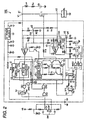
- FIG. 2 is a circuit diagram showing the arrangement of a protection apparatus for a semiconductor device including the circuit as shown in Fig. 1 .
- a protection apparatus 100 for a semiconductor device includes a switch SW1 for switching the on/off of FET (T1), a driving circuit 1, a timer 2 and a pulse counter 3.
- the protection circuit 100 further includes OR circuits OR1-OR3, AND circuits AND1-AND3 and latches DF1-DF3.
- the switch SW1 is connected to the one input terminal of the OR circuit OR2 and the other input terminal of the OR circuit OR2 is connected to the output terminal of the latch DF1.
- the output terminal of the OR circuit OR2 is connected to the one input terminal of the OR circuit OR3, and the other input terminal of the OR circuit OR3 is connected to the output terminal of the comparator CMP1.
- the output terminal of the OR circuit OR3 is connected to the driving circuit 1 and also connected to the timer 2.
- the output of the driving circuit 1 is connected to the gate of FET(T1) via the resistor R10.
- the output terminal of the comparator CMP1 is connected to the pulse counter 3.
- resistor R61, R60 and R6 are arranged in parallel to the resistor R5.
- the resistor R61 is connected to ground via a transistor T32.
- the resistor R60 is connected to ground via a transistor T31 and the resistor R6 is connected to ground via a transistor T3.
- the gate of the transistor T3 is connected to the output terminal of the timer 2.
- the gate of the transistor T31 is connected to the output terminal of the AND circuit AND3.
- the gate of the transistor T32 is connected to the output terminal of the AND circuit AND2.
- diodes D2, D3 and D4 and a resistor R30 are arranged on the input side of the amplifier AMP1.
- the driving circuit 1 supplies a driving signal to the gate of FET (T1). Then, FET (T1) turns on so that a current flows to the load RL from the power source VB to drive the load RL. Where the load RL is a lamp, the lamp is illuminated.
- the timer 2 includes an output (+Q) which is at H level for 20 ms and another output which is at H level for 200 ms.
- the 20 ms output (+Q) turns on the transistors T3, T31 and T32 so that the resistors R6, R60 and R61 are connected in parallel to the resistor R5.
- the 20 ms timer output (+Q) becomes L level so that the transistors T3, T31 and T32 turn off.
- the value of ⁇ returns to the standard value R5/R3.
- the latch DF2 is triggered so that the output (-Q) of DF2 changes from H level to L level.
- ⁇ (R5
- the latch DF3 is triggered. Therefore, if the 20 ms timer produces the third times of output et seq., only T3 turns on whereas T31 and T32 remain off.
- the number of times of outputs from the 20 ms timer is counted up by the counter 3. If it exceeds 8 (eight) times, it is decided that the circuit is in the abnormal state. Under this decision, the latch DF1 is triggered so that even if SW1 is on, FET (T1) is cut off.
- the amplifier AMP1 controls the transistor T2 so that the voltage across the resistor R3 is equal to the drain-source voltage VDS of FET (T1), the current flowing through the resistor R3 varies to increase.
- the timer 2 is triggered and the 20 ms timer output (+Q) becomes H level so that like the measure for the rush current at the start, the three transistors T32, T31 and T3 are on only for 20 ms, respectively.
- This decreases the multiplication factor of ⁇ so that the voltage V5 at the point p4 decreases and becomes lower than the voltage V4 (the case where the voltage V5 decreases but does not become lower than the voltage V4 will be described later).
- the transistors T31 and T3 turn on whereas the transistor T32 remains off because the output (-Q) of the latch DF2 is L level.
- the multiplication factor ⁇ becomes (R5
- the AND circuit AND1 output changes from L level into H level. Therefore, the latch DF1 is triggered through the OR circuit OR1 so that the DF1 output becomes H level and hence FET is cut off.
- V5 ⁇ V4 is held, the CMP1 output remains L level so that FET (T1) remains on for 20 ms.
- the latch DF3 is triggered so that the output (-Q) of the latch DF3 changes from H level to L level.
- the transistors T31, T3 turn off so that ⁇ returns to the reference value.
- V5 > V4 is held so that the 20 ms timer makes the third time start.
- the counter 3 overflows so that the latch DF1 is triggered and FET (T1) is cut off.
- the explanation hitherto made applies to the case where the abnormal state (excess current) occurs successively. However, as the case may be, the abnormal state may occur intermittently. Further, owing to malfunction, the 20 ms time may start.
- the voltage V4 is 1/ ⁇ times of that in the normal state. This is equivalent to that the cut-off current of FET (T1) has become 1/ ⁇ , thus hastening the cut-off of FET (T1).
- the voltage V5 at the point p4 increases but the voltage V4 decreases(becomes 1/ ⁇ ) so that the inversion of the comparator CMP1 is facilitated, thereby suppressing the peak value of the excess current.
- FET is caused to operate at the value not larger than the on-resistance Ron corresponding to the upper limit of the permissible channel temperature.
- This feature is realized by measuring the drain-source drop of FET (T1) which increases with an increase of Ron and by interrupting the circuit when the voltage drop reaches a prescribed level. By such a control, the channel temperature of FET (T1) does not exceed the upper limit of the permissible temperature in any case so that the semiconductor device can be surely protected.
- the elapses to interrupt the circuit depends on the magnitude of the excess current. If there occurs such excess current as twice to four times as large as the normal current (current in the normal operation), which is scarcely accompanied by the rise in the channel temperature, the circuit is designed to be interrupted after e.g. 160 ms elapses; if it is four times to eight times, interrupted after 40 ms elapses; and if it is eight times to sixteen times, interrupted after 20 ms elapses (this magnification is decided by the magnitudes of the resistors R61, R60, R6 and R5). If it is sixteen times or more (in the case of the dead short-circuiting), the circuit is interrupted after about 250 ⁇ s elapses. Therefore, the circuit can be interrupted according to the magnitude of the excess current.
- the compressing effect of the reference voltage is produced (the voltage V4 becomes 1/ ⁇ ), the device is cut off earlier so that the device and wiring can be protected.
- the cut-off current IDs and the channel heat generation ⁇ Tch are maximum. If there are changes in the on-resistance Ron 150 °C at the channel temperature of 150 °C, the characteristic of the above Equation (1) may be set using the minimum value in the changes of the on-resistance Ron.
- the on-resistance Ron 150 °C that is brought by the channel temperature of 150 °C may increase owing to an aged deterioration or an incidental deterioration, but will never decrease. In other words, we cannot estimate the upper limit of the on-resistance, but we can clearly estimate the lower limit of the on-resistance. Therefore, the maximum value of the channel heat generation ⁇ Tch that would cut off the circuit has a clear upper limit, thereby realizing the stable protection performance.
- the current detection system is a system in which as in the case of using a shunt resistance, a load current when it exceeds a prescribed current, is detected to interrupt the circuit.
- the channel heat generation ⁇ Tch increases in proportion to the on-resistance Ron.
- this change of the channel heat generation does not appear as a change in the current so that the increase in the on-resistance Ron is not detected.
- the on-resistance Ron increases, the channel heat generation further increases, which results in thermal runaway. Therefore, in the related current detection system, an excessive heating interrupting function must be incorporated separately.
- the excessive current protecting apparatus when the on-resistance Ron increases, the interrupting current value decreases so that the channel self-heating due to the increase in the on-resistance can be suppressed, which does not result in the thermal runaway. Therefore, unlike the current detection system, the excessive heating interrupting function may not be incorporated separately.
- the device is cut off before the channel temperature reaches 150 °C, the cause which gives damages to the device can be cancelled. Therefore, the occurrence of the on-mode failure of the device can be suppressed, thereby improving the reliability.
- the on-resistance Ron is small so that there is an allowance of passing a large current (even when a slight excess current occurs, the circuit can be operated without shutting off).
- the related excess current detection system a decrease in the on-resistance cannot be detected so that when the increase in the current value is detected, the circuit is interrupted regardless of the ambient temperature. Therefore, the allowance cannot be employed.
- this invention is more advantageous than the related excess current detecting system.
- FET (T1) was arranged between the plus (+) terminal of the load RL and the plus (+) terminal of the power source, but in this invention, without being limited to such an arrangement, FET (T1) can be provided on the minus (-) terminal of the load RL.
Landscapes
- Electronic Switches (AREA)
- Protection Of Static Devices (AREA)
- Emergency Protection Circuit Devices (AREA)
- Control Of Voltage And Current In General (AREA)
- Power Conversion In General (AREA)
Abstract
Claims (4)
- Procédé de protection d'un dispositif semi-conducteur (T1), comprenant les étapes consistant à :prévoir une source d'alimentation en courant continu VB, une charge (RL), et un dispositif semi-conducteur (T1) disposé entre la source d'alimentation en courant continu VB et la charge (RL) ;prévoir différents éléments de circuit connectés au dispositif semi-conducteur (T1) ;commuter le dispositif semi-conducteur (T1) de telle sorte que la charge (RL) soit basculée entre un état de marche et un état d'arrêt ;couper une conduction du dispositif semi-conducteur (T1) entre la source d'alimentation en courant continu VB et la charge (RL) lorsqu'une chute de tension aux bornes du dispositif semi-conducteur (T1) excède une tension de référence prédéterminée ; etdéfinir les constantes des différents éléments de circuit de telle sorte que la tension de référence VB/α/β ne soit pas supérieure à une tension critique,dans lequel :la tension aux bornes du dispositif semi-conducteur, multipliée par β, est comparée à la tension de la source d'alimentation en courant continu, divisée par α,la tension critique est un produit d'une résistance à l'état passant du dispositif semi-conducteur (T1), lorsque la température de son canal est à une limite supérieure de la température admissible, et d'une valeur de courant minimale qui entraîne la température du canal à atteindre la limite supérieure de la température admissible, par l'auto-échauffement dû à l'effet Joule.
- Procédé selon la revendication 1, dans lequel, lorsqu'il y a des changements de la résistance à l'état passant pour la spécification du dispositif semi-conducteur (T1), c'est la valeur minimale parmi les changements de la résistance à l'état passant qui est utilisée pour déterminer la tension critique.
- Appareil de protection pour un dispositif semi-conducteur (T1), comprenant :- une source d'alimentation en courant continu VB ;- une charge (RL) ;- un dispositif semi-conducteur (T1), disposé entre la source d'alimentation en courant continu et la charge, et qui fait basculer la charge entre un état de marche et un état d'arrêt ;différents éléments de circuit connectés au dispositif semi-conducteur ;
une section de coupure, coupant une conduction du dispositif semi-conducteur entre la source d'alimentation en courant continu et la charge lorsque lorsqu'une chute de tension aux bornes du dispositif semi-conducteur est supérieure à une tension de référence prédéterminée ;
où les constantes des différents éléments de circuit sont définies de telle sorte que la tension de référence VB/α/β ne soit pas supérieure à une tension critique ;
un comparateur (CMP1), comparant la chute de tension à la tension de référence prédéterminée en comparant une chute de tension aux bornes du dispositif semi-conducteur, multipliée par β, à la tension de la source d'alimentation en courant continu, divisée par α ; et
où la tension critique est un produit d'une résistance à l'état passant du dispositif semi-conducteur, lorsque la température de son canal est à une limite supérieure de la température admissible, et d'une valeur de courant minimale qui entraîne la température du canal à atteindre la limite supérieure de la température admissible, par l'auto-échauffement dû à l'effet Joule. - Appareil de protection selon la revendication 3, dans lequel, lorsqu'il y a des changements de la résistance à l'état passant pour la spécification du dispositif semi-conducteur (T1), c'est la valeur minimale parmi les changements de la résistance à l'état passant qui est utilisée pour déterminer la tension critique.
Applications Claiming Priority (3)
| Application Number | Priority Date | Filing Date | Title |
|---|---|---|---|
| JP2002204729A JP3990218B2 (ja) | 2002-07-12 | 2002-07-12 | 半導体素子の保護装置 |
| JP2002204729 | 2002-07-12 | ||
| PCT/JP2003/008786 WO2004008500A2 (fr) | 2002-07-12 | 2003-07-10 | Procede de protection de dispositif semi-conducteur et appareil de protection de dispositif semi-conducteur l'utilisant |
Publications (2)
| Publication Number | Publication Date |
|---|---|
| EP1522089A2 EP1522089A2 (fr) | 2005-04-13 |
| EP1522089B1 true EP1522089B1 (fr) | 2011-03-30 |
Family
ID=30112732
Family Applications (1)
| Application Number | Title | Priority Date | Filing Date |
|---|---|---|---|
| EP03764163A Expired - Lifetime EP1522089B1 (fr) | 2002-07-12 | 2003-07-10 | Procede de protection de dispositif semi-conducteur et appareil de protection de dispositif semi-conducteur l'utilisant |
Country Status (8)
| Country | Link |
|---|---|
| US (1) | US7248452B2 (fr) |
| EP (1) | EP1522089B1 (fr) |
| JP (2) | JP3990218B2 (fr) |
| KR (1) | KR100749181B1 (fr) |
| CN (1) | CN1669118B (fr) |
| AU (1) | AU2003250532A1 (fr) |
| DE (1) | DE60336560D1 (fr) |
| WO (1) | WO2004008500A2 (fr) |
Families Citing this family (18)
| Publication number | Priority date | Publication date | Assignee | Title |
|---|---|---|---|---|
| JP4278572B2 (ja) * | 2004-06-16 | 2009-06-17 | 矢崎総業株式会社 | 半導体スイッチの制御装置 |
| JP4398312B2 (ja) * | 2004-07-06 | 2010-01-13 | 矢崎総業株式会社 | 半導体スイッチの制御装置 |
| JP4701052B2 (ja) | 2005-09-21 | 2011-06-15 | 矢崎総業株式会社 | 過電流検出装置 |
| JP4773822B2 (ja) * | 2005-12-26 | 2011-09-14 | 株式会社オートネットワーク技術研究所 | 電力供給制御装置 |
| JP4800772B2 (ja) * | 2006-01-04 | 2011-10-26 | ルネサスエレクトロニクス株式会社 | 過電流検出回路 |
| JP4929020B2 (ja) | 2007-04-10 | 2012-05-09 | 矢崎総業株式会社 | 負荷回路の過電流保護装置 |
| JP5030717B2 (ja) * | 2007-09-10 | 2012-09-19 | 矢崎総業株式会社 | 過電流保護装置 |
| US7843248B1 (en) * | 2007-11-01 | 2010-11-30 | Intersil Americas Inc. | Analog switch with overcurrent detection |
| JP5087441B2 (ja) * | 2008-03-19 | 2012-12-05 | 矢崎総業株式会社 | 電力供給装置 |
| JP5351694B2 (ja) * | 2009-10-02 | 2013-11-27 | 矢崎総業株式会社 | 半導体スイッチの保護装置 |
| JP2011130564A (ja) * | 2009-12-17 | 2011-06-30 | Hitachi Ltd | パワー半導体スイッチ素子の保護装置および保護方法 |
| JP5351793B2 (ja) * | 2010-02-05 | 2013-11-27 | 矢崎総業株式会社 | 過電流保護装置及び過電流保護システム |
| JP5480653B2 (ja) * | 2010-02-05 | 2014-04-23 | 矢崎総業株式会社 | 負荷回路の過電流保護装置 |
| JP5952060B2 (ja) * | 2012-04-05 | 2016-07-13 | 矢崎総業株式会社 | 発熱保護回路及び発熱保護方法 |
| JP6164429B2 (ja) | 2012-05-01 | 2017-07-19 | 大島俊蔵 | 過電流保護電源装置 |
| JP6597213B2 (ja) * | 2015-11-12 | 2019-10-30 | 株式会社デンソー | 過電流検出装置 |
| WO2017134824A1 (fr) | 2016-02-05 | 2017-08-10 | 俊蔵 大島 | Dispositif d'alimentation électrique |
| JP7347316B2 (ja) * | 2020-04-20 | 2023-09-20 | 株式会社オートネットワーク技術研究所 | 給電制御装置 |
Citations (1)
| Publication number | Priority date | Publication date | Assignee | Title |
|---|---|---|---|---|
| JP2002017036A (ja) * | 2000-06-29 | 2002-01-18 | Nissan Motor Co Ltd | 過電流検知回路 |
Family Cites Families (26)
| Publication number | Priority date | Publication date | Assignee | Title |
|---|---|---|---|---|
| JPH056053Y2 (fr) | 1987-07-22 | 1993-02-17 | ||
| JP2797336B2 (ja) | 1988-09-26 | 1998-09-17 | 日本電気株式会社 | 半導体集積回路 |
| JPH06180332A (ja) | 1992-12-14 | 1994-06-28 | Nec Kansai Ltd | 電流検出回路 |
| JP2779373B2 (ja) | 1993-03-29 | 1998-07-23 | セイコープレシジョン株式会社 | El素子 |
| JP3080823B2 (ja) | 1993-10-15 | 2000-08-28 | モトローラ株式会社 | 半導体集積回路装置 |
| EP0877473B1 (fr) * | 1994-06-10 | 2005-01-12 | Omron Corporation | Circuit de commande pour moteur à courant continue |
| JPH0870244A (ja) | 1994-08-30 | 1996-03-12 | Hitachi Ltd | 駆動回路 |
| US5563759A (en) | 1995-04-11 | 1996-10-08 | International Rectifier Corporation | Protected three-pin mosgated power switch with separate input reset signal level |
| DE69522097T2 (de) | 1995-05-31 | 2002-04-18 | Co.Ri.M.Me. Consorzio Per La Ricerca Sulla Microelettronica Nel Mezzogiorno, Catania | Schaltung zum Erkennen von und Schutz vor Kurzschlüssen für digitale Ausgänge |
| JPH09145749A (ja) | 1995-11-29 | 1997-06-06 | Toyota Motor Corp | 電流検出回路 |
| JP2940542B2 (ja) * | 1997-05-07 | 1999-08-25 | セイコーエプソン株式会社 | インクジェット式プリントヘッドの駆動波形生成装置及び駆動波形生成方法 |
| JPH10335998A (ja) | 1997-06-05 | 1998-12-18 | Denso Corp | 電流検出回路 |
| DE19729904A1 (de) | 1997-07-12 | 1999-02-11 | Kammerer Gmbh M | Schaltungsanordnung zur Überwachung von durch eine Last fließenden Strömen |
| JP3706515B2 (ja) * | 1998-12-28 | 2005-10-12 | 矢崎総業株式会社 | 電源供給制御装置および電源供給制御方法 |
| JP2000235424A (ja) | 1999-02-12 | 2000-08-29 | Yazaki Corp | カレントミラー回路、電流センサ及びこれを具備したスイッチング回路並びにスイッチングデバイス |
| JP2000299922A (ja) * | 1999-02-12 | 2000-10-24 | Yazaki Corp | 電源供給制御装置および電源供給制御方法 |
| JP3509605B2 (ja) | 1999-02-12 | 2004-03-22 | 日信工業株式会社 | 電気機器駆動回路における電界効果トランジスタの過熱診断装置 |
| JP2000308340A (ja) | 1999-02-19 | 2000-11-02 | Yazaki Corp | ヒューズレスdc/dcコンバータ |
| JP2000350440A (ja) | 1999-06-01 | 2000-12-15 | Murata Mfg Co Ltd | 降圧型スイッチング電源回路 |
| JP4355463B2 (ja) | 1999-06-18 | 2009-11-04 | パナソニック株式会社 | 出力制御装置 |
| US6166530A (en) * | 2000-02-11 | 2000-12-26 | Advanced Analogic Technologies, Inc. | Current-Limited switch with fast transient response |
| US6377032B1 (en) * | 2000-07-20 | 2002-04-23 | Semtech Corporation | Method and apparatus for virtual current sensing in DC-DC switched mode power supplies |
| JP3741949B2 (ja) * | 2000-07-24 | 2006-02-01 | 矢崎総業株式会社 | 半導体スイッチング装置 |
| JP3914004B2 (ja) * | 2001-05-25 | 2007-05-16 | 矢崎総業株式会社 | 半導体素子の過電流検出・保護装置 |
| US6552889B1 (en) * | 2001-07-17 | 2003-04-22 | Vishay Siliconix | Current limiting technique for hybrid power MOSFET circuits |
| US6624994B1 (en) * | 2001-11-09 | 2003-09-23 | National Semiconductor Corporation | Apparatus and method for over-current protection of an analog switch |
-
2002
- 2002-07-12 JP JP2002204729A patent/JP3990218B2/ja not_active Expired - Fee Related
-
2003
- 2003-07-10 CN CN038164655A patent/CN1669118B/zh not_active Expired - Fee Related
- 2003-07-10 AU AU2003250532A patent/AU2003250532A1/en not_active Abandoned
- 2003-07-10 DE DE60336560T patent/DE60336560D1/de not_active Expired - Lifetime
- 2003-07-10 EP EP03764163A patent/EP1522089B1/fr not_active Expired - Lifetime
- 2003-07-10 US US10/519,745 patent/US7248452B2/en not_active Expired - Fee Related
- 2003-07-10 WO PCT/JP2003/008786 patent/WO2004008500A2/fr not_active Ceased
- 2003-07-10 KR KR1020047021572A patent/KR100749181B1/ko not_active Expired - Fee Related
-
2007
- 2007-01-22 JP JP2007011932A patent/JP2007159159A/ja not_active Abandoned
Patent Citations (1)
| Publication number | Priority date | Publication date | Assignee | Title |
|---|---|---|---|---|
| JP2002017036A (ja) * | 2000-06-29 | 2002-01-18 | Nissan Motor Co Ltd | 過電流検知回路 |
Also Published As
| Publication number | Publication date |
|---|---|
| CN1669118B (zh) | 2010-10-06 |
| EP1522089A2 (fr) | 2005-04-13 |
| AU2003250532A1 (en) | 2004-02-02 |
| KR20050016677A (ko) | 2005-02-21 |
| US20050275990A1 (en) | 2005-12-15 |
| CN1669118A (zh) | 2005-09-14 |
| KR100749181B1 (ko) | 2007-08-13 |
| US7248452B2 (en) | 2007-07-24 |
| JP2007159159A (ja) | 2007-06-21 |
| WO2004008500A2 (fr) | 2004-01-22 |
| JP2004048498A (ja) | 2004-02-12 |
| JP3990218B2 (ja) | 2007-10-10 |
| DE60336560D1 (de) | 2011-05-12 |
| WO2004008500A3 (fr) | 2004-05-21 |
Similar Documents
| Publication | Publication Date | Title |
|---|---|---|
| EP1522089B1 (fr) | Procede de protection de dispositif semi-conducteur et appareil de protection de dispositif semi-conducteur l'utilisant | |
| EP2139115A1 (fr) | Protecteur de surintensité pour circuit de charge | |
| EP0402928B1 (fr) | Circuit interne pour limiter le courant pour un disjoncteur rapide | |
| US4800331A (en) | Linear current limiter with temperature shutdown | |
| US8315028B2 (en) | Overcurrent protection apparatus | |
| US8054602B2 (en) | Power supply controller | |
| US8270138B2 (en) | Power supply controller and threshold adjustment method thereof | |
| US8598859B2 (en) | Power supply controller | |
| JP4398312B2 (ja) | 半導体スイッチの制御装置 | |
| EP1770863B1 (fr) | Dispositif de protection contre surintensité | |
| EP3667849B1 (fr) | Systèmes et procédés pour la protection contre la foudre dans des modules de distribution d'énergie | |
| EP2293442A1 (fr) | Dispositif de protection contre les surintensités pour un circuit de charge | |
| JPH0526912A (ja) | 過電流検出回路 | |
| JP3812334B2 (ja) | 直流負荷駆動装置 | |
| US7369387B2 (en) | Apparatus and method for temperature-dependent transient blocking | |
| DE102019103615A1 (de) | Kurzschlussschutz für einen gatetreiber unter verwendung eines gepulsten betriebs | |
| EP0397017B1 (fr) | Dispositif pour la protection de circuits semi-conducteurs contre des transitoires sur la ligne d'alimentation | |
| US7777532B2 (en) | Method and circuit for protecting a MOSFET | |
| JP2001189650A (ja) | 半導体リレー | |
| JP2005129697A (ja) | 半導体素子の温度監視装置 | |
| JPH09135156A (ja) | 電気負荷の駆動装置 | |
| JP2000312140A (ja) | 電源供給制御装置 | |
| JPH04269555A (ja) | プリンタドライブ回路の過電流検出装置 |
Legal Events
| Date | Code | Title | Description |
|---|---|---|---|
| PUAI | Public reference made under article 153(3) epc to a published international application that has entered the european phase |
Free format text: ORIGINAL CODE: 0009012 |
|
| 17P | Request for examination filed |
Effective date: 20050105 |
|
| AK | Designated contracting states |
Kind code of ref document: A2 Designated state(s): AT BE BG CH CY CZ DE DK EE ES FI FR GB GR HU IE IT LI LU MC NL PT RO SE SI SK TR |
|
| RBV | Designated contracting states (corrected) |
Designated state(s): DE FR GB |
|
| 17Q | First examination report despatched |
Effective date: 20090209 |
|
| GRAP | Despatch of communication of intention to grant a patent |
Free format text: ORIGINAL CODE: EPIDOSNIGR1 |
|
| GRAS | Grant fee paid |
Free format text: ORIGINAL CODE: EPIDOSNIGR3 |
|
| GRAA | (expected) grant |
Free format text: ORIGINAL CODE: 0009210 |
|
| AK | Designated contracting states |
Kind code of ref document: B1 Designated state(s): DE FR GB |
|
| REG | Reference to a national code |
Ref country code: GB Ref legal event code: FG4D |
|
| REF | Corresponds to: |
Ref document number: 60336560 Country of ref document: DE Date of ref document: 20110512 Kind code of ref document: P |
|
| REG | Reference to a national code |
Ref country code: DE Ref legal event code: R096 Ref document number: 60336560 Country of ref document: DE Effective date: 20110512 |
|
| PLBE | No opposition filed within time limit |
Free format text: ORIGINAL CODE: 0009261 |
|
| STAA | Information on the status of an ep patent application or granted ep patent |
Free format text: STATUS: NO OPPOSITION FILED WITHIN TIME LIMIT |
|
| 26N | No opposition filed |
Effective date: 20120102 |
|
| REG | Reference to a national code |
Ref country code: DE Ref legal event code: R097 Ref document number: 60336560 Country of ref document: DE Effective date: 20120102 |
|
| REG | Reference to a national code |
Ref country code: FR Ref legal event code: PLFP Year of fee payment: 13 |
|
| PGFP | Annual fee paid to national office [announced via postgrant information from national office to epo] |
Ref country code: GB Payment date: 20150708 Year of fee payment: 13 Ref country code: DE Payment date: 20150707 Year of fee payment: 13 |
|
| PGFP | Annual fee paid to national office [announced via postgrant information from national office to epo] |
Ref country code: FR Payment date: 20150629 Year of fee payment: 13 |
|
| REG | Reference to a national code |
Ref country code: DE Ref legal event code: R119 Ref document number: 60336560 Country of ref document: DE |
|
| GBPC | Gb: european patent ceased through non-payment of renewal fee |
Effective date: 20160710 |
|
| PG25 | Lapsed in a contracting state [announced via postgrant information from national office to epo] |
Ref country code: FR Free format text: LAPSE BECAUSE OF NON-PAYMENT OF DUE FEES Effective date: 20160801 Ref country code: DE Free format text: LAPSE BECAUSE OF NON-PAYMENT OF DUE FEES Effective date: 20170201 |
|
| REG | Reference to a national code |
Ref country code: FR Ref legal event code: ST Effective date: 20170331 |
|
| PG25 | Lapsed in a contracting state [announced via postgrant information from national office to epo] |
Ref country code: GB Free format text: LAPSE BECAUSE OF NON-PAYMENT OF DUE FEES Effective date: 20160710 |