EP1511884B1 - Vorrichtung und verfahren zur herstellung von einkristallinem siliziumkarbid - Google Patents
Vorrichtung und verfahren zur herstellung von einkristallinem siliziumkarbid Download PDFInfo
- Publication number
- EP1511884B1 EP1511884B1 EP03752816A EP03752816A EP1511884B1 EP 1511884 B1 EP1511884 B1 EP 1511884B1 EP 03752816 A EP03752816 A EP 03752816A EP 03752816 A EP03752816 A EP 03752816A EP 1511884 B1 EP1511884 B1 EP 1511884B1
- Authority
- EP
- European Patent Office
- Prior art keywords
- enclosure
- substrate
- compound
- polycrystalline
- source
- Prior art date
- Legal status (The legal status is an assumption and is not a legal conclusion. Google has not performed a legal analysis and makes no representation as to the accuracy of the status listed.)
- Expired - Lifetime
Links
- HBMJWWWQQXIZIP-UHFFFAOYSA-N silicon carbide Chemical compound [Si+]#[C-] HBMJWWWQQXIZIP-UHFFFAOYSA-N 0.000 title claims description 59
- 229910021421 monocrystalline silicon Inorganic materials 0.000 title claims description 6
- 230000015572 biosynthetic process Effects 0.000 title description 7
- 239000000758 substrate Substances 0.000 claims abstract description 41
- 238000000859 sublimation Methods 0.000 claims abstract description 26
- 230000008022 sublimation Effects 0.000 claims abstract description 26
- 150000001875 compounds Chemical class 0.000 claims abstract description 19
- 239000002243 precursor Substances 0.000 claims abstract description 13
- 239000013078 crystal Substances 0.000 claims abstract description 12
- 230000008021 deposition Effects 0.000 claims abstract description 7
- 230000008020 evaporation Effects 0.000 claims abstract description 6
- 238000001704 evaporation Methods 0.000 claims abstract description 6
- 238000010438 heat treatment Methods 0.000 claims abstract description 6
- 229910010271 silicon carbide Inorganic materials 0.000 claims description 52
- 239000007789 gas Substances 0.000 claims description 17
- 238000000034 method Methods 0.000 claims description 14
- 230000006698 induction Effects 0.000 claims description 6
- 238000000151 deposition Methods 0.000 claims description 5
- 238000009792 diffusion process Methods 0.000 claims description 3
- 238000009833 condensation Methods 0.000 claims description 2
- 230000005494 condensation Effects 0.000 claims description 2
- 238000005229 chemical vapour deposition Methods 0.000 claims 1
- OKTJSMMVPCPJKN-UHFFFAOYSA-N Carbon Chemical compound [C] OKTJSMMVPCPJKN-UHFFFAOYSA-N 0.000 description 12
- 238000004519 manufacturing process Methods 0.000 description 10
- 239000000843 powder Substances 0.000 description 10
- 229910002804 graphite Inorganic materials 0.000 description 8
- 239000010439 graphite Substances 0.000 description 8
- XKRFYHLGVUSROY-UHFFFAOYSA-N Argon Chemical compound [Ar] XKRFYHLGVUSROY-UHFFFAOYSA-N 0.000 description 4
- ATUOYWHBWRKTHZ-UHFFFAOYSA-N Propane Chemical compound CCC ATUOYWHBWRKTHZ-UHFFFAOYSA-N 0.000 description 4
- 229910052799 carbon Inorganic materials 0.000 description 4
- 125000006850 spacer group Chemical group 0.000 description 4
- 239000012159 carrier gas Substances 0.000 description 3
- 230000000295 complement effect Effects 0.000 description 3
- 230000007935 neutral effect Effects 0.000 description 3
- 229910052710 silicon Inorganic materials 0.000 description 3
- 239000010703 silicon Substances 0.000 description 3
- 238000005092 sublimation method Methods 0.000 description 3
- 238000007740 vapor deposition Methods 0.000 description 3
- 238000005019 vapor deposition process Methods 0.000 description 3
- BLRPTPMANUNPDV-UHFFFAOYSA-N Silane Chemical compound [SiH4] BLRPTPMANUNPDV-UHFFFAOYSA-N 0.000 description 2
- 229910052786 argon Inorganic materials 0.000 description 2
- 239000002019 doping agent Substances 0.000 description 2
- 239000001294 propane Substances 0.000 description 2
- 229910000077 silane Inorganic materials 0.000 description 2
- ZAMOUSCENKQFHK-UHFFFAOYSA-N Chlorine atom Chemical compound [Cl] ZAMOUSCENKQFHK-UHFFFAOYSA-N 0.000 description 1
- UFHFLCQGNIYNRP-UHFFFAOYSA-N Hydrogen Chemical compound [H][H] UFHFLCQGNIYNRP-UHFFFAOYSA-N 0.000 description 1
- 229910003902 SiCl 4 Inorganic materials 0.000 description 1
- 238000006243 chemical reaction Methods 0.000 description 1
- 239000000460 chlorine Substances 0.000 description 1
- 229910052801 chlorine Inorganic materials 0.000 description 1
- 238000002485 combustion reaction Methods 0.000 description 1
- PMHQVHHXPFUNSP-UHFFFAOYSA-M copper(1+);methylsulfanylmethane;bromide Chemical compound Br[Cu].CSC PMHQVHHXPFUNSP-UHFFFAOYSA-M 0.000 description 1
- 238000002425 crystallisation Methods 0.000 description 1
- 230000008025 crystallization Effects 0.000 description 1
- 230000007547 defect Effects 0.000 description 1
- 238000009826 distribution Methods 0.000 description 1
- 239000001257 hydrogen Substances 0.000 description 1
- 229910052739 hydrogen Inorganic materials 0.000 description 1
- 239000012535 impurity Substances 0.000 description 1
- 239000000463 material Substances 0.000 description 1
- VNWKTOKETHGBQD-UHFFFAOYSA-N methane Chemical compound C VNWKTOKETHGBQD-UHFFFAOYSA-N 0.000 description 1
- 238000004377 microelectronic Methods 0.000 description 1
- 239000000203 mixture Substances 0.000 description 1
- 238000012986 modification Methods 0.000 description 1
- 230000004048 modification Effects 0.000 description 1
- 230000005693 optoelectronics Effects 0.000 description 1
- 229910021420 polycrystalline silicon Inorganic materials 0.000 description 1
- 238000002360 preparation method Methods 0.000 description 1
- 239000000126 substance Substances 0.000 description 1
- 239000012808 vapor phase Substances 0.000 description 1
Images

Classifications
-
- C—CHEMISTRY; METALLURGY
- C30—CRYSTAL GROWTH
- C30B—SINGLE-CRYSTAL GROWTH; UNIDIRECTIONAL SOLIDIFICATION OF EUTECTIC MATERIAL OR UNIDIRECTIONAL DEMIXING OF EUTECTOID MATERIAL; REFINING BY ZONE-MELTING OF MATERIAL; PRODUCTION OF A HOMOGENEOUS POLYCRYSTALLINE MATERIAL WITH DEFINED STRUCTURE; SINGLE CRYSTALS OR HOMOGENEOUS POLYCRYSTALLINE MATERIAL WITH DEFINED STRUCTURE; AFTER-TREATMENT OF SINGLE CRYSTALS OR A HOMOGENEOUS POLYCRYSTALLINE MATERIAL WITH DEFINED STRUCTURE; APPARATUS THEREFOR
- C30B23/00—Single-crystal growth by condensing evaporated or sublimed materials
- C30B23/002—Controlling or regulating
- C30B23/005—Controlling or regulating flux or flow of depositing species or vapour
-
- C—CHEMISTRY; METALLURGY
- C30—CRYSTAL GROWTH
- C30B—SINGLE-CRYSTAL GROWTH; UNIDIRECTIONAL SOLIDIFICATION OF EUTECTIC MATERIAL OR UNIDIRECTIONAL DEMIXING OF EUTECTOID MATERIAL; REFINING BY ZONE-MELTING OF MATERIAL; PRODUCTION OF A HOMOGENEOUS POLYCRYSTALLINE MATERIAL WITH DEFINED STRUCTURE; SINGLE CRYSTALS OR HOMOGENEOUS POLYCRYSTALLINE MATERIAL WITH DEFINED STRUCTURE; AFTER-TREATMENT OF SINGLE CRYSTALS OR A HOMOGENEOUS POLYCRYSTALLINE MATERIAL WITH DEFINED STRUCTURE; APPARATUS THEREFOR
- C30B23/00—Single-crystal growth by condensing evaporated or sublimed materials
-
- C—CHEMISTRY; METALLURGY
- C30—CRYSTAL GROWTH
- C30B—SINGLE-CRYSTAL GROWTH; UNIDIRECTIONAL SOLIDIFICATION OF EUTECTIC MATERIAL OR UNIDIRECTIONAL DEMIXING OF EUTECTOID MATERIAL; REFINING BY ZONE-MELTING OF MATERIAL; PRODUCTION OF A HOMOGENEOUS POLYCRYSTALLINE MATERIAL WITH DEFINED STRUCTURE; SINGLE CRYSTALS OR HOMOGENEOUS POLYCRYSTALLINE MATERIAL WITH DEFINED STRUCTURE; AFTER-TREATMENT OF SINGLE CRYSTALS OR A HOMOGENEOUS POLYCRYSTALLINE MATERIAL WITH DEFINED STRUCTURE; APPARATUS THEREFOR
- C30B23/00—Single-crystal growth by condensing evaporated or sublimed materials
- C30B23/02—Epitaxial-layer growth
-
- C—CHEMISTRY; METALLURGY
- C30—CRYSTAL GROWTH
- C30B—SINGLE-CRYSTAL GROWTH; UNIDIRECTIONAL SOLIDIFICATION OF EUTECTIC MATERIAL OR UNIDIRECTIONAL DEMIXING OF EUTECTOID MATERIAL; REFINING BY ZONE-MELTING OF MATERIAL; PRODUCTION OF A HOMOGENEOUS POLYCRYSTALLINE MATERIAL WITH DEFINED STRUCTURE; SINGLE CRYSTALS OR HOMOGENEOUS POLYCRYSTALLINE MATERIAL WITH DEFINED STRUCTURE; AFTER-TREATMENT OF SINGLE CRYSTALS OR A HOMOGENEOUS POLYCRYSTALLINE MATERIAL WITH DEFINED STRUCTURE; APPARATUS THEREFOR
- C30B29/00—Single crystals or homogeneous polycrystalline material with defined structure characterised by the material or by their shape
- C30B29/10—Inorganic compounds or compositions
- C30B29/36—Carbides
-
- Y—GENERAL TAGGING OF NEW TECHNOLOGICAL DEVELOPMENTS; GENERAL TAGGING OF CROSS-SECTIONAL TECHNOLOGIES SPANNING OVER SEVERAL SECTIONS OF THE IPC; TECHNICAL SUBJECTS COVERED BY FORMER USPC CROSS-REFERENCE ART COLLECTIONS [XRACs] AND DIGESTS
- Y10—TECHNICAL SUBJECTS COVERED BY FORMER USPC
- Y10T—TECHNICAL SUBJECTS COVERED BY FORMER US CLASSIFICATION
- Y10T117/00—Single-crystal, oriented-crystal, and epitaxy growth processes; non-coating apparatus therefor
- Y10T117/10—Apparatus
-
- Y—GENERAL TAGGING OF NEW TECHNOLOGICAL DEVELOPMENTS; GENERAL TAGGING OF CROSS-SECTIONAL TECHNOLOGIES SPANNING OVER SEVERAL SECTIONS OF THE IPC; TECHNICAL SUBJECTS COVERED BY FORMER USPC CROSS-REFERENCE ART COLLECTIONS [XRACs] AND DIGESTS
- Y10—TECHNICAL SUBJECTS COVERED BY FORMER USPC
- Y10T—TECHNICAL SUBJECTS COVERED BY FORMER US CLASSIFICATION
- Y10T117/00—Single-crystal, oriented-crystal, and epitaxy growth processes; non-coating apparatus therefor
- Y10T117/10—Apparatus
- Y10T117/1004—Apparatus with means for measuring, testing, or sensing
- Y10T117/1008—Apparatus with means for measuring, testing, or sensing with responsive control means
Definitions
- the present invention relates to a method and a device for forming in monocrystalline form a compound body with non-congruent evaporation which can exist in monocrystalline or polycrystalline form.
- the remainder of the description will apply, by way of example, to the formation of monocrystalline silicon carbide, SiC.
- the invention applies in particular to the production of ingots or thick layers of monocrystalline SiC of a type of crystallization, for example, cubic or hexagonal.
- Such ingots or thick layers can be used for the manufacture of substrates or active layers usable in microelectronics.
- the monocrystalline SiC must have good crystal quality and a perfectly controlled dopant level.
- a first known method for the production of electron quality single crystal SiC ingots is based on the sublimation of an SiC powder and the condensation of the vapors formed on a monocrystalline SiC seed.
- a device for carrying out such a method generally comprises a graphite crucible which defines a sublimation chamber in which the monocrystalline seed is placed from which it is desired to form an ingot of SiC and the powder SiC which is the source of SiC.
- the SiC powder and the seed are respectively heated at temperatures T 1 and T 2 such that T 1 is greater than T 2 .
- the impurities contained in the SiC powder are at the origin of defects and undesirable doping of the monocrystal obtained.
- the sublimation process does not allow the growth of monocrystalline crystals of large size because of the necessarily limited quantity of powder constituting the source of SiC. Indeed, it is in practice impossible to feed the crucible in powder of SiC continuously without unduly disturbing the growth conditions of monocrystalline SiC. In addition, it is also not possible to have a large amount of powder in the crucible. Indeed, the sublimation of SiC is not congruent and it appears that a larger amount of silicon than carbon is produced during the sublimation of the powder. The powder therefore tends to charge in carbon. Finally, as the course of the process progresses, a change in the composition of the powder and the vapors resulting from the sublimation is obtained, and consequently a change in the growth conditions of the monocrystal.
- a second method of manufacturing monocrystalline SiC ingots consists of a very high temperature vapor deposition (HTCVD) of SiC on a monocrystalline SiC seed.
- HTCVD very high temperature vapor deposition
- gaseous precursors of silicon and carbon for example silane and propane, are sent, optionally with the aid of a carrier gas, to the seed and react for form on the seed a monocrystalline SiC deposit.
- the vapor deposition process is also used for producing active layers.
- the main disadvantage of the vapor deposition process lies in the extreme difficulty in controlling the growth of the monocrystalline ingot, in particular because of the turbulent movements of the gaseous precursors.
- the vapor deposition process does not allow to exceed deposit rates of the order of two or three tens of micrometers per hour.
- EP-A-0554047 and WO-A-97/13012 teaches devices and methods for formation of monocrystalline silicon carbide in a two-step method, i.e., a CVD step to form the SiC source followed by a sublimation step of that source to form the SiC monocrystalline.
- the present invention aims to obtain a single crystal SiC formation process on a monocrystalline SiC seed does not have the disadvantages of previously described methods.
- the present invention also aims to obtain a device for the manufacture of active layers up to a thickness greater than a few tens of micrometers or monocrystalline SiC ingots.
- the present invention provides a device for forming in the monocrystalline state a compound body with non-congruent evaporation, capable of existing in monocrystalline or polycrystalline form, comprising a first chamber containing a substrate at which is formed a polycrystalline source of said body and a monocrystalline seed of said body; a second enclosure, said substrate being disposed between the two enclosures; means for supplying gaseous precursors of said body into the second chamber capable of causing the deposition of said body in polycrystalline form on the substrate; and heating means for maintaining the substrate at a temperature above the temperature of the seed so as to cause the sublimation of the polycrystalline source and the deposition on the seed of said body in monocrystalline form.
- said body is silicon carbide.
- the first chamber is defined by a first cylindrical wall, a lid, on which is fixed the germ, covering at least in part an end of the first wall, and the substrate covering at least partly the opposite end of the first wall, said substrate being permeable.
- the second enclosure is defined by a second cylindrical wall disposed in the extension of the first cylindrical wall on the substrate side.
- the first and second cylindrical walls are surrounded by a tube which delimits with the first and second cylindrical walls a tubular recess, the second chamber communicating with said tubular recess.
- the device comprises means for producing a gas flow in the tubular recess for evacuating gases present in the second enclosure.
- the heating means comprise at least one induction coil surrounding the tube and traversed by an alternating current so as to induce induction currents only in the tube.
- the lid is mounted to move in translation relative to the first cylindrical wall along the axis of the first cylindrical wall.
- the present invention also provides a method for forming in the monocrystalline state a compound body with non-congruent evaporation capable of existing in monocrystalline or polycrystalline form, comprising the steps carried out simultaneously consisting of forming on a permeable substrate, arranged between first and second and second enclosures, a source of said body in polycrystalline form by vapor deposition of gaseous precursors of said body supplying the second enclosure; forming in the first chamber gaseous bodies by sublimation of a part of the source; and forming said body in monocrystalline form by condensing the gaseous bodies on a seed disposed in the first enclosure.
- the seed is removed from the substrate as and when the formation of monocrystalline silicon carbide.
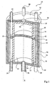
- the figure 1 represents a device 10 consisting of a first cylindrical wall 12 made of Z-axis graphite defining a first enclosure 14, hereinafter referred to as a supply enclosure.
- the second cylindrical wall 16 is disposed in the extension of the first cylindrical wall 12 and is separated from the latter by spacers 22, a single spacer being shown on the figure 1 .
- the spacers 22 delimit a substantially annular passage 24 between the two enclosures 14, 20.
- the axis Z corresponds for example to the vertical axis, the sublimation chamber 20 being disposed above the feed enclosure 14.
- a cylindrical tube 26 of Z-axis graphite surrounds the two cylindrical walls 12, 16 and delimits therewith a tubular recess 28.
- the two enclosures 14, 20 are enclosed in an insulating housing 29 of graphite felt consisting of a wall cylindrical axis Z disposed around the tube 26 and closed at both ends by substantially circular plates 32, 34.
- a gas supply duct 36 communicates with the supply chamber 14 through the plate 34.
- Supply ducts 38 of a neutral gas communicate with the tubular recess 28 through the plate 34 on the other side. of the supply enclosure 14.
- Gas discharge lines 40 communicate with the tubular recess 28 through the plate 32.
- a circular substrate 42 for example made of porous carbon foam or sintered SiC, is placed on a washer 44 held against the cylindrical wall 16 by the spacers 22.
- the diameter of the substrate 42 corresponds for example substantially to the inside diameter of the cylindrical wall 16.
- the diameter of the substrate 42 may, however, be smaller than the inside diameter of the cylindrical wall 16, and the supply enclosure 14 may optionally partially communicate directly with the sublimation chamber 20.
- the substrate 42 separates the sublimation chamber
- the substrate 42 is permeable to gases from sublimation of the SiC or at least allows diffusion there through polycrystalline SiC.
- a seed 46 of monocrystalline silicon carbide is placed in the sublimation chamber 20 on the cover 18.
- An opening 50 is made in the circular plate 32 and discovers a portion of the cover 18 at the level of the seed 46.
- Induction turns surround the cylindrical wall 30 of the insulating housing 29 substantially at the substrate 42.
- the frequency of the current feeding the induction turns is such that only the tube 26 is traversed by induced currents.
- the distribution of temperatures in the chambers 14, 20 heated by the tube 26 is then substantially independent of the materials present in the enclosures 14, 20 and therefore chemical phenomena occurring in the enclosures 14 and 20.
- the SiC manufacturing process according to the invention is as follows.
- the device 10 is placed in a chamber under a partial vacuum, or in an inert atmosphere to prevent any combustion reaction of the graphite constituting the device.
- a temperature gradient is imposed inside the sublimation chamber 20 between the substrate 42 and the seed 46 such that the temperature T 1 of the substrate 42 is greater than the temperature T 2 of the seed 46.
- the temperature T 1 is for example between 2000 ° C and 2400 ° C
- the temperature T 2 is for example between 1900 ° C and 2200 ° C.
- the insulating housing 29 limits heat loss.
- the opening 50 in the insulating housing 29 promotes the temperature drop of the seed 46.
- a neutral gas such as argon
- gaseous precursors of silicon and carbon reacting at high temperature are introduced into the supply enclosure 14 and directed towards the substrate 42.
- the gaseous precursors are optionally mixed with one or more carrier gases. for example argon or hydrogen.
- Gaseous precursors for example silane, propane or chlorine-based gases, for example SiCl 4 , react at a very high temperature to form polycrystalline SiC on the substrate 42.
- the gaseous precursors, having totally or partially reacted, and the The carrier gas 14 is then discharged from the supply chamber 14 through the passage 24 and entrained and diluted in the tubular recess 28 by the flow of neutral gases.
- the polycrystalline SiC formed on the substrate 42 sublimes to form in the sublimation chamber 20 gaseous species which then condense on the monocrystalline seed 46 to grow monocrystalline SiC.
- the present process allows the production of ingots or thick monocrystalline SiC layers at growth rates greater than 50 microns / hour and can reach and exceed 1 mm / hour.
- the figure 2 represents a variant of the device 10 of the figure 1 in which the cover 18 is movable along the Z axis.
- An annular opening 52 then separates the cover 18 from the cylindrical wall 16.
- a circular plate 54 of graphite felt covers the cover 18, and comprises an opening 55 made at the level of the seed 46.
- a ring 56 of Z-axis graphite felt closes the tubular recess 28 between the cylindrical wall 30 and the circular plate 54 The cover 18 and the circular plate 54 can be moved in translation along the Z axis by actuators not shown so as to be remote from the substrate 42.
- the device 10 makes it possible to produce ingots or thick layers of monocrystalline SiC with large thicknesses along the axis Z. Indeed, by moving the cover 18 away from the substrate 42 at a speed substantially equal to the growth rate of the SiC monocrystalline, the distance separating the substrate from the free surface of the monocrystalline SiC formed can be maintained approximately constant. The ingots or monocrystalline SiC layers obtained can reach a thickness along the Z axis greater than 50 mm. As the cover 18 moves, the aperture 52 tends to enlarge. The Applicant has shown that the gaseous turbulences produced by the aperture 52 do not disturb the growth of the monocrystalline SiC.
- the sublimation chamber is formed by a main cylindrical wall in which a complementary cylindrical wall can slide.
- the main cylindrical wall is open at both ends and is separated from the supply enclosure by the substrate.
- the complementary cylindrical wall is open at one end and closed at one end by a lid carrying the seed. The distance between the seed and the substrate can be adjusted by sliding the complementary wall relative to the main wall.
- the present invention has many advantages.
- the constitution of two chambers, each of which is dedicated in a privileged way to a certain type of reaction, on the one hand the polycrystalline SiC deposition under vapor phase and on the other hand the sublimation of the polycrystalline source, makes it possible to renew continues the source of polycrystalline SiC without disturbing the growth of monocrystalline SiC. It is thus possible to obtain monocrystalline SiC of good crystalline quality.
- the present invention allows the constitution of a polycrystalline silicon carbide source of very high purity since the gaseous precursors used for vapor deposition can be easily purified.
- the monocrystalline SiC obtained can therefore be of very high purity. It is thus possible to control the doping of the monocrystalline SiC very precisely by introducing dopants into the gaseous precursors.
- the present invention is susceptible of various variations and modifications which will be apparent to those skilled in the art.
- the shape and dimensions of the furnace are to be adapted according to the ingots or thick layers of monocrystalline SiC to obtain.
- the heating device according to the invention can be used for the formation of monocrystalline compounds other than SiC. It may be, for example, aluminum nitride used in particular for optoelectronic applications.
Landscapes
- Chemical & Material Sciences (AREA)
- Engineering & Computer Science (AREA)
- Crystallography & Structural Chemistry (AREA)
- Materials Engineering (AREA)
- Metallurgy (AREA)
- Organic Chemistry (AREA)
- Inorganic Chemistry (AREA)
- Crystals, And After-Treatments Of Crystals (AREA)
Claims (10)
- Vorrichtung (10) zum Formen einer monokristallinen Verbindung mit inkongruenter Verdampfung, die in monokristalliner oder polykristallliner Form existieren kann, welche Folgendes aufweist:eine erste Umhüllung (20), die einen monokristallinen Keim (46) der Verbindung enthält;eine zweite Umhüllung (14);ein Substrat (42), auf dessen Niveau eine polykristalline Quelle der Verbindung gebildet wird, wobei das Substrat zwischen den zwei Umhüllungen angeordnet ist und die zweite Umhüllung von der ersten Umhüllung trennt;Mittel (36) zum Liefern von gasförmigen Präkursoren (Vorstoffen) der Verbindung in die zweite Umhüllung, die die Ablagerung der Verbindung in polykristalliner Form auf dem Substrat bewirken können; undHeizungsmittel (26) zum Halten des Substrates auf einer größeren Temperatur als der Keimtemperatur, um die Sublimation der polykristallinen Quelle und die Ablagerung an dem Keim der Verbindung in monokristalliner Form zu bewirken, wobei das Substrat für die Gase durchlässig ist, die aus der Sublimation der polykristallinen Quelle herrühren, oder zumindest eine Diffusion der polykristallinen Quelle dort hindurch gestatten.
- Vorrichtung nach Anspruch 1, dadurch gekennzeichnet, dass die Verbindung Siliziumcarbid ist.
- Vorrichtung nach Anspruch 1, dadurch gekennzeichnet, dass die erste Umhüllung (20) durch eine erste zylindrische Wand (16), eine Abdeckung (18), an der der Keim (46) angebracht ist, die zumindest teilweise ein Ende der ersten Wand bedeckt, und das Substrat (42) definiert ist, welches zumindest teilweise das gegenüberliegende Ende der ersten Wand abdeckt, wobei das Substrat permeabel bzw. durchlässig ist.
- Vorrichtung nach Anspruch 3, dadurch gekennzeichnet, dass die zweite Umhüllung (14) durch eine zweite zylindrische Wand (12) definiert wird, die als Verlängerung der ersten zylindrischen Wand (16) auf der Seite des Substrates (42) angeordnet ist, und wobei die erste zylindrische Wand (16) und die zweite zylindrische Wand (12) mit einem Rohr (26) umgeben sind, welches mit den ersten und zweiten zylindrischen Wänden eine rohrförmige Ausnehmung (28) begrenzt, wobei die zweite Umhüllung (14) mit der rohrförmigen Ausnehmung in Verbindung ist.
- Vorrichtung nach Anspruch 4, dadurch gekennzeichnet, dass sie Mittel (38, 40) aufweist zur Erzeugung eines Gasflusses in der rohrförmigen Ausnehmung (28), um das in der zweiten Umhüllung (14) vorhandene Gas abzuleiten.
- Vorrichtung nach Anspruch 5, dadurch gekennzeichnet, dass die Heizungsmittel (26) mindestens eine Induktionsspirale aufweisen, die das Rohr (26) umgibt und einen Wechselstrom derart leitet, um Induktionsströme nur in dem Rohr zu induzieren.
- Vorrichtung nach Anspruch 3, dadurch gekennzeichnet, dass die Abdeckung (18) verschiebbar bezüglich der ersten zylindrischen Wand (16) entlang der Achse (Z) der ersten zylindrischen Wand angeordnet ist.
- Verfahren zum Formen einer Verbindung im monokristallinen Zustand mit einer inkongruenten Verdampfung, die in monokristalliner oder polykristalliner Form existieren kann, welches die folgenden gleichzeitig ausgeführten Schritte aufweist:Formen einer Quelle der Verbindung in polykristalliner Form auf einem Substrat (42), welches zwischen einer ersten Umhüllung (20) und einer zweiten Umhüllung (14) angeordnet ist und die zweite Umhüllung von der ersten Umhüllung trennt, und zwar durch chemische Dampfablagerung von gasförmigen Präkursoren der Verbindung, die in die zweite Umhüllung geliefert werden, wobei das Substrat für die Gase durchlässig ist, die von der Sublimation der polykristallinen Quelle herrühren, oder wobei es zumindest teilweise eine Diffusion der polykristallinen Quelle dort hindurch gestattet,Formen von gasförmigen Verbindungen in der ersten Umhüllung durch Sublimation eines Teils der Quelle; undFormen der Verbindung in monokristalliner Form durch Kondensation der gasförmigen Verbindungen an einem Keim (46), der in der ersten Umhüllung angeordnet ist.
- Verfahren nach Anspruch 8, dadurch gekennzeichnet, dass die Verbindung Siliziumcarbid ist.
- Verfahren nach Anspruch 8, dadurch gekennzeichnet, dass der Keim (46) vom Substrat (42) während der Formgebung des monokristallinen Siliziumcarbids wegbewegt wird.
Applications Claiming Priority (3)
| Application Number | Priority Date | Filing Date | Title |
|---|---|---|---|
| FR0205967A FR2839730B1 (fr) | 2002-05-15 | 2002-05-15 | Formation de carbure de silicium monocristallin |
| FR0205967 | 2002-05-15 | ||
| PCT/FR2003/001480 WO2003097905A2 (fr) | 2002-05-15 | 2003-05-15 | Appareil et procede pour la formation de carbure de silicum monocristallin |
Publications (2)
| Publication Number | Publication Date |
|---|---|
| EP1511884A2 EP1511884A2 (de) | 2005-03-09 |
| EP1511884B1 true EP1511884B1 (de) | 2008-11-19 |
Family
ID=29286509
Family Applications (1)
| Application Number | Title | Priority Date | Filing Date |
|---|---|---|---|
| EP03752816A Expired - Lifetime EP1511884B1 (de) | 2002-05-15 | 2003-05-15 | Vorrichtung und verfahren zur herstellung von einkristallinem siliziumkarbid |
Country Status (8)
| Country | Link |
|---|---|
| US (1) | US7655091B2 (de) |
| EP (1) | EP1511884B1 (de) |
| JP (1) | JP4578964B2 (de) |
| KR (1) | KR101031407B1 (de) |
| AU (1) | AU2003263226A1 (de) |
| DE (1) | DE60324793D1 (de) |
| FR (1) | FR2839730B1 (de) |
| WO (1) | WO2003097905A2 (de) |
Families Citing this family (11)
| Publication number | Priority date | Publication date | Assignee | Title |
|---|---|---|---|---|
| FR2839730B1 (fr) * | 2002-05-15 | 2004-08-27 | Centre Nat Rech Scient | Formation de carbure de silicium monocristallin |
| CN101268209B (zh) * | 2005-07-21 | 2012-07-18 | 哈德技术有限公司 | 金属物体的双重表面处理 |
| US20070169687A1 (en) * | 2006-01-26 | 2007-07-26 | Caracal, Inc. | Silicon carbide formation by alternating pulses |
| US8361227B2 (en) * | 2006-09-26 | 2013-01-29 | Ii-Vi Incorporated | Silicon carbide single crystals with low boron content |
| ITMI20062213A1 (it) * | 2006-11-20 | 2008-05-21 | Lpe Spa | Reattore per crescere cristalli |
| EP2411569B1 (de) * | 2009-03-26 | 2021-09-22 | II-VI Incorporated | Verfahren und vorrichtung für sic-einzelkristall-sublimationszüchtung |
| KR20120135739A (ko) * | 2011-06-07 | 2012-12-17 | 엘지이노텍 주식회사 | 잉곳 제조 장치 및 잉곳 제조 방법 |
| JP7258273B2 (ja) * | 2018-09-06 | 2023-04-17 | 株式会社レゾナック | SiC単結晶の製造方法及び被覆部材 |
| CN109402731B (zh) * | 2018-10-17 | 2021-01-15 | 福建北电新材料科技有限公司 | 一种高纯半绝缘碳化硅晶体生长装置及其方法 |
| SE545281C2 (en) * | 2021-03-11 | 2023-06-13 | Kiselkarbid I Stockholm Ab | Simultaneous growth of two silicon carbide layers |
| KR102780049B1 (ko) * | 2023-11-10 | 2025-03-12 | 한국세라믹기술원 | 화학기상증착법을 이용하여 제조된 세라믹 기물을 원료로 하여 승화법으로 제조된 단결정 및 그 제조방법 |
Family Cites Families (22)
| Publication number | Priority date | Publication date | Assignee | Title |
|---|---|---|---|---|
| JPH04265294A (ja) * | 1991-02-19 | 1992-09-21 | Toshiba Corp | 半導体結晶の製造方法 |
| JPH05208900A (ja) * | 1992-01-28 | 1993-08-20 | Nisshin Steel Co Ltd | 炭化ケイ素単結晶の成長装置 |
| FR2707671B1 (fr) * | 1993-07-12 | 1995-09-15 | Centre Nat Rech Scient | Procédé et dispositif d'introduction de précurseurs dans une enceinte de dépôt chimique en phase vapeur. |
| FI972315A0 (fi) * | 1994-12-01 | 1997-05-30 | Siemens Ag | Menetelmä ja laite piikarbidi-yksikiteiden valmistamiseksi sublimaatiokasvatuksen avulla |
| SE9502288D0 (sv) * | 1995-06-26 | 1995-06-26 | Abb Research Ltd | A device and a method for epitaxially growing objects by CVD |
| SE9503427D0 (sv) * | 1995-10-04 | 1995-10-04 | Abb Research Ltd | A method for epitaxially growing objects and a device for such a growth |
| US5989340A (en) * | 1995-11-14 | 1999-11-23 | Siemens Aktiengesellschaft | Process and device for sublimation growing of silicon carbide monocrystals |
| FR2745299B1 (fr) * | 1996-02-27 | 1998-06-19 | Centre Nat Rech Scient | Procede de formation de revetements de ti1-xalxn |
| US6039812A (en) * | 1996-10-21 | 2000-03-21 | Abb Research Ltd. | Device for epitaxially growing objects and method for such a growth |
| US6056820A (en) * | 1998-07-10 | 2000-05-02 | Northrop Grumman Corporation | Advanced physical vapor transport method and apparatus for growing high purity single crystal silicon carbide |
| US6306211B1 (en) * | 1999-03-23 | 2001-10-23 | Matsushita Electric Industrial Co., Ltd. | Method for growing semiconductor film and method for fabricating semiconductor device |
| EP1158077B1 (de) * | 1999-12-27 | 2007-08-29 | Showa Denko Kabushiki Kaisha | Verfahren und vorrichtung zur herstellung von einkristallen aus siliziumkarbid |
| US6514338B2 (en) * | 1999-12-27 | 2003-02-04 | Showa Denko Kabushiki Kaisha | Method and apparatus for producing silicon carbide single crystal |
| JP4238450B2 (ja) * | 2000-02-18 | 2009-03-18 | 株式会社デンソー | 炭化珪素単結晶の製造方法及び製造装置 |
| JP3864696B2 (ja) * | 2000-11-10 | 2007-01-10 | 株式会社デンソー | 炭化珪素単結晶の製造方法及び製造装置 |
| JP3959952B2 (ja) * | 2000-11-10 | 2007-08-15 | 株式会社デンソー | 炭化珪素単結晶の製造方法及び製造装置 |
| JP4275308B2 (ja) * | 2000-12-28 | 2009-06-10 | 株式会社デンソー | 炭化珪素単結晶の製造方法およびその製造装置 |
| JP2002274994A (ja) * | 2001-03-23 | 2002-09-25 | Nippon Steel Corp | 炭化珪素単結晶の製造方法及びその装置並びに炭化珪素単結晶インゴット |
| FR2831836B1 (fr) * | 2001-11-08 | 2004-04-23 | Inst Nat Polytech Grenoble | Procede de formation de sites catalytiques sur la surface d'un support |
| FR2839730B1 (fr) * | 2002-05-15 | 2004-08-27 | Centre Nat Rech Scient | Formation de carbure de silicium monocristallin |
| EP1471168B2 (de) * | 2003-04-24 | 2011-08-10 | Norstel AB | Vorrichtung und Verfahren zur Herstellung von Einkristallen durch Dampfphasenabscheidung |
| US7147713B2 (en) * | 2003-04-30 | 2006-12-12 | Cree, Inc. | Phase controlled sublimation |
-
2002
- 2002-05-15 FR FR0205967A patent/FR2839730B1/fr not_active Expired - Fee Related
-
2003
- 2003-05-15 JP JP2004505415A patent/JP4578964B2/ja not_active Expired - Fee Related
- 2003-05-15 AU AU2003263226A patent/AU2003263226A1/en not_active Abandoned
- 2003-05-15 US US10/514,159 patent/US7655091B2/en not_active Expired - Fee Related
- 2003-05-15 KR KR1020047018440A patent/KR101031407B1/ko not_active Expired - Fee Related
- 2003-05-15 EP EP03752816A patent/EP1511884B1/de not_active Expired - Lifetime
- 2003-05-15 DE DE60324793T patent/DE60324793D1/de not_active Expired - Lifetime
- 2003-05-15 WO PCT/FR2003/001480 patent/WO2003097905A2/fr not_active Ceased
Also Published As
| Publication number | Publication date |
|---|---|
| FR2839730B1 (fr) | 2004-08-27 |
| AU2003263226A8 (en) | 2003-12-02 |
| DE60324793D1 (de) | 2009-01-02 |
| EP1511884A2 (de) | 2005-03-09 |
| US20050257734A1 (en) | 2005-11-24 |
| WO2003097905A2 (fr) | 2003-11-27 |
| KR101031407B1 (ko) | 2011-04-26 |
| JP4578964B2 (ja) | 2010-11-10 |
| WO2003097905A3 (fr) | 2004-04-08 |
| FR2839730A1 (fr) | 2003-11-21 |
| US7655091B2 (en) | 2010-02-02 |
| JP2006503781A (ja) | 2006-02-02 |
| AU2003263226A1 (en) | 2003-12-02 |
| KR20050014821A (ko) | 2005-02-07 |
Similar Documents
| Publication | Publication Date | Title |
|---|---|---|
| EP1471168B1 (de) | Vorrichtung und Verfahren zur Herstellung von Einkristallen durch Dampfphasenabscheidung | |
| US5964944A (en) | Method of producing silicon carbide single crystal | |
| US6770137B2 (en) | Manufacturing method for producing silicon carbide crystal using source gases and apparatus for the same | |
| US7112242B2 (en) | Manufacturing method for producing silicon carbide crystal using source gases | |
| US20080026546A1 (en) | Crystal growth method and reactor design | |
| US7371281B2 (en) | Silicon carbide single crystal and method and apparatus for producing the same | |
| FR2929959A1 (fr) | Procede de preparation de polycristaux et de monocristaux d'oxyde de zinc (zno) sur un germe par sublimation activee chimiquement a haute temperature | |
| EP1511884A2 (de) | Vorrichtung und verfahren zur herstellung von einkristallinem siliziumkarbid | |
| WO2020179795A1 (ja) | SiC基板の製造方法及びその製造装置 | |
| KR101458183B1 (ko) | 탄화규소 단결정 성장 장치 및 방법 | |
| JP4733485B2 (ja) | 炭化珪素単結晶成長用種結晶の製造方法、炭化珪素単結晶成長用種結晶、炭化珪素単結晶の製造方法、および炭化珪素単結晶 | |
| JP4505202B2 (ja) | 炭化珪素単結晶の製造方法および製造装置 | |
| US20030070612A1 (en) | Vented susceptor | |
| JP2009023846A (ja) | 炭化ケイ素単結晶の製造方法及びその製造装置 | |
| TWI846034B (zh) | 在基板上生長石墨烯層結構的方法及光電元件 | |
| JPH0815143B2 (ja) | 3C−SiC半導体装置の製造方法 | |
| KR200412993Y1 (ko) | 단결정 성장 장치 | |
| JPH0656596A (ja) | 炭化ケイ素単結晶の製造方法 | |
| JP2008273819A (ja) | 炭化珪素単結晶の製造方法および該製造方法により得られる炭化珪素単結晶 | |
| JP2008115045A (ja) | 単結晶SiC及びその製造方法 | |
| WO2008018319A1 (fr) | MONOCRISTAL SiC, SON PROCÉDÉ DE FABRICATION, ET MATÉRIEL DE FABRICATION POUR MONOCRISTAL SiC | |
| JP2001002498A (ja) | 炭化珪素薄膜ウェハ及びその製造方法 |
Legal Events
| Date | Code | Title | Description |
|---|---|---|---|
| PUAI | Public reference made under article 153(3) epc to a published international application that has entered the european phase |
Free format text: ORIGINAL CODE: 0009012 |
|
| 17P | Request for examination filed |
Effective date: 20041202 |
|
| AK | Designated contracting states |
Kind code of ref document: A2 Designated state(s): AT BE BG CH CY CZ DE DK EE ES FI FR GB GR HU IE IT LI LU MC NL PT RO SE SI SK TR |
|
| AX | Request for extension of the european patent |
Extension state: AL LT LV MK |
|
| DAX | Request for extension of the european patent (deleted) | ||
| RBV | Designated contracting states (corrected) |
Designated state(s): DE FR IT SE |
|
| 17Q | First examination report despatched |
Effective date: 20060406 |
|
| RIN1 | Information on inventor provided before grant (corrected) |
Inventor name: MADAR, ROLAND Inventor name: TUROVER, DANIEL, M. Inventor name: PONS, MICHEL Inventor name: PERNOT, ETIENNE Inventor name: CHAUSSENDE, DIDIER Inventor name: CHARPENTIER, LUDOVIC Inventor name: BAILLET, FRANCIS |
|
| GRAP | Despatch of communication of intention to grant a patent |
Free format text: ORIGINAL CODE: EPIDOSNIGR1 |
|
| GRAS | Grant fee paid |
Free format text: ORIGINAL CODE: EPIDOSNIGR3 |
|
| GRAA | (expected) grant |
Free format text: ORIGINAL CODE: 0009210 |
|
| AK | Designated contracting states |
Kind code of ref document: B1 Designated state(s): DE FR IT SE |
|
| REF | Corresponds to: |
Ref document number: 60324793 Country of ref document: DE Date of ref document: 20090102 Kind code of ref document: P |
|
| REG | Reference to a national code |
Ref country code: SE Ref legal event code: TRGR |
|
| PLBE | No opposition filed within time limit |
Free format text: ORIGINAL CODE: 0009261 |
|
| STAA | Information on the status of an ep patent application or granted ep patent |
Free format text: STATUS: NO OPPOSITION FILED WITHIN TIME LIMIT |
|
| 26N | No opposition filed |
Effective date: 20090820 |
|
| PGFP | Annual fee paid to national office [announced via postgrant information from national office to epo] |
Ref country code: DE Payment date: 20120426 Year of fee payment: 10 |
|
| PGFP | Annual fee paid to national office [announced via postgrant information from national office to epo] |
Ref country code: FR Payment date: 20120625 Year of fee payment: 10 Ref country code: SE Payment date: 20120425 Year of fee payment: 10 |
|
| PGFP | Annual fee paid to national office [announced via postgrant information from national office to epo] |
Ref country code: IT Payment date: 20120424 Year of fee payment: 10 |
|
| REG | Reference to a national code |
Ref country code: SE Ref legal event code: EUG |
|
| PG25 | Lapsed in a contracting state [announced via postgrant information from national office to epo] |
Ref country code: SE Free format text: LAPSE BECAUSE OF NON-PAYMENT OF DUE FEES Effective date: 20130516 Ref country code: DE Free format text: LAPSE BECAUSE OF NON-PAYMENT OF DUE FEES Effective date: 20131203 |
|
| REG | Reference to a national code |
Ref country code: DE Ref legal event code: R119 Ref document number: 60324793 Country of ref document: DE Effective date: 20131203 |
|
| PG25 | Lapsed in a contracting state [announced via postgrant information from national office to epo] |
Ref country code: IT Free format text: LAPSE BECAUSE OF NON-PAYMENT OF DUE FEES Effective date: 20130515 |
|
| REG | Reference to a national code |
Ref country code: FR Ref legal event code: ST Effective date: 20140131 |
|
| PG25 | Lapsed in a contracting state [announced via postgrant information from national office to epo] |
Ref country code: FR Free format text: LAPSE BECAUSE OF NON-PAYMENT OF DUE FEES Effective date: 20130531 |