EP1507175B1 - Entwicklungsregelungsteil und Entwicklungsgerät - Google Patents
Entwicklungsregelungsteil und Entwicklungsgerät Download PDFInfo
- Publication number
- EP1507175B1 EP1507175B1 EP04016694.4A EP04016694A EP1507175B1 EP 1507175 B1 EP1507175 B1 EP 1507175B1 EP 04016694 A EP04016694 A EP 04016694A EP 1507175 B1 EP1507175 B1 EP 1507175B1
- Authority
- EP
- European Patent Office
- Prior art keywords
- developer
- regulation
- developing
- toner
- regulation portion
- Prior art date
- Legal status (The legal status is an assumption and is not a legal conclusion. Google has not performed a legal analysis and makes no representation as to the accuracy of the status listed.)
- Expired - Lifetime
Links
Images


Classifications
-
- G—PHYSICS
- G03—PHOTOGRAPHY; CINEMATOGRAPHY; ANALOGOUS TECHNIQUES USING WAVES OTHER THAN OPTICAL WAVES; ELECTROGRAPHY; HOLOGRAPHY
- G03G—ELECTROGRAPHY; ELECTROPHOTOGRAPHY; MAGNETOGRAPHY
- G03G15/00—Apparatus for electrographic processes using a charge pattern
- G03G15/06—Apparatus for electrographic processes using a charge pattern for developing
- G03G15/08—Apparatus for electrographic processes using a charge pattern for developing using a solid developer, e.g. powder developer
- G03G15/0806—Apparatus for electrographic processes using a charge pattern for developing using a solid developer, e.g. powder developer on a donor element, e.g. belt, roller
- G03G15/0812—Apparatus for electrographic processes using a charge pattern for developing using a solid developer, e.g. powder developer on a donor element, e.g. belt, roller characterised by the developer regulating means, e.g. structure of doctor blade
-
- G—PHYSICS
- G03—PHOTOGRAPHY; CINEMATOGRAPHY; ANALOGOUS TECHNIQUES USING WAVES OTHER THAN OPTICAL WAVES; ELECTROGRAPHY; HOLOGRAPHY
- G03G—ELECTROGRAPHY; ELECTROPHOTOGRAPHY; MAGNETOGRAPHY
- G03G15/00—Apparatus for electrographic processes using a charge pattern
- G03G15/06—Apparatus for electrographic processes using a charge pattern for developing
- G03G15/08—Apparatus for electrographic processes using a charge pattern for developing using a solid developer, e.g. powder developer
- G03G15/0822—Arrangements for preparing, mixing, supplying or dispensing developer
- G03G15/0848—Arrangements for testing or measuring developer properties or quality, e.g. charge, size, flowability
- G03G15/0849—Detection or control means for the developer concentration
- G03G15/0855—Detection or control means for the developer concentration the concentration being measured by optical means
-
- G—PHYSICS
- G03—PHOTOGRAPHY; CINEMATOGRAPHY; ANALOGOUS TECHNIQUES USING WAVES OTHER THAN OPTICAL WAVES; ELECTROGRAPHY; HOLOGRAPHY
- G03G—ELECTROGRAPHY; ELECTROPHOTOGRAPHY; MAGNETOGRAPHY
- G03G15/00—Apparatus for electrographic processes using a charge pattern
- G03G15/06—Apparatus for electrographic processes using a charge pattern for developing
- G03G15/08—Apparatus for electrographic processes using a charge pattern for developing using a solid developer, e.g. powder developer
- G03G15/0822—Arrangements for preparing, mixing, supplying or dispensing developer
- G03G15/0865—Arrangements for supplying new developer
- G03G15/0875—Arrangements for supplying new developer cartridges having a box like shape
Definitions
- the present invention relates to a developer regulation member for regulating an amount of developer carried on a developer carrying member and a developing apparatus and a process cartridge including the developer regulation member.
- the developer regulation member and the developing apparatus may preferably be used in an electrophotographic image forming apparatus, having a function of forming an image on a transfer material (recording medium), such as a copying machine, a printer or a facsimile machine.
- electrophoretic image forming apparatuses such as a laser (beam) printer, as an output terminal of a computer, a facsimile machine or a copying machine.
- image forming apparatuses generally include a charger for electrically uniformly charging a photosensitive drum as an image bearing member; an exposure apparatus for forming an electrostatic latent image on the photosensitive drum through light irradiation; a developing apparatus for developing the electrostatic latent image on the photosensitive drum with developer (toner) to provide a visible (toner) image; an image transfer apparatus for transferring the toner image formed on the photosensitive drum by development onto a recording medium, such as recording paper; and an image fixing apparatus for melting the toner image transferred onto the recording medium and fixing it thereon.
- a charger for electrically uniformly charging a photosensitive drum as an image bearing member
- an exposure apparatus for forming an electrostatic latent image on the photosensitive drum through light irradiation
- a developing apparatus for developing the electrostatic latent image on the photosensitive drum with developer (to
- the developing apparatus ordinarily comprises a developing roller, as a developer carrying member, disposed close to or in contact with the photosensitive drum; a toner container for containing toner, a toner supply apparatus for supplying the toner onto the developing roller; and a developing blade, as a developer regulation member, for regulating a thickness of layer of the toner (an amount of toner) supplied onto the developing roller. From the toner layer on the developing roller, toner is uniformly deposited electrically on the electrostatic latent image formed on the photosensitive drum, thus effecting development, i.e., visualization of the electrostatic latent image.
- a charge-removing apparatus for removing an electric charge from the surface of the photosensitive drum and a cleaning apparatus for scraping residual toner from the photosensitive drum surface are also disposed.
- the above described developing apparatus used in the image forming apparatus conventionally includes an apparatus designed to use a monocomponent type developer consisting only of toner and an apparatus designed to use a two component type developer comprising a combination of a carrier with toner.
- the monocomponent type developing apparatus does not use up the toner, so that it is not particularly necessary to pay attention to a deterioration of the carrier, mixing and a mixing ratio of the carrier with the toner. As a result, it is possible to reduce a size and a production cost of the apparatus. Further, the monocomponent type developing apparatus also has an advantage that a high-quality color image can be formed since toner has a high transparency when developer used is nonmagnetic.
- the monocomponent type developer does not contain the carrier, so that it is necessary to perform a step of forcedly charging the developer and deposit the developer on the developing roller by imparting an electric charge to the developing roller, different from the case of the two component type developing apparatus wherein developer comprising a mixture of the carrier and toner is used and deposited on a magnet roller.
- the monocomponent type developing apparatus is also provided with a triboelectrically charging member for imparting a triboelectric charge to the toner.
- the triboelectrically charging member e.g., a developing blade for regulating a layer of toner deposited on the developing roller in a uniform predetermined thickness or a charging member or the like which is used only for triboelectrically charging the toner, have been used.
- a charging member e.g., a developing blade for regulating a layer of toner deposited on the developing roller in a uniform predetermined thickness or a charging member or the like which is used only for triboelectrically charging the toner.
- these charging members such a structure that the layer thickness of toner is regulated by the blade for regulating the toner layer in a predetermined thickness and the toner is electrically charged at the same time is most simple and can reduce production cost.
- the developing blade used in the developing apparatus according to the present invention embraces not only those which exclusively has a toner layer thickness-regulating function or a triboelectrically charging function but also those having both the toner layer thickness-regulating function and the triboelectrically charging function.
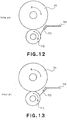
- Developing apparatuses provided with conventional developing blades as schematically shown in, e.g., Figures 9 to 13 .
- a blade 113 which has a thickness of 2 - 4 mm and is formed of a relatively high hardness resin or metal is mounted movably in a blade guide 114 through a coil spring 115.
- the blade 113 is pressed against a developing roller 112 rotating in a direction of an arrow B under a certain pressure.
- the developing roller 112 is rotatable in contact with an image bearing member (typically a photosensitive drum) 111 which is disposed opposite to the developing roller 112 and is rotated in a direction of an arrow A.
- a plate spring blade 113 formed in an L character shape at its one end portion is used.
- the other end portion of the blade 113 is fixed in a blade holder 114 formed of a high rigidity material, and the L character shaped edge (at one end portion) of the blade 113 is pressed against a developing roller 112 by its elastic force at a certain pressure.
- a blade 113 formed of an elastic material such as a rubber is extended and bonded to one end portion of a blade holder 114 and is pressed against a developing roller 112 at its end portion.
- a plate spring blade 113 formed in a U character shape at its one end portion is used.
- the other end portion of the blade 13 is fixed in a blade holder 114 formed of a high rigidity material and the U character shaped surface (at one end portion) of the blade 113 is pressed against a developing roller 112 by its elastic force at a certain pressure.
- a plate spring blade 113 is fixed in a blade holder 114 at its one end portion and is rounded at the other end portion through round-edge processing (not shown). The round-edged portion of the blade 113 is pressed against a developing roller 112 at a certain pressure.
- the developing blade shown in Figure 9 involves a problem of occurrences of a stripe due to a strain of the developing roller caused by generated creep and of "fog" caused by unevenness of a toner layer thickness.
- the developing blade shown in Figure 10 involves a problems of a deterioration of toner caused by small cracks at the L character shaped edge.
- the developing blade shown in Figure 11 involves a problem of a lowering in triboelectric chargeability caused by generated creep.
- the developing blade shown in Figure 12 involves a problem of sticking of toner caused by the limit of flatness.
- the developing blade shown in Figure 13 involves a problem of an irregularity in toner layer thickness caused by the limit of flatness and of an occurrence of "fog” caused by the irregularity in toner layer thickness.
- toner capable of being fixed at low temperature is desired with energy saving of equipments, so that, combined with color image formation, a thermal characteristic of toner is improved at low temperature.
- a developing apparatus which is generally effective in solving the above problem has been proposed in Japanese Laid-Open Patent Application JP 2001-147585 A .
- a toner layer thickness is regulated by causing a conformed edge of a metallic elastic blade to contact a developing roller.
- a charge amount per unit weight of the toner becomes large and a contact surface which regulates the toner is metal, so that the toner is liable to be fixedly deposited on the contact surface by image force. For this reason, with continuous printing, the toner is stuck on the contact surface to result in an occurrence of white stripe. Accordingly, the above described problem cannot be solved.
- EP 1 146 399 A discloses an image forming apparatus having a latent image carrier on which a latent image is formed.
- a developer carrier conveys a one-component non-magnetic developer and develops the latent image either in close proximity to or in contact with the latent image carrier.
- a voltage application unit applies an AC-superimposed bias voltage to the developer carrier.
- a regulating member abuts against the developer carrier to regulate the thickness of the developer layer on the developer carrier.
- the regulating member has a semiconductive member provided at the distal end thereof to produce an electric potential difference between the semiconductive member and the developer carrier, to which the AC-superimposed bias voltage is applied, when regulating the thickness of the developer layer on the developer carrier, thereby forming a line-shaped uneven conveying surface.
- JP 2002 207355 A discloses a developing device in which a blade is formed by laminating insulating layers on a conductive layer, and is attached to a casing so that the insulating comes into contact with a developing roller on the edge or on the side.
- a blade voltage for forming an alternating electric field superposed with a DC component on the contact part between the insulating layer and the developing roller is applied to the above conductive layer by a blade bias power source.
- JP 60 051857 A discloses a developing device in which an electric power source applies a voltage to an elastic body blade. By the voltage application, a developer layer is formed on a roller and stuck to a photosensitive body to perform development.
- JP 2000 112230 A discloses a developing device in which a rubber elastic body having a semi-circular convex face is fixed to a spring metal thin plate. An elastic coating layer is provided on the surface of the rubber elastic body. The rubber elastic body is fixed with the metal thin plate by chemical adhesion with an adhesive or by physical adhesion by biting on the metal thin plate.
- JP H11 174827 A discloses a developer regulation member comprising a flat spring as a regulation member.
- the regulation member comprises an elastic layer.
- a developer carrier has an elastic layer. An amount of developer on the developer carrier is restricted by the regulation member pressed on the developer carrier so that the regulation member can be in contact with the developing roller.
- An object of the present invention is to solve the above described problems in the conventional developing apparatuses, and to provide a developer regulation member, a developing apparatus and a process cartridge which are capable of performing either one or both of a layer thickness regulation function and a triboelectric charge function, and prevent an occurrence of fog image and sticking of developer.
- Another aim of the present invention is to provide a developer regulation member and a developing apparatus which does not cause an occurrence of stripe image even in a deformed state of a developing carrying member.
- Another aim of the present invention is to provide a developer regulation member and a developing apparatus which can be used in combination with toner having a small particle size and an improved thermal characteristic at low temperature and thus provide a simple apparatus structure, a high image quality, and a high reliability.
- a developing apparatus is stated in claim 7.
- a process cartridge is stated in claim 13.
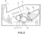
- Figure 2 is a schematic sectional view of an image forming apparatus 20 in which the developing apparatus of the present invention is mounted
- Figure 3 is a schematic sectional view of the developing apparatus of the present invention.
- a photosensitive drum 21 as an image bearing member is rotated in a direction of an arrow A, and is electrically charged uniformly by a charging apparatus 22. Thereafter, the surface of the photosensitive drum 21 is exposed to laser light 23 emitted from a laser optical apparatus to form an electrostatic latent image thereon.
- the electrostatic latent image is developed with toner by a developing apparatus 24 which is pressed in contact with the photosensitive drum 21 in a predetermined entering amount, thus being visualized as a toner image.
- the visualized toner image on the photosensitive drum 21 is transferred onto a recording medium 26 as a transfer(-receiving) material. Transfer residual toner remaining on the photosensitive drum 21 without being transferred is scraped with a cleaning blade 27 as a cleaning member and recovered in a waste toner container 28.
- the cleaned photosensitive drum 21 is repetitively subjected to the above described image forming process (cycle) to effect image formation.
- the recording medium 26 onto which the toner image is transferred is, after being subjected to permanent fixation of toner image by a fixing apparatus 29, discharged out of the image forming apparatus.
- the photosensitive drum and the developing apparatus are integrally disposed in a process cartridge detachably mountable to a main assembly of the image forming apparatus.
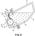
- the developing apparatus 24 is further described based on Figure 3 .
- a developer container 31 containing, as developer, negatively chargeable nonmagnetic monocomponent toner 32 is disposed.
- the developing apparatus 24 includes a developing roller 33 which is located at an opening extending in a longitudinal direction of the developer container 31 and is disposed opposite to the photosensitive drum 21.
- the developing roller 33 develops the electrostatic latent image on the photosensitive drum 21 which the toner to be visualized.
- the photosensitive drum 21 is a rigid body which comprises an aluminum cylinder as a support and a photosensitive layer coated in a predetermined thickness around the peripheral surface of the aluminum cylinder.
- the developing roller 33 having an elasticity has almost right half thereof located within the developer container 31 and almost left half thereof being exposed from the developer container 31. A part of the exposed surface of the developing roller 33 is disposed in contact with and opposite to the photosensitive drum 21 so as to be pressed against the photosensitive drum 21 in a predetermined entering amount. In this embodiment, the surface of the developing roller 33 contacts and enters the surface of the photosensitive drum 21 in an entering amount of 50 ⁇ m. In such a contact developing scheme that the developing roller is caused to contact the photosensitive drum, the developing roller may preferably possess elasticity.
- the developing roller 33 is rotated in a direction of an arrow B and the surface of which has an appropriate unevenness so as to improve a friction probability and permit a good conveyance performance of toner 32.
- the developing roller 33 in this embodiment has a two-layer structure comprising a silicone rubber support layer and a surface coating layer of acrylic-urethane rubber.
- the surface coating layer has a center-line average roughness Ra of 0.6 - 1.3 ⁇ m, and the developing roller 33 has an ASKER-C hardness of 45 - 65 degrees, a microrubber hardness of 35 - 55 degrees as measured by a microrubber hardness meter ("MD-1", mfd. by Kobunshi Keiki K.K.), and an electric resistance of 10 4 - 10 6 ohm.
- the electric resistance is measured in the following manner.
- the developing roller 33 is caused to contact an aluminum sleeve having the same diameter as the photosensitive drum 21 at a contact load of 500 gf (4.9 N).
- the aluminum sleeve is rotated at the same peripheral speed as the photosensitive drum 21.
- the photosensitive drum 21 has a diameter of 30 mm and is rotated at a peripheral speed of 900 mm/sec
- the developing roller 33 has a diameter of 20 mm and is rotated at a peripheral speed of 120 mm/sec higher than that of the photosensitive drum 21.
- a DC voltage of -300 V equal to the ordinary developing bias voltage in this embodiment is applied.
- a 100,000-ohm resistance is provided on a ground side and a voltage between both ends of the developing roller 33 is measured to determine an electric resistance of the developing roller 33.
- an elastic roller 34 for supplying toner to the developing roller 33 and scraping yet developed toner is caused to contact the developing roller 33 and is rotatably supported.
- the elastic roller 34 may preferably have a sponge structure or a fur brush structure wherein fibers, such as rayon and nylon, are planted on a core metal, from the viewpoints of toner supply and yet developed toner scraping.
- an urethane-based sponge roller is used and rotationally driven in the same direction as the developing roller 33.
- the core metal as a rotational shaft of the elastic roller 34 has a potential equal to that of the developing roller 33. Accordingly, when the electrostatic latent image on the photosensitive drum 21 is developed, the same voltage as the developing bias voltage is applied to the elastic roller 34.
- substantially spherical toner is used in order to provide a small particle size and improved transfer efficiency thereby to realize high image quality. More specifically, the spherical toner has a shape factor SF-1 of 100 - 180 and a shape factor SF-2 of 100 - 140.
- shape factors SF-1 and SF-2 are determined in the following manner.
- SF-1 and SF-2 are defined as values according to the following equations, respectively.
- SF ⁇ 1 MXLNG 2 / AREA ⁇ ⁇ / 4 ⁇ 100
- SF ⁇ 2 PERI 2 / AREA ⁇ ⁇ / 4 ⁇ 100
- MXLNG represents an absolute maximum length
- AREA represents a projection area of toner
- PERI represents a peripheral length.
- the shape factor SF-1 represents a sphericity, and as it is larger than 100, toner is gradually changed from spherical shape to indefinite shape.
- the shape factor SF-2 represents a degree of unevenness, and as it is larger than 100, a surface unevenness of toner becomes conspicuous.
- the toner may be produced through any production process so long as the shape factors thereof are in the above described ranges.
- a surface of a conventional toner produced through pulverization can be subjected to plastic spherical treatment under thermal/mechanical stress.
- a direct toner production process through suspension polymerization or dispersion polymerization using an aqueous organic solvent in which a monomer is soluble but a resultant polymer is insoluble.
- an emulsion polymerization, represented by soap-free polymerization wherein toner is produced through direct polymerization in the presence of an aqueous polar polymerization initiator.
- the resultant toner has a sharp particle distribution and a particle size of 4 - 8 ⁇ m.
- negatively chargeable toner having a weight-average particle size of about 7 ⁇ m and containing not more than 25 particle % of toner particles having a weight-average particle size of not more than 4 ⁇ m is produced through a suspension polymerization using styrene and n-butyl acrylate as a monomer, salicylic acid metal compound as a charge control agent, saturated polyester as a polar resin, and a colorant.
- the toner may preferably have a weight-average particle size of not more than 10 ⁇ m, more preferably not more than 7 ⁇ m.
- Measurement of the weight-average particle size of the toner is performed by a measuring apparatus ("Coulter Counter TA-II” or “Coulter Multisizer", mfd. by Coulter Co.).
- a 1 %-NaCl aqueous solution is prepared by using a reagent of first grade sodium chloride.
- 0.1 - 5 ml of a surfactant, preferably alkylbenzensulfonic acid is added as a dispersing agent, and 2 - 20 mg of a sample toner is further added.
- the resultant suspension electrolytic liquid is dispersed in an ultrasonic dispersion device for about 1 - 3 min.
- a volume and the number of particles of not less than 2 ⁇ m of the sample toner is measured by the measuring apparatus with a 100 pm-aperture, whereby a volume distribution and a number distribution are obtained. From the volume distribution, a weight-average particle size D4 is obtained.
- hydrophobic silica is externally added to the negatively chargeable toner.
- the addition amount of hydrophobic silica may appropriately be changed.
- a developing blade 35 as the developer regulation member having elasticity is supported by a supporting metal plate 38 and disposed in contact with the outer peripheral surface of the developing roller 33 at its free edge, in order to regulate an amount of developer carried on the developing roller 33.
- the contact direction of the developing blade 35 is such that the free edge contacting the developing roller 33 is located upstream from a position extended from a supporting portion of the developing blade 35 in the rotation direction of the developing roller 33.
- the developing blade 35 may be supported on the supporting metal plate 38 by fastening with a screw, welding, etc. Further, the developing blade 35 and the supporting metal plate 38 have the same potential as the developing roller 33, so that the same voltage as the developing bias voltage is applied thereto when the electrostatic latent image on the photosensitive drum 21 is developed.
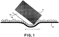
- the developing blade 35 comprises, as a first regulation portion, a thin metal plate 11 of phosphor bronze and, as a second regulation portion, an elastic layer of polyamide-containing rubber (polyamide elastomer) 12.
- polyamide elastomer polyamide-containing rubber
- the thin metal plate 11 as the first regulation portion is disposed upstream of the polyamide elastomer layer 12 as the second regulation portion in the conveyance direction of developer carried on the developing roller 33.
- the second regulation portion is disposed at the opposing surface, of the developing blade, where the developing roller and the developing blade are opposed to each other.
- the developer regulation member comprises the first and second regulation portions which is different in mater as described above and regulate the amount of developer carried on the developing roller 33 by pressing it against the developing roller 33.
- the regulation portion includes the first regulation portion formed of a material having a Shore D hardness of not less than 70 degrees or metal, and its free edge disposed in contact with the developing roller, so that it is possible to uniformly regulate the thickness of layer of developer even when the surface of the developing roller is deformed.
- the developing blade contacts the developing roller but the free edge of the developing blade is not in contact with the developing roller, an unevenness in layer thickness of developer is caused to occur when the developing roller has been deformed, thus resulting in an irregularity in development.
- the second regulation portion is disposed in contact with the developing roller but in addition to the second regulation portion, the thin metal plate as the first regulation portion may also be disposed in contact with the developing roller.
- the thin metal plate 11 may preferably be formed of metal, such as SUS stainless steel or a material having a Shore D hardness of not less than 70 degrees, such as polypropylene, ABS (acrylonitrile material may be electroconductive or nonelectro-conductive.
- the elastic layer 12 may also be formed of a material having an electric resistance higher than metal, preferably not less than 10 6 ohm.cm (as measured according to IEC 93 under an environment of 23 °C/50 %RH), more preferably not less than 10 8 ohm.cm.
- the electric layer 12 may have a hardness such that it is softer than metal, and may preferably be those having a Shore D hardness of not more than 70 degrees (e.g., polypropylene, nylon, polyester elastomer, etc.), more preferably be those having a Shore D hardness of not more than 40 degrees (e.g. TPU (thermoplastic polyurethane) etc.).
- a Shore D hardness of not more than 70 degrees (e.g., polypropylene, nylon, polyester elastomer, etc.), more preferably be those having a Shore D hardness of not more than 40 degrees (e.g. TPU (thermoplastic polyurethane) etc.).
- the polyamide elastomer comprises polyamide and polyester which are linked with an ester linkage or an amide linkage.
- the anode component is not particularly limited but may generally be selected from the group consisting of 6-nylon; 6,6-nylon; 6,12-nylon; 11-nylon; 12-nylon; 12,12-nylon; and copolyamides obtained through polycondensation of monomers of these nylons.
- dibasic acid may include: aliphatic saturated dicarboxylic acids, such as oxalic acid, succinic acid, adipic acid, suberic acid, sebacic acid, and dodecanedioic acid; aliphatic unsaturated dicarboxylic acids such as maleic acid; aromatic dicarboxylic acids, such as phthalic acid, and terephthalic acid; and polydicarboxylic acids comprising the above described dibasic acids and diols, such as ethylene glycol, butanediol, hexanediol and octanediol.
- polyether component it is possible to use polyethers, such as polyethylene glycol, polypropylene glycol, and polytetramethylene glycol; and polyether diamine having an aminated terminal group.
- the polyamide elastomer used in this embodiment comprises 12-nylon as the polyamide component, dodecanedioic acid as the dibasic acid, and polytetramethylene glycol as the polyether component. These components are reacted and dried for predetermined hours, followed by lamination on the phosphor bronze thin metal plate.
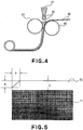
- the developing blade may be prepared through, e.g., a roll coating method shown in Figure 4 .
- a surface transfer sheet 44 is mounted on a roller 42, and a starting material 45 for the blade member is fed from a nozzle 41 through a predetermined spacing between the roller 42 and a roller 43 and then is solidified.
- a blade member having a charge control surface coated with the surface transfer sheet is obtained.
- films of polyester resin, polyamide resin, polyolefin resin, a copolymer of these resins, and an alloy of these resins may be used.
- films of at least one species of the material selected from the group consisting of polyethylene terephthalate, polyethylene-2,6-naphthalate, a copolymer of these, and a composite of these may preferably be used.
- the above prepared blade member having the charge control surface coated with the surface transfer sheet is cut from the surface transfer sheet side so that its end portion has a predetermined shape (an inclined portion) by using a method, such as punching.
- the blade member has an edge portion, for regulating developer, which has a shape as shown in Figure 5 . This shape is provided by polishing but may also be provided by another method, such as molding.
- the developing blade used in the present invention may preferably be prepared so as to satisfy the following relationship: ⁇ 20 ⁇ t ⁇ a ⁇ 25, and t ⁇ b ⁇ 25, wherein t represents a thickness ( ⁇ m) of the elastic layer 12 laminated on the thin metal plate 11, a represents a length ( ⁇ m) of the inclined portion of the blade in the lamination direction, and b represents a length ( ⁇ m) of the inclined portion of the blade in a direction perpendicular to the lamination direction.
- the developing blade 35 in this embodiment is disposed in contact (abutment) with the developing roller 33 at a contact (abutment) pressure of 20 - 40 g/cm.
- a nip (width) between the developing roller 33 and the developing blade 35 i.e., a distance from the developing blade edge to a portion at which the developing roller 33 and the developing blade 35 are in a noncontact state
- the thin metal plate 11 of phosphor bronze has a thickness of 120 ⁇ m
- the elastic layer 12 of polyamide elastomer has a thickness of 30 ⁇ m.
- a print out test on 1000 sheets was performed by using the above described image forming apparatus 20 and the developing apparatus 24 in environments normal temperature/normal humidity (NT/NH) (25 °C/60 %RH), low temperature/low humidity (LT/LH) (15 °C/10 %RH), and high temperature/high humidity (HT/HH) (30 °C/80 %RH).
- NT/NH normal temperature/normal humidity
- LH low temperature/low humidity
- HT/HH high temperature/high humidity
- the sticking was attributable to an electric charge of the toner as the developer, and an electrical factor, and that the toner having a large electric charge was liable to be deposited on the metal surface by image force.
- the printout (image formation) test on 2000 sheets was performed in the LT/LH (15 °C/10 %RH) environment by changing an electric resistance of the toner regulation portion , and a degree of occurrence of sticking matter on three developing blades A, B and C described below was observed for evaluation.
- the developing apparatus the conventional developing apparatus was used.
- the conventional elastic blade 61 comprising a 0.12 mm-thick metal plate formed of phosphor bronze shown in Figure 6 was used.
- a developing blade comprising the conventional developing blade A (0.12 mm-thick phosphor bronze made thin metal plate) and a 0.5 mm thick resistance layer which was controlled to have a volume resistivity of 10 3 ohm.cm by dispersing carbon black particles (as an electroconductive agent) in phenolic resin and was dip-coated on the thin metal plate so as to cover an entire portion from one end of the thin metal plate to the other end (to be in contact with the developing roller) thereof.
- a developing blade comprising the conventional developing blade A (0.12 mm-thick phosphor bronze-made thin metal plate) and a 0.5 mm-thick resistance layer which was controlled to have a volume resistivity of 10 6 ohm.cm by dispersing carbon black particles (as an electroconductive agent) in phenolic resin and was dip-coated on the thin metal plate so as to cover an entire portion from one end of the thin metal plate to the other end (to be in contact with the developing roller) thereof.
- two developing blades D and E were prepared by using a material which had a high electric resistance and a good triboelectric chargeability with respect to the negatively chargeable toner, and were subjected to a durability test of the developing blades through the printout (image formation) test.
- an elastic developing blade D having a volume resistivity of 10 8 ohm.cm was prepared by using a material comprising polyamide elastomer 12 which contained a polyamide component and an elastic polyether component. More specifically, a lamination structure comprising a 0.12 mm-thick phosphor bronze metal plate 11 (first regulation portion) and a 30 pm-thick polyamide elastomer layer 12 (second regulation portion) was prepared by using the roll coating method described in the above described embodiment and then formed through punching.
- an elastic developing blade E having a volume resistivity of 10 9 ohm.cm was prepared by using a material comprising polypropylene. More specifically, on a 0.12 mm-thick phosphor bronze metal plate 81 having a spring characteristic, a 0.2 mm-thick polypropylene film 12 having a width of 5 mm was fixed with an adhesive. In this embodiment, the developing regulation portion was consisting only of the polypropylene film 12.
- the developing blade D had a Share D hardness of 40 degrees and the developing blade E had a Shore D hardness of 70 degrees, so that the developing blade E imposed a larger stress on the regulation portion of the developing blade E to cause the white stripe.
- the second regulation portion may preferably have a Shore D hardness of less than 70 degrees.
- the volume resistivity of the second regulation portion located on the downstream side may desirably be larger than that of the first regulation portion, more desirably be not less than 10 6 ohm.cm.
- the developing blade D As described above, by using the developing blade D, the toner sticking onto the developing blade was not caused to occur. Further, the developing blade per se had a high triboelectric chargeability, thus effectively imparting triboelectric charge to the quality image with no fog image.
- the hardness of the toner layer thickness regulation portion was preferably not less than 70 degrees in terms of Shore D hardness or the toner layer thickness regulation portion was formed of metal. This may be attributable to such a phenomenon that the toner layer thickness regulation portion having a larger hardness is liable to permit the developing blade which can readily follow the deformed portion of the developing roller, thus being capable of providing a uniform layer thickness of developer. Further, as already described above, the abutment (contact) of the free edge of the developing blade against the developing roller was effective in suppressing the occurrence of the stripe image. This also may be attributable to the edge abutment, of the developing blade against the developing roller, permitting the developing blade which is more liable to follow the deformed portion of the developing roller.
- the hardness of the first regulation portion of the developing blade located on the upstream side (where the developing blade does not face the developing roller) in the conveyance direction of developer by the developing roller may desirably be higher than that of the second regulation portion (facing the developing roller).
- developing blade F developing blade F
- the polyamide elastomer layer 12 (second regulation portion) of the developing blade D was abraded or beveled to provide the developing blade D with an inclined edge portion in a contact portion of the developing blade D with the developing roller 13.
- the second regulation portion 12 has an obtuse edge at its end portion.
- the developing blade having the lamination structure of the metal layer and the polyamide elastomer layer is used but the structure of the developing blade may be appropriately modified so long as it can regulate the toner layer in the order of the metal layer and the polyamide elastomer layer from the upstream side in the developer conveyance direction at the toner regulation portion by, e.g., embedding metal in the polyamide elastomer layer.
- the developing blade F By using the developing blade F, toner sticking onto the developing blade F is not caused to occur, and the developing blade F per se has a high triboelectric chargeability, thus effectively imparting triboelectric charge to the toner. Accordingly, it was possible to obtain a high quality image with no fog image and no occurrence of stripe image even in such a circumstance that the developing roller caused creep deformation.
- the developer regulation member is constituted by two regulation portions but may be constituted by three or more regulation portions which are laminated together.
- the inclined portion as described above may preferably be formed in two or more regulation portions other than the most upstream regulation portion in the developer conveyance direction.
- toner sticking onto the developer regulation member is not cause to occur, and the developer regulation member per se has a high triboelectric chargeability, thus effectively imparting triboelectric charge to the toner. Accordingly, it was possible to obtain a high quality image with no fog image and no occurrence of stripe image even in such a circumstance that the developing roller caused creep deformation.
Landscapes
- Physics & Mathematics (AREA)
- General Physics & Mathematics (AREA)
- Dry Development In Electrophotography (AREA)
- Developing Agents For Electrophotography (AREA)
Claims (14)
- Entwicklerregulierelement mit:einer Entwicklerreguliereinrichtung (35) zum Regulieren einer Menge eines Entwicklers, der auf einem Entwicklertrageelement (33) befördert wird, das einen Kernmetallabschnitt hat, wobei die Entwicklerreguliereinrichtung (35) eine laminierte Struktur aufweist, die einen ersten Regulierabschnitt (11), der aus einem ersten Material ausgebildet ist, das eine Härte nach Shore D von nicht weniger als 70 Grad hat oder Metall ist, und einen zweiten Regulierabschnitt (12) hat, der an einer Seite in der Nähe des Entwicklertrageelementes (33) anordenbar ist und der aus einem Material ausgebildet ist, das sich von dem ersten Material für den ersten Regulierabschnitt (11) unterscheidet, wobei die Härte des ersten Regulierabschnittes (11) höher ist als jene des zweiten Regulierabschnittes (12), undeiner Stützmetallplatte (38) zum Abstützen der Entwicklerreguliereinrichtung (35),wobei die Entwicklerreguliereinrichtung (35) einen Rand hat, der mit dem Entwicklertrageelement (33) in Kontakt bringbar ist,wobei der Rand einen geneigten Abschnitt in einer vorbestimmten Form an dem zweiten Regulierabschnitt (12) hat und die folgenden Beziehungen erfüllt:
 dadurch gekennzeichnet, dassin der Anwendung eine an dem Kernmetallabschnitt der Entwicklerreguliereinrichtung (35) angelegte Vorspannung die gleiche wie eine Spannung ist, die an der Stützmetallplatte (38) angelegt ist, wenn das elektrostatische latente Bild entwickelt wird.
 - Entwicklerregulierelement gemäß Anspruch 1, wobei der zweite Regulierabschnitt (12) eine Härte hat, die niedriger ist als bei dem ersten Regulierabschnitt (11).
- Entwicklerregulierelement gemäß Anspruch 1, wobei der zweite Regulierabschnitt (12) einen spezifischen Durchgangswiderstand hat, der höher ist als bei dem ersten Regulierabschnitt (11).
- Entwicklerregulierelement gemäß Anspruch 1, wobei der erste Regulierabschnitt (11) stromaufwärtig von dem zweiten Regulierabschnitt (12) in einer Beförderungsrichtung des Entwicklers angeordnet ist, der auf dem Entwicklertrageelement (23) getragen wird, wobei der zweite Regulierabschnitt einen spezifischen Durchgangswiderstand von nicht weniger als 106 ohm.cm hat.
- Entwicklerregulierelement gemäß Anspruch 1, wobei die Entwicklerreguliereinrichtung (35) einen Regulierabschnitt aufweist, der am weitesten stromabwärtig in einer Beförderungsrichtung des Entwicklers, der auf dem Entwicklertrageelement (33) getragen wird, angeordnet ist und einen spezifischen Durchgangswiderstand von nicht weniger als 106 ohm.cm hat.
- Entwicklerregulierelement gemäß Anspruch 1, wobei der zweite Regulierabschnitt (12) einen stumpfen Endabschnitt hat.
- Entwicklungsvorrichtung (24) mit:einem Entwicklertrageelement (33) mit einer Elastizität zum Entwickeln eines elektrostatischen latenten Bildes, das auf einem Bildtrageelement (21) erzeugt wird, mit einem Entwickler, undeinem Entwicklerregulierelement gemäß einem der Ansprüche 1 bis 6.
- Vorrichtung gemäß Anspruch 7, wobei das Entwicklertrageelement (33) ein elastisches Entwicklertrageelement ist.
- Vorrichtung gemäß Anspruch 7 oder 8, die für einen Entwickler anwendbar ist, der eine durchschnittliche Volumenpartikelgröße von nicht mehr als 10 µm hat.
- Vorrichtung gemäß Anspruch 7 oder 8, die für einen Entwickler anwendbar ist, der eine durchschnittliche Volumenpartikelgröße von nicht mehr als 7 µm hat.
- Vorrichtung gemäß Anspruch 7 oder 8, die für einen Entwickler anwendbar ist, der ein nichtmagnetischer Monokomponentenentwickler ist.
- Vorrichtung gemäß Anspruch 7 oder 8, wobei das Entwicklertrageelement (33) mit dem Entwicklertrageelement (21) in Kontakt bringbar angeordnet ist.
- Prozesskartusche, die an einer Hauptbaugruppe einer Bilderzeugungsvorrichtung ablösbar montiert ist, mit:der Entwicklungsvorrichtung (24) gemäß einem der Ansprüche 7 bis 12, undeinem Bildtrageelement (21),wobei die Entwicklungsvorrichtung (24) und das Bildtrageelement (21) in der Prozesskartusche einstückig angeordnet sind.
- Entwicklerregulierelement gemäß Anspruch 1, wobei der zweite Regulierabschnitt (12) auf einer gesamten Oberfläche des ersten Regulierabschnittes (11) von einem Ende an einer Seite, an der die Entwicklerreguliereinrichtung (35) durch ein Stützelement (38) abgestützt ist, bis zu einem freien Ende, das nahe einer Außenumfangsfläche des Entwicklertrageelementes (33) ist, laminiert ist.
Applications Claiming Priority (2)
| Application Number | Priority Date | Filing Date | Title |
|---|---|---|---|
| JP2003276048A JP4402391B2 (ja) | 2003-07-17 | 2003-07-17 | 現像装置 |
| JP2003276048 | 2003-07-17 |
Publications (3)
| Publication Number | Publication Date |
|---|---|
| EP1507175A2 EP1507175A2 (de) | 2005-02-16 |
| EP1507175A3 EP1507175A3 (de) | 2005-02-23 |
| EP1507175B1 true EP1507175B1 (de) | 2018-09-12 |
Family
ID=33562740
Family Applications (1)
| Application Number | Title | Priority Date | Filing Date |
|---|---|---|---|
| EP04016694.4A Expired - Lifetime EP1507175B1 (de) | 2003-07-17 | 2004-07-15 | Entwicklungsregelungsteil und Entwicklungsgerät |
Country Status (5)
| Country | Link |
|---|---|
| US (1) | US7239832B2 (de) |
| EP (1) | EP1507175B1 (de) |
| JP (1) | JP4402391B2 (de) |
| KR (1) | KR100678542B1 (de) |
| CN (1) | CN100504638C (de) |
Families Citing this family (9)
| Publication number | Priority date | Publication date | Assignee | Title |
|---|---|---|---|---|
| JP2007021482A (ja) * | 2005-06-14 | 2007-02-01 | Sumiko Eco-Engineering Co Ltd | アンモニア分解触媒及びアンモニア処理方法 |
| JP2007148388A (ja) * | 2005-11-01 | 2007-06-14 | Canon Inc | 画像形成装置 |
| JP5277662B2 (ja) | 2008-03-03 | 2013-08-28 | 株式会社リコー | プロセスカートリッジ、これを備えた現像装置、画像形成装置 |
| JP2010008994A (ja) * | 2008-05-27 | 2010-01-14 | Canon Inc | トナー供給ローラ、現像装置および画像形成装置 |
| CN102309809B (zh) * | 2010-07-09 | 2013-11-20 | 同济大学 | 造口术系统 |
| JP6157276B2 (ja) | 2013-08-23 | 2017-07-05 | キヤノン株式会社 | 現像装置、プロセスカートリッジ、画像形成装置 |
| JP2015041084A (ja) | 2013-08-23 | 2015-03-02 | キヤノン株式会社 | 現像装置、プロセスカートリッジ、画像形成装置 |
| JP2015069166A (ja) * | 2013-09-30 | 2015-04-13 | ブラザー工業株式会社 | 現像装置、ブレードユニット、および、現像装置の製造方法 |
| JP7592451B2 (ja) | 2020-10-14 | 2024-12-02 | キヤノン株式会社 | 現像装置、プロセスカートリッジおよび画像形成装置 |
Citations (3)
| Publication number | Priority date | Publication date | Assignee | Title |
|---|---|---|---|---|
| JPH04355777A (ja) * | 1991-06-03 | 1992-12-09 | Matsushita Electric Ind Co Ltd | 乾式現像装置のトナー薄層化ブレード |
| JPH11174827A (ja) * | 1997-12-09 | 1999-07-02 | Minolta Co Ltd | 現像装置 |
| EP1146399A2 (de) * | 2000-04-10 | 2001-10-17 | Seiko Epson Corporation | Bilderzeugungsgerät |
Family Cites Families (24)
| Publication number | Priority date | Publication date | Assignee | Title |
|---|---|---|---|---|
| JPS57165866A (en) * | 1981-04-07 | 1982-10-13 | Toshiba Corp | Developing device |
| JPS6051857A (ja) | 1983-08-31 | 1985-03-23 | Toshiba Corp | 現像装置 |
| JPS61223769A (ja) * | 1985-03-28 | 1986-10-04 | Fuji Xerox Co Ltd | 一成分現像装置 |
| JP3435642B2 (ja) | 1992-12-22 | 2003-08-11 | 株式会社リコー | 現像装置 |
| JP3106028B2 (ja) | 1993-03-09 | 2000-11-06 | キヤノン株式会社 | 現像剤量規制部材及びその製造方法そしてこの部材を備える現像装置 |
| JPH06348119A (ja) * | 1993-06-10 | 1994-12-22 | Canon Inc | 現像装置 |
| JPH07219339A (ja) | 1994-01-31 | 1995-08-18 | Canon Inc | 弾性ブレード及びその製造方法及び現像装置 |
| JP3275226B2 (ja) * | 1995-05-31 | 2002-04-15 | キヤノン株式会社 | 現像剤量規制部材及び現像装置 |
| JP3048222B2 (ja) * | 1996-05-27 | 2000-06-05 | キヤノン株式会社 | 現像剤規制部材及び現像装置 |
| JP3443519B2 (ja) * | 1996-09-30 | 2003-09-02 | 京セラ株式会社 | ブレード |
| JPH10307472A (ja) * | 1997-05-08 | 1998-11-17 | Minolta Co Ltd | 現像装置 |
| JP3445126B2 (ja) | 1997-11-17 | 2003-09-08 | キヤノン株式会社 | 画像形成方法及び画像形成装置 |
| JP2000112230A (ja) | 1998-10-05 | 2000-04-21 | Polymatech Co Ltd | 電子写真装置用現像ブレードおよびその製造方法 |
| DE60016299T2 (de) * | 1999-03-11 | 2005-11-10 | Brother Kogyo K.K., Nagoya | Entwicklungsgerät mit Regulierteil für die Entwicklerschichtdicke, Kassette und Bilderzeugungsapparat mit einem solchen Gerät |
| JP2001022176A (ja) * | 1999-07-13 | 2001-01-26 | Canon Inc | 現像装置及びこの現像装置を備えるプロセスカートリッジ並びに画像形成装置 |
| JP2001042641A (ja) * | 1999-08-04 | 2001-02-16 | Fujitsu Ltd | 現像剤、現像方法、現像装置及びその構成要素、並びに、画像形成装置 |
| US6360068B1 (en) * | 1999-11-19 | 2002-03-19 | Fujitsu Limited | Electrophotographic image formation process and apparatus |
| JP2001147585A (ja) | 1999-11-19 | 2001-05-29 | Fujitsu Ltd | 画像形成方法及び装置 |
| JP3519044B2 (ja) | 1999-12-28 | 2004-04-12 | シャープ株式会社 | 現像装置 |
| JP2001242709A (ja) * | 2000-03-01 | 2001-09-07 | Canon Inc | 現像装置、カートリッジおよび電子写真画像形成装置 |
| JP4659233B2 (ja) * | 2001-02-27 | 2011-03-30 | キヤノン株式会社 | 現像剤規制部材、現像装置、プロセスカートリッジ及び画像形成装置 |
| JP2002372855A (ja) | 2001-04-13 | 2002-12-26 | Canon Chemicals Inc | 現像剤量規制ブレード、現像装置、現像剤量規制ブレードの製造方法 |
| JP3997065B2 (ja) * | 2001-08-20 | 2007-10-24 | キヤノン株式会社 | プロセスカートリッジ及び画像形成装置 |
| JP2004012542A (ja) * | 2002-06-03 | 2004-01-15 | Canon Inc | 現像剤規制部材、現像装置、プロセスカートリッジ及び画像形成装置 |
-
2003
- 2003-07-17 JP JP2003276048A patent/JP4402391B2/ja not_active Expired - Fee Related
-
2004
- 2004-07-14 US US10/890,147 patent/US7239832B2/en not_active Expired - Lifetime
- 2004-07-15 EP EP04016694.4A patent/EP1507175B1/de not_active Expired - Lifetime
- 2004-07-16 KR KR1020040055414A patent/KR100678542B1/ko not_active Expired - Fee Related
- 2004-07-19 CN CNB2004100697765A patent/CN100504638C/zh not_active Expired - Fee Related
Patent Citations (3)
| Publication number | Priority date | Publication date | Assignee | Title |
|---|---|---|---|---|
| JPH04355777A (ja) * | 1991-06-03 | 1992-12-09 | Matsushita Electric Ind Co Ltd | 乾式現像装置のトナー薄層化ブレード |
| JPH11174827A (ja) * | 1997-12-09 | 1999-07-02 | Minolta Co Ltd | 現像装置 |
| EP1146399A2 (de) * | 2000-04-10 | 2001-10-17 | Seiko Epson Corporation | Bilderzeugungsgerät |
Also Published As
| Publication number | Publication date |
|---|---|
| CN100504638C (zh) | 2009-06-24 |
| JP2005037775A (ja) | 2005-02-10 |
| JP4402391B2 (ja) | 2010-01-20 |
| EP1507175A3 (de) | 2005-02-23 |
| US7239832B2 (en) | 2007-07-03 |
| EP1507175A2 (de) | 2005-02-16 |
| US20050025531A1 (en) | 2005-02-03 |
| KR100678542B1 (ko) | 2007-02-07 |
| CN1577161A (zh) | 2005-02-09 |
| KR20050009220A (ko) | 2005-01-24 |
Similar Documents
| Publication | Publication Date | Title |
|---|---|---|
| JP3492273B2 (ja) | 現像装置 | |
| EP0747782B1 (de) | Elastische Schneide um Entwicklerzufuhr zu Steuern, und diese benutzendes Entwicklungsgerät | |
| US5311264A (en) | Developing apparatus for developing electrostatic latent image using one component developer | |
| US5565968A (en) | Developing roller, and method and apparatus for developing latent images using the roller | |
| EP0810488B1 (de) | Entwicklungsregelungsteil und Entwicklungsgerät | |
| US6952551B2 (en) | Developer carrying member and developing apparatus | |
| EP1507175B1 (de) | Entwicklungsregelungsteil und Entwicklungsgerät | |
| JPH03236074A (ja) | 現像装置 | |
| EP1237050B1 (de) | Entwicklungsregelungsteil und dieses Teil enthaltendes Entwicklungsgerät | |
| US20040223789A1 (en) | Developing apparatus | |
| EP0636950A2 (de) | Entwicklungsgerät mit einer sich drehenden Entwicklerzufuhreinheit einer Entwicklerträgereinheit | |
| US5666620A (en) | Developing device for peeling toner using peeling rotary member | |
| JP5365732B2 (ja) | 帯電装置、プロセスカートリッジ及び画像形成装置 | |
| JP3136288B2 (ja) | 現像装置 | |
| US20220107585A1 (en) | Image forming apparatus | |
| US20050141923A1 (en) | Image forming apparatus | |
| US6341204B1 (en) | Development apparatus employing toner supply roller comprising electrically conductive foamed material layer | |
| JP5145846B2 (ja) | 帯電装置、プロセスカートリッジ及び画像形成装置 | |
| US7505719B2 (en) | Composite trim bar for developer system | |
| JP7183029B2 (ja) | クリーニング装置、カートリッジ及び画像形成装置 | |
| JP2008233157A (ja) | 現像ローラ | |
| JP2001109259A (ja) | 現像剤規制部材、現像装置及びプロセスカートリッジ並びに画像形成装置 | |
| JP2930508B2 (ja) | 現像装置およびこの現像装置を備える画像形成装置 | |
| JP2024063306A (ja) | 画像形成装置 | |
| JP2006017812A (ja) | 現像ローラ、現像装置及び電子写真プロセスカートリッジ |
Legal Events
| Date | Code | Title | Description |
|---|---|---|---|
| PUAI | Public reference made under article 153(3) epc to a published international application that has entered the european phase |
Free format text: ORIGINAL CODE: 0009012 |
|
| PUAL | Search report despatched |
Free format text: ORIGINAL CODE: 0009013 |
|
| 17P | Request for examination filed |
Effective date: 20040715 |
|
| AK | Designated contracting states |
Kind code of ref document: A2 Designated state(s): AT BE BG CH CY CZ DE DK EE ES FI FR GB GR HU IE IT LI LU MC NL PL PT RO SE SI SK TR |
|
| AX | Request for extension of the european patent |
Extension state: AL HR LT LV MK |
|
| AK | Designated contracting states |
Kind code of ref document: A3 Designated state(s): AT BE BG CH CY CZ DE DK EE ES FI FR GB GR HU IE IT LI LU MC NL PL PT RO SE SI SK TR |
|
| AX | Request for extension of the european patent |
Extension state: AL HR LT LV MK |
|
| AKX | Designation fees paid |
Designated state(s): DE FR GB |
|
| 17Q | First examination report despatched |
Effective date: 20071129 |
|
| GRAP | Despatch of communication of intention to grant a patent |
Free format text: ORIGINAL CODE: EPIDOSNIGR1 |
|
| RIN1 | Information on inventor provided before grant (corrected) |
Inventor name: TAKASHIMA, KOICHIRO Inventor name: KOYANAGI, MASATO Inventor name: ISHII, YASUYUKI |
|
| INTG | Intention to grant announced |
Effective date: 20180326 |
|
| GRAS | Grant fee paid |
Free format text: ORIGINAL CODE: EPIDOSNIGR3 |
|
| GRAA | (expected) grant |
Free format text: ORIGINAL CODE: 0009210 |
|
| AK | Designated contracting states |
Kind code of ref document: B1 Designated state(s): DE FR GB |
|
| REG | Reference to a national code |
Ref country code: GB Ref legal event code: FG4D |
|
| REG | Reference to a national code |
Ref country code: DE Ref legal event code: R096 Ref document number: 602004053162 Country of ref document: DE |
|
| RIC2 | Information provided on ipc code assigned after grant |
Ipc: G03G 15/08 20060101AFI20041215BHEP |
|
| REG | Reference to a national code |
Ref country code: DE Ref legal event code: R097 Ref document number: 602004053162 Country of ref document: DE |
|
| PLBE | No opposition filed within time limit |
Free format text: ORIGINAL CODE: 0009261 |
|
| STAA | Information on the status of an ep patent application or granted ep patent |
Free format text: STATUS: NO OPPOSITION FILED WITHIN TIME LIMIT |
|
| 26N | No opposition filed |
Effective date: 20190613 |
|
| PGFP | Annual fee paid to national office [announced via postgrant information from national office to epo] |
Ref country code: FR Payment date: 20190725 Year of fee payment: 16 |
|
| PGFP | Annual fee paid to national office [announced via postgrant information from national office to epo] |
Ref country code: GB Payment date: 20190729 Year of fee payment: 16 |
|
| PGFP | Annual fee paid to national office [announced via postgrant information from national office to epo] |
Ref country code: DE Payment date: 20190930 Year of fee payment: 16 |
|
| REG | Reference to a national code |
Ref country code: DE Ref legal event code: R119 Ref document number: 602004053162 Country of ref document: DE |
|
| GBPC | Gb: european patent ceased through non-payment of renewal fee |
Effective date: 20200715 |
|
| PG25 | Lapsed in a contracting state [announced via postgrant information from national office to epo] |
Ref country code: GB Free format text: LAPSE BECAUSE OF NON-PAYMENT OF DUE FEES Effective date: 20200715 Ref country code: FR Free format text: LAPSE BECAUSE OF NON-PAYMENT OF DUE FEES Effective date: 20200731 |
|
| PG25 | Lapsed in a contracting state [announced via postgrant information from national office to epo] |
Ref country code: DE Free format text: LAPSE BECAUSE OF NON-PAYMENT OF DUE FEES Effective date: 20210202 |