EP1506557B1 - Chipkondensator und verfahren zu dessen herstellung - Google Patents
Chipkondensator und verfahren zu dessen herstellung Download PDFInfo
- Publication number
- EP1506557B1 EP1506557B1 EP03752708A EP03752708A EP1506557B1 EP 1506557 B1 EP1506557 B1 EP 1506557B1 EP 03752708 A EP03752708 A EP 03752708A EP 03752708 A EP03752708 A EP 03752708A EP 1506557 B1 EP1506557 B1 EP 1506557B1
- Authority
- EP
- European Patent Office
- Prior art keywords
- capacitor
- anode
- bodies
- contacts
- cathode contact
- Prior art date
- Legal status (The legal status is an assumption and is not a legal conclusion. Google has not performed a legal analysis and makes no representation as to the accuracy of the status listed.)
- Expired - Lifetime
Links
- 239000003990 capacitor Substances 0.000 title claims abstract description 159
- 238000004519 manufacturing process Methods 0.000 title claims description 16
- 238000000034 method Methods 0.000 title claims description 15
- 239000000853 adhesive Substances 0.000 claims description 10
- 230000001070 adhesive effect Effects 0.000 claims description 10
- 238000003466 welding Methods 0.000 claims description 7
- 239000000969 carrier Substances 0.000 claims description 6
- 229910052751 metal Inorganic materials 0.000 claims description 6
- 239000002184 metal Substances 0.000 claims description 6
- 230000000712 assembly Effects 0.000 claims description 2
- 238000000429 assembly Methods 0.000 claims description 2
- NUJOXMJBOLGQSY-UHFFFAOYSA-N manganese dioxide Chemical compound O=[Mn]=O NUJOXMJBOLGQSY-UHFFFAOYSA-N 0.000 description 4
- GUVRBAGPIYLISA-UHFFFAOYSA-N tantalum atom Chemical compound [Ta] GUVRBAGPIYLISA-UHFFFAOYSA-N 0.000 description 4
- BQCADISMDOOEFD-UHFFFAOYSA-N Silver Chemical compound [Ag] BQCADISMDOOEFD-UHFFFAOYSA-N 0.000 description 2
- 238000005452 bending Methods 0.000 description 2
- 238000000926 separation method Methods 0.000 description 2
- 229910052709 silver Inorganic materials 0.000 description 2
- 239000004332 silver Substances 0.000 description 2
- OKTJSMMVPCPJKN-UHFFFAOYSA-N Carbon Chemical compound [C] OKTJSMMVPCPJKN-UHFFFAOYSA-N 0.000 description 1
- 238000005520 cutting process Methods 0.000 description 1
- 230000001419 dependent effect Effects 0.000 description 1
- 229910002804 graphite Inorganic materials 0.000 description 1
- 239000010439 graphite Substances 0.000 description 1
- 238000003780 insertion Methods 0.000 description 1
- 230000037431 insertion Effects 0.000 description 1
- MIVBAHRSNUNMPP-UHFFFAOYSA-N manganese(2+);dinitrate Chemical compound [Mn+2].[O-][N+]([O-])=O.[O-][N+]([O-])=O MIVBAHRSNUNMPP-UHFFFAOYSA-N 0.000 description 1
- 229910052758 niobium Inorganic materials 0.000 description 1
- 239000010955 niobium Substances 0.000 description 1
- GUCVJGMIXFAOAE-UHFFFAOYSA-N niobium atom Chemical compound [Nb] GUCVJGMIXFAOAE-UHFFFAOYSA-N 0.000 description 1
- 230000003647 oxidation Effects 0.000 description 1
- 238000007254 oxidation reaction Methods 0.000 description 1
- 239000003973 paint Substances 0.000 description 1
- 229920000642 polymer Polymers 0.000 description 1
- 238000000197 pyrolysis Methods 0.000 description 1
- 229910052715 tantalum Inorganic materials 0.000 description 1
Images


Classifications
-
- H—ELECTRICITY
- H01—ELECTRIC ELEMENTS
- H01G—CAPACITORS; CAPACITORS, RECTIFIERS, DETECTORS, SWITCHING DEVICES, LIGHT-SENSITIVE OR TEMPERATURE-SENSITIVE DEVICES OF THE ELECTROLYTIC TYPE
- H01G4/00—Fixed capacitors; Processes of their manufacture
- H01G4/38—Multiple capacitors, i.e. structural combinations of fixed capacitors
-
- H—ELECTRICITY
- H01—ELECTRIC ELEMENTS
- H01G—CAPACITORS; CAPACITORS, RECTIFIERS, DETECTORS, SWITCHING DEVICES, LIGHT-SENSITIVE OR TEMPERATURE-SENSITIVE DEVICES OF THE ELECTROLYTIC TYPE
- H01G9/00—Electrolytic capacitors, rectifiers, detectors, switching devices, light-sensitive or temperature-sensitive devices; Processes of their manufacture
- H01G9/004—Details
- H01G9/008—Terminals
- H01G9/012—Terminals specially adapted for solid capacitors
-
- H—ELECTRICITY
- H01—ELECTRIC ELEMENTS
- H01G—CAPACITORS; CAPACITORS, RECTIFIERS, DETECTORS, SWITCHING DEVICES, LIGHT-SENSITIVE OR TEMPERATURE-SENSITIVE DEVICES OF THE ELECTROLYTIC TYPE
- H01G4/00—Fixed capacitors; Processes of their manufacture
- H01G4/38—Multiple capacitors, i.e. structural combinations of fixed capacitors
- H01G4/385—Single unit multiple capacitors, e.g. dual capacitor in one coil
-
- H—ELECTRICITY
- H01—ELECTRIC ELEMENTS
- H01G—CAPACITORS; CAPACITORS, RECTIFIERS, DETECTORS, SWITCHING DEVICES, LIGHT-SENSITIVE OR TEMPERATURE-SENSITIVE DEVICES OF THE ELECTROLYTIC TYPE
- H01G9/00—Electrolytic capacitors, rectifiers, detectors, switching devices, light-sensitive or temperature-sensitive devices; Processes of their manufacture
Definitions
- the invention relates to a chip capacitor having at least two capacitor bodies, which are each provided with an anode contact. Furthermore, the invention relates to a method for producing the capacitor.
- each capacitor body is placed individually by means of a so-called pick-and-place device on the cathode contact for mounting the capacitor with a plurality of capacitor bodies. Subsequently, each capacitor body is individually connected to a leadframe.
- the anode contact protrudes from the interior of the contact body out.
- the chip capacitor has a cathode contact.
- the capacitor bodies are stacked on top of each other and mounted on the cathode body. At least one capacitor body is provided with a broad side which is mounted on the cathode contact.
- the chip capacitor By mounting at least one capacitor body having the broad side on the cathode contact and stacking capacitor bodies, it is possible to manufacture the chip capacitor by a method which allows the production of a plurality of chip capacitors at the same time.
- the capacitor body then need not be individually connected to the cathode contact, but it can be connected to a plurality of capacitor bodies simultaneously with a cathode contact.
- the arrangement of anode contact and cathode contact allows the production of chip capacitors containing at least two capacitor body, which can be connected in parallel within the chip capacitor.
- Such a parallel connection of a plurality of capacitor bodies within the chip capacitor has the advantage that the chip capacitor has a lower electrical series resistance.
- a method for producing a chip capacitor is specified, wherein a system carrier is provided in a first step.
- the system carrier has aligned cathode contacts. Opposite the cathode contacts one anode terminal is arranged on the system carrier in each case.
- a plurality of capacitor bodies are provided, each provided with an anode contact. Each of the anode contacts protrudes from the capacitor body.
- the capacitor bodies are connected in a comb-like manner to a common capacitor carrier by means of the anode contacts. There is provided a plurality - but at least two - of such capacitor carriers.
- system carrier and a first capacitor carrier are superimposed.
- capacitor body attached to the corresponding cathode contact.
- capacitor body attached to the corresponding cathode contact.
- anode contacts attached to the corresponding anode terminal of the system carrier.
- the system carrier and another capacitor carrier is superimposed.
- Capacitor bodies are attached to assemblies of a capacitor body and a cathode contact.
- anode contacts are attached to corresponding anode terminals of the system carrier.
- the method has the advantage that a plurality of anode bodies is attached simultaneously to cathode contacts.
- the method has the advantage that a plurality of chip capacitors with a plurality of capacitor bodies can be produced simultaneously.
- the attachment of the capacitor body at the cathode contact can be advantageously carried out by means of a conductive adhesive.
- a capacitor body may be fastened to a further capacitor body by means of conductive adhesive.
- the conductive adhesive has the advantage that it is easy to work with and that, in addition to the adhesion of two parts together, it also provides good electrical contact.
- Anode contacts can be arranged in depressions of an anode connection. This achieves the advantage that the anode contacts are fixed locally, which facilitates the assembly of the chip capacitor.
- the depressions can furthermore be advantageously open towards the side of the respective contact body opposite the cathode contact. This makes it easier, the capacitor body from a mounting top side on the position desired, either on the cathode contact or on a capacitor body already present in the chip capacitor, and at the same time introduce the anode contact at its intended position on the anode terminal.
- the recesses are V-shaped cut out of a portion of a sheet.
- the section of the sheet is bent perpendicularly out of the plane of the sheet.
- the metal sheet runs parallel to the cathode contact, while the section with the V-shaped cutouts extends at least approximately perpendicular to the cathode contact.
- the capacitor bodies may be mounted on different sides of the cathode contact. As a result, a symmetrical structure of the chip capacitor can be realized, which has a high mechanical strength.
- the capacitor bodies may be stacked one above the other and fixed on one and the same side of the cathode contact. This makes it possible to mount the capacitor body always from one side to the cathode contact. This facilitates the assembly, since a reversal of the cathode contact is no longer necessary.
- the anode contacts of two capacitor bodies mounted on different sides of the cathode contact can be arranged vertically one above the other, which reduces the design variety of the capacitor body and thus simplifies the manufacture and thus cheaper.
- the anode contacts may be secured in the recesses by means of laser welding.
- the fixing of the anode contacts in recesses by means of laser welding has the advantage that at the same time the separation of the capacitor body from the capacitor carrier can be accomplished by laser welding, whereby the separation takes place at the same time.
- a method is advantageous, wherein the attachment of the capacitor body of the further capacitor carrier takes place respectively on the capacitor body of the first capacitor carrier. This results in a chip capacitor with stacked capacitor bodies, which are attached only on one side of the cathode contact.
- FIG. 1 shows a chip capacitor with two capacitor bodies 1, 2.
- the capacitor bodies 1, 2 have the shape of cuboids.
- the wide sides of the capacitor body 1, 2, are fixed on the top or the bottom of a sheet-shaped cathode contact 3 by means of a conductive adhesive.
- the anode contacts 21, 22 are arranged in V-shaped recesses 41, 42. They are fixed there by laser welding.
- the depressions 41, 42 are cut out of a section 7 of a sheet 6.
- the recess 41 opens to the top of the cathode contact 3 while the recess 42 opens to the bottom of the cathode contact 3 out.
- the anode contacts 21, 22 of the capacitor body 1, 2 can be easily inserted into the recesses 41, 42 and are mounted on the cathode contact 3 from the top or from the bottom.
- the wells 41, 42 supporting section 7 of the sheet 6 is tilted by approximately 90 ° relative to the mounting plane. This tilting is achieved by bending a sheet 6, as shown in Figure 4 as part of a system carrier.
- the V-shaped recesses 41, 42 have the additional advantage that they can be used to adjust the anode contacts 21, 22.
- the capacitor bodies 1, 2 are fastened on different sides of the flatly formed cathode contact 3.
- the capacitor bodies 1, 2 are fastened on the same side of a cathode contact 3.
- the capacitor bodies 1, 2 form a stack of capacitor bodies 1, 2 each with their broad side surfaces one above the other and also over the cathode contact 3.
- the capacitor bodies 1, 2 are fixed to one another by electrically conductive adhesive, for example conductive silver.
- the stack of capacitor bodies 1, 2 in turn is fixed by conductive adhesive on the cathode contact 3.
- the protruding from the interior of the capacitor body 1, 2 anode contacts 21, 22 are laterally offset from each other, so that each can intervene in a V-shaped recess 41, 42, which is arranged at the appropriate height on section 7 of the sheet 6.
- the section 7 of the sheet 6 forms as well as in Figure 1, the anode terminal 5 of the chip capacitor to be produced.
- the capacitor bodies 1, 2 can, for example, be sintered bodies of tantalum powder known per se, in which an electrolytic capacitor with an external cathode electrode is produced by means of the known methods.
- a tantalum wire is used as the anode contact. This is pressed by tantalum powder, sintered and then provided by oxidation with a dielectric.
- the cathode layer consists of manganese dioxide, which is produced in a pyrolysis process from manganese nitrate. Further layers of graphite and silver paint serve as contact layers.
- capacitor bodies which contain niobium instead of tantalum or instead of manganese dioxide polymer.
- FIG. 3 shows a further capacitor during production, wherein two capacitor bodies 1, 8 and 2, 9 are attached to both sides of a cathode contact 3.
- a section 7 of the sheet 6 is provided with a total of four V-shaped depressions 41, 42, 48, 49, which are each arranged in a suitable for a capacitor body 1, 2, 8, 9 suitable height.
- the capacitor body 1, 2, 8, 9 are provided with anode contacts 21, 22, 28, 29, which engage in the corresponding recess 41, 42, 48, 49.
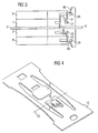
- FIG. 4 shows a cathode contact 3 and a plate 6 with a section 7, which forms the anode connection of a chip capacitor, as part of a system carrier.
- a system carrier is shown schematically in FIG.
- On one side of the system carrier of the cathode contact 3 is fixed as a flat sheet.
- On the opposite side of the cathode contact 3, a metal plate 6 is fixed, which has a portion 7.
- the section 7 of the sheet can be provided by cutting with two V-shaped depressions 41, 42 pointing in opposite directions.
- the portion 7 of the sheet 6 along the bending line 12 must be bent by 90 °.
- the V-shaped recess 41 folds up out of the plane of the sheet and the V-shaped recess 42 also folds down out of the plane of the sheet 6, whereby the anode terminal 5 shown in Figure 1 can be realized.
- FIG. 5 shows the method for producing a chip capacitor.
- a system carrier 10 is provided, with cathode contacts 3, 31, 32.
- Anode connections 5, 51, 52 are provided on the opposite side of the cathode contacts 3, 31, 32.
- the illustration in FIG. 5 is merely schematic; with regard to the exact configuration of the system carrier 10 or the cathode contacts 3, 31, 32 and the anode connections 5, 51, 52, reference is made to FIG.
- At least two capacitor carriers 11 are also provided, to which a plurality of anode contacts 21, 25, 26 are fixed in a comb-like manner, which in turn carry capacitor bodies 1, 101, 102.
- the system carrier 10 and a capacitor carrier 11 are superimposed as indicated by the arrow and then the capacitor body 1, 101, 102 are connected to cathode contacts 3, 31, 32 by fastening together.
- This attachment can be done for example by means of conductive adhesive.
- the anode contacts 21, 25, 26 are connected to the already suitably bent anode terminals 5, 51, 52. This connection is made for example by laser welding, at the same time the anode contacts 21, 25, 26 can be separated from the capacitor carrier 11, whereby at the same time the first step for separating the chip capacitors is realized.
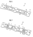
- FIG. 6 shows a system carrier 10 in which pairs of opposing metal sheets 6 and cathode contacts 3 as well as pairs of opposing metal sheets 6a and cathode contacts 3a are arranged next to one another.
- a double-row system carrier 10 is formed, in which the yield of chip capacitors can be increased again, since at the same time two capacitor carriers, coming from opposite sides of the system carrier 10 can be mounted on this.
- the system carrier 10 is provided with transport holes 13 at the edge.
- FIG. 7 shows the system carrier from FIG. 6 in a fitted state.
- the capacitor bodies 1 and 2 are mounted above and below the cathode contact 3 and connected to the anode terminal 5.
- the capacitor bodies 8 and 9 are mounted on the top and bottom of the cathode contact 3a and connected to the anode terminal 5a.
- the anode contacts 21 and 22 point in the opposite direction of the anode contacts 28, 29, which shows that two capacitor carriers can be mounted on the system carrier 10 simultaneously from the right and from the left. This is achieved by arranging the two cathode contacts 3, 3a in the inner region and the anode connections 5, 5a in the outer region of the system carrier tape 10, whereby a mirror-image arrangement is realized with respect to a longitudinal direction of the system carrier 10.
Landscapes
- Engineering & Computer Science (AREA)
- Power Engineering (AREA)
- Microelectronics & Electronic Packaging (AREA)
- Manufacturing & Machinery (AREA)
- Fixed Capacitors And Capacitor Manufacturing Machines (AREA)
- Organic Low-Molecular-Weight Compounds And Preparation Thereof (AREA)
Description
- Die Erfindung betrifft einen Chipkondensator mit wenigstens zwei Kondensatorkörpern, die jeweils mit einem Anodenkontakt versehen sind. Ferner betrifft die Erfindung ein Verfahren zur Herstellung des Kondensators.
- Es sind aus der Druckschrift US 3,686,535 Chipkondensatoren der eingangs genannten Art bekannt, bei denen wenigstens zwei Kondensatorkörper mit ihren Flachseiten an einem Kathodenkontakt befestigt sind.
- Die bekannten Chipkondensatoren haben den Nachteil, daß für die Montage des Kondensator mit mehreren Kondensatorkörpern jeder Kondensatorkörper einzeln mittels einer sogenannten Pick-and-Place-Vorrichtung auf den Kathodenkontakt aufgesetzt wird. Anschließend wird jeder Kondensatorkörper einzeln mit einem Leadframe verbunden.
- Diese Vorgehensweise für die Herstellung des Chipkondensators ist zeitaufwendig, da jeder Kondensatorkörper einzeln montiert werden muß.
- Es ist Aufgabe der vorliegenden Erfindung, einen Chipkondensator anzugeben, der einfach und schnell herstellbar ist. Es ist ferner Aufgabe der vorliegenden Erfindung, ein Verfahren zur Herstellung des Chipkondensators anzugeben.
- Diese Aufgaben werden gelöst durch einen Chipkondensator gemäß Patentanspruch 1 beziehungsweise durch ein Verfahren gemäß Patentanspruch 11. Weitere Ausgestaltungen der Erfindung sind den abhängigen Patentansprüchen zu entnehmen.
- Es wird ein Chipkondensator angegeben mit wenigstens zwei Kondensatorkörpern, die jeweils mit einem Anodenkontakt versehen sind. Der Anodenkontakt ragt aus dem Inneren des Kontaktkörpers heraus. Ferner weist der Chipkondensator einen Kathodenkontakt auf. Die Kondensatorkörper sind übereinander gestapelt und auf dem Kathodenkörper montiert. Dabei ist wenigstens ein Kondensatorkörper mit einer breiten Seite versehen, die auf dem Kathodenkontakt montiert ist.
- Durch die Montage wenigstens eines Kondensatorkörpers mit der Breitseite auf den Kathodenkontakt und durch das Übereinanderstapeln von Kondensatorkörpern ist es möglich, den Chipkondensator mittels eines Verfahrens herzustellen, welches die Herstellung einer Vielzahl von Chipkondensatoren zur gleichen Zeit erlaubt. Die Kondensatorkörper brauchen dann nämlich nicht mehr einzeln mit dem Kathodenkontakt verbunden werden, sondern es können eine Vielzahl von Kondensatorkörpern gleichzeitig mit einem Kathodenkontakt verbunden werden. Darüber hinaus ermöglicht die Anordnung von Anodenkontakt und Kathodenkontakt die Herstellung von Chipkondensatoren, die wenigstens zwei Kondensatorkörper enthalten, welche innerhalb des Chipkondensators parallel geschaltet werden können. Eine solche Parallelschaltung mehrerer Kondensatorkörper innerhalb des Chipkondensators hat den Vorteil, daß der Chipkondensator einen niedrigeren elektrischen Serienwiderstand aufweist.
- Es wird ein Verfahren zur Herstellung eines Chipkondensators angegeben, wobei in einem ersten Schritt ein Systemträger bereitgestellt wird. Der Systemträger weist aneinandergereihte Kathodenkontakte auf. Gegenüber den Kathodenkontakten ist jeweils ein Anodenanschluß am Systemträger angeordnet. Ferner wird eine Vielzahl von Kondensatorkörpern bereitgestellt, die jeweils mit einem Anodenkontakt versehen sind. Jeder der Anodenkontakte ragt aus dem Kondensatorkörper heraus. Die Kondensatorkörper sind mittels der Anodenkontakte kammartig mit einem gemeinsamen Kondensatorträger verbunden. Es wird eine Vielzahl - wenigstens jedoch zwei - solcher Kondensatorträger bereitgestellt.
- In einem weiteren Schritt werden der Systemträger und ein erster Kondensatorträger übereinandergelegt.
- Es werden Kondensatorkörper am entsprechenden Kathodenkontakt befestigt. Es werden auch Anodenkontakte am entsprechenden Anodenanschluß des Systemträgers befestigt.
- In einem weiteren Schritt wird der Systemträger und ein weiterer Kondensatorträger übereinandergelegt. Es werden Kondensatorkörper an Zusammenbauten aus einem Kondensatorkörper und einem Kathodenkontakt befestigt. Es werden ferner Anodenkontakte an entsprechenden Anodenanschlüssen des Systemträgers befestigt.
- Das Verfahren hat den Vorteil, daß eine Vielzahl von Anodenkörpern gleichzeitig an Kathodenkontakten befestigt wird. Darüber hinaus hat das Verfahren den Vorteil, daß eine Vielzahl von Chipkondensatoren mit mehreren Kondensatorkörpern gleichzeitig herstellbar ist.
- Die Befestigung des Kondensatorkörpers am Kathodenkontakt kann vorteilhafterweise mittels eines Leitklebers erfolgen. Ebenfalls kann ein Kondensatorkörper an einem weiteren Kondensatorkörper mittels Leitkleber befestigt sein. Der Leitkleber hat den Vorteil, daß er einfach zu verarbeiten ist und daß er neben der Haftung von zwei Teilen aneinander auch noch einen guten elektrischen Kontakt vermittelt.
- Anodenkontakte können in Vertiefungen eines Anodenanschlusses angeordnet sein. Dadurch erreicht man den Vorteil, daß die Anodenkontakte örtlich fixiert sind, was den Zusammenbau des Chipkondensators erleichtert.
- Die Vertiefungen können desweiteren vorteilhafterweise zu der dem Kathodenkontakt gegenüberliegenden Seite des jeweiligen Kontaktkörpers hin offen sein. Dadurch wird es erleichtert, den Kondensatorkörper von einer Montageoberseite her an der gewünschten Position, entweder auf dem Kathodenkontakt oder auf einem bereits im Chipkondensator vorhandenen Kondensatorkörper, zu positionieren und gleichzeitig den Anodenkontakt an seiner bestimmungsgemäßen Position am Anodenanschluß einzuführen.
- In einer vorteilhaften Ausführungsform der Erfindung sind die Vertiefungen V-förmig aus einem Abschnitt eines Blechs herausgeschnitten. Der Abschnitt des Blechs ist senkrecht aus der Ebene des Blechs herausgebogen. Das Blech verläuft parallel zum Kathodenkontakt, während der Abschnitt mit den V-förmigen Ausschnitten zumindest annähernd senkrecht zum Kathodenkontakt verläuft. Indem der Kathodenkontakt und das Blech, das einen Teil des Anodenanschlusses bildet, zumindest annähernd parallel zueinander verlaufen, wird es ermöglicht, den Kathodenkontakt und den Anodenanschluß als Teile eines Systemträgers zu bilden, was die gleichzeitig die herstellbare Stückzahl von Chipkondensatoren maßgeblich steigert.
- Die Kondensatorkörper können auf verschiedenen Seiten des Kathodenkontakts befestigt sein. Dadurch läßt sich ein symmetrischer Aufbau des Chipkondensators realisieren, der eine hohe mechanische Festigkeit aufweist.
- In einer anderen Ausführungsform der Erfindung können die Kondensatorkörper übereinandergestapelt und auf ein und derselben Seite des Kathodenkontakts befestigt sein. Dadurch wird es ermöglicht, die Kondensatorkörper immer von einer Seite her auf den Kathodenkontakt zu montieren. Dies erleichtert die Montage, da ein Umdrehen des Kathodenkontakts nicht mehr erforderlich ist.
- Um auch bei auf derselben Seite des Kathodenkontakts übereinanderliegenden Kondensatorkörpern ein sicheres Einführen des Anodenkontakts in die V-förmige Vertiefung zu erreichen, ist es vorteilhaft, wenn die auf derselben Seite des Kathodenkontakts angeordneten Anodenkontakte seitlich zueinander versetzt sind, so daß jeder Anodenkontakt freien Zugang in seine für ihn vorgesehene V-förmige Vertiefung hat.
- Hingegen können die Anodenkontakte von zwei auf verschiedenen Seiten des Kathodenkontakts montierten Kondensatorkörpern senkrecht übereinanderliegend angeordnet sein, was die Designvielfalt des Kondensatorkörpers reduziert und somit die Herstellung vereinfacht und damit verbilligt.
- In einer vorteilhaften Ausführungsform der Erfindung können die Anodenkontakte in den Vertiefungen mittels Laserschweißen befestigt sein. Das Befestigen der Anodenkontakte in Vertiefungen mittels Laserschweißen hat den Vorteil, daß durch das Laserschweißen gleichzeitig noch die Trennung des Kondensatorkörpers vom Kondensatorträger bewerkstelligt werden kann, wodurch die Vereinzelung gleichzeitig mit erfolgt.
- Es ist demnach ein Verfahren vorteilhaft, wobei die Befestigung der Kondensatorkörper des weiteren Kondensatorträgers jeweils auf dem Kondensatorkörper des ersten Kondensatorträgers erfolgt. Daraus resultiert ein Chipkondensator mit übereinandergestapelten Kondensatorkörpern, die nur auf einer Seite des Kathodenkontakts befestigt sind.
- Im folgenden wird die Erfindung anhand von Ausführungsbeispielen und den dazugehörigen Figuren näher erläutert.
- Figur 1
- zeigt beispielhaft einen Chipkondensator während der Herstellung in einer perspektivischen Seitenansicht.
- Figur 2
- zeigt beispielhaft einen weiteren erfindungsgemäßen Chipkondensator in einer perspektivischen Seitenansicht.
- Figur 3
- zeigt beispielhaft einen weiteren erfindungsgemäßen Chipkondensator in einer perspektivischen Seitenansicht.
- Figur 4
- zeigt einen Ausschnitt eines Systemträgers, wie er zur Herstellung des erfindungsgemäßen Chipkondensators beziehungsweise zur Verwendung im erfindungsgemäßen Verfahren verwendet werden kann.
- Figur 5
- zeigt beispielhaft ein erfindungsgemäßes Verfahren zur Herstellung eines Chipkondensators.
- Figur 6
- zeigt beispielhaft einen unbestückten Systemträger, geeignet zur Durchführung des Herstellungsverfahrens in Draufsicht.
- Figur 7
- zeigt den Systemträger aus Figur 6 in bestücktem Zustand.
- Figur 1 zeigt einen Chipkondensator mit zwei Kondensatorkörpern 1, 2. Die Kondensatorkörper 1, 2 haben die Form von Quadern. Die breiten Seiten der Kondensatorkörper 1, 2, sind auf der Oberseite beziehungsweise der Unterseite eines blechförmigen Kathodenkontakts 3 mittels eines Leitklebers befestigt.
- Aus dem Innern der Kondensatorkörper 1, 2 sind Anodenkontakte 21, 22 herausgeführt. Die Anodenkontakte 21, 22 sind in V-förmigen Vertiefungen 41, 42 angeordnet. Sie sind dort durch Laserschweißen befestigt. Die Vertiefungen 41, 42 sind aus einem Abschnitt 7 eines Blechs 6 herausgeschnitten. Die Vertiefung 41 öffnet sich dabei zur Oberseite des Kathodenkontakts 3 während sich die Vertiefung 42 zur Unterseite des Kathodenkontakts 3 hin öffnet. Dadurch können die Anodenkontakte 21, 22 der Kondensatorkörper 1, 2 leicht in die Vertiefungen 41, 42 eingelegt werden und so auf dem Kathodenkontakt 3 von der Oberseite beziehungsweise von der Unterseite her montiert werden. Der die Vertiefungen 41, 42 tragende Abschnitt 7 des Bleches 6 ist um ca. 90° gegenüber der Montageebene gekippt. Diese Kippung erreicht man durch Biegen eines Blechs 6, wie es in Figur 4 als Teil eines Systemträgers dargestellt ist. Die V-förmigen Vertiefungen 41, 42 haben darüber hinaus den Vorteil, daß sie zur Justierung der Anodenkontakte 21, 22 verwendet werden können.
- In Figur 1 sind die Kondensatorkörper 1, 2 auf verschiedenen Seiten des flächig gebildeten Kathodenkontaktes 3 befestigt.
- Gemäß Figur 2 sind die Kondensatorkörper 1, 2 auf derselben Seite eines Kathodenkontakts 3 befestigt. Dabei bilden die Kondensatorkörper 1, 2 einen Stapel von jeweils mit ihren breiten Seitenflächen übereinander und auch über dem Kathodenkontakt 3 liegenden Kondensatorkörpern 1, 2.
- Die Kondensatorkörper 1, 2 sind durch elektrisch leitfähigen Kleber, beispielsweise Leitsilber, aneinander befestigt. Der Stapel aus Kondensatorkörpern 1, 2 wiederum ist durch Leitkleber am Kathodenkontakt 3 befestigt. Die aus dem Innern der Kondensatorkörper 1, 2 herausragenden Anodenkontakte 21, 22 sind seitlich gegeneinander versetzt, so daß jeder für sich in eine V-förmige Vertiefung 41, 42 eingreifen kann, die in der geeigneten Höhe am Abschnitt 7 des Bleches 6 angeordnet ist. Der Abschnitt 7 des Bleches 6 bildet ebenso wie in Figur 1 den Anodenanschluß 5 des herzustellenden Chipkondensators.
- Die Kondensatorkörper 1, 2 können beispielsweise an sich bekannte Sinterkörper aus Tantalpulver sein, bei denen mittels der bekannten Methoden ein Elektrolytkondensator mit einer außenliegenden Kathodenelektrode hergestellt wird. Beispielsweise wird dabei als Anodenkontakt ein Tantaldraht verwendet. Dieser wir von Tantalpulver umpresst, gesintert und anschließend durch Oxidation mit einem Dielektrikum versehen. Die Kathodenschicht besteht aus Mangandioxid, welches in einem Pyrolyseprozess aus Mangannitrat erzeugt wird. Weitere Schichten aus Graphit und Silberlack dienen als Kontaktschichten.
- Es kommen jedoch auch Kondensatorkörper in Betracht, die anstelle von Tantal Niob bzw. anstelle von Mangandioxid Polymer enthalten.
- Figur 3 zeigt einen weiteren Kondensator während der Herstellung, wobei zu beiden Seiten eines Kathodenkontakts 3 jeweils zwei Kondensatorkörper 1, 8 sowie 2, 9 befestigt sind. Ein Abschnitt 7 des Bleches 6 ist dabei mit insgesamt vier V-förmigen Vertiefungen 41, 42, 48, 49 versehen, die jeweils in einer speziell für einen Kondensatorkörper 1, 2, 8, 9 geeigneten Höhe angeordnet sind. Die Kondensatorkörper 1, 2, 8, 9 sind mit Anodenkontakten 21, 22, 28, 29 versehen, die in die entsprechende Vertiefung 41, 42, 48, 49 eingreifen.
- Figur 4 zeigt einen Kathodenkontakt 3 sowie ein Blech 6 mit einem Abschnitt 7, der den Anodenanschluß eines Chipkondensators bildet, als Bestandteil eines Systemträgers. Ein solcher Systemträger ist schematisch in Figur 5 dargestellt. An einer Seite des Systemträgers ist der Kathodenkontakt 3 als flaches Blech befestigt. Auf der gegenüberliegenden Seite des Kathodenkontakts 3 ist ein Blech 6 befestigt, welches einen Abschnitt 7 aufweist. Der Abschnitt 7 des Blechs kann durch Schneiden mit zwei in entgegengesetzte Richtungen zeigenden V-förmigen Vertiefungen 41, 42 versehen werden. Um den Abschnitt 7 in eine Position zu bringen, in der er zur Aufnahme von Anodenkontakten 21, 22 von Kondensatorkörpern eines Chipkondensators geeignet ist, muß lediglich der Abschnitt 7 des Bleches 6 entlang der Biegelinie 12 um 90° abgebogen werden. Dadurch klappt die V-förmige Vertiefung 41 nach oben aus der Blechebene heraus und die V-förmige Vertiefung 42 klappt nach unten ebenfalls aus der Ebene des Bleches 6 heraus, wodurch der in Figur 1 dargestellte Anodenanschluß 5 realisiert werden kann.
- Figur 5 zeigt das Verfahren zur Herstellung eines Chipkondensators. Es wird ein Systemträger 10 bereitgestellt, mit Kathodenkontakten 3, 31, 32. Auf der gegenüberliegenden Seite der Kathodenkontakte 3, 31, 32 sind Anodenanschlüsse 5, 51, 52 vorgesehen. Die Darstellung in Figur 5 ist lediglich schematisch, bezüglich der genauen Ausgestaltung des Systemträgers 10 beziehungsweise der Kathodenkontakte 3, 31, 32 und der Anodenanschlüsse 5, 51, 52 wird auf Figur 4 verwiesen.
- Es werden auch mindestens zwei Kondensatorträger 11 bereitgestellt, an denen kammartig eine Vielzahl von Anodenkontakten 21, 25, 26 befestigt sind, die ihrerseits wiederum Kondensatorkörper 1, 101, 102 tragen. Der Systemträger 10 und ein Kondensatorträger 11 werden wie durch den Pfeil angedeutet übereinandergelegt und anschließend werden die Kondensatorkörper 1, 101, 102 mit Kathodenkontakten 3, 31, 32 durch Befestigen miteinander verbunden. Diese Befestigung kann beispielsweise mittels Leitkleber erfolgen. Ebenfalls werden die Anodenkontakte 21, 25, 26 mit den bereits geeignet gebogenen Anodenanschlüssen 5, 51, 52 verbunden. Diese Verbindung erfolgt beispielsweise durch Laserschweißen, wobei gleichzeitig die Anodenkontakte 21, 25, 26 vom Kondensatorträger 11 getrennt werden können, womit gleichzeitig der erste Schritt zum Vereinzeln der Chipkondensatoren realisiert wird.
- Figur 6 zeigt einen Systemträger 10, bei dem Paare von gegenüberliegenden Blechen 6 und Kathodenkontakten 3 sowie Paare von gegenüberliegenden Blechen 6a und Kathodenkontakten 3a nebeneinander angeordnet sind. Somit wird ein zweireihiger Systemträger 10 gebildet, bei dem die Ausbeute an Chipkondensatoren nochmals erhöht werden kann, da gleichzeitig zwei Kondensatorträger, kommend von gegenüberliegenden Seiten des Systemträgers 10 auf diesem aufmontiert werden können. Der Systemträger 10 ist am Rand mit Transportlöchern 13 versehen.
- Figur 7 zeigt den Systemträger aus Figur 6 in bestücktem Zustand. Auf der linken Hälfte des Systemträgers 10 sind die Kondensatorkörper 1 und 2 oberhalb bzw. unterhalb des Kathodenkontakts 3 montiert und mit dem Anodenanschluß 5 verbunden. Auf der rechten Hälfte sind die Kondensatorkörper 8 und 9 auf der Oberseite bzw. Unterseite des Kathodenkontakts 3a montiert und mit dem Anodenanschluß 5a verbunden. Die Anodenkontakte 21 und 22 zeigen in die entgegengesetzte Richtung der Anodenkontakte 28, 29, was zeigt, daß zwei Kondensatorträger gleichzeitig von rechts und von links auf den Systemträger 10 aufmontiert werden können. Dies wird erreicht, indem die beiden Kathodenkontakte 3, 3a im inneren Bereich und die Anodenanschlüsse 5, 5a im äußeren Bereich des Systemträgerbandes 10 angeordnet sind, wodurch bezüglich einer Längsrichtung des Systemträgers 10 eine spiegelbildliche Anordnung verwirklicht wird.
- Es wird darauf hingewiesen, daß die Verfahrensschritte bezüglich des Befestigens der Kondensatorkörper auf den Kathodenkontakten beziehungsweise der Anodenanschlüsse in beliebiger Reihenfolge durchgeführt werden können.
-
- 1, 2, 8, 9, 101, 102
- Kondensatorkörper
- 21, 22, 28, 29, 25, 26
- Anodenkontakt
- 3, 31, 32, 3a
- Kathodenkontakt
- 41, 42, 48, 49
- Vertiefungen
- 5, 51, 52, 5a
- Anodenanschluß
- 6, 6a
- Blech
- 7
- Abschnitt
- 10
- Systemträger
- 11
- Kondensatorträger
- 12
- Biegelinie
- 13
- Transportloch
Claims (15)
- Chipkondensator- mit wenigstens zwei Kondensatorkörpern (1, 2),- die jeweils mit einem Anodenkontakt (21, 22) versehen sind, der aus dem Kondensatorkörper (1, 2) herausragt,- und mit einem Kathodenkontakt (3),- bei dem die Kondensatorkörper (1, 2) übereinandergestapelt und bei dem eine breite Seite wenigstens eines Kondensatorkörpers (1, 2) auf dem Kathodenkontakt (3) montiert ist.
- Chipkondensator nach Anspruch 1,
bei dem ein Kondensatorkörper (1) mittels Leitkleber mit dem Kathodenkontakt (3) verklebt ist. - Chipkondensator nach einem der Ansprüche 1 oder 2,
bei dem ein Kondensatorkörper (2) mittels Leitkleber mit einem weiteren Kondensatorkörper (1) verklebt ist. - Chipkondensator nach einem der Ansprüche 1 bis 3,
bei dem die Anodenkontakte (21, 22) in Vertiefungen (41, 42) eines Anodenanschlusses (5) angeordnet sind. - Chipkondensator nach Anspruch 4,
bei dem die Vertiefungen (41, 42) zu der dem Kathodenkontakt (3) gegenüberliegenden Seite des jeweiligen Kondensatorkörpers (21, 22) hin offen sind. - Chipkondensator nach einem der Ansprüche 4 bis 5,
bei dem die Vertiefungen (41, 42) V-förmig aus einem Abschnitt (7) eines Blechs (6) herausgeschnitten sind, der senkrecht aus der Ebene des Blechs (6) herausgebogen ist, welche parallel zum Kathodenkontakt (3) verläuft. - Chipkondensator nach einem der Ansprüche 1 bis 6,
bei dem die Kondensatorkörper (1, 2) auf verschiedenen Seiten des Kathodenkontakts (3) befestigt sind. - Chipkondensator nach einem der Ansprüche 1 bis 6,
bei dem Kondensatorkörper (1, 2) auf derselben Seite des Kathodenkontakts (3) befestigt sind. - Chipkondensator nach einem der Ansprüche 1 bis 8,
bei dem Anodenkontakte (21, 28; 24, 29) seitlich zueinander versetzt angeordnet sind. - Chipkondensator nach einem der Ansprüche 4 bis 9,
bei dem die Anodenkontakte (21, 22, 28, 29) in den Vertiefungen (41, 42, 48, 49) mittels Laserschweißen befestigt sind. - Verfahren zur Herstellung eines Chipkondensators mit folgenden Schritten:a) Bereitstellen eines Systemträgers (10) mit aneinandergereihten Kathodenkontakten (3, 31, 32), denen jeweils ein Anodenanschluß (5, 51, 52) gegenüberliegt,
sowie einer Vielzahl von Kondensatorträgern (11), an denen jeweils eine Vielzahl von Kondensatorkörpern (1, 101, 102) kammartig mittels aus jedem Kondensatorkörper (1, 101, 102) herausragenden Anodenkontakten (21, 25, 26) befestigt sindb) Übereinanderlegen von Systemträger (10) und einem ersten Kondensatorträger (11) und Befestigen von Kondensatorkörpern (1, 101, 102) an Kathodenkontakten (3, 31, 32) und Befestigen von Anodenkontakten (21, 25, 26) an Anodenanschlüssen (5, 51, 52),c) Übereinanderlegen von Systemträger (10) und eines weiteren Kondensatorträgers (11) und Befestigen von Kondensatorkörpern (1, 101, 102) an Zusammenbauten aus Kondensatorkörper (1, 101, 102) und Kathodenkontakt (3, 31, 32) sowie Befestigen von Anodenkontakten (21, 25, 26) an Anodenanschlüssen (5, 51, 52). - Verfahren nach Anspruch 11,
wobei die Befestigung von Kondensatorkörpern (1, 101, 102) des ersten und weiteren Kondensatorträgers (11) zu beiden Seiten eines Kathodenkontakts (3, 31, 32) erfolgt. - Verfahren nach Anspruch 11,
wobei die Befestigung von Kondensatorkörpern (1, 101, 102) des weiteren Kontaktträgers (11) auf Kondensatorkörpern (1, 101, 102) des ersten Kondensatorträgers (11) erfolgt. - Verfahren nach einem der Ansprüche 11 bis 13,
wobei die Befestigung der Kondensatorkörper (1, 101, 102) auf Kathodenkontakten (3, 31, 32) mittels eines Leitklebers erfolgt. - Verfahren nach einem der Ansprüche 11 bis 14,
wobei die Befestigung der Anodenkontakte (21, 25, 26) an Anodenanschlüssen (5, 51, 52) mittels Laserschweißen unter gleichzeitiger Trennung des Anodenkontakts (21, 25, 26) vom Kondensatorträger (11) erfolgt.
Applications Claiming Priority (3)
| Application Number | Priority Date | Filing Date | Title |
|---|---|---|---|
| DE10222405A DE10222405B4 (de) | 2002-05-21 | 2002-05-21 | Chipkondensator und Verfahren zu dessen Herstellung |
| DE10222405 | 2002-05-21 | ||
| PCT/DE2003/001646 WO2003098647A2 (de) | 2002-05-21 | 2003-05-21 | Chipkondensator und verfahren zu dessen herstellung |
Publications (2)
| Publication Number | Publication Date |
|---|---|
| EP1506557A2 EP1506557A2 (de) | 2005-02-16 |
| EP1506557B1 true EP1506557B1 (de) | 2006-08-23 |
Family
ID=29432174
Family Applications (1)
| Application Number | Title | Priority Date | Filing Date |
|---|---|---|---|
| EP03752708A Expired - Lifetime EP1506557B1 (de) | 2002-05-21 | 2003-05-21 | Chipkondensator und verfahren zu dessen herstellung |
Country Status (9)
| Country | Link |
|---|---|
| US (1) | US7190571B2 (de) |
| EP (1) | EP1506557B1 (de) |
| JP (1) | JP2005526391A (de) |
| KR (1) | KR20040111666A (de) |
| CN (1) | CN100538939C (de) |
| AT (1) | ATE337607T1 (de) |
| DE (3) | DE10222405B4 (de) |
| TW (1) | TWI223293B (de) |
| WO (1) | WO2003098647A2 (de) |
Families Citing this family (20)
| Publication number | Priority date | Publication date | Assignee | Title |
|---|---|---|---|---|
| EP1654745B1 (de) * | 2003-08-13 | 2012-08-01 | Showa Denko K.K. | Chip-festelektrolytkondensator und herstellungsverfahren dafür |
| TWI402873B (zh) * | 2005-01-24 | 2013-07-21 | 松下電器產業股份有限公司 | Chip type solid electrolytic capacitors |
| DE102005007582A1 (de) * | 2005-02-18 | 2006-08-24 | Epcos Ag | Kondensator mit einem niedrigen Ersatzserienwiderstand und Kondensatoranordung |
| US7916457B2 (en) * | 2005-05-13 | 2011-03-29 | Sanyo Electric Co., Ltd. | Multi-layered solid electrolytic capacitor and method of manufacturing same |
| US7352563B2 (en) * | 2006-03-13 | 2008-04-01 | Avx Corporation | Capacitor assembly |
| US7468882B2 (en) * | 2006-04-28 | 2008-12-23 | Avx Corporation | Solid electrolytic capacitor assembly |
| WO2007130483A2 (en) * | 2006-05-05 | 2007-11-15 | Cabot Corporation | Tantalum powder with smooth surface and methods of manufacturing same |
| USD586767S1 (en) * | 2007-02-26 | 2009-02-17 | Kemet Electronics Corporation | Anodes |
| JP5142772B2 (ja) * | 2008-03-12 | 2013-02-13 | 三洋電機株式会社 | 固体電解コンデンサ |
| US8430944B2 (en) * | 2008-12-22 | 2013-04-30 | Global Advanced Metals, Usa, Inc. | Fine particle recovery methods for valve metal powders |
| US8125769B2 (en) | 2010-07-22 | 2012-02-28 | Avx Corporation | Solid electrolytic capacitor assembly with multiple cathode terminations |
| US8259436B2 (en) | 2010-08-03 | 2012-09-04 | Avx Corporation | Mechanically robust solid electrolytic capacitor assembly |
| JP5796195B2 (ja) * | 2011-01-12 | 2015-10-21 | パナソニックIpマネジメント株式会社 | 固体電解コンデンサ |
| CN105417110B (zh) * | 2015-12-10 | 2017-06-16 | 重庆凯西驿电子科技有限公司 | 一种专用于电容器的传输装置 |
| DE102016011610B3 (de) * | 2016-09-26 | 2018-08-09 | Hottinger Baldwin Messtechnik Gmbh | Anschweißbarer Dehnungssensor für gekrümmte Oberflächen |
| KR102389784B1 (ko) | 2018-03-05 | 2022-04-22 | 글로벌 어드밴스드 메탈스 유에스에이, 아이엔씨. | 구형 분말을 함유하는 애노드 및 커패시터 |
| JP7383300B2 (ja) | 2018-03-05 | 2023-11-20 | グローバル アドバンスト メタルズ ユー.エス.エー.,インコーポレイティド | 粉末冶金スパッタリングターゲット及びその製造方法 |
| CA3091448C (en) | 2018-03-05 | 2024-03-19 | Craig Sungail | Spherical tantalum powder, products containing the same, and methods of making the same |
| KR102527716B1 (ko) * | 2018-11-22 | 2023-05-02 | 삼성전기주식회사 | 탄탈륨 커패시터 |
| KR20210100674A (ko) | 2018-12-12 | 2021-08-17 | 글로벌 어드밴스드 메탈스 유에스에이, 아이엔씨. | 구형 니오브 합금 분말, 그를 함유하는 생성물, 및 그의 제조 방법 |
Family Cites Families (29)
| Publication number | Priority date | Publication date | Assignee | Title |
|---|---|---|---|---|
| GB1328780A (en) * | 1971-05-26 | 1973-09-05 | Matsuo Electric Co | Method of manufacturing capacitors |
| US3686535A (en) * | 1971-07-02 | 1972-08-22 | Union Carbide Corp | Electrolytic capacitor with separate interconnected anode bodies |
| US4097916A (en) * | 1976-06-28 | 1978-06-27 | Union Carbide Corporation | Electrolytic capacitor lead terminal configuration |
| US4282645A (en) * | 1978-07-31 | 1981-08-11 | Sprague Electric Company | Method of assembling an encapsulated chip capacitor |
| JPS6027177B2 (ja) * | 1980-04-02 | 1985-06-27 | 松下電器産業株式会社 | チップ状固体電解コンデンサおよびその製造方法 |
| US4581479A (en) * | 1984-11-16 | 1986-04-08 | Moore Theodore W | Dimensionally precise electronic component mount |
| JPH0191411A (ja) * | 1987-10-02 | 1989-04-11 | Hitachi Condenser Co Ltd | 複合コンデンサ |
| DE3931249C2 (de) * | 1989-09-19 | 1993-10-21 | Siemens Ag | Festelektrolytkondensator in Chip-Bauweise |
| DE3931244A1 (de) * | 1989-09-19 | 1991-03-28 | Siemens Ag | Verfahren zum herstellen eines festelektrolytkondensators in chip-bauweise |
| JPH05205984A (ja) * | 1992-01-27 | 1993-08-13 | Nec Corp | 積層型固体電解コンデンサ |
| JP2998440B2 (ja) * | 1992-08-19 | 2000-01-11 | 日本電気株式会社 | 積層型固体電解コンデンサ |
| JPH0684716A (ja) * | 1992-08-31 | 1994-03-25 | Nippon Chemicon Corp | 固体電解コンデンサの製造方法 |
| JPH07105317B2 (ja) * | 1992-11-30 | 1995-11-13 | 日本電気株式会社 | 積層型固体電解コンデンサとその製造方法 |
| JPH07240351A (ja) | 1994-02-28 | 1995-09-12 | Matsushita Electric Ind Co Ltd | 電解コンデンサ |
| JP3557564B2 (ja) * | 1994-10-12 | 2004-08-25 | 昭和電工株式会社 | 積層型固体電解コンデンサ |
| EP0823719B1 (de) * | 1996-07-26 | 2002-06-05 | Nec Corporation | Festelektrolytkondensator mit vorplattierten Leiteranschlüssen und dessen Herstellungsverfahren |
| JPH11274003A (ja) * | 1998-03-25 | 1999-10-08 | Nichicon Corp | チップ型積層固体電解コンデンサ |
| CN1154134C (zh) * | 1998-06-11 | 2004-06-16 | 昭和电工株式会社 | 单板电容器元件和叠层型固体电解电容器 |
| JP3536722B2 (ja) * | 1998-06-18 | 2004-06-14 | 松下電器産業株式会社 | チップ形固体電解コンデンサおよびその製造方法 |
| JP3755336B2 (ja) * | 1998-08-26 | 2006-03-15 | 松下電器産業株式会社 | 固体電解コンデンサおよびその製造方法 |
| US6421227B2 (en) * | 1999-12-10 | 2002-07-16 | Showa Denko K.K. | Solid electrolytic multilayer capacitor |
| JP3349133B2 (ja) * | 2000-04-07 | 2002-11-20 | エヌイーシートーキン株式会社 | チップ型コンデンサ及びその製造方法並びにモールド金型 |
| TW516054B (en) * | 2000-05-26 | 2003-01-01 | Matsushita Electric Industrial Co Ltd | Solid electrolytic capacitor |
| DE10131236B4 (de) | 2001-06-28 | 2006-03-30 | Epcos Ag | Kondensator |
| JP2003068576A (ja) * | 2001-08-30 | 2003-03-07 | Rohm Co Ltd | 面実装型固体電解コンデンサの構造及びその製造方法 |
| JP4477287B2 (ja) * | 2002-03-15 | 2010-06-09 | Necトーキン株式会社 | 陽極端子板およびチップ型コンデンサの製造方法 |
| TWI226648B (en) | 2002-07-18 | 2005-01-11 | Epcos Ag | Surface-mountable component and its production method |
| DE10244713A1 (de) | 2002-07-18 | 2004-02-05 | Epcos Ag | Oberflächenmontierbares Bauelement und Verfahren zu dessen Herstellung |
| JP4472277B2 (ja) * | 2003-04-10 | 2010-06-02 | Necトーキン株式会社 | チップ型固体電解コンデンサ |
-
2002
- 2002-05-21 DE DE10222405A patent/DE10222405B4/de not_active Expired - Fee Related
- 2002-05-21 DE DE10262263A patent/DE10262263B4/de not_active Expired - Fee Related
-
2003
- 2003-05-07 TW TW092112421A patent/TWI223293B/zh active
- 2003-05-21 JP JP2004506050A patent/JP2005526391A/ja not_active Withdrawn
- 2003-05-21 US US10/514,788 patent/US7190571B2/en not_active Expired - Fee Related
- 2003-05-21 AT AT03752708T patent/ATE337607T1/de not_active IP Right Cessation
- 2003-05-21 CN CNB03811626XA patent/CN100538939C/zh not_active Expired - Fee Related
- 2003-05-21 KR KR10-2004-7018739A patent/KR20040111666A/ko not_active Ceased
- 2003-05-21 WO PCT/DE2003/001646 patent/WO2003098647A2/de not_active Ceased
- 2003-05-21 EP EP03752708A patent/EP1506557B1/de not_active Expired - Lifetime
- 2003-05-21 DE DE50304758T patent/DE50304758D1/de not_active Expired - Lifetime
Also Published As
| Publication number | Publication date |
|---|---|
| TW200403697A (en) | 2004-03-01 |
| KR20040111666A (ko) | 2004-12-31 |
| DE10222405A1 (de) | 2003-12-18 |
| CN100538939C (zh) | 2009-09-09 |
| ATE337607T1 (de) | 2006-09-15 |
| WO2003098647A3 (de) | 2004-04-29 |
| CN1656582A (zh) | 2005-08-17 |
| DE10262263B4 (de) | 2008-12-04 |
| EP1506557A2 (de) | 2005-02-16 |
| WO2003098647A2 (de) | 2003-11-27 |
| DE10222405B4 (de) | 2007-09-27 |
| TWI223293B (en) | 2004-11-01 |
| US7190571B2 (en) | 2007-03-13 |
| US20050174719A1 (en) | 2005-08-11 |
| DE50304758D1 (de) | 2006-10-05 |
| JP2005526391A (ja) | 2005-09-02 |
Similar Documents
| Publication | Publication Date | Title |
|---|---|---|
| DE10222405B4 (de) | Chipkondensator und Verfahren zu dessen Herstellung | |
| DE3319311C2 (de) | Verfahren zur Herstellung eines elektroakustischen Wandlers mit feststehender Elektrode und dieser gegenüberstehender Membran | |
| DE2728057C2 (de) | Festelektrolytkondensator mit einem porösen Anodenkörper aus Ventilmetall | |
| DE69404291T2 (de) | Verbesserungen bezueglich elektrochemischer zellen | |
| DE4317125C2 (de) | Monolithische Mehrschicht-Chip-Induktivität | |
| DE1566981A1 (de) | Halbleitereinheit und Verfahren zu deren Herstellung | |
| EP0115803A2 (de) | Scheibenförmige Solarzelle | |
| DE112009001937T5 (de) | Schichttransformator für DC/DC-Umwandler | |
| DE2225825B2 (de) | Verfahren zum Herstellen einer Anzahl plättchenförmiger Festkörper-Elektrolytkondensatoren | |
| DE19628890A1 (de) | Elektronikteile mit eingebauten Induktoren | |
| DE102017210419A1 (de) | Zwischenkreiskondensator | |
| DE4312409B4 (de) | Einstellbarer Kondensator | |
| EP3232454B1 (de) | Busbar mit einer mehrzahl von filmkondensatoren | |
| DE1540488A1 (de) | Festwiderstand und Verfahren zu seiner Herstellung | |
| EP2530690B1 (de) | Elektrisches Vielschichtbauelement sowie Verfahren zur Herstellung eines elektrischen Vielschichtbauelements | |
| EP1654744B1 (de) | Kondensatormodul und verfahren zu dessen herstellung | |
| DE102008012595A1 (de) | Festelektrolytkondensator | |
| EP1523749A2 (de) | Oberflächenmontierbares bauelement und verfahren zu dessen herstellung | |
| DE102007020290A1 (de) | Gehäuse für elektrische Bauelemente und Verfahren zur Herstellung | |
| WO2014124825A1 (de) | Zellverbinder zum elektrisch leitfähigen kontaktieren einer mehrzahl von batteriezellterminals, verfahren zum herstellen eines solchen zellverbinders und batteriemodul mit wenigstens einem solchen zellverbinder | |
| EP1543534A1 (de) | Elektrisches bauelement und anordnung mit dem bauelement | |
| WO2006086972A1 (de) | Kondensator mit einem niedrigen ersatzserienwiderstand und kondensatoranordnung | |
| AT526615B1 (de) | Zellenmodul mit wiederaufladbaren Zellen | |
| EP4264689B1 (de) | Wandlerelement basierend auf dielektrischen elastomeren, verfahren zur herstellung eines wandlerelements, sowie hybrider greifer | |
| DE3238806C2 (de) | Symmetriereinrichtung |
Legal Events
| Date | Code | Title | Description |
|---|---|---|---|
| PUAI | Public reference made under article 153(3) epc to a published international application that has entered the european phase |
Free format text: ORIGINAL CODE: 0009012 |
|
| 17P | Request for examination filed |
Effective date: 20041026 |
|
| AK | Designated contracting states |
Kind code of ref document: A2 Designated state(s): AT BE BG CH CY CZ DE DK EE ES FI FR GB GR HU IE IT LI LU MC NL PT RO SE SI SK TR |
|
| GRAP | Despatch of communication of intention to grant a patent |
Free format text: ORIGINAL CODE: EPIDOSNIGR1 |
|
| RIN1 | Information on inventor provided before grant (corrected) |
Inventor name: NUNES, RUI Inventor name: HEUSMANN, HANS |
|
| GRAS | Grant fee paid |
Free format text: ORIGINAL CODE: EPIDOSNIGR3 |
|
| GRAA | (expected) grant |
Free format text: ORIGINAL CODE: 0009210 |
|
| AK | Designated contracting states |
Kind code of ref document: B1 Designated state(s): AT BE BG CH CY CZ DE DK EE ES FI FR GB GR HU IE IT LI LU MC NL PT RO SE SI SK TR |
|
| PG25 | Lapsed in a contracting state [announced via postgrant information from national office to epo] |
Ref country code: IT Free format text: LAPSE BECAUSE OF FAILURE TO SUBMIT A TRANSLATION OF THE DESCRIPTION OR TO PAY THE FEE WITHIN THE PRESCRIBED TIME-LIMIT;WARNING: LAPSES OF ITALIAN PATENTS WITH EFFECTIVE DATE BEFORE 2007 MAY HAVE OCCURRED AT ANY TIME BEFORE 2007. THE CORRECT EFFECTIVE DATE MAY BE DIFFERENT FROM THE ONE RECORDED. Effective date: 20060823 Ref country code: SK Free format text: LAPSE BECAUSE OF FAILURE TO SUBMIT A TRANSLATION OF THE DESCRIPTION OR TO PAY THE FEE WITHIN THE PRESCRIBED TIME-LIMIT Effective date: 20060823 Ref country code: RO Free format text: LAPSE BECAUSE OF FAILURE TO SUBMIT A TRANSLATION OF THE DESCRIPTION OR TO PAY THE FEE WITHIN THE PRESCRIBED TIME-LIMIT Effective date: 20060823 Ref country code: SI Free format text: LAPSE BECAUSE OF FAILURE TO SUBMIT A TRANSLATION OF THE DESCRIPTION OR TO PAY THE FEE WITHIN THE PRESCRIBED TIME-LIMIT Effective date: 20060823 Ref country code: FI Free format text: LAPSE BECAUSE OF FAILURE TO SUBMIT A TRANSLATION OF THE DESCRIPTION OR TO PAY THE FEE WITHIN THE PRESCRIBED TIME-LIMIT Effective date: 20060823 Ref country code: NL Free format text: LAPSE BECAUSE OF FAILURE TO SUBMIT A TRANSLATION OF THE DESCRIPTION OR TO PAY THE FEE WITHIN THE PRESCRIBED TIME-LIMIT Effective date: 20060823 Ref country code: IE Free format text: LAPSE BECAUSE OF FAILURE TO SUBMIT A TRANSLATION OF THE DESCRIPTION OR TO PAY THE FEE WITHIN THE PRESCRIBED TIME-LIMIT Effective date: 20060823 |
|
| REG | Reference to a national code |
Ref country code: GB Ref legal event code: FG4D Free format text: NOT ENGLISH |
|
| REG | Reference to a national code |
Ref country code: CH Ref legal event code: EP |
|
| REG | Reference to a national code |
Ref country code: IE Ref legal event code: FG4D Free format text: LANGUAGE OF EP DOCUMENT: GERMAN |
|
| REF | Corresponds to: |
Ref document number: 50304758 Country of ref document: DE Date of ref document: 20061005 Kind code of ref document: P |
|
| PG25 | Lapsed in a contracting state [announced via postgrant information from national office to epo] |
Ref country code: SE Free format text: LAPSE BECAUSE OF FAILURE TO SUBMIT A TRANSLATION OF THE DESCRIPTION OR TO PAY THE FEE WITHIN THE PRESCRIBED TIME-LIMIT Effective date: 20061123 Ref country code: BG Free format text: LAPSE BECAUSE OF FAILURE TO SUBMIT A TRANSLATION OF THE DESCRIPTION OR TO PAY THE FEE WITHIN THE PRESCRIBED TIME-LIMIT Effective date: 20061123 Ref country code: DK Free format text: LAPSE BECAUSE OF FAILURE TO SUBMIT A TRANSLATION OF THE DESCRIPTION OR TO PAY THE FEE WITHIN THE PRESCRIBED TIME-LIMIT Effective date: 20061123 |
|
| PG25 | Lapsed in a contracting state [announced via postgrant information from national office to epo] |
Ref country code: ES Free format text: LAPSE BECAUSE OF FAILURE TO SUBMIT A TRANSLATION OF THE DESCRIPTION OR TO PAY THE FEE WITHIN THE PRESCRIBED TIME-LIMIT Effective date: 20061204 |
|
| GBT | Gb: translation of ep patent filed (gb section 77(6)(a)/1977) |
Effective date: 20061129 |
|
| PG25 | Lapsed in a contracting state [announced via postgrant information from national office to epo] |
Ref country code: PT Free format text: LAPSE BECAUSE OF FAILURE TO SUBMIT A TRANSLATION OF THE DESCRIPTION OR TO PAY THE FEE WITHIN THE PRESCRIBED TIME-LIMIT Effective date: 20070125 |
|
| NLV1 | Nl: lapsed or annulled due to failure to fulfill the requirements of art. 29p and 29m of the patents act | ||
| REG | Reference to a national code |
Ref country code: IE Ref legal event code: FD4D |
|
| EN | Fr: translation not filed | ||
| PLBE | No opposition filed within time limit |
Free format text: ORIGINAL CODE: 0009261 |
|
| STAA | Information on the status of an ep patent application or granted ep patent |
Free format text: STATUS: NO OPPOSITION FILED WITHIN TIME LIMIT |
|
| 26N | No opposition filed |
Effective date: 20070524 |
|
| REG | Reference to a national code |
Ref country code: GB Ref legal event code: 732E |
|
| BERE | Be: lapsed |
Owner name: EPCOS A.G. Effective date: 20070531 |
|
| REG | Reference to a national code |
Ref country code: CH Ref legal event code: PL |
|
| PG25 | Lapsed in a contracting state [announced via postgrant information from national office to epo] |
Ref country code: MC Free format text: LAPSE BECAUSE OF NON-PAYMENT OF DUE FEES Effective date: 20070531 Ref country code: CZ Free format text: LAPSE BECAUSE OF NON-PAYMENT OF DUE FEES Effective date: 20070521 |
|
| PG25 | Lapsed in a contracting state [announced via postgrant information from national office to epo] |
Ref country code: LI Free format text: LAPSE BECAUSE OF NON-PAYMENT OF DUE FEES Effective date: 20070531 Ref country code: CH Free format text: LAPSE BECAUSE OF NON-PAYMENT OF DUE FEES Effective date: 20070531 |
|
| PG25 | Lapsed in a contracting state [announced via postgrant information from national office to epo] |
Ref country code: BE Free format text: LAPSE BECAUSE OF NON-PAYMENT OF DUE FEES Effective date: 20070531 |
|
| PG25 | Lapsed in a contracting state [announced via postgrant information from national office to epo] |
Ref country code: FR Free format text: LAPSE BECAUSE OF FAILURE TO SUBMIT A TRANSLATION OF THE DESCRIPTION OR TO PAY THE FEE WITHIN THE PRESCRIBED TIME-LIMIT Effective date: 20070511 Ref country code: GR Free format text: LAPSE BECAUSE OF FAILURE TO SUBMIT A TRANSLATION OF THE DESCRIPTION OR TO PAY THE FEE WITHIN THE PRESCRIBED TIME-LIMIT Effective date: 20061124 |
|
| PG25 | Lapsed in a contracting state [announced via postgrant information from national office to epo] |
Ref country code: EE Free format text: LAPSE BECAUSE OF FAILURE TO SUBMIT A TRANSLATION OF THE DESCRIPTION OR TO PAY THE FEE WITHIN THE PRESCRIBED TIME-LIMIT Effective date: 20060823 |
|
| PG25 | Lapsed in a contracting state [announced via postgrant information from national office to epo] |
Ref country code: AT Free format text: LAPSE BECAUSE OF NON-PAYMENT OF DUE FEES Effective date: 20070521 |
|
| PG25 | Lapsed in a contracting state [announced via postgrant information from national office to epo] |
Ref country code: FR Free format text: LAPSE BECAUSE OF FAILURE TO SUBMIT A TRANSLATION OF THE DESCRIPTION OR TO PAY THE FEE WITHIN THE PRESCRIBED TIME-LIMIT Effective date: 20060823 |
|
| PG25 | Lapsed in a contracting state [announced via postgrant information from national office to epo] |
Ref country code: CY Free format text: LAPSE BECAUSE OF FAILURE TO SUBMIT A TRANSLATION OF THE DESCRIPTION OR TO PAY THE FEE WITHIN THE PRESCRIBED TIME-LIMIT Effective date: 20060823 Ref country code: LU Free format text: LAPSE BECAUSE OF NON-PAYMENT OF DUE FEES Effective date: 20070521 |
|
| PG25 | Lapsed in a contracting state [announced via postgrant information from national office to epo] |
Ref country code: TR Free format text: LAPSE BECAUSE OF FAILURE TO SUBMIT A TRANSLATION OF THE DESCRIPTION OR TO PAY THE FEE WITHIN THE PRESCRIBED TIME-LIMIT Effective date: 20060823 Ref country code: HU Free format text: LAPSE BECAUSE OF FAILURE TO SUBMIT A TRANSLATION OF THE DESCRIPTION OR TO PAY THE FEE WITHIN THE PRESCRIBED TIME-LIMIT Effective date: 20070224 |
|
| PGFP | Annual fee paid to national office [announced via postgrant information from national office to epo] |
Ref country code: DE Payment date: 20100519 Year of fee payment: 8 |
|
| PGFP | Annual fee paid to national office [announced via postgrant information from national office to epo] |
Ref country code: GB Payment date: 20110518 Year of fee payment: 9 |
|
| REG | Reference to a national code |
Ref country code: DE Ref legal event code: R119 Ref document number: 50304758 Country of ref document: DE Effective date: 20111201 |
|
| GBPC | Gb: european patent ceased through non-payment of renewal fee |
Effective date: 20120521 |
|
| PG25 | Lapsed in a contracting state [announced via postgrant information from national office to epo] |
Ref country code: GB Free format text: LAPSE BECAUSE OF NON-PAYMENT OF DUE FEES Effective date: 20120521 |
|
| PG25 | Lapsed in a contracting state [announced via postgrant information from national office to epo] |
Ref country code: DE Free format text: LAPSE BECAUSE OF NON-PAYMENT OF DUE FEES Effective date: 20111201 |