EP1501127B1 - Verfahren zur Herstellung eines Leistungshalbleitermoduls mit biegesteifer Grundplatte - Google Patents
Verfahren zur Herstellung eines Leistungshalbleitermoduls mit biegesteifer Grundplatte Download PDFInfo
- Publication number
- EP1501127B1 EP1501127B1 EP04014433A EP04014433A EP1501127B1 EP 1501127 B1 EP1501127 B1 EP 1501127B1 EP 04014433 A EP04014433 A EP 04014433A EP 04014433 A EP04014433 A EP 04014433A EP 1501127 B1 EP1501127 B1 EP 1501127B1
- Authority
- EP
- European Patent Office
- Prior art keywords
- power semiconductor
- baseplate
- semiconductor module
- base plate
- substrate
- Prior art date
- Legal status (The legal status is an assumption and is not a legal conclusion. Google has not performed a legal analysis and makes no representation as to the accuracy of the status listed.)
- Expired - Lifetime
Links
Images

Classifications
-
- H—ELECTRICITY
- H10—SEMICONDUCTOR DEVICES; ELECTRIC SOLID-STATE DEVICES NOT OTHERWISE PROVIDED FOR
- H10W—GENERIC PACKAGES, INTERCONNECTIONS, CONNECTORS OR OTHER CONSTRUCTIONAL DETAILS OF DEVICES COVERED BY CLASS H10
- H10W40/00—Arrangements for thermal protection or thermal control
- H10W40/20—Arrangements for cooling
- H10W40/25—Arrangements for cooling characterised by their materials
- H10W40/255—Arrangements for cooling characterised by their materials having a laminate or multilayered structure, e.g. direct bond copper [DBC] ceramic substrates
-
- H—ELECTRICITY
- H10—SEMICONDUCTOR DEVICES; ELECTRIC SOLID-STATE DEVICES NOT OTHERWISE PROVIDED FOR
- H10W—GENERIC PACKAGES, INTERCONNECTIONS, CONNECTORS OR OTHER CONSTRUCTIONAL DETAILS OF DEVICES COVERED BY CLASS H10
- H10W72/00—Interconnections or connectors in packages
-
- H—ELECTRICITY
- H10—SEMICONDUCTOR DEVICES; ELECTRIC SOLID-STATE DEVICES NOT OTHERWISE PROVIDED FOR
- H10W—GENERIC PACKAGES, INTERCONNECTIONS, CONNECTORS OR OTHER CONSTRUCTIONAL DETAILS OF DEVICES COVERED BY CLASS H10
- H10W90/00—Package configurations
-
- H—ELECTRICITY
- H05—ELECTRIC TECHNIQUES NOT OTHERWISE PROVIDED FOR
- H05K—PRINTED CIRCUITS; CASINGS OR CONSTRUCTIONAL DETAILS OF ELECTRIC APPARATUS; MANUFACTURE OF ASSEMBLAGES OF ELECTRICAL COMPONENTS
- H05K1/00—Printed circuits
- H05K1/02—Details
- H05K1/0271—Arrangements for reducing stress or warp in rigid printed circuit boards, e.g. caused by loads, vibrations or differences in thermal expansion
-
- H—ELECTRICITY
- H05—ELECTRIC TECHNIQUES NOT OTHERWISE PROVIDED FOR
- H05K—PRINTED CIRCUITS; CASINGS OR CONSTRUCTIONAL DETAILS OF ELECTRIC APPARATUS; MANUFACTURE OF ASSEMBLAGES OF ELECTRICAL COMPONENTS
- H05K1/00—Printed circuits
- H05K1/02—Details
- H05K1/03—Use of materials for the substrate
- H05K1/0306—Inorganic insulating substrates, e.g. ceramic, glass
-
- H—ELECTRICITY
- H10—SEMICONDUCTOR DEVICES; ELECTRIC SOLID-STATE DEVICES NOT OTHERWISE PROVIDED FOR
- H10W—GENERIC PACKAGES, INTERCONNECTIONS, CONNECTORS OR OTHER CONSTRUCTIONAL DETAILS OF DEVICES COVERED BY CLASS H10
- H10W72/00—Interconnections or connectors in packages
- H10W72/50—Bond wires
- H10W72/531—Shapes of wire connectors
- H10W72/5363—Shapes of wire connectors the connected ends being wedge-shaped
-
- H—ELECTRICITY
- H10—SEMICONDUCTOR DEVICES; ELECTRIC SOLID-STATE DEVICES NOT OTHERWISE PROVIDED FOR
- H10W—GENERIC PACKAGES, INTERCONNECTIONS, CONNECTORS OR OTHER CONSTRUCTIONAL DETAILS OF DEVICES COVERED BY CLASS H10
- H10W72/00—Interconnections or connectors in packages
- H10W72/50—Bond wires
- H10W72/541—Dispositions of bond wires
- H10W72/5445—Dispositions of bond wires being orthogonal to a side surface of the chip, e.g. parallel arrangements
-
- H—ELECTRICITY
- H10—SEMICONDUCTOR DEVICES; ELECTRIC SOLID-STATE DEVICES NOT OTHERWISE PROVIDED FOR
- H10W—GENERIC PACKAGES, INTERCONNECTIONS, CONNECTORS OR OTHER CONSTRUCTIONAL DETAILS OF DEVICES COVERED BY CLASS H10
- H10W72/00—Interconnections or connectors in packages
- H10W72/50—Bond wires
- H10W72/541—Dispositions of bond wires
- H10W72/547—Dispositions of multiple bond wires
- H10W72/5475—Dispositions of multiple bond wires multiple bond wires connected to common bond pads at both ends of the wires
-
- H—ELECTRICITY
- H10—SEMICONDUCTOR DEVICES; ELECTRIC SOLID-STATE DEVICES NOT OTHERWISE PROVIDED FOR
- H10W—GENERIC PACKAGES, INTERCONNECTIONS, CONNECTORS OR OTHER CONSTRUCTIONAL DETAILS OF DEVICES COVERED BY CLASS H10
- H10W72/00—Interconnections or connectors in packages
- H10W72/851—Dispositions of multiple connectors or interconnections
- H10W72/874—On different surfaces
- H10W72/884—Die-attach connectors and bond wires
-
- H—ELECTRICITY
- H10—SEMICONDUCTOR DEVICES; ELECTRIC SOLID-STATE DEVICES NOT OTHERWISE PROVIDED FOR
- H10W—GENERIC PACKAGES, INTERCONNECTIONS, CONNECTORS OR OTHER CONSTRUCTIONAL DETAILS OF DEVICES COVERED BY CLASS H10
- H10W90/00—Package configurations
- H10W90/701—Package configurations characterised by the relative positions of pads or connectors relative to package parts
- H10W90/751—Package configurations characterised by the relative positions of pads or connectors relative to package parts of bond wires
- H10W90/754—Package configurations characterised by the relative positions of pads or connectors relative to package parts of bond wires between a chip and a stacked insulating package substrate, interposer or RDL
Definitions
- the invention describes a method for producing a power semiconductor module, which consists of a housing with a base plate and at least one electrically insulating substrate arranged therein.
- This substrate in turn consists of an insulating body with a plurality of mutually insulated metallic interconnect tracks located thereon and power semiconductor components located thereon and connected in a circuitally correct manner to these interconnect tracks.
- the substrate has on its underside a flat metallic layer, comparable to the connecting tracks.
- such power semiconductor modules have connection elements for load and auxiliary contacts.
- Power semiconductor modules which are the starting point of this invention are known by way of example DE 103 16 355 , Such power semiconductor modules have a base plate for thermal coupling to a heat sink. For this it is of particular importance that the base plate as far as possible after the attachment of the plantehalbeitermoduls in contact with the heat sink to ensure efficient heat transfer. Since particular value is placed on a compact design in modern power semiconductor modules and therefore the area fraction of the substrate with the power semiconductor components arranged thereon is particularly high, these power semiconductor modules have connecting devices for connection to the heat sink exclusively in the corner regions. Particularly power semiconductor modules with high powers advantageously have a design in which the longitudinal extent is much larger than the transverse extent. It is preferred that the substrate has a further metallization on the side facing the base plate. By means of this metallization, the substrates are firmly bonded to the base plate. According to the prior art, this connection is produced by means of soldering.
- a semiconductor module with a ceramic substrate, a heat sink and a base plate made of aluminum which has grave-shaped recesses which reduce the stress caused by the different thermal expansion coefficients.
- a power semiconductor module is known with a base plate made of copper or a copper alloy.
- Concave deflection should here be understood as a deflection in which the deflection of the middle region of the baseplate takes place in the direction of the power semiconductor module; convex deflection means a deflection in the direction of the heat sink.
- Advantageous for an efficient heat transfer between the power semiconductor module and the heat sink is a convex deflection of the base plate, since thus the base plate after mounting on the heat sink rests flat on this. With concave deflection no plane support would take place.
- a cost-effective and compact production of a power semiconductor module requires a base plate with the smallest possible thickness.
- Power semiconductor modules especially with compared to the transverse extension substantially greater longitudinal extent, thus, according to the prior art, either the disadvantage of a thick base plate or the concave deflection of a thinner base plate.
- the present invention is therefore based on the object of presenting a production method for a power semiconductor module in which the flexural rigidity in the longitudinal direction of the base plate is increased for a given thickness.
- the basic idea of the invention is based on a power semiconductor module with a base plate for mounting on a heat sink according to the cited prior art comprising a frame-like housing with at least one arranged therein electrically insulating substrate.
- This substrate in turn consists of an insulating body with a plurality of mutually insulated on its first major surface metallic interconnect tracks and preferably from a arranged on its second major surface laminar metallic layer.
- a plurality of power semiconductor components is arranged on the connecting tracks of the first main surface and connected in a circuit-compatible manner with these connecting tracks.
- the power semiconductor module also has outwardly leading connection elements for load and auxiliary contacts.
- the inventive method for manufacturing has a power semiconductor module with a base plate which has at least one stiffening structure in the longitudinal direction.
- This stiffening structure is formed by punching a part of the base plate and protrudes from the plane defined by the base plate itself parallel to the heat sink.
- On this base plate is a substrate, but preferably a plurality of individual substrates arranged.
- this is a cohesive connection, which is formed according to the prior art as a solder joint.
- An advantage of this method for producing a power semiconductor module is that for a given thickness of the base plate whose stiffness in the longitudinal direction is substantially increased and thus produced during the production of the base plate convex deflection is given even after the soldering of the substrates.
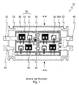
- Fig. 1 shows a power semiconductor module according to the prior art in plan view.
- a power semiconductor module consisting of a base plate (20) for mounting on a heat sink.
- this base plate (20) in the region of their corners in each case a recess (22).
- the module further consists of a frame-like housing (30) and two electrically insulating substrates (50).
- the respective substrate in turn consists of an insulating body (52) with a plurality of on its first base plate facing away from the main surface located opposite each other insulated metallic interconnect tracks (54).
- the substrate On its second main surface facing the base plate, the substrate has a planar metallization (53, 53) which is similar to the connecting paths of the first main surface.
- Fig. 2 on.
- connection tracks (54) Power semiconductor components (56) and a sensor component (58) are arranged on the connection tracks (54) and connected to them in a circuit-compatible manner by means of wire bonds (48).
- the submodule (10) has connection elements (40, 42, 44) for the load connections.
- the connecting tracks (54) of the substrates (50) are partly connected to each other and to the connecting elements (40) directly or by means of solder bridges (46).
- the Fig. 2 to 4 show side views of power semiconductor modules according to the prior art ( Fig. 2 ), according to the invention ( Fig. 3 ) as well as the side view through another power semiconductor module ( Fig. 4 ) each along a section AA (see. Fig. 1 ).
- a power semiconductor module (10) with a frame-like housing (30) in the side view.
- DCB Direct Copper Bonding
- This copper layer (54) represents the connecting tracks of the power semiconductor module.
- the components (56), as a rule power semiconductor components and sensor components, are arranged on these connecting tracks (54).
- the circuit-compliant connections are made by wire bonds (48).
- auxiliary connection elements of the respective power semiconductor module are shown. These are formed by contact springs (60), conductor tracks (72) arranged on a printed circuit board and connection pins (76).
- the lid itself is here like a frame and surrounds the circuit board at its edges without completely covering it.
- Fig. 2 shows a section along the line AA through the power semiconductor module according to the prior art according to Fig. 1 in side view.
- the base plate (20) consists of a flat copper plate, which has a convex bias of about 2mm in the longitudinal direction at a length of about 15cm.
- Fig. 3 shows a section through a power semiconductor module according to the invention produced in side view.
- the longitudinal sides of the base plate (20) are here without interruption over a portion (24 a) between the recesses ( Fig. 1 , 22) in each case by about 90 ° in the direction of the module interior, ie in the direction of the heat sink side facing away from the base plate (20), bent upwards.
- this stiffening structure (24) can be used in comparison to the prior art by at least 20% thinner base plate while increasing the bending stiffness by 60%.
- a convexly biased base plate retains this convex bias even after the substrates have been soldered.
- the bias is also here as in the prior art at about 2mm.
- Fig. 4 shows a section through a non-inventively prepared power semiconductor module in side view.
- a stiffening structure (24) of the base plate (20) is realized by longitudinally extending embossing areas (24b) are arranged in several sections along the longitudinal side of the power semiconductor module (10). These embossed areas are designed such that on the side facing the heat sink (80), the material of the base bar (20), as a rule copper, is pressed partially in the direction of the module interior. This results in a bulge on the side facing away from the heat sink (80) side of the base plate (20). As a result, stiffening in the longitudinal direction is achieved in the region of the embossing.
- the embossing areas (24b) advantageously have a length to width ratio of more than 4: 1. Furthermore, it is advantageous if the individual embossed areas overlap each other by more than 20%.
- the base plate (20) has the above-described convex bias on. Alternatively, of course, a single embossment (24b) over the entire length of the base plate (20) may be arranged extending in the longitudinal direction.
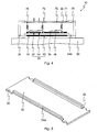
- Fig. 5 shows a base plate of a power semiconductor module according to the invention produced in three-dimensional view.
- a base plate (20, cf. Fig. 3 ) wherein between the for the screw connection of the power semiconductor module (10) with the heat sink (80) certain recesses (22) on each longitudinal side by introducing recesses (26) a portion (24a) punched free.
- the portion (24a) is bent out of the plane given by the base plate itself out in the direction of the substrate.
- the base plate (20) is convex, as described above, biased.
- the design of the base plate (20) of the power semiconductor component according to the invention is carried out in a known punching and bending technique.
Landscapes
- Engineering & Computer Science (AREA)
- Microelectronics & Electronic Packaging (AREA)
- Chemical & Material Sciences (AREA)
- Ceramic Engineering (AREA)
- Inorganic Chemistry (AREA)
- Cooling Or The Like Of Semiconductors Or Solid State Devices (AREA)
- Die Bonding (AREA)
Description
- Die Erfindung beschreibt ein Verfahren zur Herstellung eines Leistungshalbleitermoduls, welches aus einem Gehäuse mit Grundplatte und mindestens einem darin angeordneten elektrisch isolierenden Substrat besteht. Dieses Substrat besteht seinerseits aus einem Isolierstoffkörper mit einer Mehrzahl darauf befindlicher gegeneinander isolierter metallischer Verbindungsbahnen und hierauf befindlichen und mit diesen Verbindungsbahnen schaltungsgerecht verbundenen Leistungshalbleiterbauelementen. Vorteilhafterweise weist das Substrat auf seiner Unterseite eine flächige metallische Schicht, vergleichbar den Verbindungsbahnen, auf. Weiterhin weisen derartige Leistungshalbleitermodule Anschlusselemente für Last- und Hilfskontakte auf.
- Leistungshalbleitermodule, die Ausgangspunkt dieser Erfindung sind, sind beispielhaft bekannt aus
DE 103 16 355 . Derartige Leistungshalbleitermodule weisen eine Grundplatte zur thermischen Kopplung an einen Kühlkörper auf. Hierfür ist es von besonderer Bedeutung, dass die Grundplatte nach der Befestigung des Leistungshalbeitermoduls möglichst vollständig in Kontakt mit dem Kühlkörper ist um einen effizienten Wärmeübergang zu gewährleisten. Da bei modernen Leistungshalbleitermodulen besonderer Wert auf eine kompakte Bauform gelegt wird und deswegen der Flächenanteil des Substrates mit den darauf angeordneten Leistungshalbleiterbauelementen besonders hoch ist, weisen diese Leistungshalbleitermodule ausschließlich in den Eckbereichen Verbindungseinrichtungen zur Verbindung mit dem Kühlkörper auf. Besonders Leistungshalbleitermodule mit hohen Leistungen weisen vorteilhafterweise eine Bauform auf, bei der die Längsausdehnung wesentlich größer ist als die Querausdehnung. Es ist bevorzugt, dass das Substrat auf der der Grundplatte zugewandten Seite eine weitere Metallisierung aufweist. Mittels dieser Metallisierung sind die Substrate stoffschlüssig mit der Grundplatte verbunden. Nach dem Stand der Technik wird diese Verbindung mittels Löten hergestellt. - Aus der
WO03/046981 - Aus der
EP 0 144 8066 A2 - Bei Leistungshalbleitermodulen mit vergleichsweise großer Längsausdehnung kann eine Lötverbindung der Substrate und der Grundplatte zu einer konkaven Durchbiegung der Grundplatte führen. Unter konkaver Durchbiegung soll hier eine Durchbiegung verstanden werden, bei der die Durchbiegung des Mittelbereichs der Grundplatte in Richtung des Leistungshalbleitermoduls erfolgt, unter konvexer Durchbiegung wird eine Durchbiegung in Richtung des Kühlkörpers verstanden. Vorteilhaft für einen effizienten Wärmeübergang zwischen dem Leistungshalbleitermodul und dem Kühlkörper ist eine konvexe Durchbiegung der Grundplatte, da somit die Grundplatte nach der Befestigung auf dem Kühlkörper plan auf diesem aufliegt. Bei konkaver Durchbiegung würde keine plane Auflage erfolgen. Bereits bei der Herstellung werden somit die Grundplatten nach dem Stand der Technik mit einer konvexen Durchbiegung gefertigt. Trotz dieser sog. Vorspannung der Grundplatte kann die Lötung der Substrate zu einer konkaven Durchbiegung der Grundplatte führen, falls diese nicht ausreichend steif ausgeführt ist. Eine ausreichende Steifigkeit wird nach dem Stand der Technik durch eine entsprechend dicke Auslegung der Grundplatte erreicht.
- Andererseits fordert eine kostengünstige und kompakte Herstellung eines Leistungshalbleitermoduls eine Grundplatte mit möglichst geringer Dicke. Leistungshalbleitermodule, speziell mit im Vergleich zur Querausdehnung wesentlich größerer Längsausdehnung, weisen nach dem Stand der Technik somit entweder den Nachteil einer dicken Grundplatte oder der konkaven Durchbiegung einer dünneren Grundplatte auf.
- Der vorliegenden Erfindung liegt daher die Aufgabe zu Grunde ein Herstellungsverfahren für ein Leistungshalbleitermodul vorzustellen, bei dem die Biegesteifigkeit in Längsrichtung der Grundplatte bei gegebener Dicke erhöht ist.
- Diese Aufgabe wird gelöst durch ein Verfahren zur Herstellung eines Leistungshalbleitermoduls nach dem Anspruch 1, spezielle Ausgestaltungen finden sich in den Unteransprüchen.
- Der Grundgedanke der Erfindung geht aus von einem Leistungshalbleitermodul mit einer Grundplatte zur Montage auf einem Kühlkörper nach dem genannten Stand der Technik bestehend aus einem rahmenartigen Gehäuse mit mindestens einem darin angeordneten elektrisch isolierenden Substrat. Dieses Substrat besteht seinerseits aus einem Isolierstoffkörper mit einer Mehrzahl von auf seiner ersten Hauptfläche befindlichen gegeneinander isolierten metallischen Verbindungsbahnen sowie vorzugsweise aus einer auf seiner zweiten Hauptfläche angeordneten flächigen metallischen Schicht. Auf den Verbindungsbahnen der ersten Hauptfläche und mit diesen Verbindungsbahnen schaltungsgerecht verbunden ist eine Mehrzahl von Leistungshalbleiterbauelementen angeordnet. Das Leistungshalbleitermodul weist weiterhin nach außen führende Anschlusselemente für Last- und Hilfskontakte auf.
- Das erfinderische Verfahren zur Herstellung weist ein Leistungshalbleitermodul mit einer Grundplatte auf, die in Längsrichtung mindestens eine Versteifungsstruktur aufweist. Diese Versteifungsstruktur wird durch Stanzen eines Teiles der Grundplatte gebildet und ragt aus der durch die von der Grundplatte selbst definierten Ebene parallel zum Kühlkörper heraus. Auf dieser Grundplatte ist ein Substrat, vorzugsweise allerdings eine Mehrzahl einzelner Substrate, angeordnet. Vorzugsweise handelt es sich hierbei um eine stoffschlüssige Verbindung, die nach dem Stand der Technik als Lötverbindung ausgebildet ist.
- Vorteilhaft an diesem Verfahren zur Herstellung eines Leistungshalbleitermoduls ist, dass bei gegebener Dicke der Grundplatte deren Steifigkeit in Längsrichtung wesentlich erhöht ist und somit eine bei der Herstellung der Grundplatte produzierte konvexe Durchbiegung auch nach der Lötung der Substrate gegeben ist.
- Die Erfindung wird anhand von Ausführungsbeispielen in Verbindung mit den
Fig. 1 bis 5 näher erläutert. - Fig. 1
- zeigt ein Leistungshalbleitermodul nach dem Stand der Technik in Draufsicht.
- Fig. 2
- zeigt einen Schnitt entlang der Linie A-A durch das Leistungshalbleitermodul nach
Fig. 1 in Seitenansicht. - Fig. 3
- zeigt einen Schnitt durch ein erfindungsgemäßes hergestelltes Leistungshalbleitermoduls in Seitenansicht.
- Fig. 4
- zeigt einen Schnitt durch ein nicht erfindungsgemäß hergestelltes Leistungshalbleitermodul in Seitenansicht.
- Fig. 5
- zeigt eine Grundplatte eines erfindungsgemäßen Leistungshalbleitermoduls in dreidimensionaler Ansicht.
-
Fig. 1 zeigt ein Leistungshalbleitermodul nach dem Stand der Technik in Draufsicht. Dargestellt ist ein Leistungshalbleitermodul (10) bestehend aus einer Grundplatte (20) zur Montage auf einem Kühlkörper. Hierzu weist diese Grundplatte (20) im Bereich ihrer Ecken jeweils eine Ausnehmung (22) auf. Das Modul besteht weiterhin aus einem rahmenartigen Gehäuse (30) sowie zwei elektrisch isolierenden Substraten (50). Das jeweilige Substrat besteht seinerseits aus einem Isolierstoffkörper (52) mit einer Mehrzahl von auf seiner ersten der Grundplatte abgewandten Hauptfläche befindlichen gegeneinander isolierten metallischen Verbindungsbahnen (54). Auf seiner zweiten der Grundplatte zugewandten Hauptfläche weist das Substrat eine den Verbindungsbahnen der ersten Hauptfläche gleichartige flächige Metallisierung (53,Fig. 2 ) auf. Auf den Verbindungsbahnen (54) und mit diesen schaltungsgerecht mittels Drahtbondverbindungen (48) verbunden sind Leistungshalbleiterbauelemente (56) sowie ein Sensorikbauteil (58) angeordnet. Zur elektrischen Kontaktierung weist das Teilmodul (10) Anschlusselemente (40, 42, 44) für die Lastanschlüsse auf. Die Verbindungsbahnen (54) der Substrate (50) sind zum Teil miteinander und mit den Anschlusselementen (40) direkt oder mittels Lötbrücken (46) miteinander verbunden. - Die
Fig. 2 bis 4 zeigen Seitenansichten durch Leistungshalbleitermodule nach dem Stand der Technik (Fig. 2 ), gemäß der Erfindung (Fig. 3 ) sowie die Seitenansicht durch ein anderes Leistungs halbleitermodule (Fig. 4 ) jeweils entlang eines Schnittes A-A (vgl.Fig. 1 ). Dargestellt ist jeweils ein Leistungshalbleitermodul (10) mit einem rahmenartigen Gehäuse (30) in der Seitenansicht. Auf der Grundplatte (20) angeordnet ist ein sog. DCB- (Direct Copper Bonding) Substrat (50). Dieses besteht aus einem Isolierstoffkörper (52), beispielhaft einer Aluminiumoxid- oder Aluminiumnitridkeramik, mit einer auf seiner der Grundplatte zugewandten Seite flächigen (53) und auf seiner der Grundplatte (20) abgewandten Seite strukturierten Kupferschicht (54). Diese Kupferschicht (54) stellt die Verbindungsbahnen des Leistungshalbleitermoduls dar. Auf diesen Verbindungsbahnen (54) sind die Bauelemente (56), in der Regel Leistungshalbleiterbauelemente und Sensorikbauteile, angeordnet. Die schaltungsgerechten Verbindungen erfolgen mittels Drahtbondverbindungen (48). - Weiterhin sind die Hilfsanschlusselemente des jeweiligen Leistungshalbleitermoduls dargestellt. Diese werden gebildet durch Kontaktfedern (60), auf einer Leiterplatte angeordnete Leiterbahnen (72) sowie Anschlussstifte (76). Die Leiterplatte, auf deren Kontaktflächen (78) diese Kontaktfedern enden, ist hier integraler Bestandteil des Deckels (70). Der Deckel selbst ist hier rahmenartig ausgebildet und umschließt die Leiterplatte an ihren Kanten, ohne sie vollständig zu überdecken.
-
Fig. 2 zeigt einen Schnitt entlang der Linie A-A durch das Leistungshalbleitermodul nach dem Stand der Technik gemäßFig. 1 in Seitenansicht. Die Grundplatte (20) besteht aus einer ebene Kupferplatte, die in Längsrichtung eine konvexe Vorspannung von ca. 2mm bei einer Länge von ca. 15cm aufweist. -
Fig. 3 zeigt einen Schnitt durch ein erfindungsgemäß hergestelltes Leistungshalbleitermodul in Seitenansicht. Die Längsseiten der Grundplatte (20) sind hier ohne Unterbrechung über einen Abschnitt (24a) zwischen den Ausnehmungen (Fig. 1 , 22) jeweils um ca. 90° in Richtung des Modulinneren, also in Richtung der dem Kühlkörper abgewandten Seite der Grundplatte (20), nach oben gebogen. Durch diese Versteifungsstruktur (24) kann eine im Vergleich zum Stand der Technik um mindestens 20% dünnere Grundplatte eingesetzt werden bei gleichzeitiger Erhöhung der Biegesteifigkeit um 60%. Eine konvex vorgespannte Grundplatte behält auch nach der Lötung der Substrate diese konvexe Vorspannung. Die Vorspannung liegt hier ebenfalls wie beim Stand der Technik bei ca. 2mm. -
Fig. 4 . zeigt einen Schnitt durch ein nicht erfindungsgemäß hergestelltes Leistungshalbleitermodul in Seitenansicht. Hierbei wird eine Versteifungsstruktur (24) der Grundplatte (20) realisiert, indem in mehreren Abschnitten entlang der Längsseite des Leistungshalbleitermoduls (10) in Längsrichtung verlaufende Prägebereiche (24b) angeordnet sind. Diese Prägebereiche sind derart gestaltet, dass auf der dem Kühlkörper (80) zugewandten Seite das Material der Grundlatte (20), in der Regel Kupfer, partiell in Richtung des Modulinneren gedrückt wird. Hierdurch ergibt sich auf der dem Kühlkörper (80) abgewandten Seite der Grundplatte (20) eine Aufwölbung. Hierdurch wird in dem Bereich der Prägung eine Versteifung in Längsrichtung erreicht. Die Prägebereiche (24b) weisen vorteilhafterweise ein Verhältnis Länge zu Breite von mehr als 4:1 auf. Weiterhin ist es vorteilhaft, wenn die einzelnen Prägebereiche sich gegenseitig zu mehr als 20% überlappen. Zusätzlich weist die Grundplatte (20) die oben beschriebene konvexe Vorspannung auf. Alternativ kann selbstverständlich auch eine einzige Prägung (24b) über die gesamte Länge der Grundplatte (20) in Längsrichtung verlaufend angeordnet sein. -
Fig. 5 zeigt eine Grundplatte eines erfindungsgemäß hergestellten Leistungshalbleitermoduls in dreidimensionaler Ansicht. Hier ist eine Grundplatte (20, vgl.Fig. 3 )) gezeigt, wobei zwischen den für die Schraubverbindung des Leistungshalbleitermoduls (10) mit dem Kühlkörper (80) bestimmten Ausnehmungen (22) an jeder Längsseite durch Einbringen von Aussparungen (26) ein Abschnitt (24a) frei gestanzt. Der Abschnitt (24a) ist aus der durch die Grundplatte selbst gegebenen Ebene heraus in Richtung des Substrates gebogen. Weiterhin ist die Grundplatte (20) konvex, wie oben beschrieben, vorgespannt. Die Ausgestaltung der Grundplatte (20) des erfindungsgemäßen hergestellten Leistungshalbleiterbauelements erfolgt in bekannter Stanz- Biege- Technik.
Claims (6)
- Verfahren zur Herstellung eines Leistungshalbleitermoduls (10),
wobei das Leistungshalbleitermodul (10) besteht aus einer metallischen Grundplatte (20) zur Montage auf einem Kühlkörper (80), einem rahmenartigen Gehäuse (30), einem Deckel (70), nach außen führenden Anschlusselementen für Last- (40, 42, 44) und Hilfskontakte (76) und mindestens einem innerhalb des Gehäuses (30) angeordneten elektrisch isolierenden Substrat (50), das seinerseits besteht aus einem Isolierstoffkörper (52) und einer auf dessen der Grundplatte (20) abgewandten ersten Hauptfläche befindlichen Mehrzahl von gegeneinander elektrisch isolierten metallischen Verbindungsbahnen (54), darauf befindlichen und mit diesen Verbindungsbahnen schaltungsgerecht verbundenen Leistungshalbleiterbauelementen (56) sowie mindestens einer auf dessen der Grundplatte (20) zugewandten zweiten Hauptfläche befindlichen metallischen Schicht (53), wobei das Substrat (50) auf der Grundplatte (20) angeordnet ist und wobei die Grundplatte (20) eine Versteifungsstruktur (24) aufweist, die in Längsrichtung der Grundplatte (20) verläuft,
wobei diese Versteifungsstruktur (24) aus dem Grundplattenmaterial selbst gebildet ist und aus der durch die Grundplatte gegebenen Ebene herausragt, wobei die Versteifungsstruktur (24) aus Abschnitten (24a) der Längsseiten der Grundplatte (20) hergestellt wird, die aus der durch die Grundplatte selbst gegebenen Ebene heraus in Richtung des Substrates (50) gebogen werden,
wobei die Grundplatte (20) als Stanz- Biege- Teil hergestellt wird, und wobei die Abschnitte (24a) zur Versteifung durch Einbringen von Aussparungen (26) frei gestanzt werden. - Verfahren zur Herstellung eines Leistungshalbleitermoduls (10) nach Anspruch 1, wobei die Grundplatte (20) eine Mehrzahl von Ausnehmungen (22) zur Schraubverbindung des Leistungshalbleitermoduls mit dem Kühlkörper (80) aufweist.
- Verfahren zur Herstellung eines Leistungshalbleitermoduls (10) nach Anspruch 1, wobei die Grundplatte (20) mit der metallischen Schicht (53) des Substrats (50) mittels einer flächig ausgeführten Lötung stoffbündig verbundene wird.
- Verfahren zur Herstellung eines Leistungshalbleitermoduls (10) nach Anspruch 1, wobei die Abschnitte (24a) jeder Seite unterbrochen angeordnet sind.
- Verfahren zur Herstellung eines Leistungshalbleitermoduls (10) nach Anspruch 1, wobei der jeweilige Abschnitt (24a) zur Versteifung zwischen Ausnehmungen (22) der Grundplatte (20) für Schraubverbindungen angeordnet und von diesen beabstandet ist.
- Verfahren zur Herstellung eines Leistungshalbleitermoduls (10) nach Anspruch 1, wobei die Abschnitte (24a) im rechten Winkel zur Grundplatte (20) in dem Kühlkörper (80) abgewandter Richtung gebogen werden.
Applications Claiming Priority (2)
| Application Number | Priority Date | Filing Date | Title |
|---|---|---|---|
| DE10333329A DE10333329B4 (de) | 2003-07-23 | 2003-07-23 | Leistungshalbleitermodul mit biegesteifer Grundplatte |
| DE10333329 | 2003-07-23 |
Publications (3)
| Publication Number | Publication Date |
|---|---|
| EP1501127A2 EP1501127A2 (de) | 2005-01-26 |
| EP1501127A3 EP1501127A3 (de) | 2007-10-24 |
| EP1501127B1 true EP1501127B1 (de) | 2009-06-24 |
Family
ID=33483017
Family Applications (1)
| Application Number | Title | Priority Date | Filing Date |
|---|---|---|---|
| EP04014433A Expired - Lifetime EP1501127B1 (de) | 2003-07-23 | 2004-06-19 | Verfahren zur Herstellung eines Leistungshalbleitermoduls mit biegesteifer Grundplatte |
Country Status (6)
| Country | Link |
|---|---|
| US (1) | US7030491B2 (de) |
| EP (1) | EP1501127B1 (de) |
| JP (1) | JP4264392B2 (de) |
| KR (1) | KR100990527B1 (de) |
| AT (1) | ATE434833T1 (de) |
| DE (2) | DE10333329B4 (de) |
Cited By (1)
| Publication number | Priority date | Publication date | Assignee | Title |
|---|---|---|---|---|
| US9929066B1 (en) | 2016-12-13 | 2018-03-27 | Ixys Corporation | Power semiconductor device module baseplate having peripheral heels |
Families Citing this family (14)
| Publication number | Priority date | Publication date | Assignee | Title |
|---|---|---|---|---|
| DE102005063532B3 (de) | 2005-02-17 | 2022-03-10 | Infineon Technologies Ag | Leistungshalbleiterbaugruppe |
| DE102005007373B4 (de) | 2005-02-17 | 2013-05-29 | Infineon Technologies Ag | Leistungshalbleiterbaugruppe |
| JP2006253183A (ja) * | 2005-03-08 | 2006-09-21 | Hitachi Ltd | 半導体パワーモジュール |
| DE102005037522A1 (de) * | 2005-08-09 | 2007-02-15 | Semikron Elektronik Gmbh & Co. Kg | Leistungshalbleitermodul mit wannenförmigem Grundkörper |
| DE102005039278A1 (de) | 2005-08-19 | 2007-02-22 | Semikron Elektronik Gmbh & Co. Kg | Leistungshalbleitermodul mit Leitungselement |
| DE102006058692A1 (de) * | 2006-12-13 | 2008-06-26 | Semikron Elektronik Gmbh & Co. Kg | Leistungshalbleitermodul mit Kontaktfedern |
| DE102007010883A1 (de) * | 2007-03-06 | 2008-09-18 | Infineon Technologies Ag | Leistungshalbleiteranordnung und Verfahren zu dessen Herstellung |
| DE102007036566A1 (de) * | 2007-08-03 | 2009-02-19 | Siemens Ag | Federkontaktierung von elektrischen Kontaktflächen eines elektronischen Bauteils |
| DE102008054932B4 (de) * | 2008-12-18 | 2011-12-01 | Infineon Technologies Ag | Leistungshalbleitermodul mit versteifter Bodenplatte |
| DE102009035819A1 (de) | 2009-08-01 | 2011-02-03 | Semikron Elektronik Gmbh & Co. Kg | Leistungshalbleitermodul mit stromsymmetrischem Lastanschlusselement |
| JP5512377B2 (ja) | 2010-04-28 | 2014-06-04 | 本田技研工業株式会社 | 回路基板 |
| EP3573096B1 (de) | 2011-06-27 | 2022-03-16 | Rohm Co., Ltd. | Halbleitermodul |
| WO2020245890A1 (ja) * | 2019-06-03 | 2020-12-10 | 三菱電機株式会社 | パワーモジュール及び電力変換装置 |
| US20240063080A1 (en) * | 2022-04-28 | 2024-02-22 | Hitachi Energy Switzerland Ag | Semiconductor power module and method for manufacturing a semiconductor power module |
Family Cites Families (15)
| Publication number | Priority date | Publication date | Assignee | Title |
|---|---|---|---|---|
| JPS60113931A (ja) * | 1983-11-25 | 1985-06-20 | Toshiba Corp | 半導体装置 |
| JPS60216572A (ja) * | 1984-04-11 | 1985-10-30 | Sanyo Electric Co Ltd | ヒ−トシンクの製造方法 |
| DE3508456C2 (de) * | 1985-03-09 | 1987-01-08 | Brown, Boveri & Cie Ag, 6800 Mannheim | Leistungshalbleitermodul und Verfahren zur Herstellung eines solchen Moduls |
| EP0400177A1 (de) * | 1989-05-31 | 1990-12-05 | Siemens Aktiengesellschaft | Verbindung eines Halbleiterbauelements mit einem Metallträger |
| JPH09172116A (ja) * | 1995-12-21 | 1997-06-30 | Mitsubishi Electric Corp | 半導体装置 |
| DE19707514C2 (de) * | 1997-02-25 | 2002-09-26 | Eupec Gmbh & Co Kg | Halbleitermodul |
| JP2000196175A (ja) * | 1998-12-28 | 2000-07-14 | Toshiba Corp | サブキャリア及び半導体装置 |
| JP2000307058A (ja) * | 1999-04-19 | 2000-11-02 | Mitsubishi Electric Corp | パワー半導体モジュール |
| WO2001008219A1 (de) * | 1999-07-23 | 2001-02-01 | eupec Europäische Gesellschaft für Leistungshalbleiter mbH & Co. KG | Halbleitermodul |
| JP4044265B2 (ja) * | 2000-05-16 | 2008-02-06 | 三菱電機株式会社 | パワーモジュール |
| US6697399B2 (en) * | 2000-05-26 | 2004-02-24 | The Furukawa Electric Co., Ltd. | Semiconductor laser module with peltier module for regulating a temperature of a semiconductor laser chip |
| DE10064979C1 (de) * | 2000-12-18 | 2002-02-28 | Dieter Loewer | Schaltungsanordnung und Verfahren zur Herstellung einer solchen Anordnung |
| JP2003158229A (ja) | 2001-11-21 | 2003-05-30 | Mitsubishi Electric Corp | パワー半導体モジュールの製造装置 |
| JP2003163315A (ja) * | 2001-11-29 | 2003-06-06 | Denki Kagaku Kogyo Kk | モジュール |
| DE10316355C5 (de) | 2003-04-10 | 2008-03-06 | Semikron Elektronik Gmbh & Co. Kg | Leistungshalbeitermodul mit flexibler äusserer Anschlussbelegung |
-
2003
- 2003-07-23 DE DE10333329A patent/DE10333329B4/de not_active Expired - Lifetime
-
2004
- 2004-06-19 DE DE502004009640T patent/DE502004009640D1/de not_active Expired - Lifetime
- 2004-06-19 AT AT04014433T patent/ATE434833T1/de not_active IP Right Cessation
- 2004-06-19 EP EP04014433A patent/EP1501127B1/de not_active Expired - Lifetime
- 2004-07-12 JP JP2004204701A patent/JP4264392B2/ja not_active Expired - Lifetime
- 2004-07-21 KR KR1020040056936A patent/KR100990527B1/ko not_active Expired - Lifetime
- 2004-07-23 US US10/897,719 patent/US7030491B2/en not_active Expired - Lifetime
Cited By (1)
| Publication number | Priority date | Publication date | Assignee | Title |
|---|---|---|---|---|
| US9929066B1 (en) | 2016-12-13 | 2018-03-27 | Ixys Corporation | Power semiconductor device module baseplate having peripheral heels |
Also Published As
| Publication number | Publication date |
|---|---|
| KR100990527B1 (ko) | 2010-10-29 |
| DE10333329A1 (de) | 2005-03-10 |
| DE502004009640D1 (de) | 2009-08-06 |
| ATE434833T1 (de) | 2009-07-15 |
| KR20050011714A (ko) | 2005-01-29 |
| JP2005045238A (ja) | 2005-02-17 |
| EP1501127A2 (de) | 2005-01-26 |
| DE10333329B4 (de) | 2011-07-21 |
| EP1501127A3 (de) | 2007-10-24 |
| US20050035445A1 (en) | 2005-02-17 |
| JP4264392B2 (ja) | 2009-05-13 |
| US7030491B2 (en) | 2006-04-18 |
Similar Documents
| Publication | Publication Date | Title |
|---|---|---|
| EP1713124B1 (de) | Leistungshalbleitermodul mit Verbindungsbahnen und mit Anschlusselementen, die mit den Verbindungsbahnen verbunden sind | |
| EP1501127B1 (de) | Verfahren zur Herstellung eines Leistungshalbleitermoduls mit biegesteifer Grundplatte | |
| EP1450404B1 (de) | Anordnung in Druckkontaktierung mit einem Leistungshalbleitermodul | |
| DE19928788B4 (de) | Elektronisches Keramikbauelement | |
| DE10033977B4 (de) | Zwischenverbindungsstruktur zum Einsatz von Halbleiterchips auf Schichtträgern | |
| EP1592063B1 (de) | Anordnung in Druckkontaktierung mit einem Leistungshalbleitermodul | |
| DE102005049687B4 (de) | Leistungshalbleiterbauteil in Flachleitertechnik mit vertikalem Strompfad und Verfahren zur Herstellung | |
| EP1841299A2 (de) | Verbindungseinrichtung für elektronishche Bauelemente | |
| WO2013013964A1 (de) | Trägervorrichtung, elektrische vorrichtung mit einer trägervorrichtung und verfahren zur herstellung dieser | |
| DE102006015447B4 (de) | Leistungshalbleiterbauelement mit einem Leistungshalbleiterchip und Verfahren zur Herstellung desselben | |
| EP1169736B1 (de) | Leistungshalbleitermodul | |
| DE102006014582B4 (de) | Halbleitermodul | |
| DE10227658A1 (de) | Metall-Keramik-Substrat für elektrische Schaltkreise -oder Module, Verfahren zum Herstellen eines solchen Substrates sowie Modul mit einem solchen Substrat | |
| DE10337640A1 (de) | Leistungshalbleitermodul mit verbessertem thermischen Kontakt | |
| DE102005047567B3 (de) | Leistungshalbleitermodul mit Isolationszwischenlage und Verfahren zu seiner Herstellung | |
| DE102021121875B4 (de) | Halbleitereinrichtung und herstellungsverfahren einer halbleitereinrichtung | |
| EP3770959A1 (de) | Verbindungsmethode für leistungsmodule mit einer zwischenkreisverschienung | |
| DE102005030247B4 (de) | Leistungshalbleitermodul mit Verbindungselementen hoher Stromtragfähigkeit | |
| DE102005050534A1 (de) | Leistungshalbleitermodul | |
| WO2019042653A1 (de) | Schaltungsträger für leistungselektronik und leistungselektronikmodul mit einem schaltungsträger | |
| DE102009044933B4 (de) | Leistungshalbleitermodul mit mindestens zwei verbundenen Schaltungsträgern und Verfahren zur Herstellung eines Leistungshalbleitermoduls mit mindestens zwei verbundenen Schaltungsträgern | |
| DE102006058695B4 (de) | Leistungshalbleitermodul mit stumpf gelötetem Anschlusselement | |
| WO2007045112A1 (de) | Leistungsgehäuse für halbleiterchips und deren anordnung zur wärmeabfuhr | |
| DE19931694B4 (de) | Verfahren zum Herstellen von elektrischen Schaltkreisen oder Modulen sowie elektrischer Schaltkreis oder elektrisches Modul hergestellt nach diesem Verfahren | |
| DE102007002807A1 (de) | Chipanordnung und Verfahren zur Herstellung einer Chipanordnung |
Legal Events
| Date | Code | Title | Description |
|---|---|---|---|
| PUAI | Public reference made under article 153(3) epc to a published international application that has entered the european phase |
Free format text: ORIGINAL CODE: 0009012 |
|
| AK | Designated contracting states |
Kind code of ref document: A2 Designated state(s): AT BE BG CH CY CZ DE DK EE ES FI FR GB GR HU IE IT LI LU MC NL PL PT RO SE SI SK TR |
|
| AX | Request for extension of the european patent |
Extension state: AL HR LT LV MK |
|
| RAP1 | Party data changed (applicant data changed or rights of an application transferred) |
Owner name: SEMIKRON ELEKTRONIK GMBH & CO. KG |
|
| PUAL | Search report despatched |
Free format text: ORIGINAL CODE: 0009013 |
|
| AK | Designated contracting states |
Kind code of ref document: A3 Designated state(s): AT BE BG CH CY CZ DE DK EE ES FI FR GB GR HU IE IT LI LU MC NL PL PT RO SE SI SK TR |
|
| AX | Request for extension of the european patent |
Extension state: AL HR LT LV MK |
|
| RIC1 | Information provided on ipc code assigned before grant |
Ipc: H01L 23/492 20060101ALI20070918BHEP Ipc: H01L 21/48 20060101ALI20070918BHEP Ipc: H01L 23/373 20060101ALI20070918BHEP Ipc: H01L 25/07 20060101AFI20041115BHEP |
|
| 17P | Request for examination filed |
Effective date: 20071012 |
|
| 17Q | First examination report despatched |
Effective date: 20071213 |
|
| AKX | Designation fees paid |
Designated state(s): AT BE BG CH CY CZ DE DK EE ES FI FR GB GR HU IE IT LI LU MC NL PL PT RO SE SI SK TR |
|
| RTI1 | Title (correction) |
Free format text: METHOD OF MANUFACTURING A POWER SEMICONDUCTOR MODULE WITH A BASE PLATE HAVING HIGH BENDING STIFFNESS |
|
| GRAP | Despatch of communication of intention to grant a patent |
Free format text: ORIGINAL CODE: EPIDOSNIGR1 |
|
| GRAS | Grant fee paid |
Free format text: ORIGINAL CODE: EPIDOSNIGR3 |
|
| GRAA | (expected) grant |
Free format text: ORIGINAL CODE: 0009210 |
|
| REG | Reference to a national code |
Ref country code: DE Ref legal event code: R081 Ref document number: 502004009640 Country of ref document: DE Owner name: SEMIKRON ELEKTRONIK GMBH & CO. KG, DE Free format text: FORMER OWNER: SEMIKRON ELEKTRONIK GMBH, 90431 NUERNBERG, DE |
|
| AK | Designated contracting states |
Kind code of ref document: B1 Designated state(s): AT BE BG CH CY CZ DE DK EE ES FI FR GB GR HU IE IT LI LU MC NL PL PT RO SE SI SK TR |
|
| REG | Reference to a national code |
Ref country code: GB Ref legal event code: FG4D Free format text: NOT ENGLISH |
|
| REG | Reference to a national code |
Ref country code: CH Ref legal event code: EP |
|
| REG | Reference to a national code |
Ref country code: IE Ref legal event code: FG4D Free format text: LANGUAGE OF EP DOCUMENT: GERMAN |
|
| REF | Corresponds to: |
Ref document number: 502004009640 Country of ref document: DE Date of ref document: 20090806 Kind code of ref document: P |
|
| REG | Reference to a national code |
Ref country code: DE Ref legal event code: R096 Ref document number: 502004009640 Country of ref document: DE Effective date: 20090806 |
|
| REG | Reference to a national code |
Ref country code: CH Ref legal event code: NV Representative=s name: BRAUNPAT BRAUN EDER AG |
|
| PG25 | Lapsed in a contracting state [announced via postgrant information from national office to epo] |
Ref country code: FI Free format text: LAPSE BECAUSE OF FAILURE TO SUBMIT A TRANSLATION OF THE DESCRIPTION OR TO PAY THE FEE WITHIN THE PRESCRIBED TIME-LIMIT Effective date: 20090624 |
|
| PG25 | Lapsed in a contracting state [announced via postgrant information from national office to epo] |
Ref country code: SE Free format text: LAPSE BECAUSE OF FAILURE TO SUBMIT A TRANSLATION OF THE DESCRIPTION OR TO PAY THE FEE WITHIN THE PRESCRIBED TIME-LIMIT Effective date: 20090924 Ref country code: PL Free format text: LAPSE BECAUSE OF FAILURE TO SUBMIT A TRANSLATION OF THE DESCRIPTION OR TO PAY THE FEE WITHIN THE PRESCRIBED TIME-LIMIT Effective date: 20090624 Ref country code: SI Free format text: LAPSE BECAUSE OF FAILURE TO SUBMIT A TRANSLATION OF THE DESCRIPTION OR TO PAY THE FEE WITHIN THE PRESCRIBED TIME-LIMIT Effective date: 20090624 |
|
| NLV1 | Nl: lapsed or annulled due to failure to fulfill the requirements of art. 29p and 29m of the patents act | ||
| PG25 | Lapsed in a contracting state [announced via postgrant information from national office to epo] |
Ref country code: EE Free format text: LAPSE BECAUSE OF FAILURE TO SUBMIT A TRANSLATION OF THE DESCRIPTION OR TO PAY THE FEE WITHIN THE PRESCRIBED TIME-LIMIT Effective date: 20090624 Ref country code: ES Free format text: LAPSE BECAUSE OF FAILURE TO SUBMIT A TRANSLATION OF THE DESCRIPTION OR TO PAY THE FEE WITHIN THE PRESCRIBED TIME-LIMIT Effective date: 20091005 Ref country code: CZ Free format text: LAPSE BECAUSE OF FAILURE TO SUBMIT A TRANSLATION OF THE DESCRIPTION OR TO PAY THE FEE WITHIN THE PRESCRIBED TIME-LIMIT Effective date: 20090624 |
|
| REG | Reference to a national code |
Ref country code: IE Ref legal event code: FD4D |
|
| PG25 | Lapsed in a contracting state [announced via postgrant information from national office to epo] |
Ref country code: NL Free format text: LAPSE BECAUSE OF FAILURE TO SUBMIT A TRANSLATION OF THE DESCRIPTION OR TO PAY THE FEE WITHIN THE PRESCRIBED TIME-LIMIT Effective date: 20090624 |
|
| PG25 | Lapsed in a contracting state [announced via postgrant information from national office to epo] |
Ref country code: BG Free format text: LAPSE BECAUSE OF FAILURE TO SUBMIT A TRANSLATION OF THE DESCRIPTION OR TO PAY THE FEE WITHIN THE PRESCRIBED TIME-LIMIT Effective date: 20090924 Ref country code: PT Free format text: LAPSE BECAUSE OF FAILURE TO SUBMIT A TRANSLATION OF THE DESCRIPTION OR TO PAY THE FEE WITHIN THE PRESCRIBED TIME-LIMIT Effective date: 20091024 |
|
| PG25 | Lapsed in a contracting state [announced via postgrant information from national office to epo] |
Ref country code: IE Free format text: LAPSE BECAUSE OF FAILURE TO SUBMIT A TRANSLATION OF THE DESCRIPTION OR TO PAY THE FEE WITHIN THE PRESCRIBED TIME-LIMIT Effective date: 20090624 Ref country code: DK Free format text: LAPSE BECAUSE OF FAILURE TO SUBMIT A TRANSLATION OF THE DESCRIPTION OR TO PAY THE FEE WITHIN THE PRESCRIBED TIME-LIMIT Effective date: 20090624 |
|
| PLBE | No opposition filed within time limit |
Free format text: ORIGINAL CODE: 0009261 |
|
| STAA | Information on the status of an ep patent application or granted ep patent |
Free format text: STATUS: NO OPPOSITION FILED WITHIN TIME LIMIT |
|
| 26N | No opposition filed |
Effective date: 20100325 |
|
| REG | Reference to a national code |
Ref country code: DE Ref legal event code: R097 Ref document number: 502004009640 Country of ref document: DE Effective date: 20100324 |
|
| PG25 | Lapsed in a contracting state [announced via postgrant information from national office to epo] |
Ref country code: GR Free format text: LAPSE BECAUSE OF FAILURE TO SUBMIT A TRANSLATION OF THE DESCRIPTION OR TO PAY THE FEE WITHIN THE PRESCRIBED TIME-LIMIT Effective date: 20090925 |
|
| BERE | Be: lapsed |
Owner name: SEMIKRON ELEKTRONIK G.M.B.H. & CO. KG Effective date: 20100630 |
|
| PG25 | Lapsed in a contracting state [announced via postgrant information from national office to epo] |
Ref country code: MC Free format text: LAPSE BECAUSE OF NON-PAYMENT OF DUE FEES Effective date: 20100630 |
|
| PG25 | Lapsed in a contracting state [announced via postgrant information from national office to epo] |
Ref country code: BE Free format text: LAPSE BECAUSE OF NON-PAYMENT OF DUE FEES Effective date: 20100630 |
|
| PG25 | Lapsed in a contracting state [announced via postgrant information from national office to epo] |
Ref country code: AT Free format text: LAPSE BECAUSE OF NON-PAYMENT OF DUE FEES Effective date: 20100619 |
|
| PG25 | Lapsed in a contracting state [announced via postgrant information from national office to epo] |
Ref country code: CY Free format text: LAPSE BECAUSE OF FAILURE TO SUBMIT A TRANSLATION OF THE DESCRIPTION OR TO PAY THE FEE WITHIN THE PRESCRIBED TIME-LIMIT Effective date: 20090624 |
|
| PG25 | Lapsed in a contracting state [announced via postgrant information from national office to epo] |
Ref country code: LU Free format text: LAPSE BECAUSE OF NON-PAYMENT OF DUE FEES Effective date: 20100619 Ref country code: HU Free format text: LAPSE BECAUSE OF FAILURE TO SUBMIT A TRANSLATION OF THE DESCRIPTION OR TO PAY THE FEE WITHIN THE PRESCRIBED TIME-LIMIT Effective date: 20091225 |
|
| PG25 | Lapsed in a contracting state [announced via postgrant information from national office to epo] |
Ref country code: TR Free format text: LAPSE BECAUSE OF FAILURE TO SUBMIT A TRANSLATION OF THE DESCRIPTION OR TO PAY THE FEE WITHIN THE PRESCRIBED TIME-LIMIT Effective date: 20090624 |
|
| PG25 | Lapsed in a contracting state [announced via postgrant information from national office to epo] |
Ref country code: RO Free format text: LAPSE BECAUSE OF FAILURE TO SUBMIT A TRANSLATION OF THE DESCRIPTION OR TO PAY THE FEE WITHIN THE PRESCRIBED TIME-LIMIT Effective date: 20090624 |
|
| REG | Reference to a national code |
Ref country code: FR Ref legal event code: PLFP Year of fee payment: 13 |
|
| REG | Reference to a national code |
Ref country code: FR Ref legal event code: PLFP Year of fee payment: 14 |
|
| PGFP | Annual fee paid to national office [announced via postgrant information from national office to epo] |
Ref country code: SK Payment date: 20170817 Year of fee payment: 14 |
|
| REG | Reference to a national code |
Ref country code: CH Ref legal event code: PCAR Free format text: NEW ADDRESS: HOLEESTRASSE 87, 4054 BASEL (CH) |
|
| REG | Reference to a national code |
Ref country code: FR Ref legal event code: PLFP Year of fee payment: 15 |
|
| REG | Reference to a national code |
Ref country code: SK Ref legal event code: MM4A Ref document number: E 6035 Country of ref document: SK Effective date: 20180619 |
|
| PG25 | Lapsed in a contracting state [announced via postgrant information from national office to epo] |
Ref country code: SK Free format text: LAPSE BECAUSE OF NON-PAYMENT OF DUE FEES Effective date: 20180619 |
|
| PGFP | Annual fee paid to national office [announced via postgrant information from national office to epo] |
Ref country code: FR Payment date: 20230621 Year of fee payment: 20 Ref country code: DE Payment date: 20230630 Year of fee payment: 20 |
|
| PGFP | Annual fee paid to national office [announced via postgrant information from national office to epo] |
Ref country code: IT Payment date: 20230630 Year of fee payment: 20 Ref country code: GB Payment date: 20230622 Year of fee payment: 20 Ref country code: CH Payment date: 20230702 Year of fee payment: 20 |
|
| REG | Reference to a national code |
Ref country code: DE Ref legal event code: R071 Ref document number: 502004009640 Country of ref document: DE |
|
| REG | Reference to a national code |
Ref country code: CH Ref legal event code: PL |
|
| PG25 | Lapsed in a contracting state [announced via postgrant information from national office to epo] |
Ref country code: GB Free format text: LAPSE BECAUSE OF EXPIRATION OF PROTECTION Effective date: 20240618 |
|
| PG25 | Lapsed in a contracting state [announced via postgrant information from national office to epo] |
Ref country code: GB Free format text: LAPSE BECAUSE OF EXPIRATION OF PROTECTION Effective date: 20240618 |
|
| REG | Reference to a national code |
Ref country code: DE Ref legal event code: R081 Ref document number: 502004009640 Country of ref document: DE Owner name: SEMIKRON DANFOSS ELEKTRONIK GMBH & CO. KG, DE Free format text: FORMER OWNER: SEMIKRON ELEKTRONIK GMBH & CO. KG, 90431 NUERNBERG, DE |