EP1403921A2 - Dispositif electronique avec des puces semi-conductrices empilées et procédé de fabrication associée - Google Patents
Dispositif electronique avec des puces semi-conductrices empilées et procédé de fabrication associée Download PDFInfo
- Publication number
- EP1403921A2 EP1403921A2 EP03017506A EP03017506A EP1403921A2 EP 1403921 A2 EP1403921 A2 EP 1403921A2 EP 03017506 A EP03017506 A EP 03017506A EP 03017506 A EP03017506 A EP 03017506A EP 1403921 A2 EP1403921 A2 EP 1403921A2
- Authority
- EP
- European Patent Office
- Prior art keywords
- electronic component
- rewiring
- bond
- areas
- external contact
- Prior art date
- Legal status (The legal status is an assumption and is not a legal conclusion. Google has not performed a legal analysis and makes no representation as to the accuracy of the status listed.)
- Withdrawn
Links
Images


Classifications
-
- H—ELECTRICITY
- H01—ELECTRIC ELEMENTS
- H01L—SEMICONDUCTOR DEVICES NOT COVERED BY CLASS H10
- H01L25/00—Assemblies consisting of a plurality of individual semiconductor or other solid state devices ; Multistep manufacturing processes thereof
- H01L25/03—Assemblies consisting of a plurality of individual semiconductor or other solid state devices ; Multistep manufacturing processes thereof all the devices being of a type provided for in the same subgroup of groups H01L27/00 - H01L33/00, or in a single subclass of H10K, H10N, e.g. assemblies of rectifier diodes
- H01L25/04—Assemblies consisting of a plurality of individual semiconductor or other solid state devices ; Multistep manufacturing processes thereof all the devices being of a type provided for in the same subgroup of groups H01L27/00 - H01L33/00, or in a single subclass of H10K, H10N, e.g. assemblies of rectifier diodes the devices not having separate containers
- H01L25/065—Assemblies consisting of a plurality of individual semiconductor or other solid state devices ; Multistep manufacturing processes thereof all the devices being of a type provided for in the same subgroup of groups H01L27/00 - H01L33/00, or in a single subclass of H10K, H10N, e.g. assemblies of rectifier diodes the devices not having separate containers the devices being of a type provided for in group H01L27/00
- H01L25/0657—Stacked arrangements of devices
-
- H—ELECTRICITY
- H01—ELECTRIC ELEMENTS
- H01L—SEMICONDUCTOR DEVICES NOT COVERED BY CLASS H10
- H01L2224/00—Indexing scheme for arrangements for connecting or disconnecting semiconductor or solid-state bodies and methods related thereto as covered by H01L24/00
- H01L2224/01—Means for bonding being attached to, or being formed on, the surface to be connected, e.g. chip-to-package, die-attach, "first-level" interconnects; Manufacturing methods related thereto
- H01L2224/02—Bonding areas; Manufacturing methods related thereto
- H01L2224/04—Structure, shape, material or disposition of the bonding areas prior to the connecting process
- H01L2224/05—Structure, shape, material or disposition of the bonding areas prior to the connecting process of an individual bonding area
- H01L2224/0554—External layer
- H01L2224/05573—Single external layer
-
- H—ELECTRICITY
- H01—ELECTRIC ELEMENTS
- H01L—SEMICONDUCTOR DEVICES NOT COVERED BY CLASS H10
- H01L2224/00—Indexing scheme for arrangements for connecting or disconnecting semiconductor or solid-state bodies and methods related thereto as covered by H01L24/00
- H01L2224/01—Means for bonding being attached to, or being formed on, the surface to be connected, e.g. chip-to-package, die-attach, "first-level" interconnects; Manufacturing methods related thereto
- H01L2224/10—Bump connectors; Manufacturing methods related thereto
- H01L2224/15—Structure, shape, material or disposition of the bump connectors after the connecting process
- H01L2224/16—Structure, shape, material or disposition of the bump connectors after the connecting process of an individual bump connector
- H01L2224/161—Disposition
- H01L2224/16151—Disposition the bump connector connecting between a semiconductor or solid-state body and an item not being a semiconductor or solid-state body, e.g. chip-to-substrate, chip-to-passive
- H01L2224/16221—Disposition the bump connector connecting between a semiconductor or solid-state body and an item not being a semiconductor or solid-state body, e.g. chip-to-substrate, chip-to-passive the body and the item being stacked
- H01L2224/16225—Disposition the bump connector connecting between a semiconductor or solid-state body and an item not being a semiconductor or solid-state body, e.g. chip-to-substrate, chip-to-passive the body and the item being stacked the item being non-metallic, e.g. insulating substrate with or without metallisation
-
- H—ELECTRICITY
- H01—ELECTRIC ELEMENTS
- H01L—SEMICONDUCTOR DEVICES NOT COVERED BY CLASS H10
- H01L2224/00—Indexing scheme for arrangements for connecting or disconnecting semiconductor or solid-state bodies and methods related thereto as covered by H01L24/00
- H01L2224/01—Means for bonding being attached to, or being formed on, the surface to be connected, e.g. chip-to-package, die-attach, "first-level" interconnects; Manufacturing methods related thereto
- H01L2224/26—Layer connectors, e.g. plate connectors, solder or adhesive layers; Manufacturing methods related thereto
- H01L2224/31—Structure, shape, material or disposition of the layer connectors after the connecting process
- H01L2224/32—Structure, shape, material or disposition of the layer connectors after the connecting process of an individual layer connector
- H01L2224/321—Disposition
- H01L2224/32135—Disposition the layer connector connecting between different semiconductor or solid-state bodies, i.e. chip-to-chip
- H01L2224/32145—Disposition the layer connector connecting between different semiconductor or solid-state bodies, i.e. chip-to-chip the bodies being stacked
-
- H—ELECTRICITY
- H01—ELECTRIC ELEMENTS
- H01L—SEMICONDUCTOR DEVICES NOT COVERED BY CLASS H10
- H01L2224/00—Indexing scheme for arrangements for connecting or disconnecting semiconductor or solid-state bodies and methods related thereto as covered by H01L24/00
- H01L2224/01—Means for bonding being attached to, or being formed on, the surface to be connected, e.g. chip-to-package, die-attach, "first-level" interconnects; Manufacturing methods related thereto
- H01L2224/26—Layer connectors, e.g. plate connectors, solder or adhesive layers; Manufacturing methods related thereto
- H01L2224/31—Structure, shape, material or disposition of the layer connectors after the connecting process
- H01L2224/32—Structure, shape, material or disposition of the layer connectors after the connecting process of an individual layer connector
- H01L2224/321—Disposition
- H01L2224/32151—Disposition the layer connector connecting between a semiconductor or solid-state body and an item not being a semiconductor or solid-state body, e.g. chip-to-substrate, chip-to-passive
- H01L2224/32221—Disposition the layer connector connecting between a semiconductor or solid-state body and an item not being a semiconductor or solid-state body, e.g. chip-to-substrate, chip-to-passive the body and the item being stacked
- H01L2224/32225—Disposition the layer connector connecting between a semiconductor or solid-state body and an item not being a semiconductor or solid-state body, e.g. chip-to-substrate, chip-to-passive the body and the item being stacked the item being non-metallic, e.g. insulating substrate with or without metallisation
-
- H—ELECTRICITY
- H01—ELECTRIC ELEMENTS
- H01L—SEMICONDUCTOR DEVICES NOT COVERED BY CLASS H10
- H01L2224/00—Indexing scheme for arrangements for connecting or disconnecting semiconductor or solid-state bodies and methods related thereto as covered by H01L24/00
- H01L2224/01—Means for bonding being attached to, or being formed on, the surface to be connected, e.g. chip-to-package, die-attach, "first-level" interconnects; Manufacturing methods related thereto
- H01L2224/42—Wire connectors; Manufacturing methods related thereto
- H01L2224/47—Structure, shape, material or disposition of the wire connectors after the connecting process
- H01L2224/48—Structure, shape, material or disposition of the wire connectors after the connecting process of an individual wire connector
- H01L2224/4805—Shape
- H01L2224/4809—Loop shape
- H01L2224/48091—Arched
-
- H—ELECTRICITY
- H01—ELECTRIC ELEMENTS
- H01L—SEMICONDUCTOR DEVICES NOT COVERED BY CLASS H10
- H01L2224/00—Indexing scheme for arrangements for connecting or disconnecting semiconductor or solid-state bodies and methods related thereto as covered by H01L24/00
- H01L2224/01—Means for bonding being attached to, or being formed on, the surface to be connected, e.g. chip-to-package, die-attach, "first-level" interconnects; Manufacturing methods related thereto
- H01L2224/42—Wire connectors; Manufacturing methods related thereto
- H01L2224/47—Structure, shape, material or disposition of the wire connectors after the connecting process
- H01L2224/48—Structure, shape, material or disposition of the wire connectors after the connecting process of an individual wire connector
- H01L2224/481—Disposition
- H01L2224/4813—Connecting within a semiconductor or solid-state body, i.e. fly wire, bridge wire
-
- H—ELECTRICITY
- H01—ELECTRIC ELEMENTS
- H01L—SEMICONDUCTOR DEVICES NOT COVERED BY CLASS H10
- H01L2224/00—Indexing scheme for arrangements for connecting or disconnecting semiconductor or solid-state bodies and methods related thereto as covered by H01L24/00
- H01L2224/01—Means for bonding being attached to, or being formed on, the surface to be connected, e.g. chip-to-package, die-attach, "first-level" interconnects; Manufacturing methods related thereto
- H01L2224/42—Wire connectors; Manufacturing methods related thereto
- H01L2224/47—Structure, shape, material or disposition of the wire connectors after the connecting process
- H01L2224/48—Structure, shape, material or disposition of the wire connectors after the connecting process of an individual wire connector
- H01L2224/481—Disposition
- H01L2224/48151—Connecting between a semiconductor or solid-state body and an item not being a semiconductor or solid-state body, e.g. chip-to-substrate, chip-to-passive
- H01L2224/48221—Connecting between a semiconductor or solid-state body and an item not being a semiconductor or solid-state body, e.g. chip-to-substrate, chip-to-passive the body and the item being stacked
- H01L2224/48225—Connecting between a semiconductor or solid-state body and an item not being a semiconductor or solid-state body, e.g. chip-to-substrate, chip-to-passive the body and the item being stacked the item being non-metallic, e.g. insulating substrate with or without metallisation
- H01L2224/48227—Connecting between a semiconductor or solid-state body and an item not being a semiconductor or solid-state body, e.g. chip-to-substrate, chip-to-passive the body and the item being stacked the item being non-metallic, e.g. insulating substrate with or without metallisation connecting the wire to a bond pad of the item
-
- H—ELECTRICITY
- H01—ELECTRIC ELEMENTS
- H01L—SEMICONDUCTOR DEVICES NOT COVERED BY CLASS H10
- H01L2224/00—Indexing scheme for arrangements for connecting or disconnecting semiconductor or solid-state bodies and methods related thereto as covered by H01L24/00
- H01L2224/01—Means for bonding being attached to, or being formed on, the surface to be connected, e.g. chip-to-package, die-attach, "first-level" interconnects; Manufacturing methods related thereto
- H01L2224/42—Wire connectors; Manufacturing methods related thereto
- H01L2224/47—Structure, shape, material or disposition of the wire connectors after the connecting process
- H01L2224/48—Structure, shape, material or disposition of the wire connectors after the connecting process of an individual wire connector
- H01L2224/481—Disposition
- H01L2224/48151—Connecting between a semiconductor or solid-state body and an item not being a semiconductor or solid-state body, e.g. chip-to-substrate, chip-to-passive
- H01L2224/48221—Connecting between a semiconductor or solid-state body and an item not being a semiconductor or solid-state body, e.g. chip-to-substrate, chip-to-passive the body and the item being stacked
- H01L2224/48225—Connecting between a semiconductor or solid-state body and an item not being a semiconductor or solid-state body, e.g. chip-to-substrate, chip-to-passive the body and the item being stacked the item being non-metallic, e.g. insulating substrate with or without metallisation
- H01L2224/4824—Connecting between the body and an opposite side of the item with respect to the body
-
- H—ELECTRICITY
- H01—ELECTRIC ELEMENTS
- H01L—SEMICONDUCTOR DEVICES NOT COVERED BY CLASS H10
- H01L2224/00—Indexing scheme for arrangements for connecting or disconnecting semiconductor or solid-state bodies and methods related thereto as covered by H01L24/00
- H01L2224/01—Means for bonding being attached to, or being formed on, the surface to be connected, e.g. chip-to-package, die-attach, "first-level" interconnects; Manufacturing methods related thereto
- H01L2224/42—Wire connectors; Manufacturing methods related thereto
- H01L2224/47—Structure, shape, material or disposition of the wire connectors after the connecting process
- H01L2224/48—Structure, shape, material or disposition of the wire connectors after the connecting process of an individual wire connector
- H01L2224/484—Connecting portions
- H01L2224/48463—Connecting portions the connecting portion on the bonding area of the semiconductor or solid-state body being a ball bond
- H01L2224/48465—Connecting portions the connecting portion on the bonding area of the semiconductor or solid-state body being a ball bond the other connecting portion not on the bonding area being a wedge bond, i.e. ball-to-wedge, regular stitch
-
- H—ELECTRICITY
- H01—ELECTRIC ELEMENTS
- H01L—SEMICONDUCTOR DEVICES NOT COVERED BY CLASS H10
- H01L2224/00—Indexing scheme for arrangements for connecting or disconnecting semiconductor or solid-state bodies and methods related thereto as covered by H01L24/00
- H01L2224/01—Means for bonding being attached to, or being formed on, the surface to be connected, e.g. chip-to-package, die-attach, "first-level" interconnects; Manufacturing methods related thereto
- H01L2224/42—Wire connectors; Manufacturing methods related thereto
- H01L2224/47—Structure, shape, material or disposition of the wire connectors after the connecting process
- H01L2224/48—Structure, shape, material or disposition of the wire connectors after the connecting process of an individual wire connector
- H01L2224/484—Connecting portions
- H01L2224/4847—Connecting portions the connecting portion on the bonding area of the semiconductor or solid-state body being a wedge bond
- H01L2224/48471—Connecting portions the connecting portion on the bonding area of the semiconductor or solid-state body being a wedge bond the other connecting portion not on the bonding area being a ball bond, i.e. wedge-to-ball, reverse stitch
-
- H—ELECTRICITY
- H01—ELECTRIC ELEMENTS
- H01L—SEMICONDUCTOR DEVICES NOT COVERED BY CLASS H10
- H01L2224/00—Indexing scheme for arrangements for connecting or disconnecting semiconductor or solid-state bodies and methods related thereto as covered by H01L24/00
- H01L2224/73—Means for bonding being of different types provided for in two or more of groups H01L2224/10, H01L2224/18, H01L2224/26, H01L2224/34, H01L2224/42, H01L2224/50, H01L2224/63, H01L2224/71
- H01L2224/732—Location after the connecting process
- H01L2224/73201—Location after the connecting process on the same surface
- H01L2224/73203—Bump and layer connectors
- H01L2224/73204—Bump and layer connectors the bump connector being embedded into the layer connector
-
- H—ELECTRICITY
- H01—ELECTRIC ELEMENTS
- H01L—SEMICONDUCTOR DEVICES NOT COVERED BY CLASS H10
- H01L2224/00—Indexing scheme for arrangements for connecting or disconnecting semiconductor or solid-state bodies and methods related thereto as covered by H01L24/00
- H01L2224/73—Means for bonding being of different types provided for in two or more of groups H01L2224/10, H01L2224/18, H01L2224/26, H01L2224/34, H01L2224/42, H01L2224/50, H01L2224/63, H01L2224/71
- H01L2224/732—Location after the connecting process
- H01L2224/73201—Location after the connecting process on the same surface
- H01L2224/73215—Layer and wire connectors
-
- H—ELECTRICITY
- H01—ELECTRIC ELEMENTS
- H01L—SEMICONDUCTOR DEVICES NOT COVERED BY CLASS H10
- H01L2224/00—Indexing scheme for arrangements for connecting or disconnecting semiconductor or solid-state bodies and methods related thereto as covered by H01L24/00
- H01L2224/73—Means for bonding being of different types provided for in two or more of groups H01L2224/10, H01L2224/18, H01L2224/26, H01L2224/34, H01L2224/42, H01L2224/50, H01L2224/63, H01L2224/71
- H01L2224/732—Location after the connecting process
- H01L2224/73251—Location after the connecting process on different surfaces
- H01L2224/73253—Bump and layer connectors
-
- H—ELECTRICITY
- H01—ELECTRIC ELEMENTS
- H01L—SEMICONDUCTOR DEVICES NOT COVERED BY CLASS H10
- H01L2225/00—Details relating to assemblies covered by the group H01L25/00 but not provided for in its subgroups
- H01L2225/03—All the devices being of a type provided for in the same subgroup of groups H01L27/00 - H01L33/648 and H10K99/00
- H01L2225/04—All the devices being of a type provided for in the same subgroup of groups H01L27/00 - H01L33/648 and H10K99/00 the devices not having separate containers
- H01L2225/065—All the devices being of a type provided for in the same subgroup of groups H01L27/00 - H01L33/648 and H10K99/00 the devices not having separate containers the devices being of a type provided for in group H01L27/00
- H01L2225/06503—Stacked arrangements of devices
- H01L2225/0651—Wire or wire-like electrical connections from device to substrate
-
- H—ELECTRICITY
- H01—ELECTRIC ELEMENTS
- H01L—SEMICONDUCTOR DEVICES NOT COVERED BY CLASS H10
- H01L2225/00—Details relating to assemblies covered by the group H01L25/00 but not provided for in its subgroups
- H01L2225/03—All the devices being of a type provided for in the same subgroup of groups H01L27/00 - H01L33/648 and H10K99/00
- H01L2225/04—All the devices being of a type provided for in the same subgroup of groups H01L27/00 - H01L33/648 and H10K99/00 the devices not having separate containers
- H01L2225/065—All the devices being of a type provided for in the same subgroup of groups H01L27/00 - H01L33/648 and H10K99/00 the devices not having separate containers the devices being of a type provided for in group H01L27/00
- H01L2225/06503—Stacked arrangements of devices
- H01L2225/06517—Bump or bump-like direct electrical connections from device to substrate
-
- H—ELECTRICITY
- H01—ELECTRIC ELEMENTS
- H01L—SEMICONDUCTOR DEVICES NOT COVERED BY CLASS H10
- H01L2225/00—Details relating to assemblies covered by the group H01L25/00 but not provided for in its subgroups
- H01L2225/03—All the devices being of a type provided for in the same subgroup of groups H01L27/00 - H01L33/648 and H10K99/00
- H01L2225/04—All the devices being of a type provided for in the same subgroup of groups H01L27/00 - H01L33/648 and H10K99/00 the devices not having separate containers
- H01L2225/065—All the devices being of a type provided for in the same subgroup of groups H01L27/00 - H01L33/648 and H10K99/00 the devices not having separate containers the devices being of a type provided for in group H01L27/00
- H01L2225/06503—Stacked arrangements of devices
- H01L2225/06527—Special adaptation of electrical connections, e.g. rewiring, engineering changes, pressure contacts, layout
-
- H—ELECTRICITY
- H01—ELECTRIC ELEMENTS
- H01L—SEMICONDUCTOR DEVICES NOT COVERED BY CLASS H10
- H01L2225/00—Details relating to assemblies covered by the group H01L25/00 but not provided for in its subgroups
- H01L2225/03—All the devices being of a type provided for in the same subgroup of groups H01L27/00 - H01L33/648 and H10K99/00
- H01L2225/04—All the devices being of a type provided for in the same subgroup of groups H01L27/00 - H01L33/648 and H10K99/00 the devices not having separate containers
- H01L2225/065—All the devices being of a type provided for in the same subgroup of groups H01L27/00 - H01L33/648 and H10K99/00 the devices not having separate containers the devices being of a type provided for in group H01L27/00
- H01L2225/06503—Stacked arrangements of devices
- H01L2225/06555—Geometry of the stack, e.g. form of the devices, geometry to facilitate stacking
-
- H—ELECTRICITY
- H01—ELECTRIC ELEMENTS
- H01L—SEMICONDUCTOR DEVICES NOT COVERED BY CLASS H10
- H01L2225/00—Details relating to assemblies covered by the group H01L25/00 but not provided for in its subgroups
- H01L2225/03—All the devices being of a type provided for in the same subgroup of groups H01L27/00 - H01L33/648 and H10K99/00
- H01L2225/04—All the devices being of a type provided for in the same subgroup of groups H01L27/00 - H01L33/648 and H10K99/00 the devices not having separate containers
- H01L2225/065—All the devices being of a type provided for in the same subgroup of groups H01L27/00 - H01L33/648 and H10K99/00 the devices not having separate containers the devices being of a type provided for in group H01L27/00
- H01L2225/06503—Stacked arrangements of devices
- H01L2225/06582—Housing for the assembly, e.g. chip scale package [CSP]
- H01L2225/06586—Housing with external bump or bump-like connectors
-
- H—ELECTRICITY
- H01—ELECTRIC ELEMENTS
- H01L—SEMICONDUCTOR DEVICES NOT COVERED BY CLASS H10
- H01L2225/00—Details relating to assemblies covered by the group H01L25/00 but not provided for in its subgroups
- H01L2225/03—All the devices being of a type provided for in the same subgroup of groups H01L27/00 - H01L33/648 and H10K99/00
- H01L2225/04—All the devices being of a type provided for in the same subgroup of groups H01L27/00 - H01L33/648 and H10K99/00 the devices not having separate containers
- H01L2225/065—All the devices being of a type provided for in the same subgroup of groups H01L27/00 - H01L33/648 and H10K99/00 the devices not having separate containers the devices being of a type provided for in group H01L27/00
- H01L2225/06503—Stacked arrangements of devices
- H01L2225/06596—Structural arrangements for testing
-
- H—ELECTRICITY
- H01—ELECTRIC ELEMENTS
- H01L—SEMICONDUCTOR DEVICES NOT COVERED BY CLASS H10
- H01L2924/00—Indexing scheme for arrangements or methods for connecting or disconnecting semiconductor or solid-state bodies as covered by H01L24/00
- H01L2924/0001—Technical content checked by a classifier
- H01L2924/00014—Technical content checked by a classifier the subject-matter covered by the group, the symbol of which is combined with the symbol of this group, being disclosed without further technical details
-
- H—ELECTRICITY
- H01—ELECTRIC ELEMENTS
- H01L—SEMICONDUCTOR DEVICES NOT COVERED BY CLASS H10
- H01L2924/00—Indexing scheme for arrangements or methods for connecting or disconnecting semiconductor or solid-state bodies as covered by H01L24/00
- H01L2924/01—Chemical elements
- H01L2924/01068—Erbium [Er]
-
- H—ELECTRICITY
- H01—ELECTRIC ELEMENTS
- H01L—SEMICONDUCTOR DEVICES NOT COVERED BY CLASS H10
- H01L2924/00—Indexing scheme for arrangements or methods for connecting or disconnecting semiconductor or solid-state bodies as covered by H01L24/00
- H01L2924/01—Chemical elements
- H01L2924/01078—Platinum [Pt]
-
- H—ELECTRICITY
- H01—ELECTRIC ELEMENTS
- H01L—SEMICONDUCTOR DEVICES NOT COVERED BY CLASS H10
- H01L2924/00—Indexing scheme for arrangements or methods for connecting or disconnecting semiconductor or solid-state bodies as covered by H01L24/00
- H01L2924/15—Details of package parts other than the semiconductor or other solid state devices to be connected
- H01L2924/151—Die mounting substrate
- H01L2924/153—Connection portion
- H01L2924/1531—Connection portion the connection portion being formed only on the surface of the substrate opposite to the die mounting surface
- H01L2924/15311—Connection portion the connection portion being formed only on the surface of the substrate opposite to the die mounting surface being a ball array, e.g. BGA
-
- H—ELECTRICITY
- H01—ELECTRIC ELEMENTS
- H01L—SEMICONDUCTOR DEVICES NOT COVERED BY CLASS H10
- H01L2924/00—Indexing scheme for arrangements or methods for connecting or disconnecting semiconductor or solid-state bodies as covered by H01L24/00
- H01L2924/15—Details of package parts other than the semiconductor or other solid state devices to be connected
- H01L2924/181—Encapsulation
-
- H—ELECTRICITY
- H01—ELECTRIC ELEMENTS
- H01L—SEMICONDUCTOR DEVICES NOT COVERED BY CLASS H10
- H01L2924/00—Indexing scheme for arrangements or methods for connecting or disconnecting semiconductor or solid-state bodies as covered by H01L24/00
- H01L2924/19—Details of hybrid assemblies other than the semiconductor or other solid state devices to be connected
- H01L2924/191—Disposition
- H01L2924/19101—Disposition of discrete passive components
- H01L2924/19107—Disposition of discrete passive components off-chip wires
-
- H—ELECTRICITY
- H01—ELECTRIC ELEMENTS
- H01L—SEMICONDUCTOR DEVICES NOT COVERED BY CLASS H10
- H01L2924/00—Indexing scheme for arrangements or methods for connecting or disconnecting semiconductor or solid-state bodies as covered by H01L24/00
- H01L2924/30—Technical effects
- H01L2924/301—Electrical effects
- H01L2924/30107—Inductance
Definitions
- the invention relates to an electronic component with semiconductor chips in a stack and a method for producing the same.
- the invention relates to an electronic component with a stack of a logic chip in flip-chip technology and a function-tested memory chip in bond technology.
- the object of the invention is to provide a method by means of which electronic components with semiconductor chips can be produced in a stack at low cost, and the electronic components have reduced failure rates in functional tests.
- a method for producing an electronic component with semiconductor chips in a stack is created.
- a rewiring substrate is produced, the connection areas for flip-chip connections in a central area.
- the rewiring substrate has connection areas for bond connections in its edge regions.
- the rewiring substrate is thus able to electrically connect both semiconductor chips using flip-chip technology and semiconductor chips using the bonding technology of a stack to external contacts of the electronic component.
- a first electronic component in flip-chip technology designed as a semiconductor chip is next applied.
- This second electronics module is applied as the top module to the first electronics module in such a way that the passive rear sides of the first and second electronics module lie on one another.
- bond connections are made between the external contact areas of the second upper electronic component and the connection areas in the edge regions of the rewiring substrate.
- the stacked electronic components are then packaged into an electronic component by applying a plastic housing compound to the rewiring substrate.
- This method has the advantage that with the application of a rewiring structure on the active top side of the semiconductor chip of the upper electronics module, an intermediate substrate is created which gives the upper electronics module the necessary stability for handling in a test method.
- external contacts can at least temporarily act on the external contact areas of the rewiring structure be applied to test the functions of the upper electronics module independently of the stack under extreme temperature cycles. These external contacts which may be necessary for predetermined test bases can be removed again before the upper electronic component is installed in the stack in order to make the external contact surfaces available for bonding when assembling the electronic component.
- the bond connections between the edge-side external contacts of the rewiring structure of the top electronics module and the connection areas for bond connections in the edge regions of the rewiring substrate can be produced without problems and with increased reliability after the passive rear sides of the electronics modules have been brought together.
- the brittle material of the semiconductor chip of the upper component is relieved by the intermediate carrier of the rewiring structure during bonding, so that the risk of microcracks forming in the semiconductor chip during the bonding is reduced.
- the surface normals of the connection surfaces for bond connections and the surface normals of the external contact surfaces of the upper electronic module point in the same direction.
- Another possible advantage of the method is that components with a larger passive rear side than the semiconductor chips arranged below can also be used as upper electronic components to be bonded, because the stability of the upper electronic components is increased by the rewiring structure with intermediate substrate in the area of the external contact surfaces to be bonded is not bonded on the semiconductor chip, but on the intermediate substrate. This advantage is particularly noticeable when the first lower one Electronics module, a logic chip is used and a larger memory chip is used as the second upper electronics module.
- the upper electronic component Before the upper electronic component is attached to the passive rear side of the semiconductor chip of the lower electronic component, the upper electronic component can therefore be exposed to temperatures of - 50 ° C to 150 ° C if its functionality is tested.
- the module is started up electrically.
- the rewiring structure with its external contact surfaces can be adapted to the grid size of corresponding test bases.
- the above-mentioned temporary application of external contacts to the external contact areas of the rewiring structure can also provide improved contact to the test sockets. After removing the temporarily attached external contacts, the external contact areas are available again for attaching bond connections when the electronic component is being assembled.
- all signal connections of the upper electronics module can be accessed during a function test. Accordingly, a more meaningful test result is possible, especially since after the electronic component has been assembled, it is no longer possible to access all of the signal connections of the upper electronic component independently of the other electronic components in the stack. If such a function test for the upper electronic component is carried out before the electronic component is assembled, the overall yield increases and there are considerable cost advantages. This is because at least one or both of the electronic components are pre-tested, which can ensure that even electronic components with a potentially high level Failure probability such as memory chips can only be used if they have been thoroughly tested as described above. By stacking electronic components on top of each other, additional space is saved, the circuit density is increased, and costs are optimized. In addition, the electrical properties are improved since short bond connections are realized, which is associated with a reduction in parasitic inductances.
- the passive rear sides of the electronic components can be glued to one another in an advantageous manner.
- conductive adhesives can be used, for example if the back of the electronic components should have the same potential. If potential differences are provided between the backs of the electronic components, insulating adhesives can be used.
- the bond connections between the external contacts of the upper electronic component and the connection areas in the edge region of the rewiring substrate can be produced by means of thermocompression bonding.
- a bondhead is formed on one of the areas to be connected, from which the bond wire is first guided in the direction of the normal to the area before it can be bent towards the second area and is electrically connected to the second area to form a bond sheet. While the bond sheet can be attached to the second surface almost tangentially to the surface, the bond head with the bent bond wire requires a minimum height above the bonded surface.
- the bond head is first produced on the connection area for the bond connections in the edge region of the rewiring substrate, and only then is the bond bow on the external contact area of the rewiring structure of the upper electronics module is formed. This also minimizes the component height of the electronic component with semiconductor chips in a stack.
- a central bonding channel can be introduced into the rewiring structure of the upper electronic component.
- the central bond connections of this central bond channel are connected in an electrically conductive manner to the external contact areas via bond fingers and via rewiring lines.
- the external contact areas can be distributed over edge areas of the upper electronic component, whereby the bonding to the connection areas in the edge areas of the rewiring substrate is facilitated and short bond wire lengths are made possible.
- the central bond connections in the bond channel have small dimensions compared to the bond connections on the external contact surfaces, so that they are already sufficiently protected by the bond channel to such an extent that the upper electronic module with an open, unprotected bond channel can be subjected to a functional test with careful handling.
- the bond channel can advantageously be covered with a plastic protective sheath by embedding the central bond connections of the bond channel before the upper electronics module is subjected to a function test. This has the advantage that handling is facilitated both during the functional test and during subsequent assembly and damage to the central bond connections is reliably avoided.
- a circuit board metallized on both sides can be used as the rewiring substrate, the metal plating of which is structured on its top and on its underside.
- the structure of the upper side can have contact pads in a central region for flip chip connections. Connection areas for bond connections can be created in the edge regions of the upper side.
- the structured metal plating on the underside of the printed circuit board can have external contact areas which can be electrically connected to the connection areas via through contacts and via rewiring lines.
- the electronic components to be stacked have been applied to a rewiring substrate prepared in this way, the electronic components can be embedded in a filled epoxy resin using a transfer molding process.
- This packaging can be carried out simultaneously for several electronic components if the rewiring substrate used has a correspondingly large number of component positions in which electronic components are stacked and bonded. While in the transfer molding process the bond connections are heavily stressed due to the high pressure and the flow properties of the filled epoxy resin, packing the electronic components in a plastic housing by means of a dispensing process is considerably gentler.
- external contacts can be applied to the external contact areas of the rewiring substrate.
- These external contacts can have solder balls, a solder resist layer surrounding the external contact areas preventing wetting, for example, of rewiring lines by the material of the external contacts.
- the invention also relates to an electronic component with semiconductor chips in a stack, which comprises a rewiring substrate. Connection areas for flip-chip connections are provided in a central region of the rewiring substrate. In its edge areas, the rewiring substrate has connection areas for bond connections. Contact areas of a first lower electronic component designed as a semiconductor chip are connected to the connection areas in the central area of the rewiring substrate.
- a second upper electronics module has a semiconductor chip with a rewiring structure and with external contact areas. The upper electronics module is arranged on the lower electronics module in such a way that the passive rear sides of the electronics modules lie on one another. For the electrical connection of the upper electronics module to the rewiring substrate, bond connections are provided between the external contact areas of the upper electronics module and the connection areas in the edge regions of the rewiring substrate.
- the stack of at least one semiconductor chip in flip-chip technology and of an electronic component with a rewiring structure and with external contact areas is surrounded by a component housing.
- An electronic component consisting of a combination of a semiconductor chip as the first lower electronic component and a largely housed second upper electronic component has the advantage that the external contact surfaces of the upper electronic component can be used to ensure the functionality of the largely housed upper electronic component before being assembled into an electronic component to test under extreme temperature conditions so that a reliable statement can be made as to whether the stack has at least one fully functional has upper electronics module.
- Stacking reduces the space requirement and increases the circuit density. The possibility of a separate functional test of the upper electronic component results in cost optimization and reliable predictability of the final electrical properties of the electronic component.
- the lower electronics module is a logic chip and the upper electronics module is a memory chip with a rewiring structure and with external contact areas.
- Such memory chips have a relatively high failure rate in functional tests with extreme temperatures between -50 ° C and 150 ° C. This failure rate can be reduced for the electronic component with a stack of a logic chip and a memory chip if the memory chip already has a rewiring structure with external contact areas, which enables an independent, complete function test before another stack is built.
- Another advantage is that the external contact areas of the upper electronics module can be placed in the edge areas of the upper electronics module due to the wiring structure, so that extremely short bond connections from the external contact areas to the connection areas in the edge areas of the rewiring substrate are possible.
- the short bond connections ensure sufficient bond wire stability so that a highly filled epoxy resin can be used as the material for the plastic housing without taking any special precautions for protecting the bond connections.
- the rewiring structure with its intermediate substrate and the external contact areas on the upper electronic component simultaneously increases the mechanical stability of this electronic component, which increases the overall reliability of the electronic component, especially since the risk of microcracks in the semiconductor chip during bonding is reduced by the fact that it is not directly on the semiconductor chip is bonded.
- the rewiring substrate has a printed circuit board that is metallized and structured on both sides. This circuit board has through contacts as an electrical connection between the structured metal layers on the top and bottom of the circuit board.
- the underside of the circuit board has external contact areas for external contacts.
- the top of the circuit board has the connection areas for the flipchip connections in its central area and the connection areas for bond connections in its edge areas.
- the external contact areas on the underside of the printed circuit board are electrically connected to the connection areas on the top side via vias and rewiring lines.
- Such a rewiring substrate on the basis of a printed circuit board is inexpensive to produce compared to rewiring foils or rewiring substrates based on ceramics.
- An adhesive layer is arranged between the passive backs of the electronic components lying on top of one another. If the adhesive layer has a conductive adhesive, the backs of the electronic components can be at the same potential.
- An adhesive layer made of insulation adhesive can be provided, for example, between the two rear sides of the electronic components if there is a potential difference between the two electronic components on the back.
- the upper electronics module has a central bond channel with central bond connections on its active upper side. These central bond connections are connected to the external contact areas via the rewiring structure arranged on the active top side.
- This bond channel can have a protective covering for its central bond connections, as a result of which a material boundary is formed between such a protective covering and the plastic housing of the electronic component.
- Such a bond channel with central bond connections is used in particular for memory chips in order to use the relatively large active upper side of the memory chips on both sides of the bond channel for the arrangement of external contact areas.
- the bond connections between the outer contact areas and the connection areas of the outer regions of the rewiring substrate can have a bond wire which is divided into a bond head and a bond bow.
- the bonding head can be arranged on one of the connection areas of the rewiring substrate, while the bonding sheet is arranged on the corresponding external contact area of the upper electronic component.
- This embodiment of the bond connections has the advantage that a lower height is required for the bond sheet than for the bond head, so that the overall height of the electronic component can be minimized.
- an intermediate space is formed between the active top side of the semiconductor chip of the lower electronic component in the contact areas and the top side of the rewiring substrate.
- This gap is filled with an underfill that has a highly filled plastic with a fill level of 80 to 95% by weight. This high degree of filling of the underfill enables the thermal expansion behavior of the underfill to be largely adapted to the thermal expansion behavior of the semiconductor chip.
- a memory chip for example in a BOC package (board on chip package) can be used as the second upper component in an electronic component before it is glued to a logic chip using flip-chip technology with its free chip back, in its package already born or exposed to extreme temperatures and tested.
- BOC package board on chip package
- the rewiring structure with its intermediate substrate attached to the memory chip creates a very flexible housing concept with regard to design and routing or rewiring routing.
- This housing of the upper memory chip facilitates the adaptation when using memory chips from different suppliers or in the case of technology changes, since adjustments can be made via the rewiring structure without having to make changes to the rewiring substrate with the lower flip chip chip. This results in an inexpensive, flexible and adaptable structure for stacking an electronic component in flipchip technology with an electronic component in bond technology.
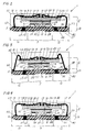
- Figure 1 shows a schematic cross section of an electronic component 1 of a first embodiment of the invention.
- the basis of this electronic component 1 is a rewiring substrate 5 with an upper side 36 and with an underside 40, which at the same time forms the underside of the electronic component 1.
- external contacts 30 are arranged in the form of contact balls, which are on external contact surfaces 27 of the rewiring substrate 5 are soldered.
- These external contact areas 27 of the rewiring substrate 5 are connected via through contacts 26 and via rewiring lines 25 of the rewiring substrate 5 to connection areas 6 and 60 on the upper side 36 of the rewiring substrate 5.
- the rewiring substrate 5 has a printed circuit board 23 as a carrier material.
- connection surfaces 6 for connecting to flip-chip contacts are arranged on the upper side 36 of the rewiring substrate 5.
- connection surfaces 60 for bond connections are arranged on the upper side 36 of the rewiring substrate 5.
- At least one logic chip 28 with its contact areas 24 is applied to the connection areas 6 of the center area 7 via the flipchip connections 8 as a first lower electronic module 9.
- the second electronic module 12 is a memory chip 39 which has a central bond channel 19 on its active upper side 32 with central bond connections 111. These central bond connections 111 of the bond channel 19 are connected via bond fingers 20 of the rewiring structure 13 to external contact areas 14 of the upper electronic component 12.
- the rewiring structure 13 has an intermediate substrate 41, on the edge regions of which the external contact areas 14 are arranged.
- the external contact areas 14 are via bond heads 33 of bond wires 18 with the connection areas 60 in the edge area 10 of the rewiring substrate 5 to form a bond sheet 34.
- a component housing 29 surrounds this stack 4 of at least one lower logic chip 28 and an upper memory chip 39 as well as the bond connections 18 between the upper memory chip 39 and the rewiring substrate 5.
- An underfill 37 which is a highly filled plastic with a degree of filling between 80 and 95% by weight. fills a gap between the active top side 35 of the logic chip 28 and the top side 36 of the rewiring substrate 5 and embeds the contact regions 24 of the logic chip 28. The high degree of filling ensures that the thermal expansion behavior of the underfill 37 is largely adapted to the thermal expansion behavior of the semiconductor material of the logic chip 28.
- a protective covering 22 covers the bonding channel 19 and protects the central bonding connections 111 of the memory chip 39. Between the protective covering 22 and the surrounding plastic housing compound 17 of the component housing 29 forms a material boundary 38.
- This electronic component 1 thus has a stack 4 made of a semiconductor chip 2 using flip-chip technology and an almost completely packaged electronic component 12.
- the functionality of this electronic component 12 has been tested under extreme temperatures between -50 and 150 ° C. before it is installed in the electronic component 1.
- This functionality test can be carried out either by connecting the external contact surfaces 14 of the upper electronic component 12 to a corresponding test socket or by temporarily applying external contacts to the external contact surfaces 14 after the test and before the installation in the electronic component 1 can be removed again.
- the underfill 37 is omitted, the gap between the active top 35 and the top 36 being filled with the plastic housing compound 17.
- FIG. 2 shows a schematic cross section of an electronic component 1 according to a second embodiment of the invention.
- Components with the same functions as in FIG. 1 are identified by the same reference symbols and are not discussed separately.
- a difference between the electronic component 1 from FIG. 1 and the electronic component 1 of the second embodiment of the invention consists in the fact that the bond wires 18 of the bond connections 11 with their bond heads 33 that stress the component height are arranged on the connection areas 60 in the edge regions 10 of the rewiring substrate 5.
- the relatively flat bond sheet 34 of such a bond connection 11 is arranged on the external contacts 14 of the upper electronic component 12. This makes it possible to limit the component height of the electronic component 1 through the protective sheath 22 of the bonding channel 19.
- the electronic component 1 thus has a lower height than the electronic component 1 from FIG. 1.
- the material boundary 38 between the plastic housing compound 17 and the plastic of the protective covering 22 of the bonding channel 19 is thus limited to the edge sides of the protective covering 22.
- FIG. 3 shows a schematic cross section of an electronic component 1 according to a third embodiment of the Invention.
- Components with the same functions as in the previous figures are identified by the same reference symbols and are not discussed separately.
- the structure of the stack of electronic components 9 and 12 is the same in the third embodiment of the invention as in the first embodiment of the invention from FIG. 1.
- the bonding channel 19 of the upper electronic component 12 is covered by the plastic housing compound 17, so that there is no material boundary 38 trained according to Figure 1.
- the method step for embedding the central bond connections 111 of the bond channel 19 in a protective sheath 22 is saved.
- the upper electronics module 12 can be tested for functionality before being installed in such an electronic component 1. It has the external contact surfaces 14 necessary for the function test.
- FIG. 4 shows a schematic cross section of an electronic component 1 of a fourth embodiment of the invention.
- Components with the same functions as in the previous figures are identified by the same reference symbols and are not discussed separately.
- This electronic component 1 of the fourth embodiment of the invention corresponds to the structure of the electronic component 1 from FIG. 2.
- the protective covering 22 of the bonding channel 19 for the upper electronic component 12 is omitted for reasons of cost savings. In this way, an electronic component 1 with a minimal component height can be implemented inexpensively.
- FIGS. 5 to 12 show schematic cross sections of intermediate products in the production of an electronic component 1 according to the first embodiment of the invention. Components with the same functions as in the previous figures are identified in FIGS. 5 to 12 with the same reference symbols and are not discussed separately.
- FIG. 5 shows a schematic cross section of a rewiring substrate 5.
- This rewiring substrate 5 is made from a printed circuit board 23 which is metallized on both sides and structured on both sides.
- the metal structure of the upper side 36 of the printed circuit board 23 is connected to the metal structure on the lower side 40 of the printed circuit board 23 via vias 26.
- the underside 40 of the printed circuit board 23 has external contact surfaces 27 which are arranged in 3 rings on the underside 40 of the printed circuit board 23.
- rewiring lines 21 are arranged, which are electrically connected to the through contacts 26.
- the rewiring lines 21 connect the through contacts 26 and thus the external contact areas 27 to connection areas 6 for the flipchip connections 8 in a central area 7 of the printed circuit board 23 and / or to connection areas 60 for the bond connections 18 in edge areas 10 of the printed circuit board 23.
- FIG. 6 shows a schematic cross section of a rewiring substrate 5 with an applied first electronic module 9.
- This electronic module 9 is connected to the connection areas 6 of the central region 7 of the rewiring substrate 5 via flip chip connections 8.
- the space between the active upper side 35 of the first lower electronic component 9 and the upper side 36 of the rewiring substrate 5 is filled with an underfill 37.
- FIG. 7 shows a schematic cross section of an electronic component 12 with an unprotected bond channel 19.
- this second electronic component 12 has a rewiring structure 13 with an intermediate substrate 41.
- this second electronic component 12 has a bond channel 19 with central bond connections 111, which are connected to external contact areas 14 of the electronic component 12 via the rewiring structure 13.
- An electronic module 12 prepared in this way is exposed to extreme temperatures between -50 and 150 ° C. before being installed in an electronic component, while its functionality is checked. This function test is also carried out without the central bond connections 111 in the bond channel 19 already being protected by a protective sheath.
- FIG. 8 shows a schematic cross section of the second electronics module 12 from FIG. 7 with a protected bonding channel 19.
- the handling of the second electronics module 12 is easier due to the protected bonding channel 19 compared to the handling of an electronics module 12 with an unprotected bonding channel 19, as shown in FIG. 7 and safer.
- the sensitive central bond connections 111 are namely embedded in the protective covering 22 and protected against mechanical damage during handling.
- FIG. 9 shows a schematic cross section through a stack 4 of a first and second electronics module 9 or 12 on the rewiring substrate 5 from FIG. 5.
- FIG. 10 shows a schematic cross section through a stack 4 from FIG. 9 after the application of bond connections 11.
- These bond connections 11 are applied to the external contact areas 14 of the rewiring structure 13 of the upper electronic module 12.
- a bond head 33 is first bonded to the external contact areas 14 and the bond wire 18 is guided downward to the connection areas 60 of the rewiring substrate 5.
- the bond wires 18 are then connected to the connection pads 60 to form a bond bow 34.
- FIG. 11 shows a schematic cross section through an electronic component 1 after the stack 4 from FIG. 10 has been packaged in a component housing 29.
- the rewiring substrate 5 with its underside 40 simultaneously forms the underside of the electronic component 1.
- a material boundary 38 is formed between the Material of the protective sheath 22 of the bond channel 19 and the plastic housing compound 17.
- FIG. 12 shows a schematic cross section through an electronic component 1 after application of external contacts 30 to the rewiring substrate 5.
- These external contacts 30 are designed here as contact balls and arranged in 3 rings.
- solderable contact balls are soldered onto the outer contact surfaces 27 on the underside 40 of the rewiring structure 5.
Landscapes
- Engineering & Computer Science (AREA)
- Power Engineering (AREA)
- Microelectronics & Electronic Packaging (AREA)
- Physics & Mathematics (AREA)
- Condensed Matter Physics & Semiconductors (AREA)
- General Physics & Mathematics (AREA)
- Computer Hardware Design (AREA)
- Wire Bonding (AREA)
Applications Claiming Priority (2)
| Application Number | Priority Date | Filing Date | Title |
|---|---|---|---|
| DE10244664 | 2002-09-24 | ||
| DE10244664A DE10244664A1 (de) | 2002-09-24 | 2002-09-24 | Elektronisches Bauteil mit Halbleiterchips in einem Stapel und Verfahren zur Herstellung desselben |
Publications (2)
| Publication Number | Publication Date |
|---|---|
| EP1403921A2 true EP1403921A2 (fr) | 2004-03-31 |
| EP1403921A3 EP1403921A3 (fr) | 2006-02-15 |
Family
ID=31969560
Family Applications (1)
| Application Number | Title | Priority Date | Filing Date |
|---|---|---|---|
| EP03017506A Withdrawn EP1403921A3 (fr) | 2002-09-24 | 2003-08-04 | Dispositif electronique avec des puces semi-conductrices empilées et procédé de fabrication associée |
Country Status (3)
| Country | Link |
|---|---|
| US (1) | US7190059B2 (fr) |
| EP (1) | EP1403921A3 (fr) |
| DE (1) | DE10244664A1 (fr) |
Families Citing this family (8)
| Publication number | Priority date | Publication date | Assignee | Title |
|---|---|---|---|---|
| CN100401515C (zh) * | 2004-11-19 | 2008-07-09 | 矽品精密工业股份有限公司 | 包覆有倒装芯片封装件的半导体装置及其制法 |
| KR100651125B1 (ko) * | 2005-03-21 | 2006-12-01 | 삼성전자주식회사 | 이중 성형된 멀티 칩 패키지 및 그 제조 방법 |
| DE102005025754B4 (de) * | 2005-06-02 | 2019-08-08 | Infineon Technologies Ag | Halbleitersensorbauteil mit einem Sensorchip und Verfahren zur Herstellung von Halbleitersensorbauteilen |
| US8022539B2 (en) * | 2008-11-17 | 2011-09-20 | Stats Chippac Ltd. | Integrated circuit packaging system with increased connectivity and method of manufacture thereof |
| KR101047139B1 (ko) * | 2009-11-11 | 2011-07-07 | 삼성전기주식회사 | 단층 보드온칩 패키지 기판 및 그 제조방법 |
| US8850196B2 (en) * | 2010-03-29 | 2014-09-30 | Motorola Solutions, Inc. | Methods for authentication using near-field |
| US8871549B2 (en) | 2013-02-14 | 2014-10-28 | International Business Machines Corporation | Biological and chemical sensors |
| US9312198B2 (en) * | 2013-03-15 | 2016-04-12 | Intel Deutschland Gmbh | Chip package-in-package and method thereof |
Citations (4)
| Publication number | Priority date | Publication date | Assignee | Title |
|---|---|---|---|---|
| US5384689A (en) * | 1993-12-20 | 1995-01-24 | Shen; Ming-Tung | Integrated circuit chip including superimposed upper and lower printed circuit boards |
| EP1045443A2 (fr) * | 1999-04-14 | 2000-10-18 | Sharp Kabushiki Kaisha | Dispositif à semi-conducteur et methode de fabrication associée |
| US6420789B1 (en) * | 2000-05-16 | 2002-07-16 | Micron Technology, Inc. | Ball grid array chip packages having improved testing and stacking characteristics |
| EP1317001A1 (fr) * | 2001-11-30 | 2003-06-04 | Infineon Technologies AG | Dispositif à semi-conducteur |
Family Cites Families (17)
| Publication number | Priority date | Publication date | Assignee | Title |
|---|---|---|---|---|
| US31864A (en) * | 1861-04-02 | Improvement in sewing-machines | ||
| US31867A (en) * | 1861-04-02 | Brake eor carriages | ||
| US6784023B2 (en) | 1996-05-20 | 2004-08-31 | Micron Technology, Inc. | Method of fabrication of stacked semiconductor devices |
| US6885092B1 (en) * | 1997-09-29 | 2005-04-26 | Hitachi, Ltd. | Semiconductor device and a memory system including a plurality of IC chips in a common package |
| US6392304B1 (en) * | 1998-11-12 | 2002-05-21 | United Memories, Inc. | Multi-chip memory apparatus and associated method |
| KR100533673B1 (ko) * | 1999-09-03 | 2005-12-05 | 세이코 엡슨 가부시키가이샤 | 반도체 장치 및 그 제조 방법, 회로 기판 및 전자 기기 |
| JP2001094045A (ja) * | 1999-09-22 | 2001-04-06 | Seiko Epson Corp | 半導体装置 |
| KR100379600B1 (ko) * | 2000-08-14 | 2003-04-10 | 삼성전자주식회사 | 듀얼 칩 패키지의 제조 방법 |
| DE10043450A1 (de) * | 2000-09-04 | 2002-03-14 | Orient Semiconductor Elect Ltd | Verbessertes Verfahren zum Montieren von Chips in Flip-Chip-Technik-Prozessen |
| JP2002093831A (ja) | 2000-09-14 | 2002-03-29 | Shinko Electric Ind Co Ltd | 半導体装置およびその製造方法 |
| JP4571320B2 (ja) * | 2001-02-02 | 2010-10-27 | Okiセミコンダクタ株式会社 | 半導体チップパッケージ |
| JP2002280516A (ja) * | 2001-03-19 | 2002-09-27 | Toshiba Corp | 半導体モジュール |
| US6441483B1 (en) * | 2001-03-30 | 2002-08-27 | Micron Technology, Inc. | Die stacking scheme |
| JP2003197856A (ja) * | 2001-12-28 | 2003-07-11 | Oki Electric Ind Co Ltd | 半導体装置 |
| TW529141B (en) * | 2002-01-07 | 2003-04-21 | Advanced Semiconductor Eng | Stacking type multi-chip package and its manufacturing process |
| SG121705A1 (en) * | 2002-02-21 | 2006-05-26 | United Test & Assembly Ct Ltd | Semiconductor package |
| US6472736B1 (en) * | 2002-03-13 | 2002-10-29 | Kingpak Technology Inc. | Stacked structure for memory chips |
-
2002
- 2002-09-24 DE DE10244664A patent/DE10244664A1/de not_active Withdrawn
-
2003
- 2003-08-04 EP EP03017506A patent/EP1403921A3/fr not_active Withdrawn
- 2003-09-24 US US10/669,539 patent/US7190059B2/en not_active Expired - Fee Related
Patent Citations (4)
| Publication number | Priority date | Publication date | Assignee | Title |
|---|---|---|---|---|
| US5384689A (en) * | 1993-12-20 | 1995-01-24 | Shen; Ming-Tung | Integrated circuit chip including superimposed upper and lower printed circuit boards |
| EP1045443A2 (fr) * | 1999-04-14 | 2000-10-18 | Sharp Kabushiki Kaisha | Dispositif à semi-conducteur et methode de fabrication associée |
| US6420789B1 (en) * | 2000-05-16 | 2002-07-16 | Micron Technology, Inc. | Ball grid array chip packages having improved testing and stacking characteristics |
| EP1317001A1 (fr) * | 2001-11-30 | 2003-06-04 | Infineon Technologies AG | Dispositif à semi-conducteur |
Also Published As
| Publication number | Publication date |
|---|---|
| US20040063304A1 (en) | 2004-04-01 |
| US7190059B2 (en) | 2007-03-13 |
| DE10244664A8 (de) | 2004-07-15 |
| EP1403921A3 (fr) | 2006-02-15 |
| DE10244664A1 (de) | 2004-04-01 |
Similar Documents
| Publication | Publication Date | Title |
|---|---|---|
| DE10259221B4 (de) | Elektronisches Bauteil mit einem Stapel aus Halbleiterchips und Verfahren zur Herstellung desselben | |
| DE10333841B4 (de) | Verfahren zur Herstellung eines Nutzens mit in Zeilen und Spalten angeordneten Halbleiterbauteilpositionen und Verfahren zur Herstellung eines Halbleiterbauteils | |
| DE10045043B4 (de) | Halbleiterbauteil und Verfahren zu dessen Herstellung | |
| DE10234951B4 (de) | Verfahren zur Herstellung von Halbleiterschaltungsmodulen | |
| DE102011053871A1 (de) | Multichip-Halbleitergehäuse und deren Zusammenbau | |
| DE10142119B4 (de) | Elektronisches Bauteil und Verfahren zu seiner Herstellung | |
| WO2004015770A1 (fr) | Support de circuit a plusieurs couches et fabrication dudit support | |
| DE10251530A1 (de) | Stapelanordnung eines Speichermoduls | |
| EP1490908B1 (fr) | Module de puissance comportant au moins deux substrats et procede permettant de le produire | |
| EP1614158A2 (fr) | Module multipuces comportant plusieurs puces de semiconducteur et carte de circuits comportant plusieurs composants | |
| WO1999045592A1 (fr) | Composant semi-conducteur comprenant plusieurs puces semi-conductrices | |
| DE102010029522B4 (de) | Verspannungsverringerung beim Einbringen eines Chips in ein Gehäuse mittels eines um den Chip herum ausgebildeten Spannungskompensationsgebiets | |
| DE10124970B4 (de) | Elektronisches Bauteil mit einem Halbleiterchip auf einer Halbleiterchip-Anschlußplatte, Systemträger und Verfahren zu deren Herstellung | |
| EP1403921A2 (fr) | Dispositif electronique avec des puces semi-conductrices empilées et procédé de fabrication associée | |
| DE102004036909B4 (de) | Halbleiterbasisbauteil mit Verdrahtungssubstrat und Zwischenverdrahtungsplatte für einen Halbleiterbauteilstapel sowie Verfahren zu deren Herstellung | |
| DE10136655C1 (de) | Multichipmodul in COB Bauweise, insbesondere CompactFlash Card mit hoher Speicherkapazität und Verfahren zur Herstellung desselben | |
| DE10162676B4 (de) | Elektronisches Bauteil mit einem Halbleiterchip und einer Umverdrahtungsplatte und Systemträger für mehrere elektronische Bauteile sowie Verfahren zur Herstellung derselben | |
| DE102004050178B3 (de) | Flip-Chip-Bauelement | |
| DE19821916C2 (de) | Halbleitereinrichtung mit einem BGA-Substrat | |
| DE19702186C2 (de) | Verfahren zur Gehäusung von integrierten Schaltkreisen | |
| DE102007050433B4 (de) | Halbleitermodul, Verfahren zum Herstellen eines Halbleitermoduls und Board mit einem Halbleitermodul | |
| DE102006024147B3 (de) | Elektronisches Modul mit Halbleiterbauteilgehäuse und einem Halbleiterchip und Verfahren zur Herstellung desselben | |
| DE102007002807B4 (de) | Chipanordnung | |
| DE10133571B4 (de) | Elektronisches Bauteil und Verfahren zu seiner Herstellung | |
| DE10261410B4 (de) | Verfahren zur Verbindung einer integrierten Schaltung mit einem Substrat und entsprechende Schaltungsanordnung |
Legal Events
| Date | Code | Title | Description |
|---|---|---|---|
| PUAI | Public reference made under article 153(3) epc to a published international application that has entered the european phase |
Free format text: ORIGINAL CODE: 0009012 |
|
| AK | Designated contracting states |
Kind code of ref document: A2 Designated state(s): AT BE BG CH CY CZ DE DK EE ES FI FR GB GR HU IE IT LI LU MC NL PT RO SE SI SK TR |
|
| AX | Request for extension of the european patent |
Extension state: AL LT LV MK |
|
| PUAL | Search report despatched |
Free format text: ORIGINAL CODE: 0009013 |
|
| AK | Designated contracting states |
Kind code of ref document: A3 Designated state(s): AT BE BG CH CY CZ DE DK EE ES FI FR GB GR HU IE IT LI LU MC NL PT RO SE SI SK TR |
|
| AX | Request for extension of the european patent |
Extension state: AL LT LV MK |
|
| RIC1 | Information provided on ipc code assigned before grant |
Ipc: H01L 25/065 20060101ALI20051228BHEP Ipc: H01L 21/98 20060101AFI20031126BHEP |
|
| 17P | Request for examination filed |
Effective date: 20060203 |
|
| AKX | Designation fees paid |
Designated state(s): DE FR IT |
|
| 17Q | First examination report despatched |
Effective date: 20090910 |
|
| RAP1 | Party data changed (applicant data changed or rights of an application transferred) |
Owner name: INFINEON TECHNOLOGIES AG |
|
| STAA | Information on the status of an ep patent application or granted ep patent |
Free format text: STATUS: THE APPLICATION IS DEEMED TO BE WITHDRAWN |
|
| 18D | Application deemed to be withdrawn |
Effective date: 20100121 |