EP1403869A2 - Dispositif et méthode pour constituer un signal - Google Patents
Dispositif et méthode pour constituer un signal Download PDFInfo
- Publication number
- EP1403869A2 EP1403869A2 EP20030025667 EP03025667A EP1403869A2 EP 1403869 A2 EP1403869 A2 EP 1403869A2 EP 20030025667 EP20030025667 EP 20030025667 EP 03025667 A EP03025667 A EP 03025667A EP 1403869 A2 EP1403869 A2 EP 1403869A2
- Authority
- EP
- European Patent Office
- Prior art keywords
- run length
- sync
- sync signal
- signal
- sector
- Prior art date
- Legal status (The legal status is an assumption and is not a legal conclusion. Google has not performed a legal analysis and makes no representation as to the accuracy of the status listed.)
- Granted
Links
Images


Classifications
-
- H—ELECTRICITY
- H03—ELECTRONIC CIRCUITRY
- H03M—CODING; DECODING; CODE CONVERSION IN GENERAL
- H03M5/00—Conversion of the form of the representation of individual digits
- H03M5/02—Conversion to or from representation by pulses
- H03M5/04—Conversion to or from representation by pulses the pulses having two levels
- H03M5/14—Code representation, e.g. transition, for a given bit cell depending on the information in one or more adjacent bit cells, e.g. delay modulation code, double density code
- H03M5/145—Conversion to or from block codes or representations thereof
-
- H—ELECTRICITY
- H04—ELECTRIC COMMUNICATION TECHNIQUE
- H04L—TRANSMISSION OF DIGITAL INFORMATION, e.g. TELEGRAPHIC COMMUNICATION
- H04L7/00—Arrangements for synchronising receiver with transmitter
-
- G—PHYSICS
- G11—INFORMATION STORAGE
- G11B—INFORMATION STORAGE BASED ON RELATIVE MOVEMENT BETWEEN RECORD CARRIER AND TRANSDUCER
- G11B20/00—Signal processing not specific to the method of recording or reproducing; Circuits therefor
- G11B20/10—Digital recording or reproducing
- G11B20/14—Digital recording or reproducing using self-clocking codes
- G11B20/1403—Digital recording or reproducing using self-clocking codes characterised by the use of two levels
- G11B20/1423—Code representation depending on subsequent bits, e.g. delay modulation, double density code, Miller code
- G11B20/1426—Code representation depending on subsequent bits, e.g. delay modulation, double density code, Miller code conversion to or from block codes or representations thereof
-
- H—ELECTRICITY
- H04—ELECTRIC COMMUNICATION TECHNIQUE
- H04L—TRANSMISSION OF DIGITAL INFORMATION, e.g. TELEGRAPHIC COMMUNICATION
- H04L25/00—Baseband systems
- H04L25/38—Synchronous or start-stop systems, e.g. for Baudot code
- H04L25/40—Transmitting circuits; Receiving circuits
- H04L25/49—Transmitting circuits; Receiving circuits using code conversion at the transmitter; using predistortion; using insertion of idle bits for obtaining a desired frequency spectrum; using three or more amplitude levels ; Baseband coding techniques specific to data transmission systems
- H04L25/4906—Transmitting circuits; Receiving circuits using code conversion at the transmitter; using predistortion; using insertion of idle bits for obtaining a desired frequency spectrum; using three or more amplitude levels ; Baseband coding techniques specific to data transmission systems using binary codes
-
- H—ELECTRICITY
- H04—ELECTRIC COMMUNICATION TECHNIQUE
- H04L—TRANSMISSION OF DIGITAL INFORMATION, e.g. TELEGRAPHIC COMMUNICATION
- H04L7/00—Arrangements for synchronising receiver with transmitter
- H04L7/04—Speed or phase control by synchronisation signals
- H04L7/041—Speed or phase control by synchronisation signals using special codes as synchronising signal
Definitions
- the invention relates to a method of transmitting digital data in which digital data is retained in sectors each comprising a plurality of sync frames and sequentially transmitting it (including recording of the digital data).
- EFM EFM modulation signal
- connection bits of three bits are added to intervals among the respective converted data, and the resultant data is formed as an EFM modulation signal.
- a bit train of the connection bits is set so as to satisfy the foregoing run length limitation.
- a signal obtained by adding a sync signal to the EFM modulation signal has been recorded.
- the sequence by the EFM modulation signals is constructed in a manner such that a repetitive pattern of maximum interval which corresponds to the maximum run length k, namely, repetitive pattern such as 11T - 11T doesn't exist in the sequence and the repetitive pattern of 11T is used as a sync signal.
- the sync signal is extracted by detecting the repetitive pattern of 11T from a signal read out from the CD.
- the invention is made to solve the problems mentioned above and it is an object of the invention to provide a transmitting method of digital data whereby the digital data can be reproduced at a high precision even at the time of a high-density recording or a high-density data transmission.
- a transmitting method of digital data for retaining digital data in sectors each comprising a plurality of sync frames and sequentially transmitting, wherein the sync frame comprises a sync signal and a run length limited code which corresponds to the digital data and satisfies limitations of a minimum run length and a maximum run length, and the sync signal includes a sync pattern comprising a bit pattern having a run length which is longer than the maximum run length by 3T and addition bit patterns which are arranged before and after the bit pattern and each of which has a run length that is longer than the minimum run length.
- a transmitting method of digital data for storing the digital data into sectors each comprising a plurality of sync frames and sequentially transmitting, wherein the sync frame comprises a sync signal and a run length limited code which corresponds to the digital data and satisfies limitations regarding a minimum run length and a maximum run length, and the sync signal includes a specific code which indicates a position in the sector and which enables a DC control to be performed.
- the sync frame is comprised of the sync signal and the run length limited code which satisfies the limitations of the minimum run length and the maximum run length
- the sync signal includes the sync pattern comprising the bit pattern of the run length that is longer than the maximum run length by 3T and the addition bit patterns which are arranged before and after the bit pattern and each of which has a run length that is longer than the minimum run length.
- the sync signal includes the specific code which indicates the position in the sector and which enables the DC control to be performed.
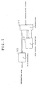
- Fig. 1 is a diagram showing a construction of a transmission signal forming apparatus for forming a transmission signal by a transmitting method of digital data according to the invention.
- All of code words obtained by the 8-16 modulator 10 have pattern forms which satisfy any one of the following conditions of Next_State1 to Next_State4.
- the modulating method has been published by the following paper.
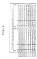
- a sync signal generating circuit 20 generates 32 sync signals having different bit patterns as shown in Figs. 2 and 3 and transmits them to a synthesizing circuit 30 which preferably includes a CPU and a memory as described later.
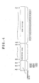
- Fig. 4 is a diagram showing a format of the sync signal.
- bits 1 to 3 of the sync signal denote connection bits provided so as to satisfy the foregoing limitations of the minimum run length d and the maximum run length k when the sync signal is connected to a code word just before it.
- a connection bit pattern by bits 1 to 3 indicate any one of ⁇ 000 ⁇ , ⁇ 001 ⁇ , and ⁇ 100 ⁇ .
- a sync pattern to identify the sync signal is allocated to bits 11 to 32 of the sync signal.
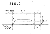
- the sync pattern is a bit pattern of an arrangement such as (4T or more - 14T - 4T) in which a pattern of 14T that is larger than the maximum interval 11T in the 8-16 modulation signal by 3T is set to a nucleus and a pattern of a fixed length of 4T and a pattern of 4T or more are arranged after and before the pattern of 14T, respectively, namely, bit pattern of
- the sync pattern is a fixed pattern which is common to all sync signals as shown in Figs. 2 and 3.
- the sync pattern even when the 11T pattern in the 8-16 modulation signal is edge-shifted due to an influence by an inter-symbol interference and is changed to a pattern of 12T and, further, the sync pattern itself is edge-shifted and is shortened by only 1T, in order enable both of them to be distinguished, the pattern of 14T that is larger than the maximum interval 11T in the 8-16 modulation signal by 3T is used.
- the 14T pattern denotes a shortest length which can be set when considering the edge-shift.
- an addition bit pattern of a fixed length of 4T and an addition bit pattern of 4T or more after and before the 14T pattern an interval that is larger than the shortest bits of 3T by at least 1T is provided, thereby reducing an influence by the inter-symbol interference with a neighboring mark.
- Fig. 5 is a diagram showing a transmission signal waveform by the sync pattern.
- the edge interval can be stably detected.
- the selected pattern can be used as a signal for a speed detection of a spindle servo upon starting.
- mark lengths before and after the 14T pattern By setting mark lengths before and after the 14T pattern to be equal to or larger than 4T in which an amplitude is larger than the shortest mark length, a permissible amplitude is increased for a fluctuation of the slice level.
- a rear mark length is set to 4T and a front mark length is set to 4T or more.
- the reason why the rear pattern of the 14T pattern is set to the fixed length of 4T and the front pattern is set to 4T or more is because when a specific code, which will be described hereinafter, is further set before the 14T pattern, a degree of freedom of the front pattern is increased and the number of patterns to be obtained as a specific code is sufficiently assured.
- the specific code is allocated to bits 4 to 10 of the sync signal.
- a position in one sector which will be explained hereinafter, can be identified.
- the synthesizing circuit 30 in Fig. 1 selects any one of the sync signals generated by the sync signal generating circuit 20 every train of the 8-16 modulation signals which are sequentially supplied from the 8-16 modulator 10, namely, every 91 code words and generates a signal obtained by adding the selected sync signal to the head of the 91 code words as a transmission signal corresponding to one sync frame.
- Fig. 6 is a diagram showing a format of the transmission signal per one sector which is generated by the synthesizing circuit 30.
- one sector comprises 13 lines. Two sync frames are allocated to each line.
- the sync signal allocated to each sync frame is selected from the 32 kinds of sync signals shown in Figs. 2 and 3.
- the sync signal allocated to a front sync frame of the first line corresponds to SY0 selected from the 32 kinds of sync signals.
- the sync signal which is allocated to the front sync frame is cyclically repeated like SY1 to SY4 in accordance with an increase in number of line. Differences among SY1 to SY4 are decided by the specific code and connection bits.
- a CPU central processing unit
- a memory they are not shown
- the CPU in the synthesizing circuit 30 first sets 1 as an initial address into a built-in register n (step S1).
- the CPU reads out information corresponding to the address stored in the register n from the memory shown in Fig. 8, respectively and stores the information into registers X and Y (step S2).
- SY0 and SY5 stored in address 1 in the memory in Fig. 8 are read out and stored into the registers X and Y, respectively.
- the CPU selects the sync signal corresponding to the storage contents in the register X from the 32 kinds of sync signals shown in Figs. 2 and 3 which are supplied from the sync signal generating circuit 20.
- SY0 has been stored in the register X
- the signal corresponding to SY0 is selected from the 32 kinds of sync signals shown in Figs. 2 and 3.
- the code word existing just before the sync signal is Next_State1 (the number of continuous 0 at the termination is equal to 1 or 0) or Next_State2 (the number of continuous 0 at the termination is equal to 2 to 5)
- the CPU selects the sync signal in which the connection bit pattern by bits 1 to 3 is set to ⁇ 000 ⁇ from SY0 shown in Figs. 2 and 3.
- the CPU selects the pattern which is optimum for the DC suppression from the two kinds of patterns and sets the selected pattern to final SY0.
- the CPU selects the sync signal corresponding to the storage contents in the register Y. For example, when SY5 has been stored in the register Y, the sync signal corresponding to SY5 is selected from the 32 kinds of sync signals shown in Figs. 2 and 3.
- the code word existing just before the sync signal is Next_State3 (the number of continuous 0 at the termination is equal to 2 to 5) or Next_State4 (the number of continuous 0 at the termination is equal to 6 to 9)
- the CPU selects the sync signal in which the connection bit pattern by bits 1 to 3 is equal to ⁇ 100 ⁇ from SY5 shown in Figs. 2 and 3.
- the CPU selects the pattern which is optimum for the DC suppression from the two kinds of patterns and sets the selected pattern to final SY5 (step S3).
- the CPU generates a pattern obtained by serially connecting the 8-16 modulation signal of 91 code words to each of the sync signals selected on the basis of the storage contents of the registers X and Y as mentioned above as a transmission signal of one line as shown in Fig. 6 (step S4).
- step S5 The CPU judges whether the contents in the register n are larger than 13 or not (step S5). In step S5, until it is decided that the contents in the register n are larger than 13, the CPU adds 1 to the contents in the register n (step S6) and, after that, repetitively executes the operations in step S2 and subsequent steps.
- the transmission signals of the first to 13th lines (of one sector) as shown in Fig. 6 are sequentially generated by the repetitive operation.
- a decoder side which receives the transmission signal with the structure executes an error correcting process by using the transmission signals each of which has the sector structure as shown in Fig. 6 and which are collected by the number as many as 16 sectors as one error-correction block.
- the decoder it is important that after completion of the reception of the transmission signal, the head of the sector is searched, an address recorded is subsequently immediately read out, and data of the error-correction block is collected.
- the 32 kinds of sync signals having different bit patterns are prepared and, further, as shown in Fig. 6, the combination pattern of the sync signal to be allocated to each line in one sector is set to a unique pattern every line.
- the sync signal in the front sync frame existing at the head of each line is cyclically repeated like SY1 to SY4 in accordance with an increase in number of lines.
- the line in one sector can be specified by recognizing the combination pattern of the sync signals, so that the position of SY0 at the sector head can be predicted.
- a preventing function can be further raised for a read error of the sync signal by recognizing the repetitive patterns of SY1 to SY4. Since the line is specified on the basis of the combination pattern of the two sync signals existing in one line, it is sufficient to use eight kinds of SY0 to SY7 as kinds of sync signals in one sector.
- SY0 is selected in a manner such that an inter-code distance between SY0 and the head syncs (SY1 to SY4) of each of the other lines becomes maximum.
- the inter-code distance denotes a similarity between the sync signals.
- the sync signal is a signal of the largest distance.
- the number of shifting times of the position of 1 until the signal coincides with a sync signal is set to the distance with the sync signal.
- the sync signal which is relatively similar to SY0 is set to the intermediate sync signal (SY5 to SY7) of each line, and a common sync signal is not used in the head and middle portions of each line.
- the common sync signal is not used in the head and middle portions of the line, there is also an effect such that a probability such that the head and middle portions of each line is erroneously recognized by the read error is reduced.
- the sync frame comprises the sync signal and the run length limited code which satisfies the limitations of the minimum run length and the maximum run length
- the sync signal includes the sync pattern comprised of the bit pattern of a run length which is longer than the maximum run length by 3T and the addition bit patterns which are arranged before and after the bit pattern and each of which has a run length that is longer than the minimum run length.
- the sync signal includes the specific code which indicates the position in the sector and which enables the DC control to be performed.
Landscapes
- Engineering & Computer Science (AREA)
- Signal Processing (AREA)
- Computer Networks & Wireless Communication (AREA)
- Theoretical Computer Science (AREA)
- Physics & Mathematics (AREA)
- Spectroscopy & Molecular Physics (AREA)
- Signal Processing For Digital Recording And Reproducing (AREA)
- Synchronisation In Digital Transmission Systems (AREA)
- Dc Digital Transmission (AREA)
- Compression, Expansion, Code Conversion, And Decoders (AREA)
Priority Applications (4)
| Application Number | Priority Date | Filing Date | Title |
|---|---|---|---|
| EP06115012A EP1715484A3 (fr) | 1995-12-05 | 1996-12-05 | Appareil et procédé de formation de signaux |
| EP06115021A EP1715486B1 (fr) | 1995-12-05 | 1996-12-05 | Appareil et procédé de formation de signaux |
| EP06115028A EP1715487A3 (fr) | 1995-12-05 | 1996-12-05 | Appareil et procédé de formation de signaux |
| EP06115016A EP1715485B1 (fr) | 1995-12-05 | 1996-12-05 | Appareil et procédé de formation de signaux |
Applications Claiming Priority (3)
| Application Number | Priority Date | Filing Date | Title |
|---|---|---|---|
| JP31642095A JP3394127B2 (ja) | 1995-12-05 | 1995-12-05 | ディジタルデータの伝送方法 |
| JP31642095 | 1995-12-05 | ||
| EP96119545A EP0779623B1 (fr) | 1995-12-05 | 1996-12-05 | Méthode de transmission de données digitales |
Related Parent Applications (3)
| Application Number | Title | Priority Date | Filing Date |
|---|---|---|---|
| EP96119545.0 Division | 1996-12-05 | ||
| EP96119545A Division-Into EP0779623B1 (fr) | 1995-12-05 | 1996-12-05 | Méthode de transmission de données digitales |
| EP96119545A Division EP0779623B1 (fr) | 1995-12-05 | 1996-12-05 | Méthode de transmission de données digitales |
Related Child Applications (4)
| Application Number | Title | Priority Date | Filing Date |
|---|---|---|---|
| EP06115021A Division EP1715486B1 (fr) | 1995-12-05 | 1996-12-05 | Appareil et procédé de formation de signaux |
| EP06115016A Division EP1715485B1 (fr) | 1995-12-05 | 1996-12-05 | Appareil et procédé de formation de signaux |
| EP06115012A Division EP1715484A3 (fr) | 1995-12-05 | 1996-12-05 | Appareil et procédé de formation de signaux |
| EP06115028A Division EP1715487A3 (fr) | 1995-12-05 | 1996-12-05 | Appareil et procédé de formation de signaux |
Publications (3)
| Publication Number | Publication Date |
|---|---|
| EP1403869A2 true EP1403869A2 (fr) | 2004-03-31 |
| EP1403869A3 EP1403869A3 (fr) | 2004-05-12 |
| EP1403869B1 EP1403869B1 (fr) | 2007-02-14 |
Family
ID=18076885
Family Applications (6)
| Application Number | Title | Priority Date | Filing Date |
|---|---|---|---|
| EP06115021A Expired - Lifetime EP1715486B1 (fr) | 1995-12-05 | 1996-12-05 | Appareil et procédé de formation de signaux |
| EP03025667A Expired - Lifetime EP1403869B1 (fr) | 1995-12-05 | 1996-12-05 | Dispositif et méthode pour constituer un signal |
| EP06115012A Withdrawn EP1715484A3 (fr) | 1995-12-05 | 1996-12-05 | Appareil et procédé de formation de signaux |
| EP06115016A Expired - Lifetime EP1715485B1 (fr) | 1995-12-05 | 1996-12-05 | Appareil et procédé de formation de signaux |
| EP06115028A Withdrawn EP1715487A3 (fr) | 1995-12-05 | 1996-12-05 | Appareil et procédé de formation de signaux |
| EP96119545A Expired - Lifetime EP0779623B1 (fr) | 1995-12-05 | 1996-12-05 | Méthode de transmission de données digitales |
Family Applications Before (1)
| Application Number | Title | Priority Date | Filing Date |
|---|---|---|---|
| EP06115021A Expired - Lifetime EP1715486B1 (fr) | 1995-12-05 | 1996-12-05 | Appareil et procédé de formation de signaux |
Family Applications After (4)
| Application Number | Title | Priority Date | Filing Date |
|---|---|---|---|
| EP06115012A Withdrawn EP1715484A3 (fr) | 1995-12-05 | 1996-12-05 | Appareil et procédé de formation de signaux |
| EP06115016A Expired - Lifetime EP1715485B1 (fr) | 1995-12-05 | 1996-12-05 | Appareil et procédé de formation de signaux |
| EP06115028A Withdrawn EP1715487A3 (fr) | 1995-12-05 | 1996-12-05 | Appareil et procédé de formation de signaux |
| EP96119545A Expired - Lifetime EP0779623B1 (fr) | 1995-12-05 | 1996-12-05 | Méthode de transmission de données digitales |
Country Status (11)
| Country | Link |
|---|---|
| US (2) | US5987066A (fr) |
| EP (6) | EP1715486B1 (fr) |
| JP (1) | JP3394127B2 (fr) |
| KR (1) | KR100329456B1 (fr) |
| CN (4) | CN1287546C (fr) |
| DE (4) | DE69638200D1 (fr) |
| HK (1) | HK1004500A1 (fr) |
| MX (1) | MX9606099A (fr) |
| MY (1) | MY112856A (fr) |
| SG (1) | SG79210A1 (fr) |
| TW (1) | TW311195B (fr) |
Families Citing this family (25)
| Publication number | Priority date | Publication date | Assignee | Title |
|---|---|---|---|---|
| JP3962439B2 (ja) * | 1996-06-21 | 2007-08-22 | パイオニア株式会社 | 情報記録装置及び情報記録方法並びに情報再生装置及び情報再生方法 |
| JP3729362B2 (ja) * | 1996-07-15 | 2005-12-21 | ソニー株式会社 | 記録媒体再生装置および記録媒体再生方法 |
| JP3814966B2 (ja) * | 1997-08-14 | 2006-08-30 | ソニー株式会社 | 記録媒体、データ伝送装置、データ受信装置及び光ディスク装置 |
| JP3870573B2 (ja) | 1998-08-24 | 2007-01-17 | ソニー株式会社 | 変調装置および方法、記録媒体、並びに復調装置および方法 |
| US6768706B1 (en) * | 1998-10-28 | 2004-07-27 | Victor Company Of Japan, Ltd | Frequency control apparatus and digital signal reproducing apparatus |
| EP1045391A1 (fr) * | 1999-04-16 | 2000-10-18 | Koninklijke Philips Electronics N.V. | Méthode et dispositif d'enregistrement d'information sous forme d'unités |
| DE60126428T2 (de) * | 2000-12-26 | 2007-11-08 | Matsushita Electric Industrial Co., Ltd., Kadoma | Aufzeichnung zusätzlicher daten mit verbindenden rahmen und verschiedenen synchronisationssignalen |
| JP4633763B2 (ja) * | 2000-12-26 | 2011-02-16 | パナソニック株式会社 | 記録媒体、記録方法、再生方法、記録装置および再生装置 |
| KR100669623B1 (ko) * | 2001-03-12 | 2007-01-15 | 엘지전자 주식회사 | 디지털 데이터 변환방법 |
| JP3964634B2 (ja) | 2001-06-14 | 2007-08-22 | 株式会社東芝 | 同期コード生成方法、情報記録方法、情報再生方法、情報再生装置及び情報記憶媒体 |
| JP2003085898A (ja) | 2001-09-12 | 2003-03-20 | Toshiba Corp | 情報記憶媒体、情報記録装置、情報記録方法、情報再生装置、及び情報再生装置 |
| KR20040071704A (ko) * | 2001-12-07 | 2004-08-12 | 코닌클리케 필립스 일렉트로닉스 엔.브이. | 엠.에이.엠.엠.오.에스 판독에서의 증가된 분해능과 파워마진을 위한 비대칭 런길이 제약 |
| JP4130884B2 (ja) | 2002-09-09 | 2008-08-06 | ソニー株式会社 | 再生装置、再生方法 |
| US7042372B2 (en) * | 2002-10-31 | 2006-05-09 | Hewlett-Packard Development Company, L.P. | Encoding information in codes identifying beginning of regions of data |
| KR100677106B1 (ko) * | 2002-12-10 | 2007-02-01 | 삼성전자주식회사 | 정보저장매체 및 그 기록/재생방법 |
| KR20040099945A (ko) * | 2003-05-20 | 2004-12-02 | 삼성전자주식회사 | 디스크형 기록 매체로의 기록을 위한, 데이터 변조 방법및 그 장치와, 이에 사용되는 싱크 코드 삽입 방법 및 그장치와, 이를 구현하기 위한 프로그램을 기록한 기록 매체 |
| US7668224B2 (en) * | 2005-08-16 | 2010-02-23 | Texas Instruments Incorporated | Encoding for digital communications in a multiple-input, multiple-output environment |
| KR100749754B1 (ko) | 2006-08-01 | 2007-08-17 | 삼성전자주식회사 | 직류 성분을 제어 가능한 인코딩과 디코딩 방법 및 이를이용한 데이터 처리 장치 |
| JP5049870B2 (ja) * | 2008-05-16 | 2012-10-17 | 株式会社日立製作所 | 記録方法、再生方法、情報記録媒体及びディジタル信号の生成方法 |
| KR101436506B1 (ko) * | 2008-07-23 | 2014-09-02 | 삼성전자주식회사 | 메모리 장치 및 메모리 데이터 프로그래밍 방법 |
| JP5084686B2 (ja) * | 2008-09-30 | 2012-11-28 | キヤノン株式会社 | 画像形成装置、画像形成方法、プログラム及び記憶媒体 |
| JP4997211B2 (ja) | 2008-10-23 | 2012-08-08 | 株式会社日立製作所 | 光ディスク、光ディスク記録方法及び装置、光ディスク再生方法及び装置 |
| KR101602316B1 (ko) | 2009-02-09 | 2016-03-22 | 삼성전자주식회사 | 반도체 메모리 장치 및 그것의 데이터 처리 방법 |
| KR101824227B1 (ko) | 2009-08-07 | 2018-02-05 | 삼성전자주식회사 | 메모리 시스템 및 그것의 프로그램 방법 |
| JP2011181180A (ja) * | 2011-06-20 | 2011-09-15 | Hitachi Ltd | 記録方法及び再生方法 |
Citations (2)
| Publication number | Priority date | Publication date | Assignee | Title |
|---|---|---|---|---|
| EP0673027A2 (fr) * | 1994-03-16 | 1995-09-20 | Kabushiki Kaisha Toshiba | Support d'enregistrement et méthode pour enregistrer un signal dessus |
| EP0673029A1 (fr) * | 1994-03-16 | 1995-09-20 | Kabushiki Kaisha Toshiba | Support d'informations, appareil pour enregistrer des signaux et appareil pour reproduire des signaux |
Family Cites Families (15)
| Publication number | Priority date | Publication date | Assignee | Title |
|---|---|---|---|---|
| US4124778A (en) * | 1977-11-02 | 1978-11-07 | Minnesota Mining And Manufacturing Company | Digital frame synchronizing circuit |
| US4544962A (en) * | 1981-07-06 | 1985-10-01 | Matsushita Electric Industrial Co., Ltd. | Method and apparatus for processing binary data |
| JPS5883365A (ja) * | 1981-11-10 | 1983-05-19 | Sony Corp | デイスク・プレ−ヤ |
| JPS59165212A (ja) * | 1983-03-08 | 1984-09-18 | Sony Corp | 情報信号再生装置 |
| WO1985002707A1 (fr) * | 1983-12-16 | 1985-06-20 | Sony Corporation | Dispositif de reproduction de disques |
| JPS6182377A (ja) * | 1984-09-29 | 1986-04-25 | Toshiba Corp | デジタルデイスクプレ−ヤのモ−タ制御装置 |
| JPS61196469A (ja) | 1985-02-25 | 1986-08-30 | Matsushita Electric Ind Co Ltd | デイジタル変調方法 |
| EP0193153B1 (fr) | 1985-02-25 | 1991-11-13 | Matsushita Electric Industrial Co., Ltd. | Méthode pour l'enregistrement et la reproduction de données numériques |
| CA1273112A (fr) * | 1986-03-26 | 1990-08-21 | Ernst August Munter | Methode et appareil de transmission serie a decoupage en voies de donnees binaires a codage a redondance |
| JPS62272726A (ja) | 1986-05-21 | 1987-11-26 | Oki Electric Ind Co Ltd | 符号化回路 |
| JP2534778B2 (ja) * | 1989-09-26 | 1996-09-18 | 株式会社日立製作所 | 情報記録/再生方式および情報記録/再生装置 |
| KR910013186A (ko) | 1989-12-29 | 1991-08-08 | 강진구 | Efm 변조회로 |
| US5333126A (en) * | 1990-01-03 | 1994-07-26 | Hitachi, Ltd. | Information recording method and optical disk apparatus using same |
| JP3383986B2 (ja) | 1992-05-29 | 2003-03-10 | ソニー株式会社 | ブロック同期パターン検出装置及びその検出方法 |
| JP2863052B2 (ja) | 1993-03-15 | 1999-03-03 | 松下電器産業株式会社 | デジタルデータ符号化方法、復号化方法、符号化装置および復号化装置 |
-
1995
- 1995-12-05 JP JP31642095A patent/JP3394127B2/ja not_active Expired - Lifetime
-
1996
- 1996-12-03 MY MYPI96005068A patent/MY112856A/en unknown
- 1996-12-03 US US08/759,956 patent/US5987066A/en not_active Ceased
- 1996-12-04 SG SG9611511A patent/SG79210A1/en unknown
- 1996-12-04 MX MX9606099A patent/MX9606099A/es unknown
- 1996-12-04 TW TW085114966A patent/TW311195B/zh not_active IP Right Cessation
- 1996-12-05 DE DE69638200T patent/DE69638200D1/de not_active Expired - Lifetime
- 1996-12-05 CN CNB961143207A patent/CN1287546C/zh not_active Expired - Lifetime
- 1996-12-05 KR KR1019960062001A patent/KR100329456B1/ko not_active IP Right Cessation
- 1996-12-05 CN CN2006100938173A patent/CN1897142B/zh not_active Expired - Lifetime
- 1996-12-05 DE DE69638178T patent/DE69638178D1/de not_active Expired - Lifetime
- 1996-12-05 EP EP06115021A patent/EP1715486B1/fr not_active Expired - Lifetime
- 1996-12-05 EP EP03025667A patent/EP1403869B1/fr not_active Expired - Lifetime
- 1996-12-05 EP EP06115012A patent/EP1715484A3/fr not_active Withdrawn
- 1996-12-05 DE DE69632017T patent/DE69632017T2/de not_active Expired - Lifetime
- 1996-12-05 CN CNB2006100938313A patent/CN100536014C/zh not_active Expired - Lifetime
- 1996-12-05 CN CNB2006100938309A patent/CN100499449C/zh not_active Expired - Lifetime
- 1996-12-05 EP EP06115016A patent/EP1715485B1/fr not_active Expired - Lifetime
- 1996-12-05 EP EP06115028A patent/EP1715487A3/fr not_active Withdrawn
- 1996-12-05 EP EP96119545A patent/EP0779623B1/fr not_active Expired - Lifetime
- 1996-12-05 DE DE69636916T patent/DE69636916T2/de not_active Expired - Lifetime
-
1998
- 1998-05-04 HK HK98103800A patent/HK1004500A1/xx not_active IP Right Cessation
-
2004
- 2004-02-25 US US10/785,864 patent/USRE40312E1/en not_active Expired - Lifetime
Patent Citations (2)
| Publication number | Priority date | Publication date | Assignee | Title |
|---|---|---|---|---|
| EP0673027A2 (fr) * | 1994-03-16 | 1995-09-20 | Kabushiki Kaisha Toshiba | Support d'enregistrement et méthode pour enregistrer un signal dessus |
| EP0673029A1 (fr) * | 1994-03-16 | 1995-09-20 | Kabushiki Kaisha Toshiba | Support d'informations, appareil pour enregistrer des signaux et appareil pour reproduire des signaux |
Non-Patent Citations (2)
| Title |
|---|
| SCHOUHAMER IMMINK K A: "EFMPLUS: THE CODING FORMAT OF THE HIGH-DENSITY COMPACT DISC" INTERNATIONAL CONFERENCE ON CONSUMER ELECTRONICS - DIGEST OF TECHNICALPAPERS,US,NEW YORK, IEEE, vol. CONF. 14, 7 June 1995 (1995-06-07), pages 80-81, XP000547741 ISBN: 0-7803-2141-3 * |
| SCHOUHAMER IMMINK K A: "EFMPLUS: THE CODING FORMAT OF THE MULTIMEDIA COMPACT DISC" IEEE TRANSACTIONS ON CONSUMER ELECTRONICS,US,IEEE INC. NEW YORK, vol. 41, no. 3, 1 August 1995 (1995-08-01), pages 491-497, XP000539497 ISSN: 0098-3063 * |
Also Published As
Similar Documents
| Publication | Publication Date | Title |
|---|---|---|
| US5987066A (en) | Digital data transmitting method | |
| JP3985173B2 (ja) | 変調装置および方法、復調装置および方法、並びにデータ格納媒体 | |
| MXPA96006099A (en) | Method of digital data transmission | |
| KR100675029B1 (ko) | 변조장치 및 방법, 복조장치 및 방법, 및 제공매체 | |
| US7256718B2 (en) | Modulation apparatus and method | |
| JP3935217B2 (ja) | mビット情報ワードのシーケンスから変調信号への変換 | |
| JP3717024B2 (ja) | 復調装置および方法 | |
| JP4207073B2 (ja) | 変調装置および方法、記録媒体、並びに復調装置および方法 | |
| JPH11154381A (ja) | 変調装置および方法、並びに提供媒体 | |
| JP3882953B2 (ja) | 符号復号装置および方法 | |
| JP4155312B2 (ja) | 変調装置および方法、記録媒体、並びに復調装置および方法 | |
| JP4366662B2 (ja) | 変調装置、変調方法、記録媒体 | |
| JP4919121B2 (ja) | 変調装置、変調方法、および記録媒体 | |
| JP2002184127A (ja) | 同期信号生成方法および情報記憶媒体 | |
| JP2000068849A (ja) | 変調装置および方法、復調装置および方法、並びに提供媒体 | |
| JPS635825B2 (fr) | ||
| JP2000341133A (ja) | 変調装置および方法、並びに記録媒体 | |
| JPH08288850A (ja) | 符号化変調方式および検出方式 |
Legal Events
| Date | Code | Title | Description |
|---|---|---|---|
| PUAI | Public reference made under article 153(3) epc to a published international application that has entered the european phase |
Free format text: ORIGINAL CODE: 0009012 |
|
| PUAL | Search report despatched |
Free format text: ORIGINAL CODE: 0009013 |
|
| AC | Divisional application: reference to earlier application |
Ref document number: 0779623 Country of ref document: EP Kind code of ref document: P |
|
| AK | Designated contracting states |
Kind code of ref document: A2 Designated state(s): DE FR GB NL |
|
| AK | Designated contracting states |
Kind code of ref document: A3 Designated state(s): DE FR GB NL |
|
| RAP1 | Party data changed (applicant data changed or rights of an application transferred) |
Owner name: PIONEER ELECTRONIC CORPORATION |
|
| RIN1 | Information on inventor provided before grant (corrected) |
Inventor name: YOKOGAWA, FUMIHIKO,CORP. RES. AND DEV. LAB. Inventor name: MORIYAMA, YOSHIAKI,CORP. RES. AND DEV. LAB. Inventor name: KURAHASHI, AKIRA Inventor name: YAMADA, HISASHI Inventor name: HIRAYAMA, KOICHI Inventor name: TANAKA, SHINICHI Inventor name: ARAI, TAKAO Inventor name: TAKEUCHI, TOSHIFUMI Inventor name: SHIMADA, TOSHIYUKI Inventor name: KOJIMA, TADASHI |
|
| REG | Reference to a national code |
Ref country code: HK Ref legal event code: DE Ref document number: 1063685 Country of ref document: HK |
|
| 17P | Request for examination filed |
Effective date: 20041110 |
|
| AKX | Designation fees paid |
Designated state(s): DE FR GB NL |
|
| GRAP | Despatch of communication of intention to grant a patent |
Free format text: ORIGINAL CODE: EPIDOSNIGR1 |
|
| GRAS | Grant fee paid |
Free format text: ORIGINAL CODE: EPIDOSNIGR3 |
|
| GRAA | (expected) grant |
Free format text: ORIGINAL CODE: 0009210 |
|
| AC | Divisional application: reference to earlier application |
Ref document number: 0779623 Country of ref document: EP Kind code of ref document: P |
|
| AK | Designated contracting states |
Kind code of ref document: B1 Designated state(s): DE FR GB NL |
|
| REG | Reference to a national code |
Ref country code: GB Ref legal event code: FG4D |
|
| REF | Corresponds to: |
Ref document number: 69636916 Country of ref document: DE Date of ref document: 20070329 Kind code of ref document: P |
|
| REG | Reference to a national code |
Ref country code: HK Ref legal event code: GR Ref document number: 1063685 Country of ref document: HK |
|
| ET | Fr: translation filed | ||
| REG | Reference to a national code |
Ref country code: GB Ref legal event code: 746 Effective date: 20071107 |
|
| PLBE | No opposition filed within time limit |
Free format text: ORIGINAL CODE: 0009261 |
|
| STAA | Information on the status of an ep patent application or granted ep patent |
Free format text: STATUS: NO OPPOSITION FILED WITHIN TIME LIMIT |
|
| 26N | No opposition filed |
Effective date: 20071115 |
|
| REG | Reference to a national code |
Ref country code: DE Ref legal event code: R082 Ref document number: 69636916 Country of ref document: DE Representative=s name: EISENFUEHR, SPEISER & PARTNER, DE |
|
| REG | Reference to a national code |
Ref country code: DE Ref legal event code: R082 Ref document number: 69636916 Country of ref document: DE Representative=s name: EISENFUEHR SPEISER PATENTANWAELTE RECHTSANWAEL, DE Effective date: 20140102 Ref country code: DE Ref legal event code: R081 Ref document number: 69636916 Country of ref document: DE Owner name: PIONEER CORPORATION, JP Free format text: FORMER OWNER: PIONEER ELECTRONIC CORP., TOKIO/TOKYO, JP Effective date: 20131125 Ref country code: DE Ref legal event code: R082 Ref document number: 69636916 Country of ref document: DE Representative=s name: EISENFUEHR SPEISER PATENTANWAELTE RECHTSANWAEL, DE Effective date: 20131125 |
|
| REG | Reference to a national code |
Ref country code: FR Ref legal event code: PLFP Year of fee payment: 20 |
|
| PGFP | Annual fee paid to national office [announced via postgrant information from national office to epo] |
Ref country code: GB Payment date: 20151202 Year of fee payment: 20 Ref country code: DE Payment date: 20151201 Year of fee payment: 20 |
|
| PGFP | Annual fee paid to national office [announced via postgrant information from national office to epo] |
Ref country code: NL Payment date: 20151110 Year of fee payment: 20 Ref country code: FR Payment date: 20151110 Year of fee payment: 20 |
|
| REG | Reference to a national code |
Ref country code: DE Ref legal event code: R071 Ref document number: 69636916 Country of ref document: DE |
|
| REG | Reference to a national code |
Ref country code: NL Ref legal event code: MK Effective date: 20161204 |
|
| REG | Reference to a national code |
Ref country code: GB Ref legal event code: PE20 Expiry date: 20161204 |
|
| PG25 | Lapsed in a contracting state [announced via postgrant information from national office to epo] |
Ref country code: GB Free format text: LAPSE BECAUSE OF EXPIRATION OF PROTECTION Effective date: 20161204 |