EP1396019B1 - Auf eine lichtabschirmschicht selbst-ausgerichteter dünnfilmtransistor - Google Patents
Auf eine lichtabschirmschicht selbst-ausgerichteter dünnfilmtransistor Download PDFInfo
- Publication number
- EP1396019B1 EP1396019B1 EP02769196.3A EP02769196A EP1396019B1 EP 1396019 B1 EP1396019 B1 EP 1396019B1 EP 02769196 A EP02769196 A EP 02769196A EP 1396019 B1 EP1396019 B1 EP 1396019B1
- Authority
- EP
- European Patent Office
- Prior art keywords
- layer
- channel
- channel forming
- insulating layer
- light
- Prior art date
- Legal status (The legal status is an assumption and is not a legal conclusion. Google has not performed a legal analysis and makes no representation as to the accuracy of the status listed.)
- Expired - Lifetime
Links
- 239000010409 thin film Substances 0.000 title claims description 24
- 239000000758 substrate Substances 0.000 claims description 37
- 238000004519 manufacturing process Methods 0.000 claims description 31
- 229920002120 photoresistant polymer Polymers 0.000 claims description 22
- 238000000034 method Methods 0.000 claims description 18
- 238000000059 patterning Methods 0.000 claims description 17
- 229910021417 amorphous silicon Inorganic materials 0.000 claims description 10
- 238000007254 oxidation reaction Methods 0.000 claims description 6
- 238000005530 etching Methods 0.000 claims description 5
- 230000003647 oxidation Effects 0.000 claims description 5
- 238000003475 lamination Methods 0.000 claims description 2
- 230000001590 oxidative effect Effects 0.000 claims 1
- 239000010410 layer Substances 0.000 description 158
- 239000010408 film Substances 0.000 description 23
- 239000004973 liquid crystal related substance Substances 0.000 description 20
- VYPSYNLAJGMNEJ-UHFFFAOYSA-N Silicium dioxide Chemical compound O=[Si]=O VYPSYNLAJGMNEJ-UHFFFAOYSA-N 0.000 description 10
- 239000000463 material Substances 0.000 description 9
- 229910052751 metal Inorganic materials 0.000 description 8
- 239000002184 metal Substances 0.000 description 8
- 239000011241 protective layer Substances 0.000 description 8
- 239000004020 conductor Substances 0.000 description 7
- 229910052581 Si3N4 Inorganic materials 0.000 description 6
- 239000000969 carrier Substances 0.000 description 6
- 238000000206 photolithography Methods 0.000 description 6
- 230000008569 process Effects 0.000 description 6
- HQVNEWCFYHHQES-UHFFFAOYSA-N silicon nitride Chemical compound N12[Si]34N5[Si]62N3[Si]51N64 HQVNEWCFYHHQES-UHFFFAOYSA-N 0.000 description 6
- 238000004544 sputter deposition Methods 0.000 description 6
- 239000011159 matrix material Substances 0.000 description 5
- 230000004048 modification Effects 0.000 description 5
- 238000012986 modification Methods 0.000 description 5
- 229910052681 coesite Inorganic materials 0.000 description 4
- 229910052906 cristobalite Inorganic materials 0.000 description 4
- BHEPBYXIRTUNPN-UHFFFAOYSA-N hydridophosphorus(.) (triplet) Chemical compound [PH] BHEPBYXIRTUNPN-UHFFFAOYSA-N 0.000 description 4
- 239000011810 insulating material Substances 0.000 description 4
- 238000005268 plasma chemical vapour deposition Methods 0.000 description 4
- 230000001681 protective effect Effects 0.000 description 4
- 239000004065 semiconductor Substances 0.000 description 4
- 239000000377 silicon dioxide Substances 0.000 description 4
- 229910052682 stishovite Inorganic materials 0.000 description 4
- 229910052905 tridymite Inorganic materials 0.000 description 4
- 239000004411 aluminium Substances 0.000 description 3
- 229910052782 aluminium Inorganic materials 0.000 description 3
- XAGFODPZIPBFFR-UHFFFAOYSA-N aluminium Chemical compound [Al] XAGFODPZIPBFFR-UHFFFAOYSA-N 0.000 description 3
- 235000012239 silicon dioxide Nutrition 0.000 description 3
- 229910004205 SiNX Inorganic materials 0.000 description 2
- 230000002411 adverse Effects 0.000 description 2
- 230000008901 benefit Effects 0.000 description 2
- 230000015572 biosynthetic process Effects 0.000 description 2
- 230000015556 catabolic process Effects 0.000 description 2
- 238000007796 conventional method Methods 0.000 description 2
- 238000006731 degradation reaction Methods 0.000 description 2
- 230000000593 degrading effect Effects 0.000 description 2
- 239000011521 glass Substances 0.000 description 2
- 239000007788 liquid Substances 0.000 description 2
- 238000001459 lithography Methods 0.000 description 2
- 239000010453 quartz Substances 0.000 description 2
- 230000009467 reduction Effects 0.000 description 2
- VYZAMTAEIAYCRO-UHFFFAOYSA-N Chromium Chemical compound [Cr] VYZAMTAEIAYCRO-UHFFFAOYSA-N 0.000 description 1
- 230000005540 biological transmission Effects 0.000 description 1
- 230000000903 blocking effect Effects 0.000 description 1
- 238000005229 chemical vapour deposition Methods 0.000 description 1
- 229910052804 chromium Inorganic materials 0.000 description 1
- 239000011651 chromium Substances 0.000 description 1
- 238000011109 contamination Methods 0.000 description 1
- 239000002178 crystalline material Substances 0.000 description 1
- 230000001419 dependent effect Effects 0.000 description 1
- 239000003999 initiator Substances 0.000 description 1
- 238000005121 nitriding Methods 0.000 description 1
- 239000011368 organic material Substances 0.000 description 1
- 239000002245 particle Substances 0.000 description 1
- 239000002356 single layer Substances 0.000 description 1
- 239000012780 transparent material Substances 0.000 description 1
Images


Classifications
-
- G—PHYSICS
- G02—OPTICS
- G02F—OPTICAL DEVICES OR ARRANGEMENTS FOR THE CONTROL OF LIGHT BY MODIFICATION OF THE OPTICAL PROPERTIES OF THE MEDIA OF THE ELEMENTS INVOLVED THEREIN; NON-LINEAR OPTICS; FREQUENCY-CHANGING OF LIGHT; OPTICAL LOGIC ELEMENTS; OPTICAL ANALOGUE/DIGITAL CONVERTERS
- G02F1/00—Devices or arrangements for the control of the intensity, colour, phase, polarisation or direction of light arriving from an independent light source, e.g. switching, gating or modulating; Non-linear optics
- G02F1/01—Devices or arrangements for the control of the intensity, colour, phase, polarisation or direction of light arriving from an independent light source, e.g. switching, gating or modulating; Non-linear optics for the control of the intensity, phase, polarisation or colour
- G02F1/13—Devices or arrangements for the control of the intensity, colour, phase, polarisation or direction of light arriving from an independent light source, e.g. switching, gating or modulating; Non-linear optics for the control of the intensity, phase, polarisation or colour based on liquid crystals, e.g. single liquid crystal display cells
- G02F1/133—Constructional arrangements; Operation of liquid crystal cells; Circuit arrangements
- G02F1/136—Liquid crystal cells structurally associated with a semi-conducting layer or substrate, e.g. cells forming part of an integrated circuit
-
- H—ELECTRICITY
- H10—SEMICONDUCTOR DEVICES; ELECTRIC SOLID-STATE DEVICES NOT OTHERWISE PROVIDED FOR
- H10D—INORGANIC ELECTRIC SEMICONDUCTOR DEVICES
- H10D30/00—Field-effect transistors [FET]
- H10D30/60—Insulated-gate field-effect transistors [IGFET]
- H10D30/67—Thin-film transistors [TFT]
- H10D30/6704—Thin-film transistors [TFT] having supplementary regions or layers in the thin films or in the insulated bulk substrates for controlling properties of the device
- H10D30/6723—Thin-film transistors [TFT] having supplementary regions or layers in the thin films or in the insulated bulk substrates for controlling properties of the device having light shields
-
- H—ELECTRICITY
- H10—SEMICONDUCTOR DEVICES; ELECTRIC SOLID-STATE DEVICES NOT OTHERWISE PROVIDED FOR
- H10D—INORGANIC ELECTRIC SEMICONDUCTOR DEVICES
- H10D30/00—Field-effect transistors [FET]
- H10D30/01—Manufacture or treatment
- H10D30/021—Manufacture or treatment of FETs having insulated gates [IGFET]
- H10D30/031—Manufacture or treatment of FETs having insulated gates [IGFET] of thin-film transistors [TFT]
- H10D30/0312—Manufacture or treatment of FETs having insulated gates [IGFET] of thin-film transistors [TFT] characterised by the gate electrodes
- H10D30/0314—Manufacture or treatment of FETs having insulated gates [IGFET] of thin-film transistors [TFT] characterised by the gate electrodes of lateral top-gate TFTs comprising only a single gate
-
- H—ELECTRICITY
- H10—SEMICONDUCTOR DEVICES; ELECTRIC SOLID-STATE DEVICES NOT OTHERWISE PROVIDED FOR
- H10D—INORGANIC ELECTRIC SEMICONDUCTOR DEVICES
- H10D30/00—Field-effect transistors [FET]
- H10D30/01—Manufacture or treatment
- H10D30/021—Manufacture or treatment of FETs having insulated gates [IGFET]
- H10D30/031—Manufacture or treatment of FETs having insulated gates [IGFET] of thin-film transistors [TFT]
- H10D30/0321—Manufacture or treatment of FETs having insulated gates [IGFET] of thin-film transistors [TFT] comprising silicon, e.g. amorphous silicon or polysilicon
Definitions
- the present invention relates to a method of manufacturing a thin film transistor (TFT) and more particularly to an improved method of manufacturing thin film transistors suitable for use, for example, as elements for driving pixel electrodes of a liquid crystal display panel.
- TFT thin film transistor
- the present invention further relates to a thin film transistor and a liquid crystal display panel manufactured using such manufacturing method.
- Thin film transistors are widely used in electronic devices such as liquid crystal display devices.
- TFTs each having a source electrode, a drain electrode, a gate electrode and a channel region are used as elements for supplying pixel information to the pixel electrodes.
- Active-matrix liquid crystal display panels of the transmission type includes some in which shield films are provide for such TFTs (their channel regions, in particular), respectively, in order to prevent a light from the back light system disposed behind the display panel from entering them.
- a leak current may be generated between the drain and the source due to optically excited carriers if a light from the back light system enters the channel region of this TFT.
- the potential of the corresponding pixel electrode changes, which leads to degradation in quality of the displayed picture.
- the above-described shield films maintain such entry of light into the channel regions of the TFTs as little as possible to prevent the degradation in quality of the displayed picture.
- the liquid crystal display panel disclosed in US Patent No. 4,723,838 comprises, on the rear side of the display panel, shield films in correspondence with TFTs each of which is provided for a respective one of pixel electrodes arranged in a matrix.
- Each of these shield films serves to prevent a light from the back light system from entering a channel (a semiconductor layer) of the corresponding TFT.
- shield films are formed in the following manner.
- a film of a light-shielding material such as a metal is uniformly formed on a transparent substrate.
- the light-shielding material film is then subjected to a patterning process to remove those portions other than the regions which correspond to TFTs to be formed, with the result that a number of shield films are formed.
- an insulating layer made of SiO2, silicon nitride or the like and a transparent conductive layer made, for example, of ITO are then sequentially formed on the substrate on which the shield films have been formed in the above-described manner.
- Source electrodes, drain electrodes and pixel electrodes integral with the drain electrodes, respectively, are formed from the above transparent conductive layer by means of a patterning process.
- US-A-5 747 828 describes a method of manufacturing a thin film transistor comprising a substrate (20).
- the substrate is transparent and is provided with the mask for patterning the channel forming layer, the mask is being a shield layer to prevent light from entering the channel.
- this document discloses a method of manufacturing a thin film transistor comprising a substrate; a source and a drain electrode that are mutually separated by a channel; and a gate electrode that is isolated from the channel through a gate insulating layer, wherein the gate electrode is formed on the island-shaped channel with the gate insulating layer being interposed therebetween, the channel being formed comprising the steps of applying a channel forming layer and photolithographical patterning of the channel forming layer with a mask, wherein the substrate is transparent and is provided with the mask for patterning the channel forming layer, the mask being a shield layer to prevent light from entering the channel.
- the exposure to light is performed from the side of the substrate (i.e., from the rear side) with the shield layer being used as a photomask, so that there is no need to provide another photomask which has been required in the conventional manufacturing method for the exposure from the front side, whereby the manufacturing steps are simplified.
- the shield layer being used as a photomask
- the shield layer and the island-shaped channel forming layer agree in shape and position to each other substantially completely when viewed in a direction perpendicular to the substrate, that is to say both layers are self aligned.
- the occurrence of such phenomenon that optically excited carriers are induced by the light from the back light system entering the channel forming layer can be avoided in an efficient manner without sacrificing the numerical aperture and the like.
- the source and drain electrodes are provided on the substrate, onto which the channel forming layer is applied.
- the gate electrode is then present on top.
- the channel is therewith in fact present between the shield layer and the gate electrode, that comprises a light-blocking conductive material, such as a metal or an organic conductive layer filled with black particles.
- the photoresist layer may be patterned directly, for example by the addition of photochemical radical initiators, it is preferred that the patterning occurs indirectly, via an intermediate photoresist layer.
- the photoresist layer is present on top of the gate insulating layer. This has the advantage that the channel - and in particular the interface between the channel and the gate insulating layer - is protected from contaminations.
- the channel may be further protected.
- a protective layer serving as a second gate insulating layer is provided.
- side faces of the channel that contains amorphous silicon is locally oxidized.
- the gate electrode acts as the shield layer, and is present on the substrate.
- the resulting transistor is thus of the bottom gate type.
- the layer can be patterned according to the same pattern as the layer comprising the gate electrode. This has the advantage that the number of masks can be reduced.
- the channel forming layer is patterned indirectly. Therefore, an additional insulating layer is applied on top of the channel forming layer before the photolithographical patterning.
- the source and the drain electrode are generally provided as patterns in a single layer, that will further contain a plurality of interconnect lines.
- the gate electrode is provided as a pattern in a layer as well and further contains a plurality of interconnect lines.
- the source or the drain electrode is connected to a pixel electrode, if used in a liquid crystalline display.
- a liquid crystal display panel 10 to which the first embodiment has been applied comprises a number of pixel electrodes 12 which are formed on a transparent substrate with an insulating layer interposed therebetween and are arranged in a matrix fashion, the transparent substrate being disposed on the rear side of the panel.
- Each pixel electrode 12 is provided, in an adjacent relation thereto, a thin film transistor (TFT) 14 for driving this pixel electrode.
- the TFT 14 is connected to a gate line 16 extending in the row direction of the liquid crystal display panel 10 and to a source line 17 extending in the column direction of the panel, and is adapted to be driven by signals applied to both lines in accordance with pixel information.
- a substrate 20 made of a transparent material such as glass and quartz is prepared.
- a film composed of a light-blocking material such as chromium is formed on the entire surface of the transparent substrate 20 with a uniform thickness, for example, by sputtering.
- This light-blocking material film is patterned by a known lithography utilizing a first photomask to form shield films 21 each at a position which corresponds to a respective one of the thin film transistors 14 to be fabricated (see Fig. 2 at (a)). In this manner, a number of shield films 21 each having a substantially rectangular top view are formed on the substrate 20 in a matrix fashion.
- an insulating layer 22 composed, for example, of SiO 2 is formed on the entire surface of the substrate 20, on which the shield layers 21 have been formed, with a uniform thickness by means of a plasma CVD (Chemical Vapour Deposition) method.
- a layer of a transparent conductive material such as ITO is then formed on the thus formed insulating layer 22 with a uniform thickness, for example, by sputtering.
- This transparent conductive material layer is patterned by a known photolithography utilizing a second photomask, so that pixel electrodes 12, drain electrodes 12a each as a part of the corresponding pixel electrode 12, source lines 17 and source electrodes 17a integral with the corresponding source line 17 are formed (see Fig. 2 at (b)).
- the structure as obtained in the step shown in Fig. 2 at (b) is doped in its upper surface with phosphorous for the subsequent steps.
- a channel forming layer 24 composed of a semiconductor material such as amorphous silicon (a-Si) and a gate insulating layer 26 composed of an insulating material such as silicon nitride (SiN x ) are sequentially formed on the entire surface of the above-mentioned structure, for example, in a plasma CVD method.
- the doped phosphorous mentioned above diffuses into the portions of the channel forming layer 24 interfacing with the pixel electrodes 12, drain electrodes 12a, source lines 17 and source electrodes 17a, whereby n+a-Si films, for example, are formed therein, which allow good ohmic contacts to be achieved between the channel forming layer 24 and the drain and source electrodes 12a and 17a.
- a photoresist layer 28 is formed on the gate insulating layer 26.
- This photoresist layer 28 is exposed to a light from the side of the substrate 20 with the shield layers 21 being used as a mask.
- the photoresist layer 28 thus exposed to the light from the rear side is then developed, with the result that only those regions 28' which correspond to the shield layers 21, respectively, are left on the gate insulating layer 26.
- the gate insulating layer 26 and the channel forming layer 24 are selectively etched by means of a known etching method with the photoresist layers 28' being used as a mask, so that island-shaped regions 30 each including the channel forming layer 24 and the gate insulating layer 26 are formed (see Fig. 2 at (d)).
- the photoresist layer 28' left on each island-shaped region 30 is then removed in a known method.
- an insulating layer 32 composed of an insulating material such as silicon nitride is formed on the entire surface of the above structure.
- This insulating layer 32 is then patterned in a known photolithography utilizing a third photomask, so that windows 32a each for exposing a respective one of the pixel electrodes 12 are formed in the insulating layer 32 (see Fig. 2 at (e)).
- a metal layer composed of aluminium or the like is formed on the entire surface of the structure with a certain thickness, for example, by sputtering.
- This metal layer is then patterned by a known photolithography utilizing a fourth photomask, so that gate electrodes 16a each disposed above a respective one of the island-shaped regions 30 and gate lines 16 each connected in common to a row of gate electrodes 16a are formed on the insulating layer 32 (see Fig. 2 at (f)).
- TFTs 14 each comprising the drain and source electrodes 12a and 17a, channel forming layer 24, gate insulating layers 26 and 31, and gate electrode 16a are obtained.
- the structure as obtained in the step shown in Fig. 2 at (f) is then formed on its entire surface, for example, with a protective film and/or an orientation film, but detailed description of such steps will be omitted since they are well known.
- each shield layer 21 and the corresponding island-shaped channel forming layer 24 agree in shape and position to each other substantially completely when viewed in a direction perpendicular to the substrate 20, that is to say both layers are self aligned.
- a metal layer composed of aluminium or the like is formed on the entire surface of the structure with a certain thickness, for example, by sputtering.
- This metal layer is then patterned by a known photolithography utilizing the fourth photomask, so that gate electrodes 16a' and gate patterns 16 are formed on the gate insulating layer 26.
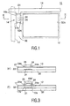
- Fig. 4 is an illustration showing various steps in this second embodiment in a manner similar to Fig. 2 .
- a layer composed of a light-blocking conductive material e.g., a metal such as aluminium
- a transparent substrate 120 made, for example, of glass or quartz with a uniform thickness by sputtering or the like.
- This metal layer is patterned by a known lithography utilizing a first photomask to form gate electrodes 116a and gate lines 116 ( Fig. 5 ) each of which is integral with the gate electrodes 116a (see Fig. 4 at (a)).
- a gate insulating layer 122 composed, for example, of SiO 2 is formed on the entire surface of the substrate 120, on which the gates electrodes 116a and the gate lines 116 have been formed, with a uniform thickness by means of a plasma CVD method or the like.
- a layer of a transparent conductive material such as ITO is then formed on the thus formed gate insulating layer 122 with a uniform thickness, for example, by sputtering.
- This transparent conductive material layer is patterned by a known photolithography utilizing a second photomask, so that pixel electrodes 112, drain electrodes 112a each as a part of the corresponding pixel electrode 112, source lines 117 and source electrodes 117a integral with the corresponding source line 117 are formed (see Fig. 4 at (b)). Then, the structure as obtained in the step shown in Fig. 4 at (b) is doped in its upper surface with phosphorous for the subsequent steps.
- a channel forming layer 124 composed of a semiconductor material such as amorphous silicon (a-Si) and an insulating layer 126 composed of an insulating material such as silicon nitride (SiN x ) are sequentially formed on the entire surface of the above structure, for example, in a plasma CVD method.
- a-Si amorphous silicon
- SiN x silicon nitride
- the doped phosphorous mentioned above diffuses into the portions of the channel forming layer 124 interfacing with the pixel electrodes 112, drain electrodes 112a, source lines 117 and source electrodes 117a, whereby n+a-Si films, for example, are formed therein, which allow good ohmic contacts to be achieved between the channel forming layer 124 and the drain and source electrodes 112a and 117a.
- a photoresist layer 128 is formed on the insulating layer 126. This photoresist layer 128 is exposed to a light from the side of the substrate 120 (i.e., from the rear side) with the gate electrodes 116a and gate lines 116 being used as one mask.
- the photoresist layer 128 is exposed to a light from the upper side in the drawing (i.e., from the front side of the panel) using a third photomask (the other photomask) of a simple configuration which has predetermined light-blocking stripes extending in a direction perpendicular to the length of the gate electrodes 116a (that is to say, in the horizontal direction in Fig. 4 ).
- Fig. 5 schematically illustrates the above-mentioned one and the other masks in a plan view, and shows that the one mask with the gate electrodes 116a and gate lines 116 and the other mask 200 have overlapping areas (cross-hatched areas) which are those regions where the channel forming layers should be formed. More specifically, the other mask 200 should have such a pattern that at least those regions which correspond to the gate electrodes 116a, i.e., the channel forming layers, are not exposed to the light from the top side. In the present example, the mask 200 has a pattern which causes all the regions of the gate lines 116 to be exposed to the light from the top side.
- This pattern can be formed by providing light-transmissive linear stripes 201 which extend along the gate lines 116 to encompass them and light-blocking linear stripes 202 arranged alternately with the stripes 201, and is thus very simple.
- the mask 200 should only be positioned in one direction (i.e., in the vertical direction in Fig. 5 ) and thus contributes to the simplification of the manufacturing steps.
- a protective layer 132 composed of an insulating material such as silicon nitride is formed on the entire surface of the above structure.
- This protective layer 132 is then patterned in a known photolithography utilizing a fourth photomask, so that windows 132a each for exposing a respective one of the pixel electrodes 112 are formed in the protective layer 132 (see Fig. 4 at (e)).
- terminal portions of the gate lines are exposed in a known method. In this manner, TFTs 114 each comprising the drain and source electrodes 112a and 117a, channel forming layer 124, gate insulating layer 122, and gate electrode 116a are obtained.
- the structure as obtained in the step shown in Fig. 4 at (e) is then formed on its entire surface, for example, with an orientation film, but detailed description of such steps will be omitted since they are well known.
- the exposure to light is performed from the rear side with the gate electrodes 116a being used as a photomask, so that when viewed in a direction perpendicular to the substrate 120 each gate electrode 116a and the corresponding channel forming layer 124 agree in shape and position to each other substantially completely, that is to say both layers are self aligned, at least with respect to a pair of opposite sides thereof (the sides 130A and 130B shown in Fig. 5 ; in the present example, the side 130C is also self-aligned).
- the formation of the insulating layer 126 may be omitted and instead only the protective layer 132 may be provided.
- shield layers and the gate electrodes are formed directly on the substrate in the above-described respective embodiments, it goes without saying that these elements may alternatively be formed on an under-coat layer provided on the substrate. Likewise, the invention does not exclude the provision of additional elements in other layers and parts. Also, any modification is possible to the embodiments of the invention as required without departing from the scope of the invention described in the claims.
Landscapes
- Physics & Mathematics (AREA)
- Nonlinear Science (AREA)
- Liquid Crystal (AREA)
- Engineering & Computer Science (AREA)
- Microelectronics & Electronic Packaging (AREA)
- Mathematical Physics (AREA)
- Chemical & Material Sciences (AREA)
- Crystallography & Structural Chemistry (AREA)
- General Physics & Mathematics (AREA)
- Optics & Photonics (AREA)
- Thin Film Transistor (AREA)
Claims (3)
- Verfahren zum Herstellen eines Dünnfilmtransistors, umfassend
ein Substrat (20);
eine Quell- (12a) und eine Drain-Elektrode (17a), die gegenseitig durch einen Kanal (24) getrennt sind, und
eine Gate-Elektrode (16a), die von dem Kanal durch eine Gate-isolierende Schicht (26) isoliert ist, wobei die Gate-Elektrode (16a) auf dem inselförmigen Kanal (24) mit der dazwischen eingefügten Gate-isolierenden Schicht (26) gebildet ist, wobei der Kanal ausgebildet wird, umfassend die Schritte des Aufbringens einer Kanal bildenden Schicht (24) und photolithographischem Mustergeben der Kanal bildenden Schicht (24) mit einer Maske, wobei das Substrat (20) transparent ist und mit der Maske zur Mustergebung der Kanal bildenden Schicht (24) bereitgestellt ist, wobei die Maske eine Abdeckschicht (21) ist, um Licht vor dem Eindringen in den Kanals zu hindern, gekennzeichnet durch Bereitstellen der Quell- (12a) und Drain Elektroden (17a) auf dem Substrat, auf dem die Kanal bildende Schicht aufgebracht wird; Oxidieren von Stirnseiten des Kanals (24), der amorphes Silizium umfasst, und Ausbilden der Gate-Elektrode (16a) auf dem Kanal (24) mit den oxidierten Stirnseiten mit der dazwischen eingefügten Gate-isolierenden Schicht (26). - Verfahren wie in Anspruch 1 beansprucht, dadurch gekennzeichnet, dass das photolithographische Mustergeben die Schritte umfasst:- Bereitstellen einer Photoresistschicht (28) auf der Gate-isolierenden Schicht (26);- Mustergeben der Photoresistschicht (28) basierend auf dem Exponieren von Licht von der Seite des transparenten Substrats (20), wobei die Abdeckschicht (21) als eine Maske verwendet wird; und- selektives Ätzen einer Laminierung der Gate-isolierenden Schicht (26) und der Kanal bildenden Schicht (24) mit der als Maske verwendeten gemusterten Photoresistschicht, dadurch Ausbilden des inselförmigen Kanals (30).
- Verfahren nach Anspruch 1 oder 2, dadurch gekennzeichnet, dass die Oxidation der Stirnseiten der Kanal bildenden Schicht (24) als eine Plasmaoxidationsbehandlung durchgeführt wird.
Applications Claiming Priority (3)
| Application Number | Priority Date | Filing Date | Title |
|---|---|---|---|
| JP2001139552 | 2001-05-10 | ||
| JP2001139552A JP5187994B2 (ja) | 2001-05-10 | 2001-05-10 | 薄膜トランジスタの製造方法並びにそのような製造方法を用いて製造された薄膜トランジスタ及び液晶表示パネル |
| PCT/IB2002/001581 WO2002091455A1 (en) | 2001-05-10 | 2002-05-06 | Thin film transistor self-aligned to a light-shield layer |
Publications (2)
| Publication Number | Publication Date |
|---|---|
| EP1396019A1 EP1396019A1 (de) | 2004-03-10 |
| EP1396019B1 true EP1396019B1 (de) | 2015-07-08 |
Family
ID=18986309
Family Applications (1)
| Application Number | Title | Priority Date | Filing Date |
|---|---|---|---|
| EP02769196.3A Expired - Lifetime EP1396019B1 (de) | 2001-05-10 | 2002-05-06 | Auf eine lichtabschirmschicht selbst-ausgerichteter dünnfilmtransistor |
Country Status (6)
| Country | Link |
|---|---|
| EP (1) | EP1396019B1 (de) |
| JP (1) | JP5187994B2 (de) |
| KR (1) | KR100890745B1 (de) |
| CN (1) | CN1462473A (de) |
| TW (1) | TW569466B (de) |
| WO (1) | WO2002091455A1 (de) |
Families Citing this family (15)
| Publication number | Priority date | Publication date | Assignee | Title |
|---|---|---|---|---|
| JP4141309B2 (ja) * | 2003-04-15 | 2008-08-27 | シャープ株式会社 | 半導体装置およびその製造方法 |
| JP4431081B2 (ja) | 2004-08-30 | 2010-03-10 | エルジー ディスプレイ カンパニー リミテッド | 有機薄膜トランジスタの製造方法及び液晶表示素子の製造方法 |
| KR100623699B1 (ko) * | 2004-09-06 | 2006-09-19 | 삼성에스디아이 주식회사 | 유기 전계 발광 소자 및 그의 제조 방법 |
| KR101090250B1 (ko) * | 2004-10-15 | 2011-12-06 | 삼성전자주식회사 | 유기 반도체를 이용한 박막 트랜지스터 표시판 및 그 제조방법 |
| KR101133767B1 (ko) | 2005-03-09 | 2012-04-09 | 삼성전자주식회사 | 유기 박막 트랜지스터 표시판 및 그 제조 방법 |
| KR20070063300A (ko) * | 2005-12-14 | 2007-06-19 | 삼성전자주식회사 | 유기 박막 트랜지스터 표시판 및 그 제조 방법 |
| CN100389444C (zh) * | 2006-04-24 | 2008-05-21 | 友达光电股份有限公司 | 显示面板模块 |
| KR101248003B1 (ko) | 2006-05-09 | 2013-03-27 | 엘지디스플레이 주식회사 | 액정표시장치용 어레이 기판과 그 제조방법 |
| JP5228298B2 (ja) * | 2006-08-04 | 2013-07-03 | カシオ計算機株式会社 | 半導体薄膜の加工方法及び半導体装置の製造方法 |
| WO2011013417A1 (ja) * | 2009-07-30 | 2011-02-03 | シャープ株式会社 | 薄膜トランジスタおよびその製造方法 |
| KR102012854B1 (ko) * | 2012-11-12 | 2019-10-22 | 엘지디스플레이 주식회사 | 액정표시장치용 어레이기판 및 그 제조방법 |
| KR102424445B1 (ko) | 2016-05-03 | 2022-07-22 | 삼성디스플레이 주식회사 | 박막 트랜지스터 표시판 및 그 제조 방법 |
| CN106298955A (zh) * | 2016-09-07 | 2017-01-04 | 武汉华星光电技术有限公司 | 低温多晶硅薄膜晶体管及其制作方法、液晶面板及显示器 |
| CN111951729B (zh) * | 2020-08-17 | 2023-06-09 | 武汉天马微电子有限公司 | 一种阵列基板、显示面板及显示装置 |
| CN113097227B (zh) * | 2021-03-22 | 2022-10-21 | 北海惠科光电技术有限公司 | 薄膜晶体管、显示装置以及薄膜晶体管制备方法 |
Family Cites Families (18)
| Publication number | Priority date | Publication date | Assignee | Title |
|---|---|---|---|---|
| JPS58170065A (ja) * | 1982-03-31 | 1983-10-06 | Toshiba Corp | 薄膜電界効果トランジスタの製造方法 |
| JPS62291067A (ja) * | 1986-06-10 | 1987-12-17 | Nec Corp | 薄膜トランジスタの製造方法 |
| JPS6446982A (en) * | 1987-08-17 | 1989-02-21 | Casio Computer Co Ltd | Manufacture of thin-film transistor |
| JPH01173650A (ja) * | 1987-12-26 | 1989-07-10 | Seikosha Co Ltd | 非晶質シリコン薄膜トランジスタの製造方法 |
| JPH0687466B2 (ja) * | 1988-07-13 | 1994-11-02 | 株式会社精工舎 | シリコン薄膜トランジスタおよびシリコン薄膜トランジスタの製造方法 |
| JPH02139972A (ja) * | 1988-11-21 | 1990-05-29 | Matsushita Electric Ind Co Ltd | 半導体装置の製造方法 |
| JP2978176B2 (ja) * | 1989-03-23 | 1999-11-15 | 松下電器産業株式会社 | アクティブマトリクス基板の製造方法及び表示装置の製造方法 |
| JPH03116778A (ja) * | 1989-09-28 | 1991-05-17 | Matsushita Electric Ind Co Ltd | アクティブマトリクス基板の製造方法と表示装置の製造方法 |
| JPH03145766A (ja) * | 1989-10-31 | 1991-06-20 | Fujitsu Ltd | 薄膜トランジスタ |
| JP2850564B2 (ja) * | 1991-05-09 | 1999-01-27 | 富士通株式会社 | 薄膜トランジスタマトリックス及びその製造方法 |
| KR940007451B1 (ko) * | 1991-09-06 | 1994-08-18 | 주식회사 금성사 | 박막트랜지스터 제조방법 |
| JPH07162007A (ja) * | 1993-12-10 | 1995-06-23 | Sharp Corp | アクティブマトリクス基板の製造方法 |
| JP3360199B2 (ja) * | 1994-10-06 | 2002-12-24 | 富士通株式会社 | 薄膜トランジスタ・マトリクス基板及びその製造方法 |
| JP3176527B2 (ja) * | 1995-03-30 | 2001-06-18 | シャープ株式会社 | 半導体装置の製造方法 |
| JPH095790A (ja) * | 1995-06-16 | 1997-01-10 | Dainippon Printing Co Ltd | 薄膜トランジスタの製造方法 |
| JPH09246554A (ja) * | 1996-03-04 | 1997-09-19 | Matsushita Electric Ind Co Ltd | 薄膜トランジスタの製造方法および液晶表示装置 |
| JPH10173195A (ja) * | 1996-12-12 | 1998-06-26 | Nec Corp | 薄膜トランジスタ及びその製造方法 |
| GB0021030D0 (en) * | 2000-08-26 | 2000-10-11 | Koninkl Philips Electronics Nv | A method of forming a bottom-gate thin film transistor |
-
2001
- 2001-05-10 JP JP2001139552A patent/JP5187994B2/ja not_active Expired - Fee Related
-
2002
- 2002-05-06 WO PCT/IB2002/001581 patent/WO2002091455A1/en not_active Ceased
- 2002-05-06 KR KR1020037000225A patent/KR100890745B1/ko not_active Expired - Fee Related
- 2002-05-06 EP EP02769196.3A patent/EP1396019B1/de not_active Expired - Lifetime
- 2002-05-06 CN CN02801552A patent/CN1462473A/zh active Pending
- 2002-05-07 TW TW091109452A patent/TW569466B/zh not_active IP Right Cessation
Also Published As
| Publication number | Publication date |
|---|---|
| JP5187994B2 (ja) | 2013-04-24 |
| JP2002343970A (ja) | 2002-11-29 |
| EP1396019A1 (de) | 2004-03-10 |
| KR100890745B1 (ko) | 2009-03-26 |
| TW569466B (en) | 2004-01-01 |
| WO2002091455A1 (en) | 2002-11-14 |
| CN1462473A (zh) | 2003-12-17 |
| KR20030029615A (ko) | 2003-04-14 |
Similar Documents
| Publication | Publication Date | Title |
|---|---|---|
| US7700495B2 (en) | Thin film transistor device and method of manufacturing the same, and liquid crystal display device | |
| JP3503685B2 (ja) | 液晶表示装置及びその製造方法 | |
| KR100540947B1 (ko) | 표시장치와그제조방법 | |
| EP1396019B1 (de) | Auf eine lichtabschirmschicht selbst-ausgerichteter dünnfilmtransistor | |
| US6300174B1 (en) | Liquid crystal panel having a thin film transistor for driver circuit and a method for fabricating thereof | |
| KR20010050055A (ko) | 박막트랜지스터 및 그 제조방법과 그것을 구비한액정표시장치 | |
| US5760861A (en) | Liquid crystal display device and a method for fabricating black matrix thereto | |
| KR100375518B1 (ko) | 액정디스플레이 | |
| KR100309209B1 (ko) | 액정 표시장치 제조방법 및 그 제조방법에 따른 액정표시장치 | |
| US6972219B2 (en) | Thin film transistor self-aligned to a light-shield layer | |
| JP3669082B2 (ja) | 液晶表示素子用薄膜トランジスタアレイ | |
| US20020140877A1 (en) | Thin film transistor for liquid crystal display and method of forming the same | |
| KR101409704B1 (ko) | 액정표시장치 및 그 제조 방법 | |
| JP2002014373A (ja) | 液晶表示装置 | |
| JP3105606B2 (ja) | 液晶装置の製造方法 | |
| JPH1138437A (ja) | 液晶表示装置及びその製造方法 | |
| JP2000196094A (ja) | 薄膜トランジスタ基板および液晶表示装置 | |
| KR100243912B1 (ko) | 액정표시장치 및 그 제조방법 | |
| JP3030751B2 (ja) | 薄膜トランジスタ | |
| JPH07153959A (ja) | 薄膜トランジスタおよびその製法 | |
| KR100205520B1 (ko) | 박막트랜지스터 어레이 기판 및 그 제조방법 | |
| KR101419224B1 (ko) | 액정표시장치용 박막 트랜지스터 어레이 기판 및 그의 제조방법 | |
| KR100192376B1 (ko) | 액정표시장치의 제조방법 | |
| JPH0546933B2 (de) | ||
| KR19980014496A (ko) | 박막트랜지스터의 구조와 그 제조방법 |
Legal Events
| Date | Code | Title | Description |
|---|---|---|---|
| PUAI | Public reference made under article 153(3) epc to a published international application that has entered the european phase |
Free format text: ORIGINAL CODE: 0009012 |
|
| 17P | Request for examination filed |
Effective date: 20031210 |
|
| AK | Designated contracting states |
Kind code of ref document: A1 Designated state(s): AT BE CH CY DE DK ES FI FR GB GR IE IT LI LU MC NL PT SE TR |
|
| RAP1 | Party data changed (applicant data changed or rights of an application transferred) |
Owner name: TPO HONG KONG HOLDING LIMITED |
|
| 17Q | First examination report despatched |
Effective date: 20071213 |
|
| GRAP | Despatch of communication of intention to grant a patent |
Free format text: ORIGINAL CODE: EPIDOSNIGR1 |
|
| INTG | Intention to grant announced |
Effective date: 20150121 |
|
| GRAS | Grant fee paid |
Free format text: ORIGINAL CODE: EPIDOSNIGR3 |
|
| GRAA | (expected) grant |
Free format text: ORIGINAL CODE: 0009210 |
|
| AK | Designated contracting states |
Kind code of ref document: B1 Designated state(s): AT BE CH CY DE DK ES FI FR GB GR IE IT LI LU MC NL PT SE TR |
|
| REG | Reference to a national code |
Ref country code: GB Ref legal event code: FG4D |
|
| REG | Reference to a national code |
Ref country code: AT Ref legal event code: REF Ref document number: 735973 Country of ref document: AT Kind code of ref document: T Effective date: 20150715 Ref country code: CH Ref legal event code: EP |
|
| REG | Reference to a national code |
Ref country code: IE Ref legal event code: FG4D |
|
| REG | Reference to a national code |
Ref country code: DE Ref legal event code: R096 Ref document number: 60247303 Country of ref document: DE |
|
| REG | Reference to a national code |
Ref country code: AT Ref legal event code: MK05 Ref document number: 735973 Country of ref document: AT Kind code of ref document: T Effective date: 20150708 |
|
| REG | Reference to a national code |
Ref country code: NL Ref legal event code: MP Effective date: 20150708 |
|
| PG25 | Lapsed in a contracting state [announced via postgrant information from national office to epo] |
Ref country code: GR Free format text: LAPSE BECAUSE OF FAILURE TO SUBMIT A TRANSLATION OF THE DESCRIPTION OR TO PAY THE FEE WITHIN THE PRESCRIBED TIME-LIMIT Effective date: 20151009 Ref country code: FI Free format text: LAPSE BECAUSE OF FAILURE TO SUBMIT A TRANSLATION OF THE DESCRIPTION OR TO PAY THE FEE WITHIN THE PRESCRIBED TIME-LIMIT Effective date: 20150708 |
|
| PG25 | Lapsed in a contracting state [announced via postgrant information from national office to epo] |
Ref country code: AT Free format text: LAPSE BECAUSE OF FAILURE TO SUBMIT A TRANSLATION OF THE DESCRIPTION OR TO PAY THE FEE WITHIN THE PRESCRIBED TIME-LIMIT Effective date: 20150708 Ref country code: PT Free format text: LAPSE BECAUSE OF FAILURE TO SUBMIT A TRANSLATION OF THE DESCRIPTION OR TO PAY THE FEE WITHIN THE PRESCRIBED TIME-LIMIT Effective date: 20151109 Ref country code: SE Free format text: LAPSE BECAUSE OF FAILURE TO SUBMIT A TRANSLATION OF THE DESCRIPTION OR TO PAY THE FEE WITHIN THE PRESCRIBED TIME-LIMIT Effective date: 20150708 Ref country code: ES Free format text: LAPSE BECAUSE OF FAILURE TO SUBMIT A TRANSLATION OF THE DESCRIPTION OR TO PAY THE FEE WITHIN THE PRESCRIBED TIME-LIMIT Effective date: 20150708 |
|
| REG | Reference to a national code |
Ref country code: DE Ref legal event code: R097 Ref document number: 60247303 Country of ref document: DE |
|
| PG25 | Lapsed in a contracting state [announced via postgrant information from national office to epo] |
Ref country code: DK Free format text: LAPSE BECAUSE OF FAILURE TO SUBMIT A TRANSLATION OF THE DESCRIPTION OR TO PAY THE FEE WITHIN THE PRESCRIBED TIME-LIMIT Effective date: 20150708 Ref country code: IT Free format text: LAPSE BECAUSE OF FAILURE TO SUBMIT A TRANSLATION OF THE DESCRIPTION OR TO PAY THE FEE WITHIN THE PRESCRIBED TIME-LIMIT Effective date: 20150708 |
|
| PLBE | No opposition filed within time limit |
Free format text: ORIGINAL CODE: 0009261 |
|
| STAA | Information on the status of an ep patent application or granted ep patent |
Free format text: STATUS: NO OPPOSITION FILED WITHIN TIME LIMIT |
|
| REG | Reference to a national code |
Ref country code: FR Ref legal event code: PLFP Year of fee payment: 15 |
|
| 26N | No opposition filed |
Effective date: 20160411 |
|
| PGFP | Annual fee paid to national office [announced via postgrant information from national office to epo] |
Ref country code: GB Payment date: 20160527 Year of fee payment: 15 Ref country code: DE Payment date: 20160527 Year of fee payment: 15 |
|
| PG25 | Lapsed in a contracting state [announced via postgrant information from national office to epo] |
Ref country code: BE Free format text: LAPSE BECAUSE OF NON-PAYMENT OF DUE FEES Effective date: 20160531 |
|
| PGFP | Annual fee paid to national office [announced via postgrant information from national office to epo] |
Ref country code: FR Payment date: 20160530 Year of fee payment: 15 |
|
| PG25 | Lapsed in a contracting state [announced via postgrant information from national office to epo] |
Ref country code: BE Free format text: LAPSE BECAUSE OF FAILURE TO SUBMIT A TRANSLATION OF THE DESCRIPTION OR TO PAY THE FEE WITHIN THE PRESCRIBED TIME-LIMIT Effective date: 20150708 Ref country code: LU Free format text: LAPSE BECAUSE OF FAILURE TO SUBMIT A TRANSLATION OF THE DESCRIPTION OR TO PAY THE FEE WITHIN THE PRESCRIBED TIME-LIMIT Effective date: 20160506 |
|
| REG | Reference to a national code |
Ref country code: CH Ref legal event code: PL |
|
| PG25 | Lapsed in a contracting state [announced via postgrant information from national office to epo] |
Ref country code: CH Free format text: LAPSE BECAUSE OF NON-PAYMENT OF DUE FEES Effective date: 20160531 Ref country code: LI Free format text: LAPSE BECAUSE OF NON-PAYMENT OF DUE FEES Effective date: 20160531 |
|
| REG | Reference to a national code |
Ref country code: IE Ref legal event code: MM4A |
|
| PG25 | Lapsed in a contracting state [announced via postgrant information from national office to epo] |
Ref country code: IE Free format text: LAPSE BECAUSE OF NON-PAYMENT OF DUE FEES Effective date: 20160506 |
|
| PG25 | Lapsed in a contracting state [announced via postgrant information from national office to epo] |
Ref country code: NL Free format text: LAPSE BECAUSE OF FAILURE TO SUBMIT A TRANSLATION OF THE DESCRIPTION OR TO PAY THE FEE WITHIN THE PRESCRIBED TIME-LIMIT Effective date: 20150708 |
|
| REG | Reference to a national code |
Ref country code: DE Ref legal event code: R119 Ref document number: 60247303 Country of ref document: DE |
|
| GBPC | Gb: european patent ceased through non-payment of renewal fee |
Effective date: 20170506 |
|
| REG | Reference to a national code |
Ref country code: FR Ref legal event code: ST Effective date: 20180131 |
|
| PG25 | Lapsed in a contracting state [announced via postgrant information from national office to epo] |
Ref country code: GB Free format text: LAPSE BECAUSE OF NON-PAYMENT OF DUE FEES Effective date: 20170506 Ref country code: DE Free format text: LAPSE BECAUSE OF NON-PAYMENT OF DUE FEES Effective date: 20171201 |
|
| PG25 | Lapsed in a contracting state [announced via postgrant information from national office to epo] |
Ref country code: FR Free format text: LAPSE BECAUSE OF NON-PAYMENT OF DUE FEES Effective date: 20170531 Ref country code: CY Free format text: LAPSE BECAUSE OF FAILURE TO SUBMIT A TRANSLATION OF THE DESCRIPTION OR TO PAY THE FEE WITHIN THE PRESCRIBED TIME-LIMIT Effective date: 20150708 |
|
| PG25 | Lapsed in a contracting state [announced via postgrant information from national office to epo] |
Ref country code: TR Free format text: LAPSE BECAUSE OF FAILURE TO SUBMIT A TRANSLATION OF THE DESCRIPTION OR TO PAY THE FEE WITHIN THE PRESCRIBED TIME-LIMIT Effective date: 20150708 Ref country code: MC Free format text: LAPSE BECAUSE OF FAILURE TO SUBMIT A TRANSLATION OF THE DESCRIPTION OR TO PAY THE FEE WITHIN THE PRESCRIBED TIME-LIMIT Effective date: 20150708 |