EP1383014A2 - Pufferspeicher mit zwei Speicherbereichen, Arbeitseinheit und Bilderzeugungsgerät damit; Speichersteuerung zum Überprüfen einer Aktualisierung, Computerprogramm und computerlesbares Speichermedium dafür - Google Patents
Pufferspeicher mit zwei Speicherbereichen, Arbeitseinheit und Bilderzeugungsgerät damit; Speichersteuerung zum Überprüfen einer Aktualisierung, Computerprogramm und computerlesbares Speichermedium dafür Download PDFInfo
- Publication number
- EP1383014A2 EP1383014A2 EP03012796A EP03012796A EP1383014A2 EP 1383014 A2 EP1383014 A2 EP 1383014A2 EP 03012796 A EP03012796 A EP 03012796A EP 03012796 A EP03012796 A EP 03012796A EP 1383014 A2 EP1383014 A2 EP 1383014A2
- Authority
- EP
- European Patent Office
- Prior art keywords
- data
- storage area
- memory
- unit data
- cartridge
- Prior art date
- Legal status (The legal status is an assumption and is not a legal conclusion. Google has not performed a legal analysis and makes no representation as to the accuracy of the status listed.)
- Granted
Links
Images





Classifications
-
- G—PHYSICS
- G06—COMPUTING OR CALCULATING; COUNTING
- G06K—GRAPHICAL DATA READING; PRESENTATION OF DATA; RECORD CARRIERS; HANDLING RECORD CARRIERS
- G06K15/00—Arrangements for producing a permanent visual presentation of the output data, e.g. computer output printers
-
- G—PHYSICS
- G03—PHOTOGRAPHY; CINEMATOGRAPHY; ANALOGOUS TECHNIQUES USING WAVES OTHER THAN OPTICAL WAVES; ELECTROGRAPHY; HOLOGRAPHY
- G03G—ELECTROGRAPHY; ELECTROPHOTOGRAPHY; MAGNETOGRAPHY
- G03G21/00—Arrangements not provided for by groups G03G13/00 - G03G19/00, e.g. cleaning, elimination of residual charge
- G03G21/16—Mechanical means for facilitating the maintenance of the apparatus, e.g. modular arrangements
- G03G21/18—Mechanical means for facilitating the maintenance of the apparatus, e.g. modular arrangements using a processing cartridge, whereby the process cartridge comprises at least two image processing means in a single unit
- G03G21/1875—Mechanical means for facilitating the maintenance of the apparatus, e.g. modular arrangements using a processing cartridge, whereby the process cartridge comprises at least two image processing means in a single unit provided with identifying means or means for storing process- or use parameters, e.g. lifetime of the cartridge
- G03G21/1878—Electronically readable memory
- G03G21/1882—Electronically readable memory details of the communication with memory, e.g. wireless communication, protocols
Definitions
- the data on the memory can be locked when it is determined that rewriting is not to be performed. Even if the data indicates only one of bit-representable 2 statuses, data lock is performed on a predetermined unit of area such as 1 byte (8 bits) according to the internal structure of the memory. That is, since the data size must be expanded to a lockable minimum unit, the efficiency of use of the data areas of the memory is lowered, and wasted data areas occur.
- the order of data storage is as follows.
- an image forming apparatus for forming an image by using a cartridge having a part of elements for image formation, comprising: a memory having a first storage area for storing information related to image formation as predetermined unit data, and a second storage area for storing the information as bit-unit data; and control means for controlling writing/reading of the information related to image formation to/from the memory, wherein the control means stores information corresponding to the predetermined unit data, as the bit-unit data, into the second storage area.
- Fig. 1 is a schematic cross-sectional view showing the structure of a laser printer using the electrophotographic technology to which the present invention is applicable.
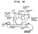
- reference numeral 101 denotesan electrostatic drum as a latent image holder.
- a charging roller 102 which uniformly charges the surface of the electrostatic drum 101 is positioned above the drum in contact with the surface of the drum.
- a light beam 103 is emitted by light emitting means to a position of the charged surface of the electrostatic drum 101 on the downstream side in the rotational direction of the drum from the position in contact with the charging roller 102.
- the unit cartridge 200 is removably attached to the image forming apparatus main body.
- data communication is possible between the EEPROM 219 and the printer controller 204 as shown in Fig. 2.
- communication by connector connection, radio communication or any other communication can be used as long as it enables data transmission/reception with the nonvolatile memory such as an EEPROM.
- Fig. 3B shows data allocation according to the present invention.
- the main buffer 8-byte data area and 1-byte check sum data area are ensured as in the case of allocation in Fig. 3A.
- bit information data
- the backup buffer bit information (data) are handled in bit units, shrunk with other bit information and stored in a 1-byte area.
- the data size including the check sum in the backup buffer is 2 bytes.
- the information indicating the statuses "toner amount: little", “toner amount: zero” (set/reset status) or the like is backed up in bit units, and the information on toner use amount, the information on drum use amount and the like other than the status information are backed up in byte units as in the case of information in the main buffer. That is, as shown in Fig. 3C, the backup buffer in the EEPROM 219 of the process cartridge has a bit-unit backup storage area and a byte-unit backup storage area.
- Fig. 4A shows statuses of the respective buffers and check sum data upon occurrence of abnormality.
- the data areas 1 and 2 have a value indicating the reset status (hereinafter "reset status")
- the data areas 3 and 4 have a value indicating the set status (hereinafter "set status")
- the data areas 5 and 6 have an abnormal value (hereinafter "abnormal value”) not indicating the "set status” nor the “reset status”
- the data areas 7 and 8 have a value indicating the "set status” and these areas are further in a status where the data are locked (hereinbelow "locked status").
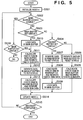
- step S503 if the data area (n) of the main buffer is in the set status, the process proceeds to step S510, at which the data area (n) of the main buffer is changed to the locked status.
- step S511 the check sum in the main buffer is calculated, and the data in the check sum storage area is rewritten.
- step S512 the bit area (n) of the backup buffer is rewritten to the set status.
- step S513 the check sum in the backup buffer is calculated, and data in the check sum storage area is rewritten.
- the developing material is continuously reduced, and if it is determined as "toner amount: zero" when the amount of developing material is equal to or less than a predetermined amount, the data on the memory at the address 00h is still "CAh” indicating the set status, the data at the address 01h becomes “CAh” indicating the set status, the most significant bit at the address 10h as the shrunk information is still "1", and the next most significant bit becomes "1".
- the data at the address 01h is locked, thus rewriting is disabled.
- the data of the memory can be recovered by using the data in the buffer where the check sum corresponds with the calculated value. That is, in the case of double buffer having the above-described structure and the check sum does not correspond with the calculated value in the main buffer, the data recovery is performed in accordance with the following procedure.
- the address 00h data area (1) of the main buffer is in the reset status or shows the abnormal value and the bit information in the bit area (1) of the backup buffer corresponds to the reset status.
- the data in the address 00 data area (1) of the main buffer is rewritten to the reset status (00h)
- the check sum in the main buffer is calculated, and the data in the check sum storage area is rewritten.
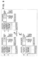
- step S803 if the address 00h data area (1) of the main buffer is in the set status, the process proceeds to step S810, at which the address 00h data area (1) of the main buffer is changed to the locked status.
- step S811 the check sum in the main buffer is calculated, and the data in the check sum storage area is rewritten.
- step S812 the bit area (1) of the backup buffer is rewritten to the set status.
- step S813 the check sum in the backup buffer is calculated, and data in the check sum storage area is rewritten.
- the data area (1) of the main buffer corresponds to the locked status. In this case, it is determined whether or not the address 00h data area (1) of the main buffer is in the set status. If it is not in the set status, it is determined that recovery is impossible (NG).
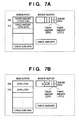
- Figs. 7A and 7B are explanatory views showing processing according to the second embodiment.
- the information, "toner amount: little” and “toner amount: zero” are set at the addresses 00h and 01h corresponding to the main buffer.
- shrunk data “toner amount: little” and “toner amount: zero” are set at address 101h for storing shrunk data corresponding to the backup buffer.
- the data at the address 00h, the address 01h and the shrunk data at the address 10 of the backup buffer are locked, thus rewriting is disabled.
- the program code read from the storage medium realizes the functions according to the embodiments, and the storage medium holding the program code constitutes the invention.
- the present invention includes a case where an OS (operating system) or the like working on the computer performs a part or entire actual processing in accordance with designations of the program code and realizes functions according to the above embodiments.
Landscapes
- Engineering & Computer Science (AREA)
- Physics & Mathematics (AREA)
- General Physics & Mathematics (AREA)
- Computer Networks & Wireless Communication (AREA)
- Computer Vision & Pattern Recognition (AREA)
- General Engineering & Computer Science (AREA)
- Theoretical Computer Science (AREA)
- Control Or Security For Electrophotography (AREA)
- Accessory Devices And Overall Control Thereof (AREA)
- Facsimiles In General (AREA)
Applications Claiming Priority (2)
| Application Number | Priority Date | Filing Date | Title |
|---|---|---|---|
| JP2002167656 | 2002-06-07 | ||
| JP2002167656 | 2002-06-07 |
Publications (3)
| Publication Number | Publication Date |
|---|---|
| EP1383014A2 true EP1383014A2 (de) | 2004-01-21 |
| EP1383014A3 EP1383014A3 (de) | 2004-04-07 |
| EP1383014B1 EP1383014B1 (de) | 2015-03-25 |
Family
ID=29706775
Family Applications (1)
| Application Number | Title | Priority Date | Filing Date |
|---|---|---|---|
| EP03012796.3A Expired - Lifetime EP1383014B1 (de) | 2002-06-07 | 2003-06-05 | Pufferspeicher mit zwei Speicherbereichen, Arbeitseinheit und Bilderzeugungsgerät damit; Speichersteuerung zum Überprüfen einer Aktualisierung, Computerprogramm und computerlesbares Speichermedium dafür |
Country Status (4)
| Country | Link |
|---|---|
| US (2) | US7031622B2 (de) |
| EP (1) | EP1383014B1 (de) |
| KR (1) | KR100514022B1 (de) |
| CN (2) | CN1991634B (de) |
Families Citing this family (6)
| Publication number | Priority date | Publication date | Assignee | Title |
|---|---|---|---|---|
| KR100717011B1 (ko) * | 2005-07-20 | 2007-05-10 | 삼성전자주식회사 | 기입 방지 기능을 이용하여 화상형성장치를 제어하는 방법및 화상형성시스템 |
| JP5171448B2 (ja) * | 2007-07-31 | 2013-03-27 | キヤノン株式会社 | 画像形成装置及びその制御方法 |
| JP4762330B2 (ja) * | 2009-05-27 | 2011-08-31 | シャープ株式会社 | トナーカートリッジ及びトナーカートリッジのトナー残量表示制御方法 |
| CN103064274B (zh) * | 2012-12-03 | 2015-02-04 | 珠海艾派克微电子有限公司 | 成像盒芯片、数据处理方法和成像盒 |
| JP5777649B2 (ja) * | 2013-01-28 | 2015-09-09 | 京セラドキュメントソリューションズ株式会社 | 情報処理装置 |
| JP2024078178A (ja) * | 2022-11-29 | 2024-06-10 | キヤノン株式会社 | 記憶デバイスに格納された情報を更新する更新装置及び画像形成装置 |
Family Cites Families (21)
| Publication number | Priority date | Publication date | Assignee | Title |
|---|---|---|---|---|
| JPS62202294A (ja) * | 1986-02-28 | 1987-09-05 | Casio Comput Co Ltd | カウンタ装置 |
| JPS63106080A (ja) | 1986-06-27 | 1988-05-11 | Hitachi Ltd | 画像表示方式 |
| US5283613A (en) * | 1993-02-19 | 1994-02-01 | Xerox Corporation | Monitoring system with dual memory for electrophotographic printing machines using replaceable cartridges |
| US5778406A (en) * | 1995-06-30 | 1998-07-07 | Thomson Consumer Electronics, Inc. | Apparatus for delivering CPU independent data for little and big endian machines |
| JPH09190137A (ja) * | 1996-01-09 | 1997-07-22 | Canon Inc | プロセスカートリッジ、現像装置及び電子写真画像形成装置 |
| JP3689475B2 (ja) * | 1996-01-09 | 2005-08-31 | キヤノン株式会社 | プロセスカートリッジ、現像装置及び電子写真画像形成装置 |
| JP3248846B2 (ja) * | 1996-07-10 | 2002-01-21 | 株式会社東芝 | 画像形成装置の組立方法 |
| JPH1052964A (ja) * | 1996-08-09 | 1998-02-24 | Canon Inc | 画像形成装置および画像形成装置の消耗材管理方法 |
| JPH1131107A (ja) * | 1997-07-10 | 1999-02-02 | Minolta Co Ltd | メモリのバックアップ方法 |
| JP2000019891A (ja) | 1998-04-27 | 2000-01-21 | Canon Inc | 画像形成装置及びその制御方法、記憶媒体 |
| US6360231B1 (en) | 1999-02-26 | 2002-03-19 | Hewlett-Packard Company | Transactional memory for distributed shared memory multi-processor computer systems |
| JP2000322326A (ja) * | 1999-05-14 | 2000-11-24 | Sharp Corp | バックアップメモリの情報管理方法 |
| JP3777884B2 (ja) * | 1999-07-23 | 2006-05-24 | セイコーエプソン株式会社 | 表示用ドライバic及びそれを用いた電子機器 |
| JP4497689B2 (ja) | 1999-10-01 | 2010-07-07 | キヤノン株式会社 | 印刷装置、交換ユニット、及び、メモリユニット |
| JP2001195313A (ja) * | 2000-01-07 | 2001-07-19 | Canon Inc | バックアップ記憶制御装置、バックアップ記憶制御方法、及び記憶媒体 |
| JP2002023570A (ja) | 2000-07-13 | 2002-01-23 | Canon Inc | 画像形成装置およびその装置ユニット |
| US6549732B2 (en) * | 2000-07-24 | 2003-04-15 | Minolta Co., Ltd. | Processing cartridge for image forming apparatus having a non-volatile memory |
| JP2002067449A (ja) * | 2000-08-31 | 2002-03-05 | Ricoh Co Ltd | バックアップ手段を備えた画像形成装置 |
| JP2002169427A (ja) * | 2000-11-29 | 2002-06-14 | Ricoh Co Ltd | 画像形成装置、画像形成装置用交換部品及び画像形成装置用icチップ |
| US6694106B2 (en) * | 2001-02-19 | 2004-02-17 | Canon Kabushiki Kaisha | Image processing apparatus, a unit used in the apparatus, and a memory device mounted on the unit |
| JP4641356B2 (ja) | 2001-03-09 | 2011-03-02 | キヤノン株式会社 | 画像形成装置 |
-
2003
- 2003-05-28 US US10/446,100 patent/US7031622B2/en not_active Expired - Fee Related
- 2003-06-05 KR KR10-2003-0036237A patent/KR100514022B1/ko not_active Expired - Fee Related
- 2003-06-05 CN CN2007100019949A patent/CN1991634B/zh not_active Expired - Fee Related
- 2003-06-05 CN CNB031371442A patent/CN100524050C/zh not_active Expired - Fee Related
- 2003-06-05 EP EP03012796.3A patent/EP1383014B1/de not_active Expired - Lifetime
-
2005
- 2005-08-11 US US11/201,315 patent/US7050727B2/en not_active Expired - Fee Related
Also Published As
| Publication number | Publication date |
|---|---|
| EP1383014B1 (de) | 2015-03-25 |
| US20030228161A1 (en) | 2003-12-11 |
| US7050727B2 (en) | 2006-05-23 |
| CN1991634A (zh) | 2007-07-04 |
| CN100524050C (zh) | 2009-08-05 |
| US7031622B2 (en) | 2006-04-18 |
| KR20030095291A (ko) | 2003-12-18 |
| CN1470933A (zh) | 2004-01-28 |
| KR100514022B1 (ko) | 2005-09-13 |
| US20060034628A1 (en) | 2006-02-16 |
| EP1383014A3 (de) | 2004-04-07 |
| CN1991634B (zh) | 2010-12-08 |
Similar Documents
| Publication | Publication Date | Title |
|---|---|---|
| KR102169264B1 (ko) | 화상 형성장치, 카트리지 관리 방법, 및 기억매체 | |
| JP4497689B2 (ja) | 印刷装置、交換ユニット、及び、メモリユニット | |
| US6631248B2 (en) | Image forming apparatus with restorable non-volatile memory | |
| JP4679009B2 (ja) | 画像形成装置 | |
| KR20170094517A (ko) | 화상 형성 장치, 그 제어 방법, 컴퓨터 프로그램, 및 카트리지 | |
| JP4641356B2 (ja) | 画像形成装置 | |
| EP1383014B1 (de) | Pufferspeicher mit zwei Speicherbereichen, Arbeitseinheit und Bilderzeugungsgerät damit; Speichersteuerung zum Überprüfen einer Aktualisierung, Computerprogramm und computerlesbares Speichermedium dafür | |
| US7471905B2 (en) | Backup of replaceable device information in an image-forming apparatus | |
| JP4265383B2 (ja) | 画像形成装置及びデータ読み出し書き込み方法 | |
| JP4632396B2 (ja) | メモリ及びメモリの記憶方法 | |
| US6647214B2 (en) | Image forming apparatus and control method therefor | |
| US7133624B2 (en) | Image forming apparatus and program update method in the apparatus | |
| US6970659B2 (en) | Image forming apparatus equipped with detachable process cartridge and control method therefor | |
| JP2004061529A (ja) | 画像形成装置及び画像形成方法 | |
| US20050105925A1 (en) | Method and apparatus to prevent a transfer roller from being contaminated in image forming systems | |
| JP3799087B2 (ja) | 画像形成装置 | |
| KR100334092B1 (ko) | 화상형성장치의용지급지방법 | |
| JPH09114166A (ja) | 画像形成装置 | |
| JP2000019929A (ja) | プロセスカートリッジ及び該プロセスカートリッジを用いた画像形成装置 | |
| US20210255919A1 (en) | Replaceable unit and apparatus to which the replaceable unit is attached | |
| JP2002072786A (ja) | 画像形成装置および画像形成装置の制御方法および記憶媒体 | |
| JP2006195194A (ja) | メモリ書き換え制御装置及び画像記録装置 | |
| JP2002014595A (ja) | 画像形成装置および画像形成方法 | |
| JPH10119394A (ja) | 画像形成装置 | |
| JP2002166609A (ja) | 機能部材およびそれを用いる画像形成装置並びに画像形成方法 |
Legal Events
| Date | Code | Title | Description |
|---|---|---|---|
| PUAI | Public reference made under article 153(3) epc to a published international application that has entered the european phase |
Free format text: ORIGINAL CODE: 0009012 |
|
| AK | Designated contracting states |
Kind code of ref document: A2 Designated state(s): AT BE BG CH CY CZ DE DK EE ES FI FR GB GR HU IE IT LI LU MC NL PT RO SE SI SK TR |
|
| AX | Request for extension of the european patent |
Extension state: AL LT LV MK |
|
| PUAL | Search report despatched |
Free format text: ORIGINAL CODE: 0009013 |
|
| AK | Designated contracting states |
Kind code of ref document: A3 Designated state(s): AT BE BG CH CY CZ DE DK EE ES FI FR GB GR HU IE IT LI LU MC NL PT RO SE SI SK TR |
|
| AX | Request for extension of the european patent |
Extension state: AL LT LV MK |
|
| 17P | Request for examination filed |
Effective date: 20040817 |
|
| AKX | Designation fees paid |
Designated state(s): DE FR GB |
|
| 17Q | First examination report despatched |
Effective date: 20071115 |
|
| GRAJ | Information related to disapproval of communication of intention to grant by the applicant or resumption of examination proceedings by the epo deleted |
Free format text: ORIGINAL CODE: EPIDOSDIGR1 |
|
| GRAP | Despatch of communication of intention to grant a patent |
Free format text: ORIGINAL CODE: EPIDOSNIGR1 |
|
| INTG | Intention to grant announced |
Effective date: 20141008 |
|
| RIN1 | Information on inventor provided before grant (corrected) |
Inventor name: CHIHARA, HIROSHI |
|
| GRAS | Grant fee paid |
Free format text: ORIGINAL CODE: EPIDOSNIGR3 |
|
| GRAA | (expected) grant |
Free format text: ORIGINAL CODE: 0009210 |
|
| AK | Designated contracting states |
Kind code of ref document: B1 Designated state(s): DE FR GB |
|
| REG | Reference to a national code |
Ref country code: GB Ref legal event code: FG4D |
|
| REG | Reference to a national code |
Ref country code: DE Ref legal event code: R096 Ref document number: 60347424 Country of ref document: DE Effective date: 20150507 |
|
| REG | Reference to a national code |
Ref country code: DE Ref legal event code: R097 Ref document number: 60347424 Country of ref document: DE |
|
| PLBE | No opposition filed within time limit |
Free format text: ORIGINAL CODE: 0009261 |
|
| STAA | Information on the status of an ep patent application or granted ep patent |
Free format text: STATUS: NO OPPOSITION FILED WITHIN TIME LIMIT |
|
| 26N | No opposition filed |
Effective date: 20160105 |
|
| REG | Reference to a national code |
Ref country code: FR Ref legal event code: ST Effective date: 20160229 |
|
| PG25 | Lapsed in a contracting state [announced via postgrant information from national office to epo] |
Ref country code: FR Free format text: LAPSE BECAUSE OF NON-PAYMENT OF DUE FEES Effective date: 20150630 |
|
| PGFP | Annual fee paid to national office [announced via postgrant information from national office to epo] |
Ref country code: GB Payment date: 20160627 Year of fee payment: 14 |
|
| PGFP | Annual fee paid to national office [announced via postgrant information from national office to epo] |
Ref country code: DE Payment date: 20160630 Year of fee payment: 14 |
|
| REG | Reference to a national code |
Ref country code: DE Ref legal event code: R119 Ref document number: 60347424 Country of ref document: DE |
|
| GBPC | Gb: european patent ceased through non-payment of renewal fee |
Effective date: 20170605 |
|
| PG25 | Lapsed in a contracting state [announced via postgrant information from national office to epo] |
Ref country code: DE Free format text: LAPSE BECAUSE OF NON-PAYMENT OF DUE FEES Effective date: 20180103 Ref country code: GB Free format text: LAPSE BECAUSE OF NON-PAYMENT OF DUE FEES Effective date: 20170605 |