EP1376673A2 - Semiconductor device manufacturing method - Google Patents
Semiconductor device manufacturing method Download PDFInfo
- Publication number
- EP1376673A2 EP1376673A2 EP03250712A EP03250712A EP1376673A2 EP 1376673 A2 EP1376673 A2 EP 1376673A2 EP 03250712 A EP03250712 A EP 03250712A EP 03250712 A EP03250712 A EP 03250712A EP 1376673 A2 EP1376673 A2 EP 1376673A2
- Authority
- EP
- European Patent Office
- Prior art keywords
- film
- etching
- hard mask
- semiconductor device
- forming
- Prior art date
- Legal status (The legal status is an assumption and is not a legal conclusion. Google has not performed a legal analysis and makes no representation as to the accuracy of the status listed.)
- Withdrawn
Links
- 239000004065 semiconductor Substances 0.000 title claims abstract description 31
- 238000004519 manufacturing process Methods 0.000 title claims abstract description 27
- 238000005530 etching Methods 0.000 claims abstract description 120
- 239000003990 capacitor Substances 0.000 claims abstract description 80
- 239000007789 gas Substances 0.000 claims description 33
- 239000000758 substrate Substances 0.000 claims description 32
- 238000006243 chemical reaction Methods 0.000 claims description 26
- NRTOMJZYCJJWKI-UHFFFAOYSA-N Titanium nitride Chemical compound [Ti]#N NRTOMJZYCJJWKI-UHFFFAOYSA-N 0.000 claims description 14
- QVGXLLKOCUKJST-UHFFFAOYSA-N atomic oxygen Chemical compound [O] QVGXLLKOCUKJST-UHFFFAOYSA-N 0.000 claims description 13
- 239000001301 oxygen Substances 0.000 claims description 13
- 229910052760 oxygen Inorganic materials 0.000 claims description 13
- 239000010936 titanium Substances 0.000 claims description 13
- 239000012298 atmosphere Substances 0.000 claims description 11
- RTAQQCXQSZGOHL-UHFFFAOYSA-N Titanium Chemical compound [Ti] RTAQQCXQSZGOHL-UHFFFAOYSA-N 0.000 claims description 6
- 229910052782 aluminium Inorganic materials 0.000 claims description 6
- XAGFODPZIPBFFR-UHFFFAOYSA-N aluminium Chemical compound [Al] XAGFODPZIPBFFR-UHFFFAOYSA-N 0.000 claims description 6
- 229910052719 titanium Inorganic materials 0.000 claims description 6
- 239000002356 single layer Substances 0.000 claims description 2
- 229910052736 halogen Inorganic materials 0.000 claims 6
- 150000002367 halogens Chemical class 0.000 claims 6
- WKBOTKDWSSQWDR-UHFFFAOYSA-N Bromine atom Chemical compound [Br] WKBOTKDWSSQWDR-UHFFFAOYSA-N 0.000 claims 1
- ZAMOUSCENKQFHK-UHFFFAOYSA-N Chlorine atom Chemical compound [Cl] ZAMOUSCENKQFHK-UHFFFAOYSA-N 0.000 claims 1
- GDTBXPJZTBHREO-UHFFFAOYSA-N bromine Substances BrBr GDTBXPJZTBHREO-UHFFFAOYSA-N 0.000 claims 1
- 229910052794 bromium Inorganic materials 0.000 claims 1
- 229910052801 chlorine Inorganic materials 0.000 claims 1
- 239000000460 chlorine Substances 0.000 claims 1
- 229910052731 fluorine Inorganic materials 0.000 claims 1
- 125000001153 fluoro group Chemical group F* 0.000 claims 1
- 229910052751 metal Inorganic materials 0.000 description 39
- 239000002184 metal Substances 0.000 description 39
- 238000000034 method Methods 0.000 description 29
- 239000011229 interlayer Substances 0.000 description 26
- 229910052814 silicon oxide Inorganic materials 0.000 description 25
- VYPSYNLAJGMNEJ-UHFFFAOYSA-N Silicium dioxide Chemical compound O=[Si]=O VYPSYNLAJGMNEJ-UHFFFAOYSA-N 0.000 description 22
- 239000012535 impurity Substances 0.000 description 16
- 238000009792 diffusion process Methods 0.000 description 13
- ATJFFYVFTNAWJD-UHFFFAOYSA-N Tin Chemical compound [Sn] ATJFFYVFTNAWJD-UHFFFAOYSA-N 0.000 description 12
- XUIMIQQOPSSXEZ-UHFFFAOYSA-N Silicon Chemical compound [Si] XUIMIQQOPSSXEZ-UHFFFAOYSA-N 0.000 description 11
- 239000000463 material Substances 0.000 description 11
- 229910052710 silicon Inorganic materials 0.000 description 11
- 239000010703 silicon Substances 0.000 description 11
- 238000000059 patterning Methods 0.000 description 10
- 230000000694 effects Effects 0.000 description 7
- 238000001020 plasma etching Methods 0.000 description 7
- 238000000137 annealing Methods 0.000 description 6
- 238000002955 isolation Methods 0.000 description 6
- 239000010410 layer Substances 0.000 description 5
- 238000000206 photolithography Methods 0.000 description 5
- 238000005229 chemical vapour deposition Methods 0.000 description 4
- HTXDPTMKBJXEOW-UHFFFAOYSA-N dioxoiridium Chemical compound O=[Ir]=O HTXDPTMKBJXEOW-UHFFFAOYSA-N 0.000 description 4
- 239000003292 glue Substances 0.000 description 4
- 230000003647 oxidation Effects 0.000 description 4
- 238000007254 oxidation reaction Methods 0.000 description 4
- BASFCYQUMIYNBI-UHFFFAOYSA-N platinum Chemical compound [Pt] BASFCYQUMIYNBI-UHFFFAOYSA-N 0.000 description 4
- 239000000126 substance Substances 0.000 description 4
- 229910052581 Si3N4 Inorganic materials 0.000 description 3
- 229910000457 iridium oxide Inorganic materials 0.000 description 3
- MUMZUERVLWJKNR-UHFFFAOYSA-N oxoplatinum Chemical compound [Pt]=O MUMZUERVLWJKNR-UHFFFAOYSA-N 0.000 description 3
- 238000005268 plasma chemical vapour deposition Methods 0.000 description 3
- 229910003446 platinum oxide Inorganic materials 0.000 description 3
- 230000008569 process Effects 0.000 description 3
- 238000004151 rapid thermal annealing Methods 0.000 description 3
- HQVNEWCFYHHQES-UHFFFAOYSA-N silicon nitride Chemical compound N12[Si]34N5[Si]62N3[Si]51N64 HQVNEWCFYHHQES-UHFFFAOYSA-N 0.000 description 3
- QGZKDVFQNNGYKY-UHFFFAOYSA-N Ammonia Chemical compound N QGZKDVFQNNGYKY-UHFFFAOYSA-N 0.000 description 2
- XKRFYHLGVUSROY-UHFFFAOYSA-N Argon Chemical compound [Ar] XKRFYHLGVUSROY-UHFFFAOYSA-N 0.000 description 2
- MYMOFIZGZYHOMD-UHFFFAOYSA-N Dioxygen Chemical compound O=O MYMOFIZGZYHOMD-UHFFFAOYSA-N 0.000 description 2
- MHAJPDPJQMAIIY-UHFFFAOYSA-N Hydrogen peroxide Chemical compound OO MHAJPDPJQMAIIY-UHFFFAOYSA-N 0.000 description 2
- BOTDANWDWHJENH-UHFFFAOYSA-N Tetraethyl orthosilicate Chemical compound CCO[Si](OCC)(OCC)OCC BOTDANWDWHJENH-UHFFFAOYSA-N 0.000 description 2
- 239000006227 byproduct Substances 0.000 description 2
- 229910001882 dioxygen Inorganic materials 0.000 description 2
- -1 for example Substances 0.000 description 2
- 230000006870 function Effects 0.000 description 2
- 238000010438 heat treatment Methods 0.000 description 2
- 230000007246 mechanism Effects 0.000 description 2
- 125000006850 spacer group Chemical group 0.000 description 2
- WQJQOUPTWCFRMM-UHFFFAOYSA-N tungsten disilicide Chemical compound [Si]#[W]#[Si] WQJQOUPTWCFRMM-UHFFFAOYSA-N 0.000 description 2
- 229910021342 tungsten silicide Inorganic materials 0.000 description 2
- 238000001039 wet etching Methods 0.000 description 2
- 229910018182 Al—Cu Inorganic materials 0.000 description 1
- 229910015844 BCl3 Inorganic materials 0.000 description 1
- JFWLFXVBLPDVDZ-UHFFFAOYSA-N [Ru]=O.[Sr] Chemical compound [Ru]=O.[Sr] JFWLFXVBLPDVDZ-UHFFFAOYSA-N 0.000 description 1
- PNEYBMLMFCGWSK-UHFFFAOYSA-N aluminium oxide Inorganic materials [O-2].[O-2].[O-2].[Al+3].[Al+3] PNEYBMLMFCGWSK-UHFFFAOYSA-N 0.000 description 1
- 229910021529 ammonia Inorganic materials 0.000 description 1
- 229910021417 amorphous silicon Inorganic materials 0.000 description 1
- 229910052786 argon Inorganic materials 0.000 description 1
- 239000012300 argon atmosphere Substances 0.000 description 1
- 239000007795 chemical reaction product Substances 0.000 description 1
- 239000011248 coating agent Substances 0.000 description 1
- 238000000576 coating method Methods 0.000 description 1
- 150000001875 compounds Chemical class 0.000 description 1
- 238000001816 cooling Methods 0.000 description 1
- 238000000151 deposition Methods 0.000 description 1
- 230000008021 deposition Effects 0.000 description 1
- 238000001312 dry etching Methods 0.000 description 1
- 238000002474 experimental method Methods 0.000 description 1
- 229910052741 iridium Inorganic materials 0.000 description 1
- GKOZUEZYRPOHIO-UHFFFAOYSA-N iridium atom Chemical compound [Ir] GKOZUEZYRPOHIO-UHFFFAOYSA-N 0.000 description 1
- 229910044991 metal oxide Inorganic materials 0.000 description 1
- 150000004706 metal oxides Chemical class 0.000 description 1
- 238000001000 micrograph Methods 0.000 description 1
- 239000011259 mixed solution Substances 0.000 description 1
- 229910052758 niobium Inorganic materials 0.000 description 1
- 239000012299 nitrogen atmosphere Substances 0.000 description 1
- 230000001590 oxidative effect Effects 0.000 description 1
- 229910052697 platinum Inorganic materials 0.000 description 1
- 238000005498 polishing Methods 0.000 description 1
- 229910021420 polycrystalline silicon Inorganic materials 0.000 description 1
- 229920005591 polysilicon Polymers 0.000 description 1
- 230000009467 reduction Effects 0.000 description 1
- 238000003980 solgel method Methods 0.000 description 1
- 229910052715 tantalum Inorganic materials 0.000 description 1
- FAQYAMRNWDIXMY-UHFFFAOYSA-N trichloroborane Chemical compound ClB(Cl)Cl FAQYAMRNWDIXMY-UHFFFAOYSA-N 0.000 description 1
Images


Classifications
-
- H—ELECTRICITY
- H01—ELECTRIC ELEMENTS
- H01L—SEMICONDUCTOR DEVICES NOT COVERED BY CLASS H10
- H01L27/00—Devices consisting of a plurality of semiconductor or other solid-state components formed in or on a common substrate
- H01L27/02—Devices consisting of a plurality of semiconductor or other solid-state components formed in or on a common substrate including semiconductor components specially adapted for rectifying, oscillating, amplifying or switching and having potential barriers; including integrated passive circuit elements having potential barriers
- H01L27/04—Devices consisting of a plurality of semiconductor or other solid-state components formed in or on a common substrate including semiconductor components specially adapted for rectifying, oscillating, amplifying or switching and having potential barriers; including integrated passive circuit elements having potential barriers the substrate being a semiconductor body
-
- H—ELECTRICITY
- H01—ELECTRIC ELEMENTS
- H01L—SEMICONDUCTOR DEVICES NOT COVERED BY CLASS H10
- H01L28/00—Passive two-terminal components without a potential-jump or surface barrier for integrated circuits; Details thereof; Multistep manufacturing processes therefor
- H01L28/40—Capacitors
- H01L28/55—Capacitors with a dielectric comprising a perovskite structure material
-
- H—ELECTRICITY
- H01—ELECTRIC ELEMENTS
- H01L—SEMICONDUCTOR DEVICES NOT COVERED BY CLASS H10
- H01L21/00—Processes or apparatus adapted for the manufacture or treatment of semiconductor or solid state devices or of parts thereof
- H01L21/02—Manufacture or treatment of semiconductor devices or of parts thereof
- H01L21/04—Manufacture or treatment of semiconductor devices or of parts thereof the devices having potential barriers, e.g. a PN junction, depletion layer or carrier concentration layer
- H01L21/18—Manufacture or treatment of semiconductor devices or of parts thereof the devices having potential barriers, e.g. a PN junction, depletion layer or carrier concentration layer the devices having semiconductor bodies comprising elements of Group IV of the Periodic Table or AIIIBV compounds with or without impurities, e.g. doping materials
- H01L21/30—Treatment of semiconductor bodies using processes or apparatus not provided for in groups H01L21/20 - H01L21/26
- H01L21/31—Treatment of semiconductor bodies using processes or apparatus not provided for in groups H01L21/20 - H01L21/26 to form insulating layers thereon, e.g. for masking or by using photolithographic techniques; After treatment of these layers; Selection of materials for these layers
- H01L21/3105—After-treatment
- H01L21/311—Etching the insulating layers by chemical or physical means
- H01L21/31105—Etching inorganic layers
- H01L21/31111—Etching inorganic layers by chemical means
- H01L21/31116—Etching inorganic layers by chemical means by dry-etching
- H01L21/31122—Etching inorganic layers by chemical means by dry-etching of layers not containing Si, e.g. PZT, Al2O3
-
- H—ELECTRICITY
- H01—ELECTRIC ELEMENTS
- H01L—SEMICONDUCTOR DEVICES NOT COVERED BY CLASS H10
- H01L21/00—Processes or apparatus adapted for the manufacture or treatment of semiconductor or solid state devices or of parts thereof
- H01L21/02—Manufacture or treatment of semiconductor devices or of parts thereof
- H01L21/04—Manufacture or treatment of semiconductor devices or of parts thereof the devices having potential barriers, e.g. a PN junction, depletion layer or carrier concentration layer
- H01L21/18—Manufacture or treatment of semiconductor devices or of parts thereof the devices having potential barriers, e.g. a PN junction, depletion layer or carrier concentration layer the devices having semiconductor bodies comprising elements of Group IV of the Periodic Table or AIIIBV compounds with or without impurities, e.g. doping materials
- H01L21/30—Treatment of semiconductor bodies using processes or apparatus not provided for in groups H01L21/20 - H01L21/26
- H01L21/31—Treatment of semiconductor bodies using processes or apparatus not provided for in groups H01L21/20 - H01L21/26 to form insulating layers thereon, e.g. for masking or by using photolithographic techniques; After treatment of these layers; Selection of materials for these layers
- H01L21/3205—Deposition of non-insulating-, e.g. conductive- or resistive-, layers on insulating layers; After-treatment of these layers
- H01L21/321—After treatment
- H01L21/3213—Physical or chemical etching of the layers, e.g. to produce a patterned layer from a pre-deposited extensive layer
- H01L21/32133—Physical or chemical etching of the layers, e.g. to produce a patterned layer from a pre-deposited extensive layer by chemical means only
- H01L21/32135—Physical or chemical etching of the layers, e.g. to produce a patterned layer from a pre-deposited extensive layer by chemical means only by vapour etching only
- H01L21/32136—Physical or chemical etching of the layers, e.g. to produce a patterned layer from a pre-deposited extensive layer by chemical means only by vapour etching only using plasmas
-
- H—ELECTRICITY
- H01—ELECTRIC ELEMENTS
- H01L—SEMICONDUCTOR DEVICES NOT COVERED BY CLASS H10
- H01L28/00—Passive two-terminal components without a potential-jump or surface barrier for integrated circuits; Details thereof; Multistep manufacturing processes therefor
- H01L28/40—Capacitors
- H01L28/60—Electrodes
-
- H—ELECTRICITY
- H01—ELECTRIC ELEMENTS
- H01L—SEMICONDUCTOR DEVICES NOT COVERED BY CLASS H10
- H01L21/00—Processes or apparatus adapted for the manufacture or treatment of semiconductor or solid state devices or of parts thereof
- H01L21/02—Manufacture or treatment of semiconductor devices or of parts thereof
- H01L21/04—Manufacture or treatment of semiconductor devices or of parts thereof the devices having potential barriers, e.g. a PN junction, depletion layer or carrier concentration layer
- H01L21/18—Manufacture or treatment of semiconductor devices or of parts thereof the devices having potential barriers, e.g. a PN junction, depletion layer or carrier concentration layer the devices having semiconductor bodies comprising elements of Group IV of the Periodic Table or AIIIBV compounds with or without impurities, e.g. doping materials
- H01L21/30—Treatment of semiconductor bodies using processes or apparatus not provided for in groups H01L21/20 - H01L21/26
- H01L21/31—Treatment of semiconductor bodies using processes or apparatus not provided for in groups H01L21/20 - H01L21/26 to form insulating layers thereon, e.g. for masking or by using photolithographic techniques; After treatment of these layers; Selection of materials for these layers
- H01L21/3205—Deposition of non-insulating-, e.g. conductive- or resistive-, layers on insulating layers; After-treatment of these layers
- H01L21/321—After treatment
- H01L21/3213—Physical or chemical etching of the layers, e.g. to produce a patterned layer from a pre-deposited extensive layer
- H01L21/32139—Physical or chemical etching of the layers, e.g. to produce a patterned layer from a pre-deposited extensive layer using masks
Definitions
- the present invention relates to a semiconductor device manufacturing method and, more particularly, a semiconductor device manufacturing method having the step of forming a capacitor that employs a ferroelectric substance.
- FIGS.1A and 1B of the accompanying drawings are explained with reference to FIGS.1A and 1B of the accompanying drawings as follows.
- a first metal film 103, a ferroelectric film 104, and a second metal film 105 are formed sequentially on an insulating film 102 that covers a semiconductor substrate 101, and then a mask 106 having a capacitor planar shape is formed on the second metal film 105.
- regions of the second metal film 105, the ferroelectric film 104, and the first metal film 103, which are not covered with the mask 106, are etched successively. Accordingly, an upper electrode 105a of a capacitor Q o is formed from the second metal film 105 under the mask 106, a dielectric film 104a of the capacitor Q o is formed from the ferroelectric film 104, and a lower electrode 103a of the capacitor Q o is formed from the first metal film 103.
- the method of forming the stacked ferroelectric capacitor is set forth in Patent Application Publication (KOKAI) Hei 8-45905, for example.
- respective planar surfaces of the lower electrode 103a, the dielectric film 104a, and the upper electrode 105a must be set as equal in size as possible by increasing a taper angle ⁇ of a side surface of the capacitor Q o to an upper surface of the insulating film 102 as large as possible.
- the etching by-product which is generated in etching the first metal film 103, the ferroelectric film 104, and the second metal film 105, should be hardly adhered onto the side surfaces of the capacitor Q o .
- the mask must be formed of material with heat resistance.
- a hard mask that is made of a hard film such as a titanium film, a titanium nitride film, an aluminum film, or the like may be considered.
- the first metal film 103, the ferroelectric film 104, and the second metal film 105 are formed sequentially on the insulating film 102. Then, a hard film 110 made of any of titanium, titanium nitride, and aluminum is formed on the second metal film 105. Then, a resist pattern 111 having a capacitor planar shape is formed on the hard film 110.
- the hard film 110 left under the resist pattern 111 is formed into a hard mask 110M by etching the hard film 110 that is exposed from the resist pattern 111.
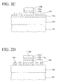
- the resist pattern 111 is removed. Then, as shown in FIGS.2C and 2D, regions of the second metal film 105, the ferroelectric film 104, and the first metal film 103, which are not covered with the hard mask 110M, are etched successively. Accordingly, the capacitor Q o is formed under the hard mask 110M.
- etching resistance of the hard mask 110M is improved extremely by condition of which an oxygen gas is added into the etching gas. Therefore, there is no need to form the hard mask 110M thick.
- the resist pattern 111 used to form the hard mask 110M is made of a resist for excimer exposure, it is indispensable that, in order to enhance the pattern precision, the hard film 110 should be formed thin.
- the etching of the first metal film 103 is carried out in the situation that the residue of PZT is present, the first metal film 103 is left like an island, as shown in FIG.2D, since the residue of the ferroelectric film 104 functions substantially as a mask. As a result, it is possible that the pattern precision of the capacitor Q o is lowered or the upper electrodes 105a of the neighboring capacitors Q o are shortcircuited by the conductive residue.
- the hard mask made of a material that does not cause the microloading effect in etching the ferroelectric film should be employed.
- a material that does not cause the microloading effect in etching the ferroelectric film there are silicon oxide, silicon nitride, etc.
- the silicon oxide film and the silicon nitride film have low etching selectivity to the etching of the first metal film 103, the ferroelectric film 104, and the second metal film 105, the film thickness must be formed thick in excess of 1 ⁇ m.
- Patent Application Publication (KOKAI) 2001-36024 for example, that the hard mask 110M is made of silicon nitride.
- the hard mask having a double-layered structure in which the silicon oxide film is formed on the titanium nitride film may be employed.
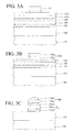
- the first metal film 103, the ferroelectric film 104, and the second metal film 105 are formed sequentially on the insulating film 102. Then, a titanium nitride film 110a and a silicon oxide film 110b are formed on the second metal film 105. Then, a resist pattern 111 having the capacitor planar shape is formed on the silicon oxide film 110b.
- the silicon oxide film 110b and the titanium nitride film 110a exposed from the resist pattern 111 are etched.
- the silicon oxide film 110b and the titanium nitride film flea left under the resist pattern 111 are used as the hard mask 110M.
- the resist pattern 111 is removed. Then, as shown in FIG.3C, regions of the second metal film 105, the ferroelectric film 104, and the first metal film 103, which are not covered with the hard mask 110M, are successively etched. Accordingly, the capacitor Q o is formed under the hard mask 110M.
- the microloading effect is suppressed and thus etching residue of the ferroelectric film 104 is hard to occur, and in addition at least the titanium nitride film 110a is left as the hard mask 110M upon etching the first metal film 103 and thus the gradient of the side surfaces of the capacitor is set steeply.
- the hard mask having the structure shown in FIG.3B when the hard mask having the structure shown in FIG.3B is employed, not only the film forming step of forming the hard mask is increased but also the etching of the silicon oxide film is not suppressed if oxygen is added in etching. Therefore, the silicon oxide film must be formed thick like about 1 ⁇ m, for example. Since it is difficult to pattern such silicon oxide film having a thick film thickness by using a resist for excimer exposure, it is hard to form the hard mask with high precision.
- a semiconductor device manufacturing method including the step that makes it possible to pattern a plurality of films constituting a capacitor with good precision by using hard masks.
- a method of manufacturing a semiconductor device comprising the steps of: forming an insulating film over a semiconductor substrate; forming a first conductive film on the insulating film; forming a ferroelectric film on the first conductive film; forming a second conductive film on the ferroelectric film; forming a hard mask on the second conductive film; forming a capacitor upper electrode under the hard mask by etching the second conductive film in an area, which is exposed from the hard mask, at a first temperature by using a first etching gas; forming a capacitor dielectric film under the hard mask by etching the ferroelectric film in the area, which is exposed from the hard mask, at a second temperature by using a second etching gas; and forming a capacitor lower electrode under the hard mask by etching the first conductive film in the area, which is exposed from the hard mask, at a third temperature that is higher than the second temperature by using a third etching gas.
- the substrate temperature at the time of etching of the ferroelectric film is set lower than the substrate temperature at the time of etching of the first conductive film when the first conductive film constituting the capacitor lower electrode, the ferroelectric film constituting the capacitor dielectric film, and the second conductive film constituting the capacitor upper electrode are etched sequentially by using the same hard mask. More particularly, the substrate temperature at the time of etching of the ferroelectric film is set to below 300 °C, e.g., the atmospheric temperature, whereas the substrate temperature at the time of etching of the first conductive film is set to more than 300 °C.
- the microloading effect is hard to occur because the substrate temperature is lowered when the ferroelectric film is to be etched by using the hard mask, and thus generation of the etching residue of the ferroelectric film is prevented.
- the substrate temperature is set too low, it is possible that the taper angle of the side surface of the capacitor dielectric film becomes small, but the substrate temperature is set high when the first conductive film is to be etched subsequently. Therefore, since side walls of the capacitor dielectric film extruding from the hard mask are also etched at the time of etching of the first conductive film, the taper angle of the side surface of the capacitor dielectric film becomes steep finally.
- the hard mask is formed by material, the etching resistance of which can be improved by adding oxygen into the etching gas, for example, titanium, titanium nitride, or aluminum. Accordingly, the selective etching ratios of the first conductive film, the ferroelectric film, and the second conductive film to the hard mask are enhanced. Therefore, if the hard mask is formed thin, the first conductive film, the ferroelectric film, and the second conductive film are patterned with good precision. In addition, when the hard mask is formed thin, the patterning precision to form the hard mask is improved and also patterning is facilitated.
- the mask forming step does not become complicated and thus reduction in throughput of the mask forming step is prevented.
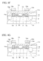
- FIGS.4A to 4K are sectional views showing semiconductor device manufacturing steps according to an embodiment of the present invention.
- an element isolation insulating recess is formed around a transistor forming region of an n-type or p-type silicon (semiconductor) substrate 1 by the photolithography method, and then an element isolation insulating film 2 is formed by burying silicon oxide (SiO 2 ) in the element isolation insulating recess.
- the element isolation insulating film 2 having such a structure is called STI (Shallow Trench Isolation).
- an insulating film formed by the LOCOS (Local Oxidation of Silicon) method may be employed as the element isolation insulating film.
- a p-well 1a is formed by introducing a p-type impurity into the transistor forming region of the silicon substrate 1.
- a silicon oxide film is formed as a gate insulating film 3 by thermally oxidizing a surface of the transistor forming region of the silicon substrate 1.
- gate electrodes 4a, 4b are formed by patterning the silicon film and the tungsten silicide film by virtue of the photolithography method.
- gate electrodes 4a, 4b are formed in parallel over one p-well 1a. These gate electrodes 4a, 4b constitute a part of the word line.
- first to third n-type impurity diffusion regions 5a to 5c serving as the source/drain are formed by ion-implanting an n-type impurity into the p-well 1a on both sides of the gate electrodes 4a, 4b.
- an insulating film e.g., a silicon oxide (SiO 2 ) film is formed on the entire surface of the silicon substrate 1 by the CVD method. Then, insulating sidewall spacers 6 are left on portions on both sides of the gate electrodes 4a, 4b by etching back the insulating film.
- a silicon oxide (SiO 2 ) film is formed on the entire surface of the silicon substrate 1 by the CVD method. Then, insulating sidewall spacers 6 are left on portions on both sides of the gate electrodes 4a, 4b by etching back the insulating film.
- the n-type impurity is ion-implanted into the first to third n-type impurity diffusion regions 5a to 5c once again by using the gate electrodes 4a, 4b and the sidewall spacers 6 as a mask.
- the first to third n-type impurity diffusion regions 5a to 5c are formed as an LDD structure.
- the second n-type impurity diffusion region 5b positioned between two gate electrodes 4a, 4b in one transistor forming region is connected electrically to the bit line, described later.
- the first and third n-type impurity diffusion regions 5a, 5c positioned on both end sides of the transistor forming region are connected electrically to the lower electrode of the capacitor, described later.
- a first MOS transistor T 1 having the gate electrode 4a and the first and second n-type impurity diffusion regions 5a, 5b with the LDD structure and a second MOS transistor T 2 having the gate electrode 4b and the second and third n-type impurity diffusion regions 5b, 5c with the LDD structure are formed on one p-well 1a.
- a silicon oxide nitride (SiON) film of about 200 nm thickness is formed as a cover insulating film 7, which covers the MOS transistors T 1 , T 2 , on the overall surface of the silicon substrate 1 by the plasma CVD method.
- a silicon oxide (SiO 2 ) film of about 1.0 ⁇ m thickness is formed as a first interlayer insulating film 8 on the cover insulating film 7 by the plasma CVD method using the TEOS gas.
- such first interlayer insulating film 8 is annealed at a temperature of 700°C for 30 minutes in an atmospheric-pressure nitrogen atmosphere, for example. Then, an upper surface of the first interlayer insulating film 8 is planarized by the CMP (Chemical Mechanical Polishing) method.
- CMP Chemical Mechanical Polishing
- first and second contact holes 8a, 8b are formed on the first and third n-type impurity diffusion regions 5a, 5c by patterning the cover insulating film 7 and the first interlayer insulating film 8 by virtue of the photolithography method.
- a Ti film of 30 nm thickness and a TiN film of 50 nm thickness are formed sequentially as a glue film on the upper surface of the first interlayer insulating film 8 and in the first and second contact holes 8a, 8b by the sputter method.
- a W film is grown on the TiN film by the CVD method to bury insides of the first and second contact holes 8a, 8b perfectly.
- the W film, the TiN film, and the Ti film are polished by the CMP method to remove them from the upper surface of the first interlayer insulating film 8.
- the W film, the TiN film, and the Ti film left in the first and second contact holes 8a, 8b are used as first and second conductive plugs 11a, 11c, respectively.
- an iridium (Ir) film, a platinum (Pt) film, a platinum oxide (PtO x ) film, an iridium oxide (IrO x ) film, or a strontium ruthenium oxide (SRO) film having a thickness of 300 nm, for example, is formed as a first conductive film 13 on the first and second conductive plugs 11a, 11c and the first interlayer insulating film 8.
- a multi-layered structure film selected from the Ir film, the Pt film, the PtO x film, and the IrO x film may be formed.
- the first interlayer insulating film 8 is annealed to prevent the peeling-off of the film, for example, before or after the first conductive film 13 is formed.
- annealing method RTA (Rapid Thermal Annealing) executed at 600 to 750°C in an argon atmosphere, for example, is employed.
- a PZT film of 100 nm thickness, for example, is formed as a ferroelectric film 14 on the first conductive film 13 by the sputter method.
- the method of forming the ferroelectric film 14 there are the MOD (Metal Organic Deposition) method, the MOCVD (Metal Organic CVD) method, the sol-gel method, etc. in addition to this.
- other PZT material such as PLCSZT, PLZT, etc.
- the Bi-layered structure compound material such as SrBi 2 Ta 2 O 9 , SrBi 2 (Ta, Nb) 2 O 9 , etc., and other metal oxide ferroelectric substance in addition to PZT.
- the ferroelectric film 14 is annealed in an oxygen atmosphere to crystallize.
- a two- step RTA process having the first step executed at a substrate temperature of 600°C for a time of 90 seconds in a mixed gas atmosphere consisting of argon and oxygen, and the second step executed at a substrate temperature of 750°C for a time of 60 seconds in an oxygen atmosphere, for example, is employed.
- an iridium oxide (IrO 2 ) film of 200 nm thickness is formed as a second conductive film 15 on the ferroelectric film 14 by the sputter method.
- a hard film 18 made of titanium nitride is formed on the second conductive film 15 to have a thickness of about 300 nm, for example.
- Material such as titanium, aluminum, or the like, the etching resistance of which is improved by oxygen, as the hard film 18, may be formed in place of the titanium nitride film, otherwise the structure in which these materials are formed as plural layers may be employed.
- resist 16 for excimer laser exposure is coated on the hard film 18, and then the resist 16 is exposed by an excimer laser and then developed.
- the resist 16 is left over the first and second conductive plugs 11a, 11c to have a capacitor planar shape.
- the hard film 18 is etched by using the resist 16 as a mask, and thus the hard film 18 left under the resist 16 is used as a hard mask 18a.
- the etching of the hard film 18 made of titanium nitride is executed by using the inductively coupled (IPC) plasma etching equipment.
- IPC inductively coupled
- the silicon substrate 1 is put on the stage in the reaction chamber, BCl 3 and Cl 2 are introduced into the reaction chamber as the etching gas at flow rates of 40 ml/min. and 60 ml/min. respectively, the source power of 13.56 MHz is set to 250 W, the bias power of 400 kHz is set to 200 W, a degree of vacuum in the reaction chamber is set to 1 Pa, and the stage temperature is set to 25°C.
- the bias power is a power of a high- frequency power supply, which is applied to the antenna coil provided to the top portion of the reaction chamber of the IPC plasma etching equipment.
- the source power is a power of a high-frequency power supply that is connected to the electrostatic chuck fitted to the stage in the reaction chamber.
- the silicon substrate is brought out from the IPC plasma etching equipment and then the resist 16 is removed.
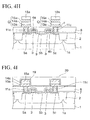
- the second conductive film 15, the ferroelectric film 14, and the first conductive film 13 in the regions that are not covered with the hard mask 18a are etched continuously and sequentially.
- the region of the second conductive film 15, which is exposed from the hard mask 18a, is etched at a high temperature.
- the second conductive film 15 left under the hard mask 18a is used as an upper electrode 15a of the capacitor Q.
- the etching of the second conductive film 15 is carried out by using the IPC plasma etching equipment.
- the etching is carried out by putting the silicon substrate 1 on the stage in the reaction chamber, introducing HBr and O 2 into the reaction chamber as the etching gas at flow rates of 10 ml/min. and 40 ml/min.
- the ferroelectric film 14 left under the hard mask 18a is used as a dielectric film 14a of the capacitor Q.
- the etching of the ferroelectric film 14 may be carried out in the reaction chamber of the same IPC plasma etching equipment as the etching of the second conductive film 15 or may be carried out by using another IPC plasma etching equipment.
- etching conditions for example, Cl 2 , Ar, O 2 and CF 4 are introduced into the reaction chamber as the etching gas at flow rates of 10 ml/min., 40 ml/min., 10 ml/min., and 12 ml/min. respectively, the source power of 13.56 MHz is set to 1400 W, the bias power of 400 kHz is set to 800 W, a degree of vacuum in the reaction chamber is set to 0.7 Pa, and the stage temperature is set within the range from the atmospheric temperature to below 300°C, e.g., 25°C. According to such conditions, generation of residue of the ferroelectric film 14 due to the microloading effect is prevented.
- the region of the first conductive film 13, which is not covered with the hard mask 18a, is etched in the state that the stage temperature is increased higher than that in the etching of the ferroelectric film 14.
- the first conductive film 13 left under the hard mask 18a is used as a lower electrode 13a of the capacitor Q.
- the etching of the first conductive film 13 is carried out in the reaction chamber of the same IPC plasma etching equipment as the etching of the second conductive film 15.
- the etching conditions are given such that, for example, HBr and O 2 are introduced into the reaction chamber as the etching gas at flow rates of 10 ml/min. and 40 ml/min.
- the source power of 13.56 MHz is set to 800 W
- the bias power of 400 kHz is set to 700 W
- a degree of vacuum in the reaction chamber is set to 0.4 Pa
- the stage temperature is set within the range of 300°C to 500°C, e.g., 400°C.
- over-etching is carried out by about 60 % in time.
- a pressure in the atmosphere in which the first conductive film 13 and the second conductive film 15 are etched is set lower than that in the atmosphere in which the ferroelectric film 14 is etched.
- the step of patterning the capacitor Q consisting of the lower electrode 13a, the dielectric film 14a, and the upper electrode 15a is ended.
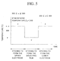
- changes of the substrate temperature in respective etching steps of the second conductive film 15, the ferroelectric film 14, and the first conductive film 13 are shown in FIG.5.
- One lower electrode 13a is connected electrically to the first n-type impurity diffusion region 5a via the first conductive plug 11a over one p-well 1a, while the other lower electrode 13a is connected electrically to the third n-type impurity diffusion region 5c via the second conductive plug 11c. Also, a taper angle ⁇ of the side surfaces of the capacitor Q is about 80 degree.
- the hard mask 18a is removed by wet etching or dry etching.
- a mixed solution consisting of hydrogen peroxide and ammonia, for example, is employed as the etchant of the wet etching applied to the hard mask 18a made of titanium nitride.
- the first interlayer insulating film 8 is etched to remove the silicon oxide and thus a recess is formed in the region between the capacitors Q.
- the hard mask is not formed of the silicon oxide, such problem is not caused.
- recover annealing is executed.
- the recover annealing in this case is executed at a substrate temperature of 650°C for 60 minutes in an oxygen atmosphere, for example.
- alumina of 50 nm thickness is formed as a capacitor protection insulating film 19 on the first interlayer insulating film 8 and the capacitor Q by the sputter. Then, the capacitor Q is annealed at 650°C for 60 minutes in an oxygen atmosphere. The capacitor protection insulating film 19 protects the capacitor Q from the process damage.
- a silicon oxide (SiO 2 ) film of about 1.0 ⁇ m thickness is formed as a second interlayer insulating film 20 on the capacitor protection insulating film 19 by the plasma CVD method using the TEOS gas. Then, an upper surface of the second interlayer insulating film 20 is planarized by the CMP method. In this example, a remaining film thickness of the second interlayer insulating film 20 after CMP is set to about 300 nm on the upper electrode 15a of the capacitor Q.
- the second interlayer insulating film 20, the capacitor protection insulating film 19, and the cover insulating film 7 are etched by using a resist mask (not shown).
- a hole 20a is formed on the second n-type impurity diffusion region 5b.
- a Ti film of 30 nm thickness and a TiN film of 50 nm thickness are formed sequentially as a glue film in the hole 20a and on the second interlayer insulating film 20 by the sputter method. Then, a W film is grown on the glue film by the CVD method to bury perfectly the inside of the hole 20a.
- the W film, the TiN film, and the Ti film are polished by the CMP method to remove them from the upper surface of the second interlayer insulating film 20. Then, the W film and the glue film left in the hole 20a is used as a third conductive plug 21. This third conductive plug 21 is connected electrically to the second n-type impurity diffusion region 5a.
- a SiON film is formed as a second oxidation preventing film (not shown) on the third conductive plug 21 and the second interlayer insulating film 20 by the CVD method. Then, the second oxidation preventing film (not shown), the second interlayer insulating film 20, and the capacitor protection insulating film 19 are patterned by the photolithography method. Thus, contact holes 20b are formed on the upper electrode 15a of the capacitor Q.
- the capacitor Q that is subjected to the damage caused by forming the contact holes 20b is recovered by annealing. This annealing is executed at a temperature of 550°C for 60 minutes in an oxygen atmosphere, for example.
- the oxidation preventing film formed on the second interlayer insulating film 20 is removed by etching-back, and also a surface of the third conductive plug 21 is exposed.
- a metal film is formed in the contact holes 20b on the upper electrodes 15a of the capacitors Q and on the second interlayer insulating film 20.
- first-layer metal wirings 22a which are connected to the upper electrodes 15a via the contact holes 20b, and a conductive pad 22b, which is connected to the third conductive plug 21, are formed by patterning the metal film.
- the layered metal film a multi-layered structure constructed by forming sequentially a Ti film of 60 nm thickness, a TiN film of 30 nm thickness, an Al-Cu film of 400 nm thickness, a Ti film of 5 nm thickness, and a TiN film of 70 nm thickness, for example, is employed.
- the method of patterning the metal film the method of forming a reflection preventing film on the metal film, then coating resist on the reflection preventing film, then forming resist patterns having a wiring shape, etc. by exposing/developing the resist, and then etching the reflection preventing film and the metal film by using the resist patterns is employed.
- a third interlayer insulating film 23 is formed on the second interlayer insulating film 20, the first-layer metal wirings 22a, and the conductive pad 22b. Then, a hole 23a is formed on the conductive pad 22b by patterning the third interlayer insulating film 23. Then, a fourth conductive plug 24 made of a TiN film and a W film sequentially from the bottom is formed in the hole 23a.
- a metal film is formed on the third interlayer insulating film 23.
- a bit line 25 connected to the fourth conductive plug 24 is formed by patterning this metal film by means of the photolithography method.
- the bit line 25 is connected electrically to the second n-type impurity diffusion region 5b via the fourth conductive plug 24, the conductive pad 22b, and the third conductive plug 21.
- an insulating film for covering the second-layer wiring layer, etc. are formed. But their details will be omitted herein.
- the substrate temperature applied to the etching of the second conductive film 15 by using the hard masks 18a is set to a high temperature of more than 300°C but less than 500°C.
- the substrate temperature applied to the etching of the ferroelectric film 14 by using the hard masks 18a is set to a low temperature of more than the atmospheric temperature but below 300°C.
- the substrate temperature applied to the etching of the first conductive film 13 by using the hard masks 18a is set to a high temperature of more than 300°C but less than 500°C.
- the etching resistance of the hard masks 18a can be enhanced and also the selective etching ratios of the films 13, 14, 15 to the hard masks 18a are increased.
- the selective etching ratios of the first conductive film 13 and the second conductive film 15 to the TiN hard masks 18a become infinity, respectively, and thus the hard masks 18a are seldom etched.
- the selective etching ratio of the PZT ferroelectric film 14 to the TiN hard masks 18a becomes about 2, and thus the hard masks 18a are never eliminated at the etching time of the ferroelectric film 14.
- the stage temperature is lowered at the time of etching of the ferroelectric film 14, the microloading effect is difficult to occur and thus the etching residue of the ferroelectric substance is not generated around the capacitors Q.
- FIG.6 is a side view showing a capacitor that was formed actually by forming the hard masks 18a made of TiN and having a thickness of 300 nm on the second conductive film 15, and then patterning the second conductive film 15, the ferroelectric film 14, and the first conductive film 13 under the above etching conditions. As shown in FIG.6, the etching residue shown in FIG.2D has not been generated on the first interlayer insulating film 8 around the capacitors Q.
- FIG.6 is depicted based on a microphotograph that picks up the image of the side surface of the capacitor, which was formed actually under the above etching conditions.
- edge portions of the hard mask 18a are thinner than the center portion thereof since they are etched in etching the ferroelectric film 14.
- the ferroelectric film 14 is etched at a low temperature, a taper angle of the side surface of the dielectric film 14a does not become so steep.
- the side surface of the dielectric film 14a is etched during when the etching of the first conductive film 13 and, in addition, the over-etching of the first conductive film 13, are carried out at a high temperature, respectively.
- the taper angle of the side surface of the capacitor Q containing the side surface of the dielectric film 14a becomes large and sharp.
- the stage temperature used in the etching of the second conductive film 15 is set to 300 to 500°C. But such etching may be carried out at a low temperature in the range of more than the atmospheric temperature but below 300°C. This is because, in the etching of the second conductive film 15, that is, the initial stage of the capacitor Q forming step, the reaction product is hardly adhered onto the side surface of the upper electrode 15a and thus the taper angle of the side surface of the upper electrode 15a becomes large.
- the step of forming the lower electrode 13a since the first conductive film 13 is etched at a high temperature, the portion of the upper electrode 15a extruding from the hard mask 18a is etched simultaneously at that time. Thus, the final taper angle of the side surface of the capacitor Q become steep.
- the etching conditions of the second conductive film 15 when 25°C is selected as the atmospheric temperature are given such that, for example, Cl 2 , Ar, and O 2 are introduced into the reaction chamber as the etching gas at flow rates of 10 ml/min., 40 ml/min., and 10 ml/min. respectively, the source power of 13.56 MHz is set to 1400 W, the bias power of 400 KHz is set to 800 W, and a degree of vacuum in the reaction chamber is set to 0.7 Pa.
- any one of the method of executing the etching in one reaction chamber 31 by executing two types of temperature control, as shown in FIG.7A, and the method of executing the etching by controlling separately the temperatures of wafer stages 41a, 41b in two reaction chambers 41, 42, as shown in FIG.7B, may be employed.
- the wafer stage 32 with a heating/cooling mechanism 33 may be employed or a lamp heating mechanism (not shown) may be provided, in order to implement two types of temperature control.
- the etching equipment in which two reaction chambers 41, 42 or more are connected via a vacuum transferring chamber 43 may be employed or two stand-alone equipments may be employed.
- the substrate temperature at the time of etching the ferroelectric film is set lower than the substrate temperature at the time of etching the first conductive film when the first conductive film constituting the capacitor lower electrode, the ferroelectric film constituting the capacitor dielectric film, and the second conductive film constituting the capacitor upper electrode are to be etched sequentially by using the same hard masks. Therefore, the microloading effect is hard to occur when the ferroelectric film is etched by using the hard masks, and thus generation of the etching residue of the ferroelectric film can be prevented.
Landscapes
- Engineering & Computer Science (AREA)
- Power Engineering (AREA)
- Computer Hardware Design (AREA)
- Microelectronics & Electronic Packaging (AREA)
- Chemical & Material Sciences (AREA)
- Physics & Mathematics (AREA)
- General Physics & Mathematics (AREA)
- Condensed Matter Physics & Semiconductors (AREA)
- Manufacturing & Machinery (AREA)
- General Chemical & Material Sciences (AREA)
- Chemical Kinetics & Catalysis (AREA)
- Inorganic Chemistry (AREA)
- Materials Engineering (AREA)
- Plasma & Fusion (AREA)
- Semiconductor Memories (AREA)
- Drying Of Semiconductors (AREA)
Applications Claiming Priority (2)
| Application Number | Priority Date | Filing Date | Title |
|---|---|---|---|
| JP2002180453A JP2004023078A (ja) | 2002-06-20 | 2002-06-20 | 半導体装置の製造方法 |
| JP2002180453 | 2002-06-20 |
Publications (1)
| Publication Number | Publication Date |
|---|---|
| EP1376673A2 true EP1376673A2 (en) | 2004-01-02 |
Family
ID=29717520
Family Applications (1)
| Application Number | Title | Priority Date | Filing Date |
|---|---|---|---|
| EP03250712A Withdrawn EP1376673A2 (en) | 2002-06-20 | 2003-02-04 | Semiconductor device manufacturing method |
Country Status (5)
| Country | Link |
|---|---|
| US (1) | US20030235944A1 (zh) |
| EP (1) | EP1376673A2 (zh) |
| JP (1) | JP2004023078A (zh) |
| KR (1) | KR20030097640A (zh) |
| TW (1) | TW579543B (zh) |
Families Citing this family (12)
| Publication number | Priority date | Publication date | Assignee | Title |
|---|---|---|---|---|
| JP4551725B2 (ja) * | 2004-09-13 | 2010-09-29 | Okiセミコンダクタ株式会社 | 半導体装置の製造方法 |
| JP2006093451A (ja) * | 2004-09-24 | 2006-04-06 | Toshiba Corp | 半導体装置 |
| JP2007188961A (ja) * | 2006-01-11 | 2007-07-26 | Toshiba Corp | 半導体記憶装置及びその製造方法 |
| JP2007207791A (ja) * | 2006-01-31 | 2007-08-16 | Fujitsu Ltd | 半導体装置の製造方法 |
| JP5028829B2 (ja) * | 2006-03-09 | 2012-09-19 | セイコーエプソン株式会社 | 強誘電体メモリ装置の製造方法 |
| JP4853057B2 (ja) * | 2006-03-09 | 2012-01-11 | セイコーエプソン株式会社 | 強誘電体メモリ装置の製造方法 |
| KR100883139B1 (ko) * | 2007-06-28 | 2009-02-10 | 주식회사 하이닉스반도체 | 루테늄계 전극을 구비한 캐패시터 및 그 제조 방법 |
| JP5245383B2 (ja) * | 2007-12-11 | 2013-07-24 | 富士通セミコンダクター株式会社 | 半導体装置の製造方法 |
| JP4999185B2 (ja) * | 2008-03-04 | 2012-08-15 | 富士フイルム株式会社 | ドライエッチング方法及びドライエッチング装置 |
| JP2009266952A (ja) * | 2008-04-23 | 2009-11-12 | Seiko Epson Corp | デバイスの製造方法及び製造装置 |
| JP6446877B2 (ja) * | 2014-07-16 | 2019-01-09 | Tdk株式会社 | 薄膜キャパシタ |
| KR102593562B1 (ko) * | 2019-02-15 | 2023-10-25 | 삼성전자주식회사 | 재배선 기판, 이의 제조 방법, 및 이를 포함하는 반도체 패키지 |
Family Cites Families (7)
| Publication number | Priority date | Publication date | Assignee | Title |
|---|---|---|---|---|
| JP3122579B2 (ja) * | 1994-07-27 | 2001-01-09 | シャープ株式会社 | Pt膜のエッチング方法 |
| US5563762A (en) * | 1994-11-28 | 1996-10-08 | Northern Telecom Limited | Capacitor for an integrated circuit and method of formation thereof, and a method of adding on-chip capacitors to an integrated circuit |
| JP3024747B2 (ja) * | 1997-03-05 | 2000-03-21 | 日本電気株式会社 | 半導体メモリの製造方法 |
| JPH11220095A (ja) * | 1998-01-30 | 1999-08-10 | Sony Corp | 誘電体キャパシタの製造方法 |
| US6492222B1 (en) * | 1999-12-22 | 2002-12-10 | Texas Instruments Incorporated | Method of dry etching PZT capacitor stack to form high-density ferroelectric memory devices |
| US20030143853A1 (en) * | 2002-01-31 | 2003-07-31 | Celii Francis G. | FeRAM capacitor stack etch |
| JP4014902B2 (ja) * | 2002-03-15 | 2007-11-28 | 富士通株式会社 | 半導体装置の製造方法 |
-
2002
- 2002-06-20 JP JP2002180453A patent/JP2004023078A/ja not_active Withdrawn
-
2003
- 2003-01-29 TW TW092102044A patent/TW579543B/zh not_active IP Right Cessation
- 2003-01-30 US US10/353,943 patent/US20030235944A1/en not_active Abandoned
- 2003-02-04 EP EP03250712A patent/EP1376673A2/en not_active Withdrawn
- 2003-02-22 KR KR10-2003-0011167A patent/KR20030097640A/ko not_active Application Discontinuation
Also Published As
| Publication number | Publication date |
|---|---|
| TW579543B (en) | 2004-03-11 |
| TW200400547A (en) | 2004-01-01 |
| JP2004023078A (ja) | 2004-01-22 |
| US20030235944A1 (en) | 2003-12-25 |
| KR20030097640A (ko) | 2003-12-31 |
Similar Documents
| Publication | Publication Date | Title |
|---|---|---|
| US6825076B2 (en) | Method of manufacturing the FeRAM semiconductor device with improved contact plug structure | |
| US7465657B2 (en) | Method of manufacturing a semiconductor device having a capacitor | |
| US8956881B2 (en) | Method of manufacturing a FeRAM device | |
| US20070114590A1 (en) | Semiconductor device and method of manufacturing the same | |
| US6746878B2 (en) | Semiconductor device and method of manufacturing the same | |
| EP1592046B1 (en) | Semiconductor device manufacturing method | |
| EP1376673A2 (en) | Semiconductor device manufacturing method | |
| US6951788B2 (en) | Method of manufacturing semiconductor device | |
| US6713798B2 (en) | Semiconductor device having a capacitor and method of manufacturing the same | |
| US7763545B2 (en) | Semiconductor device manufacturing method | |
| JP4467891B2 (ja) | 半導体装置の製造方法 | |
| JP2004214544A (ja) | 半導体装置の製造方法 | |
| JP4515492B2 (ja) | 半導体装置の製造方法 | |
| JP2003273323A (ja) | 半導体装置及びその製造方法 | |
| JP2004214456A (ja) | 半導体装置及びその製造方法 |
Legal Events
| Date | Code | Title | Description |
|---|---|---|---|
| PUAI | Public reference made under article 153(3) epc to a published international application that has entered the european phase |
Free format text: ORIGINAL CODE: 0009012 |
|
| AK | Designated contracting states |
Kind code of ref document: A2 Designated state(s): AT BE BG CH CY CZ DE DK EE ES FI FR GB GR HU IE IT LI LU MC NL PT SE SI SK TR |
|
| AX | Request for extension of the european patent |
Extension state: AL LT LV MK RO |
|
| STAA | Information on the status of an ep patent application or granted ep patent |
Free format text: STATUS: THE APPLICATION IS DEEMED TO BE WITHDRAWN |
|
| 18D | Application deemed to be withdrawn |
Effective date: 20060829 |