EP1369910A2 - Montageverfahren für eine Halbleiteranordnung - Google Patents
Montageverfahren für eine Halbleiteranordnung Download PDFInfo
- Publication number
- EP1369910A2 EP1369910A2 EP03016690A EP03016690A EP1369910A2 EP 1369910 A2 EP1369910 A2 EP 1369910A2 EP 03016690 A EP03016690 A EP 03016690A EP 03016690 A EP03016690 A EP 03016690A EP 1369910 A2 EP1369910 A2 EP 1369910A2
- Authority
- EP
- European Patent Office
- Prior art keywords
- head
- adhesive
- chip
- pads
- bumps
- Prior art date
- Legal status (The legal status is an assumption and is not a legal conclusion. Google has not performed a legal analysis and makes no representation as to the accuracy of the status listed.)
- Granted
Links
Images


Classifications
-
- H—ELECTRICITY
- H01—ELECTRIC ELEMENTS
- H01L—SEMICONDUCTOR DEVICES NOT COVERED BY CLASS H10
- H01L24/00—Arrangements for connecting or disconnecting semiconductor or solid-state bodies; Methods or apparatus related thereto
- H01L24/80—Methods for connecting semiconductor or other solid state bodies using means for bonding being attached to, or being formed on, the surface to be connected
- H01L24/81—Methods for connecting semiconductor or other solid state bodies using means for bonding being attached to, or being formed on, the surface to be connected using a bump connector
-
- H—ELECTRICITY
- H01—ELECTRIC ELEMENTS
- H01L—SEMICONDUCTOR DEVICES NOT COVERED BY CLASS H10
- H01L21/00—Processes or apparatus adapted for the manufacture or treatment of semiconductor or solid state devices or of parts thereof
- H01L21/02—Manufacture or treatment of semiconductor devices or of parts thereof
- H01L21/04—Manufacture or treatment of semiconductor devices or of parts thereof the devices having at least one potential-jump barrier or surface barrier, e.g. PN junction, depletion layer or carrier concentration layer
- H01L21/50—Assembly of semiconductor devices using processes or apparatus not provided for in a single one of the subgroups H01L21/06 - H01L21/326, e.g. sealing of a cap to a base of a container
- H01L21/56—Encapsulations, e.g. encapsulation layers, coatings
- H01L21/563—Encapsulation of active face of flip-chip device, e.g. underfilling or underencapsulation of flip-chip, encapsulation preform on chip or mounting substrate
-
- H—ELECTRICITY
- H01—ELECTRIC ELEMENTS
- H01L—SEMICONDUCTOR DEVICES NOT COVERED BY CLASS H10
- H01L24/00—Arrangements for connecting or disconnecting semiconductor or solid-state bodies; Methods or apparatus related thereto
- H01L24/01—Means for bonding being attached to, or being formed on, the surface to be connected, e.g. chip-to-package, die-attach, "first-level" interconnects; Manufacturing methods related thereto
- H01L24/10—Bump connectors ; Manufacturing methods related thereto
- H01L24/11—Manufacturing methods
-
- H—ELECTRICITY
- H01—ELECTRIC ELEMENTS
- H01L—SEMICONDUCTOR DEVICES NOT COVERED BY CLASS H10
- H01L24/00—Arrangements for connecting or disconnecting semiconductor or solid-state bodies; Methods or apparatus related thereto
- H01L24/01—Means for bonding being attached to, or being formed on, the surface to be connected, e.g. chip-to-package, die-attach, "first-level" interconnects; Manufacturing methods related thereto
- H01L24/26—Layer connectors, e.g. plate connectors, solder or adhesive layers; Manufacturing methods related thereto
- H01L24/28—Structure, shape, material or disposition of the layer connectors prior to the connecting process
- H01L24/29—Structure, shape, material or disposition of the layer connectors prior to the connecting process of an individual layer connector
-
- H—ELECTRICITY
- H01—ELECTRIC ELEMENTS
- H01L—SEMICONDUCTOR DEVICES NOT COVERED BY CLASS H10
- H01L24/00—Arrangements for connecting or disconnecting semiconductor or solid-state bodies; Methods or apparatus related thereto
- H01L24/74—Apparatus for manufacturing arrangements for connecting or disconnecting semiconductor or solid-state bodies
- H01L24/75—Apparatus for connecting with bump connectors or layer connectors
-
- H—ELECTRICITY
- H01—ELECTRIC ELEMENTS
- H01L—SEMICONDUCTOR DEVICES NOT COVERED BY CLASS H10
- H01L2224/00—Indexing scheme for arrangements for connecting or disconnecting semiconductor or solid-state bodies and methods related thereto as covered by H01L24/00
- H01L2224/01—Means for bonding being attached to, or being formed on, the surface to be connected, e.g. chip-to-package, die-attach, "first-level" interconnects; Manufacturing methods related thereto
- H01L2224/10—Bump connectors; Manufacturing methods related thereto
- H01L2224/11—Manufacturing methods
- H01L2224/113—Manufacturing methods by local deposition of the material of the bump connector
- H01L2224/1133—Manufacturing methods by local deposition of the material of the bump connector in solid form
- H01L2224/1134—Stud bumping, i.e. using a wire-bonding apparatus
-
- H—ELECTRICITY
- H01—ELECTRIC ELEMENTS
- H01L—SEMICONDUCTOR DEVICES NOT COVERED BY CLASS H10
- H01L2224/00—Indexing scheme for arrangements for connecting or disconnecting semiconductor or solid-state bodies and methods related thereto as covered by H01L24/00
- H01L2224/01—Means for bonding being attached to, or being formed on, the surface to be connected, e.g. chip-to-package, die-attach, "first-level" interconnects; Manufacturing methods related thereto
- H01L2224/10—Bump connectors; Manufacturing methods related thereto
- H01L2224/11—Manufacturing methods
- H01L2224/118—Post-treatment of the bump connector
- H01L2224/1182—Applying permanent coating, e.g. in-situ coating
- H01L2224/11822—Applying permanent coating, e.g. in-situ coating by dipping, e.g. in a solder bath
-
- H—ELECTRICITY
- H01—ELECTRIC ELEMENTS
- H01L—SEMICONDUCTOR DEVICES NOT COVERED BY CLASS H10
- H01L2224/00—Indexing scheme for arrangements for connecting or disconnecting semiconductor or solid-state bodies and methods related thereto as covered by H01L24/00
- H01L2224/01—Means for bonding being attached to, or being formed on, the surface to be connected, e.g. chip-to-package, die-attach, "first-level" interconnects; Manufacturing methods related thereto
- H01L2224/10—Bump connectors; Manufacturing methods related thereto
- H01L2224/12—Structure, shape, material or disposition of the bump connectors prior to the connecting process
- H01L2224/13—Structure, shape, material or disposition of the bump connectors prior to the connecting process of an individual bump connector
- H01L2224/13001—Core members of the bump connector
- H01L2224/13099—Material
- H01L2224/131—Material with a principal constituent of the material being a metal or a metalloid, e.g. boron [B], silicon [Si], germanium [Ge], arsenic [As], antimony [Sb], tellurium [Te] and polonium [Po], and alloys thereof
- H01L2224/13138—Material with a principal constituent of the material being a metal or a metalloid, e.g. boron [B], silicon [Si], germanium [Ge], arsenic [As], antimony [Sb], tellurium [Te] and polonium [Po], and alloys thereof the principal constituent melting at a temperature of greater than or equal to 950°C and less than 1550°C
- H01L2224/13144—Gold [Au] as principal constituent
-
- H—ELECTRICITY
- H01—ELECTRIC ELEMENTS
- H01L—SEMICONDUCTOR DEVICES NOT COVERED BY CLASS H10
- H01L2224/00—Indexing scheme for arrangements for connecting or disconnecting semiconductor or solid-state bodies and methods related thereto as covered by H01L24/00
- H01L2224/01—Means for bonding being attached to, or being formed on, the surface to be connected, e.g. chip-to-package, die-attach, "first-level" interconnects; Manufacturing methods related thereto
- H01L2224/10—Bump connectors; Manufacturing methods related thereto
- H01L2224/15—Structure, shape, material or disposition of the bump connectors after the connecting process
- H01L2224/16—Structure, shape, material or disposition of the bump connectors after the connecting process of an individual bump connector
- H01L2224/161—Disposition
- H01L2224/16151—Disposition the bump connector connecting between a semiconductor or solid-state body and an item not being a semiconductor or solid-state body, e.g. chip-to-substrate, chip-to-passive
- H01L2224/16221—Disposition the bump connector connecting between a semiconductor or solid-state body and an item not being a semiconductor or solid-state body, e.g. chip-to-substrate, chip-to-passive the body and the item being stacked
- H01L2224/16225—Disposition the bump connector connecting between a semiconductor or solid-state body and an item not being a semiconductor or solid-state body, e.g. chip-to-substrate, chip-to-passive the body and the item being stacked the item being non-metallic, e.g. insulating substrate with or without metallisation
-
- H—ELECTRICITY
- H01—ELECTRIC ELEMENTS
- H01L—SEMICONDUCTOR DEVICES NOT COVERED BY CLASS H10
- H01L2224/00—Indexing scheme for arrangements for connecting or disconnecting semiconductor or solid-state bodies and methods related thereto as covered by H01L24/00
- H01L2224/01—Means for bonding being attached to, or being formed on, the surface to be connected, e.g. chip-to-package, die-attach, "first-level" interconnects; Manufacturing methods related thereto
- H01L2224/26—Layer connectors, e.g. plate connectors, solder or adhesive layers; Manufacturing methods related thereto
- H01L2224/31—Structure, shape, material or disposition of the layer connectors after the connecting process
- H01L2224/32—Structure, shape, material or disposition of the layer connectors after the connecting process of an individual layer connector
- H01L2224/321—Disposition
- H01L2224/32151—Disposition the layer connector connecting between a semiconductor or solid-state body and an item not being a semiconductor or solid-state body, e.g. chip-to-substrate, chip-to-passive
- H01L2224/32221—Disposition the layer connector connecting between a semiconductor or solid-state body and an item not being a semiconductor or solid-state body, e.g. chip-to-substrate, chip-to-passive the body and the item being stacked
- H01L2224/32225—Disposition the layer connector connecting between a semiconductor or solid-state body and an item not being a semiconductor or solid-state body, e.g. chip-to-substrate, chip-to-passive the body and the item being stacked the item being non-metallic, e.g. insulating substrate with or without metallisation
-
- H—ELECTRICITY
- H01—ELECTRIC ELEMENTS
- H01L—SEMICONDUCTOR DEVICES NOT COVERED BY CLASS H10
- H01L2224/00—Indexing scheme for arrangements for connecting or disconnecting semiconductor or solid-state bodies and methods related thereto as covered by H01L24/00
- H01L2224/01—Means for bonding being attached to, or being formed on, the surface to be connected, e.g. chip-to-package, die-attach, "first-level" interconnects; Manufacturing methods related thereto
- H01L2224/42—Wire connectors; Manufacturing methods related thereto
- H01L2224/44—Structure, shape, material or disposition of the wire connectors prior to the connecting process
- H01L2224/45—Structure, shape, material or disposition of the wire connectors prior to the connecting process of an individual wire connector
- H01L2224/45001—Core members of the connector
- H01L2224/45099—Material
- H01L2224/451—Material with a principal constituent of the material being a metal or a metalloid, e.g. boron (B), silicon (Si), germanium (Ge), arsenic (As), antimony (Sb), tellurium (Te) and polonium (Po), and alloys thereof
- H01L2224/45138—Material with a principal constituent of the material being a metal or a metalloid, e.g. boron (B), silicon (Si), germanium (Ge), arsenic (As), antimony (Sb), tellurium (Te) and polonium (Po), and alloys thereof the principal constituent melting at a temperature of greater than or equal to 950°C and less than 1550°C
- H01L2224/45144—Gold (Au) as principal constituent
-
- H—ELECTRICITY
- H01—ELECTRIC ELEMENTS
- H01L—SEMICONDUCTOR DEVICES NOT COVERED BY CLASS H10
- H01L2224/00—Indexing scheme for arrangements for connecting or disconnecting semiconductor or solid-state bodies and methods related thereto as covered by H01L24/00
- H01L2224/73—Means for bonding being of different types provided for in two or more of groups H01L2224/10, H01L2224/18, H01L2224/26, H01L2224/34, H01L2224/42, H01L2224/50, H01L2224/63, H01L2224/71
- H01L2224/732—Location after the connecting process
- H01L2224/73201—Location after the connecting process on the same surface
- H01L2224/73203—Bump and layer connectors
- H01L2224/73204—Bump and layer connectors the bump connector being embedded into the layer connector
-
- H—ELECTRICITY
- H01—ELECTRIC ELEMENTS
- H01L—SEMICONDUCTOR DEVICES NOT COVERED BY CLASS H10
- H01L2224/00—Indexing scheme for arrangements for connecting or disconnecting semiconductor or solid-state bodies and methods related thereto as covered by H01L24/00
- H01L2224/74—Apparatus for manufacturing arrangements for connecting or disconnecting semiconductor or solid-state bodies and for methods related thereto
- H01L2224/75—Apparatus for connecting with bump connectors or layer connectors
- H01L2224/7525—Means for applying energy, e.g. heating means
- H01L2224/75251—Means for applying energy, e.g. heating means in the lower part of the bonding apparatus, e.g. in the apparatus chuck
-
- H—ELECTRICITY
- H01—ELECTRIC ELEMENTS
- H01L—SEMICONDUCTOR DEVICES NOT COVERED BY CLASS H10
- H01L2224/00—Indexing scheme for arrangements for connecting or disconnecting semiconductor or solid-state bodies and methods related thereto as covered by H01L24/00
- H01L2224/74—Apparatus for manufacturing arrangements for connecting or disconnecting semiconductor or solid-state bodies and for methods related thereto
- H01L2224/75—Apparatus for connecting with bump connectors or layer connectors
- H01L2224/7525—Means for applying energy, e.g. heating means
- H01L2224/75252—Means for applying energy, e.g. heating means in the upper part of the bonding apparatus, e.g. in the bonding head
-
- H—ELECTRICITY
- H01—ELECTRIC ELEMENTS
- H01L—SEMICONDUCTOR DEVICES NOT COVERED BY CLASS H10
- H01L2224/00—Indexing scheme for arrangements for connecting or disconnecting semiconductor or solid-state bodies and methods related thereto as covered by H01L24/00
- H01L2224/80—Methods for connecting semiconductor or other solid state bodies using means for bonding being attached to, or being formed on, the surface to be connected
- H01L2224/81—Methods for connecting semiconductor or other solid state bodies using means for bonding being attached to, or being formed on, the surface to be connected using a bump connector
- H01L2224/81001—Methods for connecting semiconductor or other solid state bodies using means for bonding being attached to, or being formed on, the surface to be connected using a bump connector involving a temporary auxiliary member not forming part of the bonding apparatus
-
- H—ELECTRICITY
- H01—ELECTRIC ELEMENTS
- H01L—SEMICONDUCTOR DEVICES NOT COVERED BY CLASS H10
- H01L2224/00—Indexing scheme for arrangements for connecting or disconnecting semiconductor or solid-state bodies and methods related thereto as covered by H01L24/00
- H01L2224/80—Methods for connecting semiconductor or other solid state bodies using means for bonding being attached to, or being formed on, the surface to be connected
- H01L2224/81—Methods for connecting semiconductor or other solid state bodies using means for bonding being attached to, or being formed on, the surface to be connected using a bump connector
- H01L2224/812—Applying energy for connecting
- H01L2224/81201—Compression bonding
- H01L2224/81203—Thermocompression bonding, e.g. diffusion bonding, pressure joining, thermocompression welding or solid-state welding
-
- H—ELECTRICITY
- H01—ELECTRIC ELEMENTS
- H01L—SEMICONDUCTOR DEVICES NOT COVERED BY CLASS H10
- H01L2224/00—Indexing scheme for arrangements for connecting or disconnecting semiconductor or solid-state bodies and methods related thereto as covered by H01L24/00
- H01L2224/80—Methods for connecting semiconductor or other solid state bodies using means for bonding being attached to, or being formed on, the surface to be connected
- H01L2224/81—Methods for connecting semiconductor or other solid state bodies using means for bonding being attached to, or being formed on, the surface to be connected using a bump connector
- H01L2224/818—Bonding techniques
- H01L2224/81801—Soldering or alloying
-
- H—ELECTRICITY
- H01—ELECTRIC ELEMENTS
- H01L—SEMICONDUCTOR DEVICES NOT COVERED BY CLASS H10
- H01L2224/00—Indexing scheme for arrangements for connecting or disconnecting semiconductor or solid-state bodies and methods related thereto as covered by H01L24/00
- H01L2224/80—Methods for connecting semiconductor or other solid state bodies using means for bonding being attached to, or being formed on, the surface to be connected
- H01L2224/83—Methods for connecting semiconductor or other solid state bodies using means for bonding being attached to, or being formed on, the surface to be connected using a layer connector
- H01L2224/831—Methods for connecting semiconductor or other solid state bodies using means for bonding being attached to, or being formed on, the surface to be connected using a layer connector the layer connector being supplied to the parts to be connected in the bonding apparatus
- H01L2224/83101—Methods for connecting semiconductor or other solid state bodies using means for bonding being attached to, or being formed on, the surface to be connected using a layer connector the layer connector being supplied to the parts to be connected in the bonding apparatus as prepeg comprising a layer connector, e.g. provided in an insulating plate member
-
- H—ELECTRICITY
- H01—ELECTRIC ELEMENTS
- H01L—SEMICONDUCTOR DEVICES NOT COVERED BY CLASS H10
- H01L2224/00—Indexing scheme for arrangements for connecting or disconnecting semiconductor or solid-state bodies and methods related thereto as covered by H01L24/00
- H01L2224/80—Methods for connecting semiconductor or other solid state bodies using means for bonding being attached to, or being formed on, the surface to be connected
- H01L2224/83—Methods for connecting semiconductor or other solid state bodies using means for bonding being attached to, or being formed on, the surface to be connected using a layer connector
- H01L2224/8319—Arrangement of the layer connectors prior to mounting
- H01L2224/83192—Arrangement of the layer connectors prior to mounting wherein the layer connectors are disposed only on another item or body to be connected to the semiconductor or solid-state body
-
- H—ELECTRICITY
- H01—ELECTRIC ELEMENTS
- H01L—SEMICONDUCTOR DEVICES NOT COVERED BY CLASS H10
- H01L2924/00—Indexing scheme for arrangements or methods for connecting or disconnecting semiconductor or solid-state bodies as covered by H01L24/00
- H01L2924/01—Chemical elements
- H01L2924/01004—Beryllium [Be]
-
- H—ELECTRICITY
- H01—ELECTRIC ELEMENTS
- H01L—SEMICONDUCTOR DEVICES NOT COVERED BY CLASS H10
- H01L2924/00—Indexing scheme for arrangements or methods for connecting or disconnecting semiconductor or solid-state bodies as covered by H01L24/00
- H01L2924/01—Chemical elements
- H01L2924/01005—Boron [B]
-
- H—ELECTRICITY
- H01—ELECTRIC ELEMENTS
- H01L—SEMICONDUCTOR DEVICES NOT COVERED BY CLASS H10
- H01L2924/00—Indexing scheme for arrangements or methods for connecting or disconnecting semiconductor or solid-state bodies as covered by H01L24/00
- H01L2924/01—Chemical elements
- H01L2924/01006—Carbon [C]
-
- H—ELECTRICITY
- H01—ELECTRIC ELEMENTS
- H01L—SEMICONDUCTOR DEVICES NOT COVERED BY CLASS H10
- H01L2924/00—Indexing scheme for arrangements or methods for connecting or disconnecting semiconductor or solid-state bodies as covered by H01L24/00
- H01L2924/01—Chemical elements
- H01L2924/01015—Phosphorus [P]
-
- H—ELECTRICITY
- H01—ELECTRIC ELEMENTS
- H01L—SEMICONDUCTOR DEVICES NOT COVERED BY CLASS H10
- H01L2924/00—Indexing scheme for arrangements or methods for connecting or disconnecting semiconductor or solid-state bodies as covered by H01L24/00
- H01L2924/01—Chemical elements
- H01L2924/01023—Vanadium [V]
-
- H—ELECTRICITY
- H01—ELECTRIC ELEMENTS
- H01L—SEMICONDUCTOR DEVICES NOT COVERED BY CLASS H10
- H01L2924/00—Indexing scheme for arrangements or methods for connecting or disconnecting semiconductor or solid-state bodies as covered by H01L24/00
- H01L2924/01—Chemical elements
- H01L2924/01029—Copper [Cu]
-
- H—ELECTRICITY
- H01—ELECTRIC ELEMENTS
- H01L—SEMICONDUCTOR DEVICES NOT COVERED BY CLASS H10
- H01L2924/00—Indexing scheme for arrangements or methods for connecting or disconnecting semiconductor or solid-state bodies as covered by H01L24/00
- H01L2924/01—Chemical elements
- H01L2924/01033—Arsenic [As]
-
- H—ELECTRICITY
- H01—ELECTRIC ELEMENTS
- H01L—SEMICONDUCTOR DEVICES NOT COVERED BY CLASS H10
- H01L2924/00—Indexing scheme for arrangements or methods for connecting or disconnecting semiconductor or solid-state bodies as covered by H01L24/00
- H01L2924/01—Chemical elements
- H01L2924/01047—Silver [Ag]
-
- H—ELECTRICITY
- H01—ELECTRIC ELEMENTS
- H01L—SEMICONDUCTOR DEVICES NOT COVERED BY CLASS H10
- H01L2924/00—Indexing scheme for arrangements or methods for connecting or disconnecting semiconductor or solid-state bodies as covered by H01L24/00
- H01L2924/01—Chemical elements
- H01L2924/01061—Promethium [Pm]
-
- H—ELECTRICITY
- H01—ELECTRIC ELEMENTS
- H01L—SEMICONDUCTOR DEVICES NOT COVERED BY CLASS H10
- H01L2924/00—Indexing scheme for arrangements or methods for connecting or disconnecting semiconductor or solid-state bodies as covered by H01L24/00
- H01L2924/01—Chemical elements
- H01L2924/01079—Gold [Au]
-
- H—ELECTRICITY
- H01—ELECTRIC ELEMENTS
- H01L—SEMICONDUCTOR DEVICES NOT COVERED BY CLASS H10
- H01L2924/00—Indexing scheme for arrangements or methods for connecting or disconnecting semiconductor or solid-state bodies as covered by H01L24/00
- H01L2924/06—Polymers
- H01L2924/078—Adhesive characteristics other than chemical
- H01L2924/07802—Adhesive characteristics other than chemical not being an ohmic electrical conductor
-
- H—ELECTRICITY
- H01—ELECTRIC ELEMENTS
- H01L—SEMICONDUCTOR DEVICES NOT COVERED BY CLASS H10
- H01L2924/00—Indexing scheme for arrangements or methods for connecting or disconnecting semiconductor or solid-state bodies as covered by H01L24/00
- H01L2924/06—Polymers
- H01L2924/078—Adhesive characteristics other than chemical
- H01L2924/0781—Adhesive characteristics other than chemical being an ohmic electrical conductor
- H01L2924/07811—Extrinsic, i.e. with electrical conductive fillers
Definitions
- the present invention generally relates to a mounting method of a semiconductor device, and more particularly to a method of mounting a semiconductor device on a board in accordance with a COB (Chip On Board) method.
- COB Chip On Board
- a flip-chip mounting method is one of the methods proposed as the COB method.
- a semiconductor device a semiconductor chip
- the flip-chip mounting method is also called a wireless bonding mounting method.
- Pads 2 which are electrodes, are formed on a chip 1 (the semiconductor device) to be mounted on a board 3.
- Pads 4 which are parts of conductive wiring patterns are formed on the board 3 on which the chip 1 is to be mounted.
- bumps are formed as shown in Fig. 1A.
- a gold wire 5 is pressed on a pad 2 of the chip 1 and heated by a boding tool so as to be joined to the pad 2.
- the gold wire 5 is then removed.
- a tear-drop shaped bump 6 is formed on the pad 2.
- tear-drop shaped bumps 6 are formed in the same manner as that describe above.
- the tear-drop shaped bumps 6 are flattened as shown in Fig. 1B.
- the tear-drop shaped bumps 6 are pressed on a flat plate 7 so that only a point end portion of each of the tear-drop shaped bumps 6 is subjected to the plastic deformation.
- the tear-drop shaped bumps 6 are shaped into bumps 6 having substantially the same height.
- Conductive paste is then transferred to a surface of each of the bumps 6 as shown in Figs. 1C and 1D. That is, the end portions of the bumps 6 are immersed in a layer of conductive paste 8 as shown in Fig. 1C and then pulled up therefrom as shown in Fig. 1D. As a result, a drop of the conductive paste 8 is adhered to the end portion of each of the bumps 6.
- the conductive paste 8 is made, for example, of epoxy resin in which a large amount of silver fillers are distributed. Due to the drop of the conductive paste 8, positive electrical conductivity can be maintained between each of the bumps 6 of the chip 1 and a corresponding one of the pads 4 of the board 3 when the chip 1 is mounted on the board 3.
- adhesive 9 is applied toor printed on the surface of the board 3 so that the pads 4 are covered with the adhesive 9 as shown in Fig. 1E.
- a thermosetting insulating adhesive made of material including epoxy resin as the principal ingredient, is used as the adhesive 9 to be applied to the board 3.
- the space between the chip 1 and the board is filled with the adhesive 9.
- the chip 1 and the board 3 are tightly joined to each other.
- a connecting portion in which each of the bumps 6 are joined to a corresponding one of the pads 4 is covered with the adhesive 9, so that moisture is prevented from entering the connection portion by the adhesive 9.
- the chip 1 is mounted on the board 3 as shown in Fig. IF.
- the chip 1 is positioned so that each of the bumps 6 of the chip 1 corresponds to one of the pads 4 of the board 3.
- a thermopressing head then presses the chip 1 on the board 3, so that each of the bumps 6 is pressed on a corresponding one of the pads 4 of the board 3.
- the adhesive 9 and the conductive paste 8 are thus hardened by the heat, so that the chip 1 is completely mounted on the board 3.
- the board on which semiconductor devices are mounted is set and used in electronic equipment, such as a personal computer. Due to the heat generated by the semiconductor devices on the board, the interior of such electronic equipment is at a high temperature. Particularly, in a case where a processor operated at a high frequency is included in the semiconductor device, a large amount of heat is generated. On the other hand, in a case where the electronic equipment is not used, that is, a power supply of the electronic equipment is in an off-state, the interior temperature of the electronic equipment decreases to a room temperature.
- the interior temperature variation of the electronic equipment affects the connecting portion in which each of the semiconductor devices and the board are connected to each other as follows.
- the adhesive 9 between the semiconductor device 1 (the chip) and the board 3 is thermally expanded and contracted, so that the volume of the adhesive 9 is varies.
- thermal expansion and contraction occurs in the board 3, the semiconductor device 1 and the bumps 6.
- the rate of expansion (contraction) thereof is less than that of expansion of the adhesive 9.
- the volume of the adhesive 9 is increased an the increase of the volume of the adhesive 9 functions as a force to increase the distance between the board 3 and the semiconductor device.
- a contact force of the bumps 6 to the pads 4 of the board 3 is decreased, so hat an electric contact resistance between each of the bumps 6 and a corresponding one of the pads 4 is increased.
- the electrical contact resistance is successively increased and finally a disconnection may occur between the bumps 6 and the pads 4.
- Document WO-A-96/05614 discloses a method of mounting a semiconductor device having bumps on a board having pads so that each of the bumps is joined to a corresponding one of the pads, an insulating adhesive to be hardened by heat being provided between the semiconductor device and the board, and the method may be considered to comprise the steps of: (a) pressing the bumps of the semiconductor device on the pads of the board; and (b) heating a portion in which each of the bumps and a corresponding one of the pads are in contact with each other, wherein pressure of the bumps against the pads reaches a predetermined value before a temperature of the insulating adhesive to which heat is supplied in step (b) reaches a temperature at which the insulating adhesive is hardened.
- This document relates to a flip-chip technology using non-conductive adhesives and gold ball bumps or connectors. Bare chips with gold ball bumps are simultaneously attached and interconnected to organic substrates. The chip is fixed by cooling the insulative adhesive.
- a general object of the present invention is to provide a novel and useful mounting method of a semiconductor device in which the disadvantages of the aforementioned prior art are eliminated.
- a specific object of the present invention is to provide a method of mounting a semiconductor device on a board so that even if the volume of adhesive between the semiconductor device and the board is varied by the variation of temperature, an increase of the electrical contact resistance of the semiconductor device to the board can be prevented.
- a Method of mounting a semiconductor device on a board according to the present invention is characterized in that:
- the bumps are pressed on the pads with a pressing force of a predetermined value before the adhesive is completely hardened, the bumps can be securely joined to the pads so as to provide a sufficient contact area.
- the hardened adhesive is expanded and contracted by the variation of temperature, the electrical contact between the bumps and the pads can be maintained.
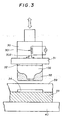
- a chip 31 (the semiconductor device to be mounted) is supported by a thermopressing head 30.
- the chip 31 is mounted on a board 33 by an operation of the thermopressing head 30.
- the thermopressing head 30 is movable in directions indicated by arrows in Fig. 3 and provided with a heater 301 and a vacuum cavity 302.
- the heater 301 is supplied with an electric current from a power supply.
- the heater 301 generates an amount of heat sufficient to warm up adhesive 39 (which will be described later) to a temperature needed to harden the adhesive 39.
- the vacuum cavity 302 is connected to a vacuum system (not shown) so as to support the chip 31 by a suction force of the vacuum.
- a bump 36 made of gold (Au) is formed on a pad 32 of the chip 31.
- the bump 36 has a bowl-shaped root portion and an end portion.
- the conductive paste 38 is then transferred to or printed on the surface of the flattened end portion of the bump 36.
- the conductive paste 38 is made of a thermosetting resin, such as the epoxy resin, in which silver (Ag) fillers are distributed. The conductive paste 38 transferred to the flattened end portion of the bump 36 is preheated so as to be in a semi-hardened state.
- the surface of the chip 31 opposite to the surface on which a circuit is formed is held in position by the vacuum cavity 301, so that the chip 31 is supported by the thermopressing head 30.
- the board 33 is positioned and fixed on a table 40.
- a pad 34 which should be electrically connected to the bump 36 is formed on the board 33.
- the pad 34 is generally made of copper (Cu).
- the adhesive 39 is applied to the surface of the board by using a dispenser or a printing technique.
- the adhesive 39 is made of thermosetting insulating resin including epoxy resin as the principal ingredient.
- the adhesive 39 has a heating characteristic by which liquidity of the adhesive is produced by an initial heating stage and then is gradually hardened with increasing temperature.
- liquidity of the adhesive 39 applied to the whole surface of the board 33 is temporarily produced when the chip 32 is pressed on the board 33 by the thermopressing head 30, the adhesive 39 is prevented from flowing between the bump 36 of the chip 32 and the pad 34 of the board 33.
- the adhesive 39 may be applied to the surface of the board 33, except for the pad 34, by using the printing technique.
- Fig. 4 is a timing chart indicating a time variation of the temperature and pressure in a thermopressing step.
- the axis of the abscissa indicates the time t and the axis of ordinate indicates the temperature T and the pressure P.
- thermopressing head 30 In a state where the chip 32 is set in the thermopressing head 30, the thermopressing head 30 start to go down toward the table 40. The chip 32 is pressed on the board 33 by the thermopressing head 30. While the thermopressing head 30 is going down, the contact pressure PP of the bump 36 of the chip 32 to the pad 34 of the board is gradually increased from a time t 0 .
- the temperature TT of the adhesive 39 is gradually increased from room temperature RT. The reason is that the thermopressing head 30 is preheated by the heater 301 at a temperature sufficient to harden the adhesive 39.
- thermopressing head 30 While the thermopressing head 30 is moving further down, the contact pressure PP and the temperature TT of the adhesive 39 are increased.
- the thermopressing head 30 stops movement at a time t 1 and is maintained at the position.
- the contact pressure PP of the bump 36 to the pad 34 is maintained at a value PA shown in Fig. 5.
- Fig. 5 shows a relationship between the contact pressure P and the electrical contact resistance R between the gold (Au) and the copper (Cu).
- the electrical contact resistance is large. This region means that the connection between the gold and the copper is inferior.
- the contact pressure P is increased and reaches a value equal to or greater than P1, the electrical contact resistance rapidly decreases. This state means that the connection between the gold and the copper is favorable.
- the value PA at which the contact pressure PP of the bump 36 to the pad 34 should be controlled is set so as to be greater than the value P1.
- the value PA is set at 30 grams.
- the value PA of the contact pressure PP is a value sufficient to provide plastic deformation to not only the end portion of the bump 36 but also the root portion of the bump 36.
- the pad 34 of the board 33 is subjected to plastic deformation by the bump 36.
- the temperature TT of the adhesive 39 does not reach a hardening temperature HT at which the adhesive 39 should be hardened.
- the adhesive 39 starts to be heated at the hardening temperature HT.
- the adhesive 39 is gradually hardened. From the time t 3 , the adhesive 39 is heated at the hardening temperature HT so as to be rapidly hardened.
- a time needed to completely harden the adhesive 39 depends on ingredients of the adhesive 39 and is, for example, within a range between 15 seconds and 20 seconds.
- thermopressing head 30 maintains the bump 36 in a state in which it is pressed on the pad 34 with a contact pressure PP of the value PA.
- the vacuum cavity 302 of the thermopressing head 30 is returned to atmospheric pressure so that the chip 32 is released from being supported by the thermopressing head 30.
- the thermopressing head 30 then starts to go up. Since the adhesive 39 is released from being heated by the thermopressing head 30, the temperature of the adhesive 39 is gradually decreased to the room temperature RT.
- the volume of the adhesive 39 is decreased, that is, the adhesive 39 is contracted.
- the contact pressure is temporarily decreased immediately after the head 30 goes up and is separated from the chip 31.
- a tension force is generated between the chip 31 and the board 33.
- the pressure force of the bump 36 to the pad 34 returns to and can be maintained at the initial value PA.
- thermopressing head 30 from which the chip 32 has been separated is maintained at the hardening temperature of the adhesive.
- the next chip is then supported on the thermopressing head 30 by the vacuum suction force.
- the conductive paste 38 covering the surface of the bump 36 is made of resin in which silver fillers are distributed.
- the conductive paste 38 may be made of anisotropic conductive adhesive in which capsules are distributed, each of the capsules being formed by covering silver articles with resin. In this case, the cover of each of the capsules is broken when the bump is pressed on the pad. The silver articles being positioned between the bump and the pad.
- the electrical connection between the bump 36 and the pad mainly depends on the direct contact of the bump 36 with the pad.
- the conductive paste 38 is additionally used for the electrical connection between the bump 36 and the pad.
- the conductive paste 38 is not necessarily needed.
- the bump 38 may have a shape (e.g., a cylindrical shape) other than a shape having the bowl-shaped root portion and the end portion as described above.
- the adhesive 39 may be heated by a heater provided near the table, as a substitute for the heater 301 mounted in the thermopressing head.
- the adhesive 39 is previously applied to the board 33. After the bump 36 is pressed on the pad, the adhesive 39 may be put into the space between the chip and the board. However, it is preferable that the adhesive 39 is previously applied to the board 33 before the bump 39 is pressed on the pad as described in the above embodiment.
- a chip mounting machine 50 as shown in Fig. 6 is used to mount a chip on a board.
- the chip mounting machine 50 has a head 30A, a raising and lowering mechanism 52, a table 40, a transferring mechanism 53 and a head supporting mechanism 54.
- the raising and lowering mechanism 52 is mounted on a gate-shaped block 51 and causes the head 30A to reciprocate up and down.
- the head supporting mechanism 54 supports the head 30A.
- a heater 61 and a thermocouple 62 are mounted in a head body 61 of the head 30A.
- the head 30A is heated at 170°C which is the hardening temperature of the adhesive 39.
- the transferring mechanism 53 has reel supporting blocks 70 and 71 installed at both sides of the gate-shaped block 51, reels 72 and 73 rotatably supported by the reel supporting blocks 70 and 71, motors 74 and 75 rotating the reels 73 and 74, and a polyimide film sheet 76.
- the polyimide film sheet 76 is wound on the reels 72 and 73 from both sides thereof so as to cross the gate-shaped block 51.
- a stainless steel plate 80 which is used as a jig is transferred by a conveyer and set on the table 40A.
- the polyimide film sheet 76 is located at a position (H1) slightly higher than the stainless steel plate 80 set on the table 40A.
- the polyimide film sheet 76 is transferred in a direction A by rotation of each of the reels 72 and 73 respectively driven by the motors 74 and 75.
- the polyimide film sheet 76 has a relatively low thermal conductivity, such as 12 °C/cm.
- the thickness of the polyimide film sheet 76 is 25 ⁇ m.
- a heater 95 is mounted in the table 40A, so that the table 40A is heated at 80°C.
- the raising and lowering mechanism 52 causes a guide 55 of a head supporting mechanism 54 to go up and down (vertically reciprocate).
- the chip 10 is provisionally mounted on a flexible printed circuit board 81 which is fixed on the stainless steel plate 80, using a chip provisional mounting machine (not shown).
- a semi-finished product 90 in which the chip 10 is provisionally mounted is formed.
- the semi-finished product 90 is transferred to the chip mounting machine 50 by the conveyer and set therein.
- the head 30A presses the chip 10 on the flexible printed circuit board 81, with heat, so that the chip 10 is completely mounted on the flexible printed circuit board 81.
- Fig. 6 shows a state in which the semi-finished product 90 transferred into the chip mounting machine 50 is positioned and set on the table 40A.
- the polyimide film sheet 76 is slightly over the chip 10.
- the raising and lowering mechanism 52 is operated so that the head 30A moves downwardly.
- the head 30A presses the chip 10 on the flexible circuit board 81 with application of heat.
- the polyimide film sheet 76 is set. After a predetermined time has elapsed, the head 30A is caused to move upwardly and separate from the chip 10.
- the pressing characteristic of the head 30A pressing the chip 10 is indicated by a line I in Fig. 8. That is, the pressure of the head 30A to the chip 10 is gradually increased starting from a time t 10 as indicated by a line Ia and reaches a value PAa at a time t 12 . After this, the pressure is maintained at the value PAa as indicated by a line Ib and is gradually decreased starting from a time t 14 as indicated by a line Ic.
- the time t 14 is a time at which a time period T1 that is needed to completely harden the adhesive 39 elapses from a time t 13 at which the temperature of the adhesive 39 reaches the hardening temperature of 170°C.
- the adhesive 39 is heated via the chip 10 until the temperature of the adhesive 39 reaches the hardening temperature of 170°C.
- the temperature of the adhesive 39 varies as indicated by a line II in Fig. 8.
- the temperature of the adhesive 39 is rapidly increased as indicated by a line IIa in Fig. 8.
- a time period T2 between the time t 10 at which the head 30A is brought into contact with the chip 10 and a time 11 at which the temperature of the adhesive 39 reaches the hardening temperature of 170°C is relatively short.
- the time t 12 at which the pressure of the head 30A to the chip 10 reaches the predetermined value PAa is after the time t 11 . That is, before the pressure of the head 30A to the chip 10 reaches the predetermined value PAa, the adhesive starts to be hardened.
- some of the bumps 36 may be incompletely joined to the pads.
- the heat is transmitted through the polyimide film sheet 76 having a low thermal conductivity to the adhesive 39.
- the temperature of the adhesive 39 is increased, starting from the time t 10 at which the head 30A starts to press the chip 10, to the hardening temperature of 170°C as indicated by a line IIb.
- the line IIb is more gently sloping than the line IIa.
- a time period T3 between the time t 10 at which the head 30A starts to press the chip 10 and the time t 13 at which the temperature of the adhesive 39 reaches the hardening temperature of 170°C is greater than the time period T2 described above by T4.
- the pressure of the head 30A to the chip 10 reaches the predetermined value PAa at the time t 12 , before the time t 13 . That is, before the adhesive 30 starts to be hardened, the pressure of the head 30A to the chip 10 reaches the predetermined value PAa. After the pressure reaches the predetermined value, the adhesive 39 starts to harden. As a result, the bump 36 is appropriately pressed on the pad so as to be securely joined to the pad. Thus, the chip 10 can be mounted on the board with a high reliability.
- a line IIc indicates an increasing characteristic of the temperature of the adhesive 39 when the semi-finished product 90 is set on and heated by the table 40A.
- the polyimide film sheet 76 Since the polyimide film sheet 76 has a heat resistance property, the polyimide film sheet 76 does not adhere to the head 30A and chip 10. The polyimide film sheet 76 is flexible, so that the surface of the chip 10 is not damaged.
- the motors 73 and 74 are driven so that the polyimide film sheet 76 is moved by one step.
- a part of the polyimide film sheet 76 which was set between the head 30A and the chip 10 is moved to the outside of the gate-shaped block 51 and a new part of the polyimide film sheet 76 which has not yet been used is fed into a space in the gate-shaped block 51.
- the new part of the polyimide film sheet 76 is used for the next semi-finished product 90 so as to be set between the head 30A and the chip 10.
- a polyester film sheet or a silicon film sheet may be substituted for the polyimide film sheet 76.
- the head 30A may be temporarily cooled immediately before the head 30A is brought into contact with the chip 10.
- the adhesive 39 can start to be hardened after the pressure of the. head 30A to the chip 10 reaches the predetermined value PAa without the polyimide film sheet 76.
- a time period required for mounting the chip is increased, so that production deteriorates. From a viewpoint of production, the method according to the above embodiment of the present invention is preferable.
Applications Claiming Priority (5)
| Application Number | Priority Date | Filing Date | Title |
|---|---|---|---|
| JP12889897 | 1997-05-19 | ||
| JP12889897 | 1997-05-19 | ||
| JP28983697 | 1997-10-22 | ||
| JP9289836A JP3030271B2 (ja) | 1997-05-19 | 1997-10-22 | 半導体部品の実装方法 |
| EP98302110A EP0880170B1 (de) | 1997-05-19 | 1998-03-20 | Montierungsverfahren für eine Halbleiteranordnung |
Related Parent Applications (1)
| Application Number | Title | Priority Date | Filing Date |
|---|---|---|---|
| EP98302110A Division EP0880170B1 (de) | 1997-05-19 | 1998-03-20 | Montierungsverfahren für eine Halbleiteranordnung |
Publications (3)
| Publication Number | Publication Date |
|---|---|
| EP1369910A2 true EP1369910A2 (de) | 2003-12-10 |
| EP1369910A3 EP1369910A3 (de) | 2006-04-19 |
| EP1369910B1 EP1369910B1 (de) | 2009-08-19 |
Family
ID=26464467
Family Applications (2)
| Application Number | Title | Priority Date | Filing Date |
|---|---|---|---|
| EP98302110A Expired - Lifetime EP0880170B1 (de) | 1997-05-19 | 1998-03-20 | Montierungsverfahren für eine Halbleiteranordnung |
| EP03016690A Expired - Lifetime EP1369910B1 (de) | 1997-05-19 | 1998-03-20 | Montageverfahren für eine Halbleiteranordnung |
Family Applications Before (1)
| Application Number | Title | Priority Date | Filing Date |
|---|---|---|---|
| EP98302110A Expired - Lifetime EP0880170B1 (de) | 1997-05-19 | 1998-03-20 | Montierungsverfahren für eine Halbleiteranordnung |
Country Status (4)
| Country | Link |
|---|---|
| US (2) | US6458237B1 (de) |
| EP (2) | EP0880170B1 (de) |
| JP (1) | JP3030271B2 (de) |
| DE (2) | DE69826062T2 (de) |
Families Citing this family (10)
| Publication number | Priority date | Publication date | Assignee | Title |
|---|---|---|---|---|
| JP3301075B2 (ja) * | 1999-04-20 | 2002-07-15 | ソニーケミカル株式会社 | 半導体装置の製造方法 |
| DE10019443A1 (de) * | 2000-04-19 | 2001-10-31 | Texas Instruments Deutschland | Vorrichtung zum Befestigen eines Halbleiter-Chips auf einem Chip-Träger |
| US7076867B2 (en) * | 2001-12-28 | 2006-07-18 | Matsushita Electric Industrial Co., Ltd. | Pressurizing method |
| US6967123B2 (en) * | 2002-04-11 | 2005-11-22 | Agilent Technologies, Inc. | Adhesive die attachment method for a semiconductor die and arrangement for carrying out the method |
| DE10245398B3 (de) * | 2002-09-28 | 2004-06-03 | Mühlbauer Ag | Vorrichtung und Verfahren zur Aufbringung von Halbleiterchips auf Trägern |
| JP2007103486A (ja) * | 2005-09-30 | 2007-04-19 | Kyocera Kinseki Corp | 実装部品の固着方法 |
| DE102007054503A1 (de) | 2007-11-13 | 2009-05-20 | Hydac Fluidtechnik Gmbh | Ventilvorrichtung |
| KR100986000B1 (ko) | 2008-06-09 | 2010-10-06 | 삼성전기주식회사 | 인쇄회로기판 및 그 제조방법 |
| DE102015006981B4 (de) * | 2015-05-29 | 2018-09-27 | Mühlbauer Gmbh & Co. Kg | Thermokompressionsvorrichtung und Verfahren zum Verbinden von elektrischen Bauteilen mit einem Substrat |
| WO2020071387A1 (ja) * | 2018-10-04 | 2020-04-09 | 日東電工株式会社 | 耐熱離型シート及び熱圧着方法 |
Citations (4)
| Publication number | Priority date | Publication date | Assignee | Title |
|---|---|---|---|---|
| US4749120A (en) * | 1986-12-18 | 1988-06-07 | Matsushita Electric Industrial Co., Ltd. | Method of connecting a semiconductor device to a wiring board |
| EP0387066A1 (de) * | 1989-03-09 | 1990-09-12 | Hitachi Chemical Co., Ltd. | Verbindungsverfahren für Schaltungen und Klebefilm dafür |
| EP0596393A1 (de) * | 1992-10-27 | 1994-05-11 | Matsushita Electric Industrial Co., Ltd. | Verfahren zum Aufbringen von Kontakthöckern auf einer Halbleitervorrichtung sowie zum Verbinden dieser Vorrichtung mit einer Leiterplatte |
| WO1996005614A1 (en) * | 1994-08-12 | 1996-02-22 | Fraunhofer-Gesellschaft zur Förderung der angewandten Forschung e.V. | Flip chip bonding with non-conductive adhesive |
Family Cites Families (19)
| Publication number | Priority date | Publication date | Assignee | Title |
|---|---|---|---|---|
| FR2492164B1 (fr) | 1980-10-15 | 1987-01-23 | Radiotechnique Compelec | Procede de realisation simultanee de liaisons electriques multiples, notamment pour le raccordement electrique d'une micro-plaquette de semiconducteurs |
| US5071787A (en) | 1989-03-14 | 1991-12-10 | Kabushiki Kaisha Toshiba | Semiconductor device utilizing a face-down bonding and a method for manufacturing the same |
| US5084123A (en) * | 1990-07-02 | 1992-01-28 | Hughes Aircraft Company | Temperature stable optical bonding method and apparatus |
| US5245750A (en) * | 1992-02-28 | 1993-09-21 | Hughes Aircraft Company | Method of connecting a spaced ic chip to a conductor and the article thereby obtained |
| JP2602389B2 (ja) | 1992-05-14 | 1997-04-23 | 富士通株式会社 | 部品実装方法 |
| CH685007A5 (de) * | 1992-06-05 | 1995-02-28 | Alusuisse Lonza Services Ag | Verfahren zur Verarbeitung dünnschichtiger Materialien mit empfindlichen Oberflächen. |
| JP3052615B2 (ja) | 1992-11-04 | 2000-06-19 | 松下電器産業株式会社 | 半導体装置およびその製造方法 |
| US5545589A (en) * | 1993-01-28 | 1996-08-13 | Matsushita Electric Industrial Co., Ltd. | Method of forming a bump having a rugged side, a semiconductor device having the bump, and a method of mounting a semiconductor unit and a semiconductor device |
| JPH06302649A (ja) | 1993-04-13 | 1994-10-28 | Citizen Watch Co Ltd | 半導体装置の接続方法 |
| JP3271404B2 (ja) | 1993-12-09 | 2002-04-02 | 富士通株式会社 | チップ部品の端子接続方法 |
| JP2793766B2 (ja) | 1993-12-27 | 1998-09-03 | 株式会社ピーエフユー | 導電ペースト転写方法 |
| FR2718571B1 (fr) * | 1994-04-08 | 1996-05-15 | Thomson Csf | Composant hybride semiconducteur. |
| KR0181615B1 (ko) | 1995-01-30 | 1999-04-15 | 모리시다 요이치 | 반도체 장치의 실장체, 그 실장방법 및 실장용 밀봉재 |
| JP3296400B2 (ja) * | 1995-02-01 | 2002-06-24 | 東芝マイクロエレクトロニクス株式会社 | 半導体装置、その製造方法およびCu製リード |
| US5572070A (en) * | 1995-02-06 | 1996-11-05 | Rjr Polymers, Inc. | Integrated circuit packages with heat dissipation for high current load |
| CN1107979C (zh) * | 1995-07-14 | 2003-05-07 | 松下电器产业株式会社 | 半导体器件的电极结构、形成方法及安装体和半导体器件 |
| JP2828021B2 (ja) * | 1996-04-22 | 1998-11-25 | 日本電気株式会社 | ベアチップ実装構造及び製造方法 |
| US5926694A (en) * | 1996-07-11 | 1999-07-20 | Pfu Limited | Semiconductor device and a manufacturing method thereof |
| US5783465A (en) * | 1997-04-03 | 1998-07-21 | Lucent Technologies Inc. | Compliant bump technology |
-
1997
- 1997-10-22 JP JP9289836A patent/JP3030271B2/ja not_active Expired - Fee Related
-
1998
- 1998-03-20 EP EP98302110A patent/EP0880170B1/de not_active Expired - Lifetime
- 1998-03-20 US US09/045,115 patent/US6458237B1/en not_active Expired - Lifetime
- 1998-03-20 EP EP03016690A patent/EP1369910B1/de not_active Expired - Lifetime
- 1998-03-20 DE DE69826062T patent/DE69826062T2/de not_active Expired - Lifetime
- 1998-03-20 DE DE69841080T patent/DE69841080D1/de not_active Expired - Lifetime
-
2001
- 2001-03-14 US US09/805,559 patent/US6787925B2/en not_active Expired - Lifetime
Patent Citations (4)
| Publication number | Priority date | Publication date | Assignee | Title |
|---|---|---|---|---|
| US4749120A (en) * | 1986-12-18 | 1988-06-07 | Matsushita Electric Industrial Co., Ltd. | Method of connecting a semiconductor device to a wiring board |
| EP0387066A1 (de) * | 1989-03-09 | 1990-09-12 | Hitachi Chemical Co., Ltd. | Verbindungsverfahren für Schaltungen und Klebefilm dafür |
| EP0596393A1 (de) * | 1992-10-27 | 1994-05-11 | Matsushita Electric Industrial Co., Ltd. | Verfahren zum Aufbringen von Kontakthöckern auf einer Halbleitervorrichtung sowie zum Verbinden dieser Vorrichtung mit einer Leiterplatte |
| WO1996005614A1 (en) * | 1994-08-12 | 1996-02-22 | Fraunhofer-Gesellschaft zur Förderung der angewandten Forschung e.V. | Flip chip bonding with non-conductive adhesive |
Non-Patent Citations (1)
| Title |
|---|
| PATENT ABSTRACTS OF JAPAN vol. 018, no. 120 (E-1516), 25 February 1994 (1994-02-25) & JP 05 315395 A (FUJITSU LTD), 26 November 1993 (1993-11-26) * |
Also Published As
| Publication number | Publication date |
|---|---|
| EP0880170A3 (de) | 2000-04-05 |
| EP1369910B1 (de) | 2009-08-19 |
| JPH1140609A (ja) | 1999-02-12 |
| EP0880170B1 (de) | 2004-09-08 |
| US6787925B2 (en) | 2004-09-07 |
| JP3030271B2 (ja) | 2000-04-10 |
| EP0880170A2 (de) | 1998-11-25 |
| DE69841080D1 (de) | 2009-10-01 |
| US20010011774A1 (en) | 2001-08-09 |
| US6458237B1 (en) | 2002-10-01 |
| DE69826062D1 (de) | 2004-10-14 |
| EP1369910A3 (de) | 2006-04-19 |
| DE69826062T2 (de) | 2005-01-20 |
Similar Documents
| Publication | Publication Date | Title |
|---|---|---|
| US6528892B2 (en) | Land grid array stiffener use with flexible chip carriers | |
| EP1445995B1 (de) | Verfahren zur Befestigung eines elektronischen Bauteils auf einer Leiterplatte und System zum Ausführen des Verfahrens | |
| US7285446B2 (en) | Mounting structure of semiconductor chip, semiconductor device and method of making the semiconductor device | |
| EP1364401B1 (de) | Mikroelektronikgehäuse mit höckerlos-laminierter verbindungslage | |
| US6742561B2 (en) | Apparatus for die bonding | |
| EP1369910B1 (de) | Montageverfahren für eine Halbleiteranordnung | |
| JPH11328352A (ja) | アンテナとicチップとの接続構造、及びicカード | |
| US20040048418A1 (en) | Low cost and compliant microelectronic packages for high I/O and fine pitch | |
| US9082706B2 (en) | Semiconductor device with a semiconductor chip and electrical connecting elements to a conductor structure | |
| WO2004043130A2 (en) | Mechanically enhanced package and method of making same | |
| US6177730B1 (en) | Semiconductor bare chip, method of manufacturing semiconductor bare chip and mounting structure of semiconductor bare chip | |
| JPH09505444A (ja) | 接着シートを用いたマルチチップ電子パッケージモジュール | |
| CN100495668C (zh) | 用于制作露出焊盘的球网格阵列封装的方法 | |
| JP3111312B2 (ja) | 半導体装置 | |
| JP4646426B2 (ja) | 半導体装置の製造方法 | |
| KR20010090563A (ko) | 신뢰성있는 전기 접속을 갖는 반도체 디바이스 | |
| TWI232569B (en) | Metal bonding method for semiconductor circuit components employing prescribed feeds of metal balls | |
| JPH1187423A (ja) | 半導体チップの実装方法 | |
| JP3425531B2 (ja) | 電子回路装置及びその製造方法 | |
| JP3293753B2 (ja) | 半導体パッケージ用チップ支持基板及びこれを用いた半導体パッケージ | |
| JP2010093013A (ja) | ボンディング装置及びボンディング方法 | |
| JP2888036B2 (ja) | 半導体装置の製造方法 | |
| KR101631293B1 (ko) | 집적회로 칩의 기판 본딩 방법 | |
| JPH11121509A (ja) | 強誘電体メモリチップの電気的導通構造、およびこれを有する半導体装置、ならびにこの半導体装置の製造方法 | |
| JPH1167825A (ja) | 半導体チップ実装方法及び実装装置 |
Legal Events
| Date | Code | Title | Description |
|---|---|---|---|
| PUAI | Public reference made under article 153(3) epc to a published international application that has entered the european phase |
Free format text: ORIGINAL CODE: 0009012 |
|
| 17P | Request for examination filed |
Effective date: 20030828 |
|
| AC | Divisional application: reference to earlier application |
Ref document number: 0880170 Country of ref document: EP Kind code of ref document: P |
|
| AK | Designated contracting states |
Kind code of ref document: A2 Designated state(s): DE FR GB |
|
| PUAL | Search report despatched |
Free format text: ORIGINAL CODE: 0009013 |
|
| AK | Designated contracting states |
Kind code of ref document: A3 Designated state(s): DE FR GB |
|
| RIC1 | Information provided on ipc code assigned before grant |
Ipc: H01L 21/60 20060101ALI20060301BHEP Ipc: H01L 21/56 20060101AFI20031021BHEP Ipc: H01L 21/603 20060101ALI20060301BHEP |
|
| AKX | Designation fees paid |
Designated state(s): DE FR GB |
|
| 17Q | First examination report despatched |
Effective date: 20081023 |
|
| GRAP | Despatch of communication of intention to grant a patent |
Free format text: ORIGINAL CODE: EPIDOSNIGR1 |
|
| GRAS | Grant fee paid |
Free format text: ORIGINAL CODE: EPIDOSNIGR3 |
|
| GRAA | (expected) grant |
Free format text: ORIGINAL CODE: 0009210 |
|
| AC | Divisional application: reference to earlier application |
Ref document number: 0880170 Country of ref document: EP Kind code of ref document: P |
|
| AK | Designated contracting states |
Kind code of ref document: B1 Designated state(s): DE FR GB |
|
| REG | Reference to a national code |
Ref country code: GB Ref legal event code: FG4D |
|
| REF | Corresponds to: |
Ref document number: 69841080 Country of ref document: DE Date of ref document: 20091001 Kind code of ref document: P |
|
| PLBE | No opposition filed within time limit |
Free format text: ORIGINAL CODE: 0009261 |
|
| STAA | Information on the status of an ep patent application or granted ep patent |
Free format text: STATUS: NO OPPOSITION FILED WITHIN TIME LIMIT |
|
| 26N | No opposition filed |
Effective date: 20100520 |
|
| PGFP | Annual fee paid to national office [announced via postgrant information from national office to epo] |
Ref country code: GB Payment date: 20130320 Year of fee payment: 16 Ref country code: DE Payment date: 20130314 Year of fee payment: 16 Ref country code: FR Payment date: 20130325 Year of fee payment: 16 |
|
| REG | Reference to a national code |
Ref country code: DE Ref legal event code: R119 Ref document number: 69841080 Country of ref document: DE |
|
| GBPC | Gb: european patent ceased through non-payment of renewal fee |
Effective date: 20140320 |
|
| REG | Reference to a national code |
Ref country code: FR Ref legal event code: ST Effective date: 20141128 |
|
| REG | Reference to a national code |
Ref country code: DE Ref legal event code: R119 Ref document number: 69841080 Country of ref document: DE Effective date: 20141001 |
|
| PG25 | Lapsed in a contracting state [announced via postgrant information from national office to epo] |
Ref country code: DE Free format text: LAPSE BECAUSE OF NON-PAYMENT OF DUE FEES Effective date: 20141001 Ref country code: FR Free format text: LAPSE BECAUSE OF NON-PAYMENT OF DUE FEES Effective date: 20140331 Ref country code: GB Free format text: LAPSE BECAUSE OF NON-PAYMENT OF DUE FEES Effective date: 20140320 |