EP1344035B1 - Integrierter kapazitiver cmos-drucksensor - Google Patents
Integrierter kapazitiver cmos-drucksensor Download PDFInfo
- Publication number
- EP1344035B1 EP1344035B1 EP01989753A EP01989753A EP1344035B1 EP 1344035 B1 EP1344035 B1 EP 1344035B1 EP 01989753 A EP01989753 A EP 01989753A EP 01989753 A EP01989753 A EP 01989753A EP 1344035 B1 EP1344035 B1 EP 1344035B1
- Authority
- EP
- European Patent Office
- Prior art keywords
- sensor
- layer
- area
- diaphragm
- cmos
- Prior art date
- Legal status (The legal status is an assumption and is not a legal conclusion. Google has not performed a legal analysis and makes no representation as to the accuracy of the status listed.)
- Expired - Lifetime
Links
Images


Classifications
-
- G—PHYSICS
- G01—MEASURING; TESTING
- G01L—MEASURING FORCE, STRESS, TORQUE, WORK, MECHANICAL POWER, MECHANICAL EFFICIENCY, OR FLUID PRESSURE
- G01L9/00—Measuring steady of quasi-steady pressure of fluid or fluent solid material by electric or magnetic pressure-sensitive elements; Transmitting or indicating the displacement of mechanical pressure-sensitive elements, used to measure the steady or quasi-steady pressure of a fluid or fluent solid material, by electric or magnetic means
- G01L9/0041—Transmitting or indicating the displacement of flexible diaphragms
- G01L9/0072—Transmitting or indicating the displacement of flexible diaphragms using variations in capacitance
- G01L9/0073—Transmitting or indicating the displacement of flexible diaphragms using variations in capacitance using a semiconductive diaphragm
-
- H—ELECTRICITY
- H10—SEMICONDUCTOR DEVICES; ELECTRIC SOLID-STATE DEVICES NOT OTHERWISE PROVIDED FOR
- H10D—INORGANIC ELECTRIC SEMICONDUCTOR DEVICES
- H10D84/00—Integrated devices formed in or on semiconductor substrates that comprise only semiconducting layers, e.g. on Si wafers or on GaAs-on-Si wafers
- H10D84/40—Integrated devices formed in or on semiconductor substrates that comprise only semiconducting layers, e.g. on Si wafers or on GaAs-on-Si wafers characterised by the integration of at least one component covered by groups H10D12/00 or H10D30/00 with at least one component covered by groups H10D10/00 or H10D18/00, e.g. integration of IGFETs with BJTs
-
- H—ELECTRICITY
- H10—SEMICONDUCTOR DEVICES; ELECTRIC SOLID-STATE DEVICES NOT OTHERWISE PROVIDED FOR
- H10D—INORGANIC ELECTRIC SEMICONDUCTOR DEVICES
- H10D84/00—Integrated devices formed in or on semiconductor substrates that comprise only semiconducting layers, e.g. on Si wafers or on GaAs-on-Si wafers
- H10D84/80—Integrated devices formed in or on semiconductor substrates that comprise only semiconducting layers, e.g. on Si wafers or on GaAs-on-Si wafers characterised by the integration of at least one component covered by groups H10D12/00 or H10D30/00, e.g. integration of IGFETs
Definitions
- the present invention relates, in general, to semiconductor devices and processing, and more particularly, to a monolithic pressure sensor integrated with CMOS circuitry.
- the pressure sensor has a fixed electrode which is formed as a doped portion within the substrate underlying the sensor diaphragm.
- the electrode area is doped by an implant that is performed at the same time as the source and drain implants of CMOS transistors that are formed within the same substrate.
- the (poly) silicon for the diaphragm is formed overlying the diffused electrode area.
- the polysilicon is implanted and annealed to dope the polysilicon. This annealing operation affects the source and drain implants of the CMOS devices and changes the characteristics of the resulting transistors. Consequently, the characteristics of the resulting CMOS transistors differ from the originally desired characteristics.
- US6,012,336 describes a microelectromechanical (MEM) capacitance pressure sensor integrated with electronic circuitry on a common substrate and a method for forming such a device are disclosed.
- MEM microelectromechanical
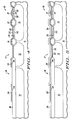
- FIG. 1 schematically illustrates an enlarged cross-sectional portion of an integrated pressure sensor 10 that includes a pressure sensor and CMOS circuits built on a monolithic semiconductor substrate 11.
- Substrate 11 is formed of a first conductivity type and has a sensor portion or sensor area generally designated as 16 and a CMOS portion or CMOS area generally designated as 17. In the preferred embodiment, substrate 11 is P-type.
- Substrate 11 includes a first well area 12 or sensor well 12 and a second well area 13 both of the second conductivity type on a surface of substrate 11.
- Well areas 12 and 13 are formed by techniques that are well known to those skilled in the semiconductor art.
- well areas 12 and 13 are formed by oxidizing the surface of substrate 11 and utilizing a silicon nitride mask to expose portions of the surface of substrate 11 followed by implanting N-type dopants into the exposed portions of substrate 11 followed by an oxidation to form oxide layers overlying well areas 12 and 13. Thereafter in this preferred embodiment, the nitride mask is removed and dopants of the first conductivity type are implanted into the surface of substrate 11 in the area where third well area 14 is formed. Subsequently, the dopants of well areas 12, 13, and 14 are driven into substrate 11 to form well areas 12, 13, and 14. In this preferred embodiment, third well area 14 has a P-type doping that is five to one hundred times higher than that of substrate 11.
- well area 13 is often referred to as an N-type well 13 and well area 14 is referred to as a P-type well 14.
- well area 12 will function as an RF/EMI shield that minimizes variations in the capacitance of sensor 10 due to RF/EMI interference.
- FIG. 2 schematically illustrates a subsequent stage of manufacturing sensor 10.
- a sensor isolation 18 is formed in the surface of substrate 11 overlying well area 12 and extending into well area 13. Isolation 18 will subsequently serve to isolate the pressure sensor from other CMOS circuitry formed in substrate 11.
- Isolation 18 can be a variety of isolation areas such as a field oxide area, an oxide or nitride layer deposited on substrate 11, a poly layer that is oxidized, or other isolations that are well known to those skilled in the art.
- Isolation 18 is formed in sensor area 16 of sensor 10. In the preferred embodiment, isolation 18 is a first field oxide.
- a well isolation field oxide 19 is formed in the surface of substrate 11 between well area 13 and well area 14 and a well isolation field oxide 21 is formed on the surface of substrate 11 and within well area 14.
- Field oxide 19 and accompanying field dopant 20 is used to isolate the CMOS transistors utilized in the CMOS devices formed in sensor 10 while field oxide 21 and accompanying field dopant 20 is utilized to isolate devices formed within well area 14.
- Field oxides 19, and 21 and field dopant 20 are formed by techniques that are well known to those skilled in the semiconductor art.
- isolation 18 is between 0.3 to 1.0 microns thick and preferably is about 0.75 microns.
- isolation 18 or first field oxide 18, second field oxide 19 or well isolation field oxide 19, and third field oxide 21 or cell isolation field oxide 21 are formed simultaneously.
- a P-type transistor subsequently formed in well area 14 is isolated from a subsequent EEPROM cell that is also formed in well 14.
- a thin blanket tunnel oxide layer 22 is applied covering isolation 18, field oxides 19 and 21, and the surface of well areas 13 and 14.
- layer 22 will subsequently be utilized to form an EEPROM cell within well area 14.
- Such tunnel oxide layers are formed by techniques that are well known to those skilled in the semiconductor art including oxidation in a nitrous oxide (N 2 O) environment in order to accurately control the thickness of layer 22.
- layer 22 is generally very thin. Layer 22 has a thickness in the range of three to fifteen nanometers and preferably is about 0.5 to 1.0 nanometers. Thereafter, a floating gate blanket polysilicon layer 23 is applied covering layer 22.
- isolation 18 can be formed by forming a trench in substrate 11 so that the trench has a surface area sufficient for forming the diaphragm of sensor 10, typically about the area of isolation of the preferred embodiment. Thereafter, a thermal oxidation is performed to for the insulation layer on the surface of the trench and extending up onto the substrate surface. Often, a chemical mechanical polishing or other technique is used to planarize the surface of substrate 11 following such oxidations.
- tunneling oxide, floating gate, gate oxide, or gate poly (discussed subsequently) formation steps to form the fixed electrode of sensor 10 facilitates the integration into a CMOS process flow and reduces the formation costs along with improving the device characteristics.
- FIG. 3 illustrates sensor 10 after subsequent processing.
- Layers 23 and 22 (shown in FIG. 2 ) are patterned and etched to form a first doped polysilicon area 28 or fixed electrode 28 of sensor 10 on an electrode tunneling oxide area or first tunneling oxide area 24 that is on the surface of isolation 18.
- a contact polysilicon area 29 or sensor contact 29 and a contact tunneling oxide area 26 are concurrently formed on the surface of isolation 18 with electrode 28.
- electrode 28 and sensor contact 29 are electrically continuous on the surface of isolation 18.
- layer 22 over isolation 18 may be too thin to be detected or may not even be non-existent.
- a floating gate area or second doped polysilicon area 31 is formed on a floating gate tunneling oxide layer 27 or second tunneling oxide area 27 concurrently with electrode 28 and sensor contact 29.
- the patterning and etching forms second tunneling oxide area 27 on the surface of substrate 11 adjacent field oxide 21.
- the patterning and etching steps utilized are well known to those skilled in the semiconductor art. It should also be noted that the conductive material of electrode 28 and contact 29 may be formed by separate steps such as forming and patterning a separate doped poly layer.
- a mask is subsequently applied to facilitate implanting dopants into well 14 adjacent second doped poly area 31 to form doped regions 52. Regions 52 will be utilized as portions of an EEPROM cell that will be formed as a part of sensor 10. Typically, a gate oxide is formed covering sensor 10 and removed from sensor area 16 by techniques that are well known to those skilled in the art. Another mask is applied to facilitate the implanting of dopants as doped region 53 to adjust the threshold of the transistor to be formed in well 14 between field oxides 19 and 21.
- FIG. 4 illustrates sensor 10 at a subsequent stage after the formation of a protective layer 35 covering CMOS area 17 and extending into sensor area 16 up to sensor contact 29.
- Protective layer 35 includes a second polysilicon layer 32 and an etch stop layer 33 covering layer 32.
- Layers 32 and 33 are formed by a blanket deposition of polysilicon followed by a blanket deposition of the etch stop material followed by patterning and etching of both to remove the portions of layers 32 and 33 over portions of sensor area 16 thereby leaving protective layer 35, including layers 32 and 33, on the surface of well area 14 and area 31, extending over field oxide 21 and across well area 14 and over field oxide 19, across well area 13, and onto isolation 18 adjacent an edge of sensor contact 29.
- Layer 32 will subsequently be used to form gate of CMOS transistors.
- etch stop layer 33 is Tetraethylorthosilicate (TEOS).
- FIG. 5 illustrates the results of subsequent processing preformed on sensor 10.
- a sensor nitride layer 34 is formed on isolation 18 and overlapping onto the edges of electrode 28, and extending into CMOS area 17 overlying well areas 13 and 14 and overlying field oxides 19 and 21.
- nitride layer 34 is a low stress silicon-rich silicon nitride layer 34 formed by blanket deposition and subsequent patterning and etching that exposes electrode 28.
- layer 34 can be a silicon nitride stochiometric layer.
- FIG. 6 illustrates sensor 10 after the subsequent formation of a sacrificial layer having a sensor area or first sacrificial layer portion 36 and a CMOS area or second sacrificial layer portion 37.
- First sacrificial layer portion 36 is formed on electrode 28 and extending out onto layer 34 and second sacrificial layer portion 37 is formed on the portion of layer 34 that overlays sensor contact 29 well areas 13 and 14, and field oxides 19 and 21.
- Sacrificial layer portions 36 and 37 are formed by methods that are well known in the semiconductor art, for example, by blanket deposition of PSG and subsequent patterning and etching.
- sacrificial layer portions 36 and 37 are phosphosilicate glass (PSG) followed by subsequent annealing prior to masking and etching.
- the thickness of first sacrificial layer portion 36 is used to determine the capacitor gap of the completed pressure sensor.
- Second sacrifical layer portion 37 will be utilized to facilitate protecting CMOS area 17 during subsequent formation of the sensor diaphragm.
- Multiple sacrificial layers may be used to form portions 36 and 37.
- portions 36 and 37 have a thickness of 0.2 to 1.0 microns.
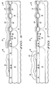
- diaphragm 38 is formed by first applying a blanket deposition of polysilicon onto the surface of sensor 10 followed by implanting dopants to form a doped polysilicon layer. A mask is then applied to protect diaphragm 38 that is to remain on sensor 10 while removing other portions of the polysilicon layer that is on second sacrificial layer portion 37 and on portions of layer 34.
- the mask has an opening overlying diaphragm 38 so that during the removal of the exposed polysilicon layer an etch release opening 54 is formed through diaphragm 38 exposing the underlying surface of first sacrificial layer portion 36.
- the etch utilized to remove the exposed polysilicon does not affect sacrificial layer portions 36 or 37 (shown in FIG. 6 ).
- a release etch is performed that removes first sacrificial layer portion 36 that is underlying diaphragm 38 and also removes second sacrificial layer portion 37 from the remaining surface of sensor 10.
- the material used in the release etch does not affect the underlying layer 34 which functions as an etch stop during this operation thereby protecting the remaining surface of sensor 10 including the surface of CMOS area 17.
- diaphragm 38 reduces stresses applied to diaphragm 38 thereby facilitating the formation of a diaphragm having a large surface area or an undercut distance at the release etch of greater than one hundred microns.
- a layer 34 thickness of 0.2 to 1.0 microns facilitates such an undercut distance.
- diaphragm 38 is formed with a compressive stress, with a thickness of one to three microns, and may be formed from multiple layers.
- FIG. 8 illustrates a subsequent manufacturing stage of sensor 10 wherein a sealing layer 39 is applied to seal diaphragm 38.
- the material may be any of those materials typically used for sealing sensor diaphragms.
- layer 39 is formed by applying a blanket deposition of TEOS using a non-conformal or line of sight deposition so that there is no lateral encroachment of the deposited TEOS. After the blanket deposition, unwanted portions of the sealing material are removed by applying a mask to protect layer 39, as indicated by a dashed line 41, while removing the sealing material from CMOS area 17 and from sensor contact 29. For example, a buffered oxide etch may be utilized to remove the unwanted portions of the sealing material.
- layer 39 has a thickness of about one to four microns. Also, other materials such as PSG, plasma enhanced nitride, and oxynitride can be used for layer 39.
- the mask is removed and the portion of layer 34 is removed from CMOS area 17 and from sensor contact 29. This leaves diaphragm 38 and sealing layer 39 residing in contact with layer 34.
- a blanket etch is utilized to remove etch stop layer 33.
- a buffered oxide etch is utilized to remove the TEOS used for etch stop layer 33.
- FIG. 9 illustrates sensor 10 after several subsequent processing operations are performed.
- a memory cell or EEPROM cell identified by a dashed box 46 is formed in well area 14, and N and P CMOS transistors are formed in well areas 13 and 14 respectively.
- the exposed protective poly layer 32 is patterned and etched to form transistor gates 56 and an active gate 57 of the EEPROM cell.
- Gates 56 will become the gates of CMOS transistors of transistors 43 and 44 (shown generally by dashed boxes) that will be formed in well areas 13 and 14.
- the formation of transistor gates 56 and active gate 57 are well known to those skilled in the art.
- sensor 10 is masked and source and drain implant areas 58 are formed adjacent transistor gates 56 in well areas 13 and 14.
- implant areas 58 may be a combination of implants to form graded source and drain areas.
- nitride spacers are formed adjacent transistor gates 56 to protect gates 56 during subsequent silicidization of gate 56. Such spacers and silicidization operations and methods are well known to those skilled in the semiconductor art.
- an activation anneal is performed in order to activate the dopants in implant areas 58.
- the activation anneal is a rapid thermal process performed at a temperature between 900 and 1100 degrees Celsius for a time of twenty to forty seconds.
- This activation also activates the dopant in diaphragm 38 and relieves stresses that are formed in diaphragm 38. Performing the activation anneal for the source drain implants and for the doped polysilicon of the diaphragm at the same time prevents the activation anneal of the diaphragm polysilicon from affecting the characteristics of the CMOS transistors.
- a pressure transducer 42 shown by a dashed box, is formed on sensor 10.
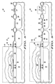
- FIG. 10 illustrates sensor 10 after forming multiple layers of metal interconnects and a passivation layer 49 protecting sensor 10.
- a first interlayer dielectric 47 and associated metal interconnects and a second interlayer dielectric 48 and a device electrode 51 are formed by techniques that are well known to those skilled in the semiconductor art. Methods for forming passivation layer 49 overlying sensor 10 are well known to those skilled in the semiconductor art. Subsequently, portions of passivation layer 49 are removed to expose device electrode 51 and diaphragm 38.
- passivation layer 49 is a layer of oxynitride however a variety of well known passivation materials may be used including silicon dioxide.
- a mask is applied to passivation layer 49 and patterned to have openings corresponding to where a sensor opening 61 and a contact opening 62 are to be formed.
- a wet buffered oxide etch (BOE) is utilized to remove the exposed portions of passivation layer 49. The etch is stopped prior to exposing the metal of device electrode 51 in order to prevent the BOE from staining the metal of contact 51.
- a dry etch is utilized to expose contact 51 and to remove the dielectrics overlying diaphragm 38 and sealing layer 39. This dry etch must stop upon exposing diaphragm 38 in order to prevent etching or damaging diaphragm 38.
- transducer 42 As is well known in the art, another pressure transducer similar to transducer 42 is formed on a portion of sensor 10 distal to transducer 42 in order to form a differential capacitor sensor.
- opening 61 may be formed in dielectric 47 and the underlying portion of sealing layer 39 removed at the same time that openings are formed for the metal contacts that go through dielectric 47. In this embodiment, it is important to remove all metal that is formed overlying diaphragm 38 on dielectric 47 in order to prevent the metal from affecting the capacitance of sensor 10. Thereafter, opening 61 would be formed in dielectric 48 simultaneously with forming the opening for the metal of contact 51. All metal would also have to be removed on the surface of dielectric 48 that overlies diaphragm 38. Thereafter, opening 61 would be formed in passivation layer 49 simultaneously with the formation of opening 62.
- a mask is applied exposing the area of passivation layer 49 where openings 61 and 62 are to be formed.
- a dry etch is utilized to form opening 61 and 62 through layer 49 and to continue down through dielectrics 48 and 47 to expose sealing layer 39.
- Another mask is applied to protect opening 62 and expose opening 61 during a wet etch used to remove the material of sealing layer 39 thereby exposing diaphragm 38.
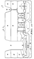
- FIG. 11 illustrates an alternate embodiment of sensor 10 that provides sensor 10 with a more planar surface by recessing the diaphragm and sealing layer to a level that is more planar with the surface provided by transistors 43 and 44.
- a recess or moat is formed in well area 12 prior to the formation of field oxide 18.
- the moat within well area 12 may be formed by various well known techniques, for example anisotropic etching, that create V-shaped or sloping sides to make subsequent processing steps easier to perform.
- a mask is applied exposing the area of passivation layer 49 where opening 62 is formed.
- a dry etch is used to form opening 61.
- Another mask is then applied to expose the area of passivation where opening 61 is formed.
- a wet etch is then utilized to remove the materials in layer 49, layer 48, layer 47, and layer 39 exposing diaphragm 38.
- Forming the diaphragm and fixed electrode on an isolation layer such as field oxide isolates the diaphragm and fixed electrode from the CMOS and other active elements of sensor 10.
- Forming the fixed electrode on a thin oxide layer simultaneously with the floating gate electrode of an EEPROM cell minimizes the processing steps required to form the fixed electrode.
- Forming the doped polysilicon diaphragm prior to implanting source and drain areas of the CMOS transistors and annealing the polysilicon diaphragm along with the source and drain implants insures that the annealing of the polysilicon diaphragm does not detrimentally affect the characteristics of the CMOS transistors.
Landscapes
- Physics & Mathematics (AREA)
- General Physics & Mathematics (AREA)
- Measuring Fluid Pressure (AREA)
- Pressure Sensors (AREA)
- Metal-Oxide And Bipolar Metal-Oxide Semiconductor Integrated Circuits (AREA)
Claims (3)
- Verfahren zum Bilden eines integrierten CMOS (komplementärer Metall-Oxid-Halbleiter)-Drucksensors (10), das umfasst:Bilden eines Halbleitersubstrates (11) eines ersten Leitfähigkeitstyps mit einem Sensorbereich (16) und einem CMOS-Bereich (17);Bilden eines Sensordiaphragmas (38), welches über einer festen Elektrode (28) des Sensors liegt, welcher über eine Sensorisolierung (18) liegt;danach Bilden von Source- und Drainbereichen (58) von CMOS-Transistoren in einer Fläche des Halbleitersubstrates (11) und innerhalb des CMOS-Bereiches des Halbleitersubstrates vor dem Tempern des Sensordiaphragmas (38); und
Tempern des Sensordiaphragmas (38) und der Source- und Drainbereiche (58), wobei das Verfahren gekennzeichnet ist durch:Bilden der festen Elektrode auf einem ersten Abschnitt (24) einer Tunneloxidschicht (22), wobei ein schwebendes Gatter (31) einer Speicherzelle (46) in dem CMOS-Bereich auf einem zweiten Abschnitt (27) der Tunneloxidschicht (22) gebildet wird. - Verfahren gemäß Anspruch 1, wobei das Bilden des Sensordiaphragmas (38) ein Bilden des Sensordiaphragmas aus dotiertem Polysilizium beinhaltet, welches über der festen Elektrode (28) und der Sensorisolierung (18) liegt.
- Verfahren gemäß Anspruch 1, wobei das schwebende Gatter (31) der Vorrichtung in dem CMOS-Bereich ein schwebendes Gatter einer EEPROM-Zelle ist.
Applications Claiming Priority (3)
| Application Number | Priority Date | Filing Date | Title |
|---|---|---|---|
| US09/734,473 US6472243B2 (en) | 2000-12-11 | 2000-12-11 | Method of forming an integrated CMOS capacitive pressure sensor |
| US734473 | 2000-12-11 | ||
| PCT/US2001/044013 WO2002048668A2 (en) | 2000-12-11 | 2001-11-19 | Integrated cmos capacitive pressure sensor |
Publications (2)
| Publication Number | Publication Date |
|---|---|
| EP1344035A2 EP1344035A2 (de) | 2003-09-17 |
| EP1344035B1 true EP1344035B1 (de) | 2010-06-16 |
Family
ID=24951833
Family Applications (1)
| Application Number | Title | Priority Date | Filing Date |
|---|---|---|---|
| EP01989753A Expired - Lifetime EP1344035B1 (de) | 2000-12-11 | 2001-11-19 | Integrierter kapazitiver cmos-drucksensor |
Country Status (6)
| Country | Link |
|---|---|
| US (1) | US6472243B2 (de) |
| EP (1) | EP1344035B1 (de) |
| JP (1) | JP4267322B2 (de) |
| AU (1) | AU2002228637A1 (de) |
| DE (1) | DE60142406D1 (de) |
| WO (1) | WO2002048668A2 (de) |
Families Citing this family (34)
| Publication number | Priority date | Publication date | Assignee | Title |
|---|---|---|---|---|
| US6664909B1 (en) * | 2001-08-13 | 2003-12-16 | Impinj, Inc. | Method and apparatus for trimming high-resolution digital-to-analog converter |
| US6828172B2 (en) * | 2002-02-04 | 2004-12-07 | Delphi Technologies, Inc. | Process for a monolithically-integrated micromachined sensor and circuit |
| US20040206999A1 (en) * | 2002-05-09 | 2004-10-21 | Impinj, Inc., A Delaware Corporation | Metal dielectric semiconductor floating gate variable capacitor |
| DE10245627B3 (de) * | 2002-09-30 | 2004-05-06 | Infineon Technologies Ag | Fingerabdrucksensor |
| US7115438B2 (en) * | 2004-04-29 | 2006-10-03 | United Microelectronics Corp. | Method for manufacturing a complementary metal-oxide semiconductor sensor |
| JP5280609B2 (ja) | 2004-10-01 | 2013-09-04 | 株式会社日立製作所 | 半導体装置およびその製造方法 |
| US7121146B1 (en) * | 2004-10-29 | 2006-10-17 | National Semiconductor Corporation | MEMS pressure sensing device |
| US7328609B1 (en) | 2004-10-29 | 2008-02-12 | National Semiconductor Corporation | Wireless pressure sensing Schrader valve |
| US7109055B2 (en) * | 2005-01-20 | 2006-09-19 | Freescale Semiconductor, Inc. | Methods and apparatus having wafer level chip scale package for sensing elements |
| JP4501715B2 (ja) * | 2005-02-16 | 2010-07-14 | セイコーエプソン株式会社 | Mems素子およびmems素子の製造方法 |
| US7284418B2 (en) * | 2005-06-03 | 2007-10-23 | Temic Automotive Of North America, Inc. | Tire pressure sensor assembly |
| US7281421B2 (en) * | 2005-06-03 | 2007-10-16 | Temic Automotive Of North America, Inc. | Package for a tire pressure sensor assembly |
| JP4988217B2 (ja) * | 2006-02-03 | 2012-08-01 | 株式会社日立製作所 | Mems構造体の製造方法 |
| US7632698B2 (en) | 2006-05-16 | 2009-12-15 | Freescale Semiconductor, Inc. | Integrated circuit encapsulation and method therefor |
| US7528468B2 (en) * | 2006-09-25 | 2009-05-05 | Freescale Semiconductor, Inc. | Capacitor assembly with shielded connections and method for forming the same |
| JP5127210B2 (ja) * | 2006-11-30 | 2013-01-23 | 株式会社日立製作所 | Memsセンサが混載された半導体装置 |
| JP4337870B2 (ja) | 2006-12-15 | 2009-09-30 | セイコーエプソン株式会社 | Memsレゾネータ及びmemsレゾネータの製造方法 |
| JP4947065B2 (ja) * | 2009-01-09 | 2012-06-06 | セイコーエプソン株式会社 | Memsレゾネータの製造方法 |
| GB2467776A (en) * | 2009-02-13 | 2010-08-18 | Wolfson Microelectronics Plc | Integrated MEMS transducer and circuitry |
| JP2011158317A (ja) * | 2010-01-29 | 2011-08-18 | Panasonic Electric Works Co Ltd | 圧力センサ |
| CN102856177B (zh) * | 2011-06-27 | 2015-01-28 | 中芯国际集成电路制造(北京)有限公司 | 半导体器件和用于制造半导体器件的方法 |
| KR101781553B1 (ko) * | 2011-08-22 | 2017-09-26 | 삼성전자주식회사 | 용량성 트랜스듀서와 그 제조 및 동작방법 |
| US10094988B2 (en) * | 2012-08-31 | 2018-10-09 | Micron Technology, Inc. | Method of forming photonics structures |
| DE102012023429B8 (de) * | 2012-11-29 | 2013-10-24 | Elmos Semiconductor Ag | CMOS kompatibler Drucksensor auf Tunneleffekt-Basis mit Verfahren |
| JP5832417B2 (ja) * | 2012-12-07 | 2015-12-16 | 三菱電機株式会社 | 半導体圧力センサおよびその製造方法 |
| EP3604207A1 (de) | 2013-03-05 | 2020-02-05 | Ams Ag | Halbleiterbauelement mit kapazitivem sensor und integrierter schaltung |
| JP5933480B2 (ja) * | 2013-04-26 | 2016-06-08 | 三菱電機株式会社 | 半導体圧力センサおよびその製造方法 |
| JP6119615B2 (ja) * | 2014-01-08 | 2017-04-26 | 三菱電機株式会社 | 半導体装置の製造方法 |
| JP6433349B2 (ja) * | 2015-03-19 | 2018-12-05 | 三菱電機株式会社 | 半導体圧力センサおよびその製造方法 |
| US20170115322A1 (en) * | 2015-10-22 | 2017-04-27 | Freescale Semiconductor, Inc. | Mems sensor device having integrated multiple stimulus sensing |
| JP6532429B2 (ja) | 2016-06-01 | 2019-06-19 | 三菱電機株式会社 | 半導体圧力センサ |
| EP3261366B1 (de) | 2016-06-21 | 2021-09-22 | Sciosense B.V. | Mikrofon- und drucksensorverpackung sowie verfahren zur herstellung des mikrofons und der drucksensorverpackung |
| EP3260821B1 (de) | 2016-06-21 | 2019-09-11 | ams International AG | Sensorpaket und verfahren zur herstellung des sensorpakets |
| CN108183163A (zh) * | 2018-01-08 | 2018-06-19 | 杭州士兰微电子股份有限公司 | 一种超声波传感器的制造方法 |
Family Cites Families (3)
| Publication number | Priority date | Publication date | Assignee | Title |
|---|---|---|---|---|
| DE4042336A1 (de) | 1990-02-12 | 1991-08-14 | Fraunhofer Ges Forschung | Drucksensoranordnung mit einem drucksensor und einem referenzelement |
| US5431057A (en) | 1990-02-12 | 1995-07-11 | Fraunhofer-Gesellschaft Zur Forderung Der Angewandten Forschung E.V. | Integratable capacitative pressure sensor |
| US6012336A (en) * | 1995-09-06 | 2000-01-11 | Sandia Corporation | Capacitance pressure sensor |
-
2000
- 2000-12-11 US US09/734,473 patent/US6472243B2/en not_active Expired - Lifetime
-
2001
- 2001-11-19 WO PCT/US2001/044013 patent/WO2002048668A2/en not_active Ceased
- 2001-11-19 EP EP01989753A patent/EP1344035B1/de not_active Expired - Lifetime
- 2001-11-19 DE DE60142406T patent/DE60142406D1/de not_active Expired - Lifetime
- 2001-11-19 JP JP2002549926A patent/JP4267322B2/ja not_active Expired - Fee Related
- 2001-11-19 AU AU2002228637A patent/AU2002228637A1/en not_active Abandoned
Also Published As
| Publication number | Publication date |
|---|---|
| DE60142406D1 (de) | 2010-07-29 |
| US20020072144A1 (en) | 2002-06-13 |
| US6472243B2 (en) | 2002-10-29 |
| WO2002048668A3 (en) | 2002-10-10 |
| EP1344035A2 (de) | 2003-09-17 |
| JP2004526299A (ja) | 2004-08-26 |
| WO2002048668A2 (en) | 2002-06-20 |
| JP4267322B2 (ja) | 2009-05-27 |
| AU2002228637A1 (en) | 2002-06-24 |
Similar Documents
| Publication | Publication Date | Title |
|---|---|---|
| US6472243B2 (en) | Method of forming an integrated CMOS capacitive pressure sensor | |
| US6074914A (en) | Integration method for sidewall split gate flash transistor | |
| JP5933480B2 (ja) | 半導体圧力センサおよびその製造方法 | |
| CN100527386C (zh) | 半导体器件的制造方法 | |
| KR940007654B1 (ko) | 불휘발성 반도체 메모리장치의 제조방법 | |
| JP2014115153A (ja) | 半導体圧力センサおよびその製造方法 | |
| KR20020070356A (ko) | Locos/sti 분리 및 플래시메모리 회로의 질화터널산화물을 위한 질화장벽 | |
| KR20020070075A (ko) | 비휘발성 반도체 기억 장치 및 그 제조 방법 | |
| JPH0851144A (ja) | 半導体集積回路の一部の構成体及びその製造方法 | |
| WO2003036702A2 (en) | Integrated circuit having interconnect to a substrate and method therefor | |
| KR100515181B1 (ko) | 반도체 장치의 제조 방법 | |
| KR20020066934A (ko) | 비휘발성 반도체 기억 장치 및 그 제조 방법 | |
| KR19980086998A (ko) | Soi 구조를 가지는 반도체장치 및 그 제조방법 | |
| JP2007096310A (ja) | 半導体装置の製造方法 | |
| JPH1145874A (ja) | 半導体装置の製造方法 | |
| US20030003700A1 (en) | Methods providing oxide layers having reduced thicknesses at central portions thereof and related devices | |
| KR100823395B1 (ko) | 반도체 장치 및 그 제조 방법 | |
| EP2423952B1 (de) | Strukturierung eines Gatestapels eines nichtflüchtigen Speichers mit simultaner Ätzung im nichtflüchtigen Speicherbereich | |
| JP2882395B2 (ja) | 半導体集積回路装置及びその製造方法 | |
| JP2003017596A (ja) | 半導体記憶装置の製造方法 | |
| Gianchandani et al. | A fabrication process for integrating polysilicon microstructures with post-processed CMOS circuits | |
| US6346429B1 (en) | Method for fabricating integrated sensors | |
| EP1231631A2 (de) | MFMOS/MFMS-Festwertspeichertransistoren und deren Herstellungsverfahren | |
| JP3360970B2 (ja) | 半導体装置の製造方法 | |
| JP4345889B2 (ja) | Flotox型eepromの製造方法 |
Legal Events
| Date | Code | Title | Description |
|---|---|---|---|
| PUAI | Public reference made under article 153(3) epc to a published international application that has entered the european phase |
Free format text: ORIGINAL CODE: 0009012 |
|
| 17P | Request for examination filed |
Effective date: 20030711 |
|
| AK | Designated contracting states |
Kind code of ref document: A2 Designated state(s): AT BE CH CY DE DK ES FI FR GB GR IE IT LI LU MC NL PT SE TR |
|
| AX | Request for extension of the european patent |
Extension state: AL LT LV MK RO SI |
|
| RBV | Designated contracting states (corrected) |
Designated state(s): DE FR GB NL |
|
| RAP1 | Party data changed (applicant data changed or rights of an application transferred) |
Owner name: FREESCALE SEMICONDUCTOR, INC. |
|
| 17Q | First examination report despatched |
Effective date: 20081211 |
|
| GRAP | Despatch of communication of intention to grant a patent |
Free format text: ORIGINAL CODE: EPIDOSNIGR1 |
|
| GRAS | Grant fee paid |
Free format text: ORIGINAL CODE: EPIDOSNIGR3 |
|
| GRAA | (expected) grant |
Free format text: ORIGINAL CODE: 0009210 |
|
| AK | Designated contracting states |
Kind code of ref document: B1 Designated state(s): DE FR GB NL |
|
| REF | Corresponds to: |
Ref document number: 60142406 Country of ref document: DE Date of ref document: 20100729 Kind code of ref document: P |
|
| REG | Reference to a national code |
Ref country code: NL Ref legal event code: VDEP Effective date: 20100616 |
|
| PG25 | Lapsed in a contracting state [announced via postgrant information from national office to epo] |
Ref country code: NL Free format text: LAPSE BECAUSE OF FAILURE TO SUBMIT A TRANSLATION OF THE DESCRIPTION OR TO PAY THE FEE WITHIN THE PRESCRIBED TIME-LIMIT Effective date: 20100616 |
|
| PLBE | No opposition filed within time limit |
Free format text: ORIGINAL CODE: 0009261 |
|
| STAA | Information on the status of an ep patent application or granted ep patent |
Free format text: STATUS: NO OPPOSITION FILED WITHIN TIME LIMIT |
|
| 26N | No opposition filed |
Effective date: 20110317 |
|
| REG | Reference to a national code |
Ref country code: DE Ref legal event code: R097 Ref document number: 60142406 Country of ref document: DE Effective date: 20110316 |
|
| REG | Reference to a national code |
Ref country code: FR Ref legal event code: PLFP Year of fee payment: 15 |
|
| PGFP | Annual fee paid to national office [announced via postgrant information from national office to epo] |
Ref country code: GB Payment date: 20151127 Year of fee payment: 15 |
|
| REG | Reference to a national code |
Ref country code: DE Ref legal event code: R081 Ref document number: 60142406 Country of ref document: DE Owner name: NORTH START INNOVATIONS INC., COSTA MESA, US Free format text: FORMER OWNER: FREESCALE SEMICONDUCTOR, INC., AUSTIN, TEX., US Ref country code: DE Ref legal event code: R081 Ref document number: 60142406 Country of ref document: DE Owner name: NORTH STAR INNOVATIONS INC., COSTA MESA, US Free format text: FORMER OWNER: FREESCALE SEMICONDUCTOR, INC., AUSTIN, TEX., US |
|
| REG | Reference to a national code |
Ref country code: DE Ref legal event code: R081 Ref document number: 60142406 Country of ref document: DE Owner name: NORTH STAR INNOVATIONS INC., COSTA MESA, US Free format text: FORMER OWNER: NORTH START INNOVATIONS INC., COSTA MESA, CALIF., US Ref country code: DE Ref legal event code: R082 Ref document number: 60142406 Country of ref document: DE Representative=s name: SCHUMACHER & WILLSAU PATENTANWALTSGESELLSCHAFT, DE |
|
| REG | Reference to a national code |
Ref country code: GB Ref legal event code: 732E Free format text: REGISTERED BETWEEN 20160303 AND 20160309 |
|
| REG | Reference to a national code |
Ref country code: FR Ref legal event code: TP Owner name: NORTH STAR INNOVATIONS INC., US Effective date: 20160401 |
|
| REG | Reference to a national code |
Ref country code: FR Ref legal event code: PLFP Year of fee payment: 16 |
|
| PGFP | Annual fee paid to national office [announced via postgrant information from national office to epo] |
Ref country code: FR Payment date: 20161123 Year of fee payment: 16 Ref country code: DE Payment date: 20161123 Year of fee payment: 16 |
|
| GBPC | Gb: european patent ceased through non-payment of renewal fee |
Effective date: 20161119 |
|
| PG25 | Lapsed in a contracting state [announced via postgrant information from national office to epo] |
Ref country code: GB Free format text: LAPSE BECAUSE OF NON-PAYMENT OF DUE FEES Effective date: 20161119 |
|
| REG | Reference to a national code |
Ref country code: DE Ref legal event code: R119 Ref document number: 60142406 Country of ref document: DE |
|
| REG | Reference to a national code |
Ref country code: FR Ref legal event code: ST Effective date: 20180731 |
|
| PG25 | Lapsed in a contracting state [announced via postgrant information from national office to epo] |
Ref country code: DE Free format text: LAPSE BECAUSE OF NON-PAYMENT OF DUE FEES Effective date: 20180602 Ref country code: FR Free format text: LAPSE BECAUSE OF NON-PAYMENT OF DUE FEES Effective date: 20171130 |