EP1332517B1 - Procede de revelation de defauts cristallins et/ou de champs de contraintes a l'interface d'adhesion moleculaire de deux materiaux solides - Google Patents
Procede de revelation de defauts cristallins et/ou de champs de contraintes a l'interface d'adhesion moleculaire de deux materiaux solides Download PDFInfo
- Publication number
- EP1332517B1 EP1332517B1 EP01974440A EP01974440A EP1332517B1 EP 1332517 B1 EP1332517 B1 EP 1332517B1 EP 01974440 A EP01974440 A EP 01974440A EP 01974440 A EP01974440 A EP 01974440A EP 1332517 B1 EP1332517 B1 EP 1332517B1
- Authority
- EP
- European Patent Office
- Prior art keywords
- crystalline
- thin film
- defects
- treatment
- stress fields
- Prior art date
- Legal status (The legal status is an assumption and is not a legal conclusion. Google has not performed a legal analysis and makes no representation as to the accuracy of the status listed.)
- Expired - Lifetime
Links
Images

Classifications
-
- H—ELECTRICITY
- H10—SEMICONDUCTOR DEVICES; ELECTRIC SOLID-STATE DEVICES NOT OTHERWISE PROVIDED FOR
- H10P—GENERIC PROCESSES OR APPARATUS FOR THE MANUFACTURE OR TREATMENT OF DEVICES COVERED BY CLASS H10
- H10P50/00—Etching of wafers, substrates or parts of devices
-
- H—ELECTRICITY
- H10—SEMICONDUCTOR DEVICES; ELECTRIC SOLID-STATE DEVICES NOT OTHERWISE PROVIDED FOR
- H10P—GENERIC PROCESSES OR APPARATUS FOR THE MANUFACTURE OR TREATMENT OF DEVICES COVERED BY CLASS H10
- H10P10/00—Bonding of wafers, substrates or parts of devices
- H10P10/12—Bonding of semiconductor wafers or semiconductor substrates to semiconductor wafers or semiconductor substrates
- H10P10/128—Bonding of semiconductor wafers or semiconductor substrates to semiconductor wafers or semiconductor substrates by direct semiconductor to semiconductor bonding
Definitions
- the invention relates to a method for revealing defects or stresses in a structure, in particular for producing nanostructures or microstructures, this method using molecular bonding of two crystalline elements.
- the document WO 99/05711 discloses a process using a molecular bonding of two platelets of crystalline material to obtain a nanometric or micrometric network of stress fields and / or crystalline defects.
- a chemical or mechanical thinning method one of the platelets is thinned sufficiently to reveal the network of crystal defects or stress fields. If a material is then deposited on the film constituted by the thinned plate, this material is organized in a network which depends directly on the network of crystalline defects and / or stress fields induced at the bonding interface and revealed by the film. slim.
- dislocations which are the privileged place of precipitation, are randomly distributed in a volume and are not unique or perfectly controlled.
- the object of the invention is to make a manometric or micrometric network of stress fields and / or crystalline defects usable for using this network in a different way than the current methods.
- the thermal budget may be provided during an operation for modifying at least one of the properties of the material presented by the free face of the thin film. These properties may include its nature, surface topology, and internal stress fields. It can also be made during an operation for depositing on the free face of the thin film.
- the introduction of chemical species into the thin film can be achieved by a method chosen from ion implantation and diffusion.
- Introduced chemical species may be species that precipitate or focus on crystalline defects and / or under the influence of stress fields.
- Thin film processing may be performed locally to reveal one or more areas of the lattice of crystal defects and / or stress fields.
- the processing step may be applied to one or more of said thin films.
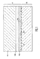
- the figure 1 is a sectional cross-sectional view showing an SOI substrate 1 bonded to a silicon wafer 2.
- the SOI substrate 1 is for example a disk 4 inches (10.16 cm) in diameter, consisting of the superposition of a wafer 11 of silicon, a layer 12 of SiO 2 400 nm thick and a silicon layer 13 of 200 nm thick.
- the layer 13 has a bonding face 14.
- the silicon of the wafers 11 and the silicon of the layer 13 are each P-type doped with 10 15 -10 16 atoms / cm 3 .
- the layer 13 has a surface oriented in the ⁇ 100> direction.
- the wafer 2, 4 inches (10.16 cm) in diameter is also of P-type silicon doped with 10 15 -10 16 atoms / cm 3 and has a surface oriented in the ⁇ 100> direction.
- the wafer 2 has a bonding face 21.
- the figure 1 shows the structure obtained after adhesion by molecular adhesion of the face 21 of the wafer 2 on the face 14 of the SOI substrate 1.
- the faces 21 and 14 have been treated by a method of the known art so as to obtain the molecular adhesion.
- the substrate 1 and the wafer 2 are bonded so that the faces 14 and 21 have staggered crystal lattices as shown in the document WO 99/05711 .
- the structure may be subjected to a heat treatment which reinforces the seal between the faces 12 and 21.
- the adhesion by molecular adhesion causes the formation of a network of crystalline defects and / or stress fields symbolically represented under the reference 3 on the figure 1 .
- the next step of the process will consist in thinning the substrate 1.
- the SOI substrate 1 is thinned from its rear face by a mechanical method of the known art.
- This mechanical thinning is, for example, stopped more than 10 ⁇ m from the bonding interface 14/21 and therefore in the silicon wafer 11.
- the rest of the silicon of the wafer 11 is removed for example by etching using TMAH (trimethylammonium hydroxide) at 80 ° C. Other types of thinning may be used.
- TMAH trimethylammonium hydroxide
- Other types of thinning may be used.
- This etching stops on the back side of the oxide layer 12.
- the oxide layer 12 is then removed by etching with a solution of hydrofluoric acid (10% HF: H 2 O).
- the next step of the process consists in treating the thin film 16 so that its free face 15 reveals the network of crystalline defects or stress fields existing in the vicinity of the bonding interface 14/21.
- the network of crystalline defects or stress fields can be revealed by the contribution of a thermal budget.
- This thermal budget can be provided during an annealing under different atmospheres (nitrogen, oxygen, argon or any other gas), or under vacuum, during epitaxy, during an oxidation or by a combination of these techniques.
- This thermal budget is intended to cause a change in the volume of stress zones and / or crystalline defects.
- This change in volume causes a modification of the topology of the free surface 15 of the film 16. It leads to the appearance on the surface of a network of constraints or a periodic topological modification of the surface depending wholly or in part on the network constraint fields and / or the network of crystalline defects present at and / or in the vicinity of the bonding interface whose volume has been modified.
- the pitch of the modified topology may be a multiple of the pitch of the network of stress fields and / or the lattice of crystalline defects.
- the figure 3 shows, under the reference 18, an example of topographic modulation of the surface of the film 16 after vacuum annealing at a temperature of 800 ° C.
- This modulation of the surface is periodic and the modulation period depends on the period of the dislocation networks present at the bonding interface 14/21, that is to say at about 10 nm below the free surface of the film 16.
- the network of crystal defects or stress fields can also be revealed by the introduction of chemical species into the thin film.
- chemical species can come from metallic or magnetic particles. It can be gases, for example hydrogen and / or helium or one or more other elements that can be introduced into the thin film 16 or in the wafer 2, for example Er, Fe, Co, Ni, Mn, Au, Cu.
- the introduction of species can be done by diffusion or ion implantation for example. It can consist in introducing several different species in one or more stages.
- the introduction of chemical species can be followed and / or preceded and / or at the same time as the contribution of a thermal budget that can be divided into several phases.
- This thermal budget can, in addition to the various effects mentioned above, facilitate the diffusion of the various species introduced to the crystalline defects. This can make it possible to reduce or increase the volume of the constraint field network locally and / or to modify the nature of the lattice defects that are networked.
- this change in volume and / or nature of the stresses and / or crystalline defects can be reflected in the surface.
- Introduced species may further precipitate on crystal defects and / or the influence of stress fields.
- the pitch of the network of buried species can be multiple of the pitch of the network of stress fields and / or the lattice of crystalline defects.
- a copper introduction it is possible to obtain a nanometric nanoscale wire network at an Si / Si interface, which can be shown on the surface.
- the network of crystalline defects or stress fields can also be revealed by at least one chemical and / or electrochemical and / or ionic and / or photochemical attack and / or mechanical attack. It may be for example a RIE etching or an ion bombardment. This treatment can be done after and / or before and / or during the supply of a thermal budget leading to the modification of the network of stresses and / or crystalline defects. There is a good modification of the volume of the stresses and / or the crystalline defects in the sense that the volume of the extension of the stress fields and / or crystalline defects is modified. The location of this attack totally or partially depends on the network of stress fields and / or the lattice of crystalline defects.
- the pitch of this localized attack may be a multiple of the constraint field network pitch and / or the crystal defect network.
- the formation of porous silicon by electrochemical etching in HF will reveal a porosity or roughness depending wholly or in part on the network of stress fields and / or the lattice of crystal defects.
- the pitch of this roughness may be a multiple of the strain field network pitch and / or the crystal defect network.
- This change in volume can then be used for the organization of material deposited on this surface.
- This deposition can be done by one of the deposition techniques chosen for example from the gaseous techniques (for example, epitaxy, CVD, molecular jet techniques, spraying), by liquid means (for example, deposition of materials in solution, liquid phase epitaxy (LPE), deposition of molten polymer.) or solid (by for example solid aggregate deposition).
- gaseous techniques for example, epitaxy, CVD, molecular jet techniques, spraying
- liquid means for example, deposition of materials in solution, liquid phase epitaxy (LPE), deposition of molten polymer.
- solid by for example solid aggregate deposition.
- This deposited material may be amorphous (for example oxide or nitride), metallic (for example Co, Fe, Ni, Mn, Au, Cu or other metals), semiconductor (for example Si, Ge, SiC, compounds II-IV or III-V such as GaN, InP, AsGa, InGaAs, etc., superconducting, organic or insulating (eg diamond, graphite or other insulators).
- amorphous for example oxide or nitride
- metallic for example Co, Fe, Ni, Mn, Au, Cu or other metals
- semiconductor for example Si, Ge, SiC, compounds II-IV or III-V such as GaN, InP, AsGa, InGaAs, etc., superconducting, organic or insulating (eg diamond, graphite or other insulators).
Landscapes
- Crystals, And After-Treatments Of Crystals (AREA)
- Recrystallisation Techniques (AREA)
- Micromachines (AREA)
- Processes Of Treating Macromolecular Substances (AREA)
- Encapsulation Of And Coatings For Semiconductor Or Solid State Devices (AREA)
- Surface Treatment Of Glass (AREA)
- Measurement Of Current Or Voltage (AREA)
- Analysing Materials By The Use Of Radiation (AREA)
Applications Claiming Priority (3)
| Application Number | Priority Date | Filing Date | Title |
|---|---|---|---|
| FR0012796A FR2815121B1 (fr) | 2000-10-06 | 2000-10-06 | Procede de revelation de defauts cristallins et/ou de champs de contraintes a l'interface d'adhesion moleculaire de deux materiaux solides |
| FR0012796 | 2000-10-06 | ||
| PCT/FR2001/003074 WO2002029876A1 (fr) | 2000-10-06 | 2001-10-05 | Procede de revelation de defauts cristallins et/ou de champs de contraintes a l'interface d'adhesion moleculaire de deux materiaux solides |
Publications (2)
| Publication Number | Publication Date |
|---|---|
| EP1332517A1 EP1332517A1 (fr) | 2003-08-06 |
| EP1332517B1 true EP1332517B1 (fr) | 2009-12-09 |
Family
ID=8855073
Family Applications (1)
| Application Number | Title | Priority Date | Filing Date |
|---|---|---|---|
| EP01974440A Expired - Lifetime EP1332517B1 (fr) | 2000-10-06 | 2001-10-05 | Procede de revelation de defauts cristallins et/ou de champs de contraintes a l'interface d'adhesion moleculaire de deux materiaux solides |
Country Status (7)
| Country | Link |
|---|---|
| US (1) | US7041227B2 (enExample) |
| EP (1) | EP1332517B1 (enExample) |
| JP (2) | JP2004511102A (enExample) |
| AT (1) | ATE451716T1 (enExample) |
| DE (1) | DE60140760D1 (enExample) |
| FR (1) | FR2815121B1 (enExample) |
| WO (1) | WO2002029876A1 (enExample) |
Families Citing this family (14)
| Publication number | Priority date | Publication date | Assignee | Title |
|---|---|---|---|---|
| JP2004281878A (ja) * | 2003-03-18 | 2004-10-07 | Seiko Epson Corp | 半導体基板の製造方法及びこれにより製造される半導体基板、電気光学装置並びに電子機器 |
| JP2005279843A (ja) * | 2004-03-29 | 2005-10-13 | Univ Of Tokyo | 細線を含む結晶材料とその製造方法、およびこれを用いたナノ細線デバイス |
| US7495266B2 (en) * | 2004-06-16 | 2009-02-24 | Massachusetts Institute Of Technology | Strained silicon-on-silicon by wafer bonding and layer transfer |
| FR2876498B1 (fr) * | 2004-10-12 | 2008-03-14 | Commissariat Energie Atomique | Procede de realisation d'heterostructures resonnantes a transport planaire |
| FR2877662B1 (fr) | 2004-11-09 | 2007-03-02 | Commissariat Energie Atomique | Reseau de particules et procede de realisation d'un tel reseau. |
| CN101326646B (zh) * | 2005-11-01 | 2011-03-16 | 麻省理工学院 | 单片集成的半导体材料和器件 |
| US20070252223A1 (en) * | 2005-12-05 | 2007-11-01 | Massachusetts Institute Of Technology | Insulated gate devices and method of making same |
| FR2895419B1 (fr) | 2005-12-27 | 2008-02-22 | Commissariat Energie Atomique | Procede de realisation simplifiee d'une structure epitaxiee |
| FR2895391B1 (fr) * | 2005-12-27 | 2008-01-25 | Commissariat Energie Atomique | Procede d'elaboration de nanostructures ordonnees |
| FR2896493B1 (fr) | 2006-01-23 | 2008-02-22 | Commissariat Energie Atomique | Procede d'elaboration d'un support pour la croissance de nanostructures allongees localisees |
| US8063397B2 (en) * | 2006-06-28 | 2011-11-22 | Massachusetts Institute Of Technology | Semiconductor light-emitting structure and graded-composition substrate providing yellow-green light emission |
| FR2903810B1 (fr) * | 2006-07-13 | 2008-10-10 | Commissariat Energie Atomique | Procede de nanostructuration de la surface d'un substrat |
| JP2009063202A (ja) * | 2007-09-05 | 2009-03-26 | Daikin Ind Ltd | 放熱器およびそれを備えた冷凍装置 |
| FR2925748B1 (fr) | 2007-12-21 | 2010-01-29 | Commissariat Energie Atomique | Support de stockage de donnees et procede associe |
Family Cites Families (6)
| Publication number | Priority date | Publication date | Assignee | Title |
|---|---|---|---|---|
| FR2766620B1 (fr) * | 1997-07-22 | 2000-12-01 | Commissariat Energie Atomique | Realisation de microstructures ou de nanostructures sur un support |
| FR2767604B1 (fr) * | 1997-08-19 | 2000-12-01 | Commissariat Energie Atomique | Procede de traitement pour le collage moleculaire et le decollage de deux structures |
| US5981400A (en) | 1997-09-18 | 1999-11-09 | Cornell Research Foundation, Inc. | Compliant universal substrate for epitaxial growth |
| JP3031904B2 (ja) * | 1998-02-18 | 2000-04-10 | キヤノン株式会社 | 複合部材とその分離方法、及びそれを利用した半導体基体の製造方法 |
| FR2784800B1 (fr) * | 1998-10-20 | 2000-12-01 | Commissariat Energie Atomique | Procede de realisation de composants passifs et actifs sur un meme substrat isolant |
| JP2003516241A (ja) * | 1999-12-09 | 2003-05-13 | コーネル・リサーチ・ファンデーション・インコーポレイテッド | ナノメートル規模の間隔で周期的表面構造を製作する方法 |
-
2000
- 2000-10-06 FR FR0012796A patent/FR2815121B1/fr not_active Expired - Fee Related
-
2001
- 2001-10-05 AT AT01974440T patent/ATE451716T1/de not_active IP Right Cessation
- 2001-10-05 WO PCT/FR2001/003074 patent/WO2002029876A1/fr not_active Ceased
- 2001-10-05 EP EP01974440A patent/EP1332517B1/fr not_active Expired - Lifetime
- 2001-10-05 US US10/398,630 patent/US7041227B2/en not_active Expired - Fee Related
- 2001-10-05 JP JP2002533358A patent/JP2004511102A/ja active Pending
- 2001-10-05 DE DE60140760T patent/DE60140760D1/de not_active Expired - Lifetime
-
2007
- 2007-11-21 JP JP2007302263A patent/JP4954853B2/ja not_active Expired - Fee Related
Also Published As
| Publication number | Publication date |
|---|---|
| US20040074866A1 (en) | 2004-04-22 |
| JP4954853B2 (ja) | 2012-06-20 |
| FR2815121A1 (fr) | 2002-04-12 |
| ATE451716T1 (de) | 2009-12-15 |
| EP1332517A1 (fr) | 2003-08-06 |
| FR2815121B1 (fr) | 2002-12-13 |
| DE60140760D1 (de) | 2010-01-21 |
| JP2004511102A (ja) | 2004-04-08 |
| JP2008124480A (ja) | 2008-05-29 |
| US7041227B2 (en) | 2006-05-09 |
| WO2002029876A1 (fr) | 2002-04-11 |
Similar Documents
| Publication | Publication Date | Title |
|---|---|---|
| EP1051737B1 (fr) | PROCEDE DE REALISATION D'UNE STRUCTURE SiCOI | |
| EP1332517B1 (fr) | Procede de revelation de defauts cristallins et/ou de champs de contraintes a l'interface d'adhesion moleculaire de deux materiaux solides | |
| EP1344249B1 (fr) | Procédé de fabrication d'une structure empilée comprenant une couche mince adhérant à un substrat cible | |
| CA2411606C (fr) | Procede de preparation d'une couche de nitrure de gallium | |
| EP2255029B1 (fr) | Procede de production de nanostructures sur un substrat d'oxyde metallique et dispositif forme de couches minces | |
| EP0944916B1 (fr) | Fils atomiques de grande longueur et de gande stabilite et procede de fabrication de ces fils | |
| FR2967812A1 (fr) | Dispositif electronique pour applications radiofrequence ou de puissance et procede de fabrication d'un tel dispositif | |
| FR2864336A1 (fr) | Procede de scellement de deux plaques avec formation d'un contact ohmique entre celles-ci | |
| FR2845523A1 (fr) | Procede pour realiser un substrat par transfert d'une plaquette donneuse comportant des especes etrangeres, et plaquette donneuse associee | |
| EP4128328B1 (fr) | Procede de fabrication d'une structure composite comprenant une couche mince en sic monocristallin sur un substrat support en sic | |
| EP1810948B1 (fr) | Procede d'elaboration d'un support pour la croissance de nanostructures allongées localisées | |
| CA2392445C (fr) | Couche de silicium tres sensible a l'oxygene et procede d'obtention de cette couche | |
| US6724017B2 (en) | Method for automatic organization of microstructures or nanostructures and related device obtained | |
| FR2907966A1 (fr) | Procede de fabrication d'un substrat. | |
| EP1186024B1 (fr) | Procede de fabrication d'un substrat de silicium comportant une mince couche d'oxyde de silicium ensevelie | |
| EP4070369A1 (fr) | Procédé de formation d'un substrat de manipulation pour une structure composite ciblant des applications rf et substrat de manipulation | |
| FR2933235A1 (fr) | Substrat bon marche et procede de fabrication associe | |
| WO2005001915A2 (fr) | Procede de realisation d'une structure empilee par transfert de couche mince | |
| EP1900012A1 (fr) | Couche de silicium tres sensible a l'oxygene et procede d'obtention de cette couche | |
| EP4449477B1 (fr) | Procede de fabrication d'une structure semi-conductrice comprenant un substrat de carbure de silicium polycristallin et une couche active de carbure de silicium monocristallin | |
| FR2964495A1 (fr) | Procede de fabrication d'une structure seoi multiple comportant une couche isolante ultrafine | |
| FR3121281A1 (fr) | Procede de fabrication d’une structure composite comprenant une couche mince en semi-conducteur monocristallin sur un substrat support | |
| FR2886457A1 (fr) | Procede de fabrication d'une structure a couche d'oxyde d'epaisseur desiree,notammentt sur substrat de ge ou sige | |
| FR2812451A1 (fr) | Procede de fabrication d'un ensemble silicium sur isolant a ilots minces semi-conducteurs entoures d'un materiau isolant |
Legal Events
| Date | Code | Title | Description |
|---|---|---|---|
| PUAI | Public reference made under article 153(3) epc to a published international application that has entered the european phase |
Free format text: ORIGINAL CODE: 0009012 |
|
| 17P | Request for examination filed |
Effective date: 20030319 |
|
| AK | Designated contracting states |
Designated state(s): AT BE CH CY DE DK ES FI FR GB GR IE IT LI LU MC NL PT SE TR |
|
| RAP1 | Party data changed (applicant data changed or rights of an application transferred) |
Owner name: COMMISSARIAT A L'ENERGIE ATOMIQUE |
|
| 17Q | First examination report despatched |
Effective date: 20080929 |
|
| GRAP | Despatch of communication of intention to grant a patent |
Free format text: ORIGINAL CODE: EPIDOSNIGR1 |
|
| GRAS | Grant fee paid |
Free format text: ORIGINAL CODE: EPIDOSNIGR3 |
|
| GRAA | (expected) grant |
Free format text: ORIGINAL CODE: 0009210 |
|
| AK | Designated contracting states |
Kind code of ref document: B1 Designated state(s): AT BE CH CY DE DK ES FI FR GB GR IE IT LI LU MC NL PT SE TR |
|
| REG | Reference to a national code |
Ref country code: GB Ref legal event code: FG4D Free format text: NOT ENGLISH |
|
| REG | Reference to a national code |
Ref country code: CH Ref legal event code: EP |
|
| REG | Reference to a national code |
Ref country code: IE Ref legal event code: FG4D |
|
| REF | Corresponds to: |
Ref document number: 60140760 Country of ref document: DE Date of ref document: 20100121 Kind code of ref document: P |
|
| REG | Reference to a national code |
Ref country code: NL Ref legal event code: VDEP Effective date: 20091209 |
|
| PG25 | Lapsed in a contracting state [announced via postgrant information from national office to epo] |
Ref country code: FI Free format text: LAPSE BECAUSE OF FAILURE TO SUBMIT A TRANSLATION OF THE DESCRIPTION OR TO PAY THE FEE WITHIN THE PRESCRIBED TIME-LIMIT Effective date: 20091209 Ref country code: SE Free format text: LAPSE BECAUSE OF FAILURE TO SUBMIT A TRANSLATION OF THE DESCRIPTION OR TO PAY THE FEE WITHIN THE PRESCRIBED TIME-LIMIT Effective date: 20091209 |
|
| PG25 | Lapsed in a contracting state [announced via postgrant information from national office to epo] |
Ref country code: AT Free format text: LAPSE BECAUSE OF FAILURE TO SUBMIT A TRANSLATION OF THE DESCRIPTION OR TO PAY THE FEE WITHIN THE PRESCRIBED TIME-LIMIT Effective date: 20091209 |
|
| REG | Reference to a national code |
Ref country code: IE Ref legal event code: FD4D |
|
| PG25 | Lapsed in a contracting state [announced via postgrant information from national office to epo] |
Ref country code: NL Free format text: LAPSE BECAUSE OF FAILURE TO SUBMIT A TRANSLATION OF THE DESCRIPTION OR TO PAY THE FEE WITHIN THE PRESCRIBED TIME-LIMIT Effective date: 20091209 Ref country code: IE Free format text: LAPSE BECAUSE OF FAILURE TO SUBMIT A TRANSLATION OF THE DESCRIPTION OR TO PAY THE FEE WITHIN THE PRESCRIBED TIME-LIMIT Effective date: 20091209 Ref country code: PT Free format text: LAPSE BECAUSE OF FAILURE TO SUBMIT A TRANSLATION OF THE DESCRIPTION OR TO PAY THE FEE WITHIN THE PRESCRIBED TIME-LIMIT Effective date: 20100409 Ref country code: ES Free format text: LAPSE BECAUSE OF FAILURE TO SUBMIT A TRANSLATION OF THE DESCRIPTION OR TO PAY THE FEE WITHIN THE PRESCRIBED TIME-LIMIT Effective date: 20100320 |
|
| PLBE | No opposition filed within time limit |
Free format text: ORIGINAL CODE: 0009261 |
|
| STAA | Information on the status of an ep patent application or granted ep patent |
Free format text: STATUS: NO OPPOSITION FILED WITHIN TIME LIMIT |
|
| PG25 | Lapsed in a contracting state [announced via postgrant information from national office to epo] |
Ref country code: CY Free format text: LAPSE BECAUSE OF FAILURE TO SUBMIT A TRANSLATION OF THE DESCRIPTION OR TO PAY THE FEE WITHIN THE PRESCRIBED TIME-LIMIT Effective date: 20091209 Ref country code: GR Free format text: LAPSE BECAUSE OF FAILURE TO SUBMIT A TRANSLATION OF THE DESCRIPTION OR TO PAY THE FEE WITHIN THE PRESCRIBED TIME-LIMIT Effective date: 20100310 |
|
| 26N | No opposition filed |
Effective date: 20100910 |
|
| PG25 | Lapsed in a contracting state [announced via postgrant information from national office to epo] |
Ref country code: DK Free format text: LAPSE BECAUSE OF FAILURE TO SUBMIT A TRANSLATION OF THE DESCRIPTION OR TO PAY THE FEE WITHIN THE PRESCRIBED TIME-LIMIT Effective date: 20091209 |
|
| BERE | Be: lapsed |
Owner name: COMMISSARIAT A L'ENERGIE ATOMIQUE Effective date: 20101031 |
|
| PG25 | Lapsed in a contracting state [announced via postgrant information from national office to epo] |
Ref country code: MC Free format text: LAPSE BECAUSE OF NON-PAYMENT OF DUE FEES Effective date: 20101031 |
|
| REG | Reference to a national code |
Ref country code: CH Ref legal event code: PL |
|
| PG25 | Lapsed in a contracting state [announced via postgrant information from national office to epo] |
Ref country code: CH Free format text: LAPSE BECAUSE OF NON-PAYMENT OF DUE FEES Effective date: 20101031 Ref country code: LI Free format text: LAPSE BECAUSE OF NON-PAYMENT OF DUE FEES Effective date: 20101031 |
|
| PG25 | Lapsed in a contracting state [announced via postgrant information from national office to epo] |
Ref country code: BE Free format text: LAPSE BECAUSE OF NON-PAYMENT OF DUE FEES Effective date: 20101031 |
|
| PG25 | Lapsed in a contracting state [announced via postgrant information from national office to epo] |
Ref country code: LU Free format text: LAPSE BECAUSE OF NON-PAYMENT OF DUE FEES Effective date: 20101005 |
|
| PG25 | Lapsed in a contracting state [announced via postgrant information from national office to epo] |
Ref country code: TR Free format text: LAPSE BECAUSE OF FAILURE TO SUBMIT A TRANSLATION OF THE DESCRIPTION OR TO PAY THE FEE WITHIN THE PRESCRIBED TIME-LIMIT Effective date: 20091209 |
|
| REG | Reference to a national code |
Ref country code: FR Ref legal event code: PLFP Year of fee payment: 15 |
|
| REG | Reference to a national code |
Ref country code: FR Ref legal event code: PLFP Year of fee payment: 16 |
|
| PGFP | Annual fee paid to national office [announced via postgrant information from national office to epo] |
Ref country code: DE Payment date: 20161013 Year of fee payment: 16 Ref country code: FR Payment date: 20161028 Year of fee payment: 16 Ref country code: GB Payment date: 20161014 Year of fee payment: 16 |
|
| PGFP | Annual fee paid to national office [announced via postgrant information from national office to epo] |
Ref country code: IT Payment date: 20161012 Year of fee payment: 16 |
|
| REG | Reference to a national code |
Ref country code: DE Ref legal event code: R119 Ref document number: 60140760 Country of ref document: DE |
|
| GBPC | Gb: european patent ceased through non-payment of renewal fee |
Effective date: 20171005 |
|
| REG | Reference to a national code |
Ref country code: FR Ref legal event code: ST Effective date: 20180629 |
|
| PG25 | Lapsed in a contracting state [announced via postgrant information from national office to epo] |
Ref country code: GB Free format text: LAPSE BECAUSE OF NON-PAYMENT OF DUE FEES Effective date: 20171005 Ref country code: DE Free format text: LAPSE BECAUSE OF NON-PAYMENT OF DUE FEES Effective date: 20180501 |
|
| PG25 | Lapsed in a contracting state [announced via postgrant information from national office to epo] |
Ref country code: FR Free format text: LAPSE BECAUSE OF NON-PAYMENT OF DUE FEES Effective date: 20171031 |
|
| PG25 | Lapsed in a contracting state [announced via postgrant information from national office to epo] |
Ref country code: IT Free format text: LAPSE BECAUSE OF NON-PAYMENT OF DUE FEES Effective date: 20171005 |