EP1316090B1 - Non-volatile passive matrix and method for readout of the same - Google Patents
Non-volatile passive matrix and method for readout of the same Download PDFInfo
- Publication number
- EP1316090B1 EP1316090B1 EP01985301A EP01985301A EP1316090B1 EP 1316090 B1 EP1316090 B1 EP 1316090B1 EP 01985301 A EP01985301 A EP 01985301A EP 01985301 A EP01985301 A EP 01985301A EP 1316090 B1 EP1316090 B1 EP 1316090B1
- Authority
- EP
- European Patent Office
- Prior art keywords
- segment
- memory
- bit lines
- memory device
- lines
- Prior art date
- Legal status (The legal status is an assumption and is not a legal conclusion. Google has not performed a legal analysis and makes no representation as to the accuracy of the status listed.)
- Expired - Lifetime
Links
- 239000011159 matrix material Substances 0.000 title claims abstract description 79
- 238000000034 method Methods 0.000 title claims abstract description 19
- 230000015654 memory Effects 0.000 claims abstract description 141
- 239000000463 material Substances 0.000 claims abstract description 31
- 238000013500 data storage Methods 0.000 claims abstract description 6
- 230000001747 exhibiting effect Effects 0.000 claims abstract description 5
- 230000010287 polarization Effects 0.000 claims description 28
- 230000003213 activating effect Effects 0.000 claims description 3
- 238000010586 diagram Methods 0.000 description 17
- 239000003990 capacitor Substances 0.000 description 13
- 230000005684 electric field Effects 0.000 description 10
- 230000008901 benefit Effects 0.000 description 9
- 230000011218 segmentation Effects 0.000 description 5
- 230000004044 response Effects 0.000 description 4
- 238000003860 storage Methods 0.000 description 4
- 238000005516 engineering process Methods 0.000 description 3
- 239000000758 substrate Substances 0.000 description 3
- 208000000044 Amnesia Diseases 0.000 description 2
- JRPBQTZRNDNNOP-UHFFFAOYSA-N barium titanate Chemical compound [Ba+2].[Ba+2].[O-][Ti]([O-])([O-])[O-] JRPBQTZRNDNNOP-UHFFFAOYSA-N 0.000 description 2
- 229910002113 barium titanate Inorganic materials 0.000 description 2
- 230000008859 change Effects 0.000 description 2
- 230000001066 destructive effect Effects 0.000 description 2
- 231100000863 loss of memory Toxicity 0.000 description 2
- 239000004065 semiconductor Substances 0.000 description 2
- XUIMIQQOPSSXEZ-UHFFFAOYSA-N Silicon Chemical compound [Si] XUIMIQQOPSSXEZ-UHFFFAOYSA-N 0.000 description 1
- 230000008878 coupling Effects 0.000 description 1
- 238000010168 coupling process Methods 0.000 description 1
- 238000005859 coupling reaction Methods 0.000 description 1
- 230000001186 cumulative effect Effects 0.000 description 1
- 230000003247 decreasing effect Effects 0.000 description 1
- 230000001419 dependent effect Effects 0.000 description 1
- 230000005284 excitation Effects 0.000 description 1
- 230000005669 field effect Effects 0.000 description 1
- 230000006870 function Effects 0.000 description 1
- 238000007726 management method Methods 0.000 description 1
- 238000004519 manufacturing process Methods 0.000 description 1
- 230000003446 memory effect Effects 0.000 description 1
- 238000005457 optimization Methods 0.000 description 1
- 230000003071 parasitic effect Effects 0.000 description 1
- 230000009467 reduction Effects 0.000 description 1
- 230000035945 sensitivity Effects 0.000 description 1
- 229910052710 silicon Inorganic materials 0.000 description 1
- 239000010703 silicon Substances 0.000 description 1
Images


Classifications
-
- G—PHYSICS
- G11—INFORMATION STORAGE
- G11C—STATIC STORES
- G11C7/00—Arrangements for writing information into, or reading information out from, a digital store
- G11C7/10—Input/output [I/O] data interface arrangements, e.g. I/O data control circuits, I/O data buffers
- G11C7/1006—Data managing, e.g. manipulating data before writing or reading out, data bus switches or control circuits therefor
-
- G—PHYSICS
- G11—INFORMATION STORAGE
- G11C—STATIC STORES
- G11C11/00—Digital stores characterised by the use of particular electric or magnetic storage elements; Storage elements therefor
- G11C11/21—Digital stores characterised by the use of particular electric or magnetic storage elements; Storage elements therefor using electric elements
- G11C11/22—Digital stores characterised by the use of particular electric or magnetic storage elements; Storage elements therefor using electric elements using ferroelectric elements
-
- G—PHYSICS
- G11—INFORMATION STORAGE
- G11C—STATIC STORES
- G11C7/00—Arrangements for writing information into, or reading information out from, a digital store
- G11C7/06—Sense amplifiers; Associated circuits, e.g. timing or triggering circuits
Definitions
- the present invention concerns a non-volatile passive matrix memory device comprising an electrically polarizable dielectric memory material exhibiting hysteresis, particularly a ferroelectric material, wherein said memory material is provided sandwiched in a layer between a first set and second set of respective parallel addressing electrodes, wherein the electrodes of the first set constitute word lines of the memory device and are provided in substantially orthogonal relationship to the electrodes of the second set, the latter constituting bit lines of the memory device, wherein a memory cell with a capacitor-like structure is defined in the memory material at the crossings between word lines and bit lines, wherein the memory cells of the memory device constitute the elements of a passive matrix, wherein each memory cell can be selectively addressed for a write/read operation via a word line and bit line, wherein a write operation to a memory cell takes place by establishing a desired polarization state in the cell by means of a voltage being applied to the cell via the respective word line and bit line defining the cell, wherein said applied voltage either establishe
- the invention further concerns a method according to the appended independent method claim.
- the invention also concerns the use of a non-volatile passive matrix memory device in a volumetric data storage apparatus.
- Ferroelectric integrated circuits have revolutionary properties compared to conventional technology. Applications include non-volatile information storage devices, in particular matrix memories having advantages such as high speed, virtually unlimited endurance and high write speed; properties recently only dreamed of. Ferroelectric matrix memories can be divided into two types, one type containing active elements linked to the memory cells and one type without active elements. These two types will be described below.
- a ferroelectric matrix memory having memory cells in the form of ferroelectric capacitors without active access elements such as an access transistor comprises a thin ferroelectric film with a set of parallel conducting electrodes ("word lines") deposited on one side and an essentially orthogonal set of conducting electrodes ("bit lines") deposited on the other side, which configuration is in the following referred to as a "passive matrix memory".
- word lines parallel conducting electrodes
- bit lines essentially orthogonal set of conducting electrodes
- individual ferroelectric memory cells are formed at the crossing points of the opposing electrodes creating a memory matrix comprising memory cells that can be individually accessed electrically by selective excitation of the appropriate electrodes from the edge of the matrix.
- each ferroelectric memory cell by including an active element, typically an access transistor in series with the ferroelectric capacitor.
- the access transistor controls the access to the capacitor and blocks unwanted disturb signals, for instance from neighbouring memory cells.
- the memory cell can typically include a ferroelectric capacitor and a n-channel metal-oxide-semiconductor field-effect transistor (in the following generically abbreviated "MOSFET" without indicating n-type or p-type for'sake of simplicity) having its gate connected to a word line.
- MOSFET metal-oxide-semiconductor field-effect transistor
- One electrode of the ferroelectric capacitor is connected to the source/drain region of the MOSFET and the other electrode of the capacitor is connected to a so-called "drive line".
- This is the conventional concept of today and is often provided as one transistor, one capacitor (1T-1C) memory cells.
- Other concepts are also well-known, including two transistors or more. However, all these concepts increase the number of transistors compared to the passive matrix memory, which implies a number of drawbacks such as decreasing the number of memory cells within a given area, with increasing complexity and high current consumption.
- these types of devices are in the following referred to as "active" matrix memories because of the "active" element, i. e. the transistor in each memory cell.
- the present invention is, however, solely directed towards passive matrix memories without active elements, such as diodes or transistors that are locally associated to the memory cell.
- Read and write operations in passive matrix memories may be performed by means of a so-called "partial word addressing", whereby only a portion, typically one of the memory cells on a given word line are read or written.
- the non-addressed cells on non-activated word lines or bit lines are voltage-biased according to a so-called “pulsing protocol” in order to avoid partial switching of the non-addressed cells.
- the choice of pulsing protocol depends on a number of factors, and different schemes have been proposed in the literature for applications involving ferroelectric memory materials exhibiting hysteresis. This is described for instance in the present applicant's co-pending Norwegian patent application No. 20003508 filed 7 July 2000.
- This application describes a protocol for a passive matrix memory.
- the biasing of the non-addressed cells causes disturb voltages, which can result in loss of memory content or give rise to leakage currents and other parasitic currents, here called “sneak currents", which can mask the current of an addressed memory cell during a read operation and thereby mask the data content during the read.
- different criteria for avoiding or at least reducing disturbance of non-addressed memory cells can be defined, such as methods for sneak current cancellation.
- Another way is to lower the sensitivity of each cell in the matrix to small-signal disturbances, which can be achieved by cells that exhibit a non-linear voltage-current response, involving e.g. thresholding, rectification and/or various forms of hysteresis.
- the memory matrix can be internally divided, "segmented", into smaller blocks, so-called “segments”, for instance to reduce power requirements. Normally this segmentation is transparent to a user. Another reason for segmentation is the problem with ferroelectric capacitors that they suffer from a so-called “fatigue”, which means that after a ferroelectric capacitor has been switched a large number of times, say several millions, it cannot hold a remanent polarization and hence stops functioning.
- a solution to this particular problem can be smaller matrix segments to avoid switching an entire row of capacitors. This is disclosed for instance in US-A-5 567 636. Another document describing a segmented memory matrix is Gary F.
- Examples of passive matrix memories employing ferroelectric memory material can be found in the literature dating back 40-50 years. For instance, W.J. Merz and J.R. Anderson described a barium titanate based memory in 1955 (W.J. Merz and J.R. Anderson, "Ferroelectric storage devices", Bell. Lab. Record. 1, pp. 335-342 (1955)), and similar work was also reported by others promptly thereafter (see, e.g. C.F. Pulvari "Ferroelectrics and their memory applications", IRE Transactions CP-3, pp. 3-11 (1956), and D.S. Campbell, "Barium titanate and its use as a memory store", J. Brit. IRE 17 (7), pp. 385-395 (1957)).
- Another example of a passive matrix memory can be found in IBM Technical Disclosure Bulletin, Vol. 37, No. 11, November 1994. However, none of these documents describe a solution to the problem with disturbed non-addressed cells.
- non-volatile passive memory matrix device which is characterized in that the word lines are divided into a number of segments, each segment comprising and being defined by a plurality of adjoining bit lines in the matrix, and that means are provided for connecting each bit line assigned to a segment with an associated sensing means, thus enabling simultaneous connection of all memory cells assigned to a word line on a segment for readout via the corresponding bit lines of the segment, each sensing means being adapted for sensing the charge flow in the bit line connected therewith in order to determine a logical value stored in the memory cell defined by the bit line.
- the means for simultaneous connection of each bit line of a segment with associated sensing means during addressing are multiplexers.
- the number of multiplexers may correspond to the largest number of bit lines defining a segment, each bit line of a segment being connected with a specific multiplexer. It is then preferred that the output of each multiplexer is connected with a single sensing means, and particularly the single sensing means can then be a sense amplifier.
- the means for simultaneous connection of each bit line of a segment to an associated sensing means during addressing is a gate means.
- all the bit lines of a segment can be connected with a specific gate means, each gate means having a number of outputs corresponding to the number of bit lines in the respective segment, and each output of each gate means is connected with a specific bus line of an output data bus, the number of bus lines thus corresponding to largest number of bit lines in a segment, and each bus line being connected with a single sensing means.
- the gate means then comprises pass gates and preferably the.. sensing means is a sense amplifier.
- a readout method for a memory device whereby the method is characterized by dividing the word lines into a number of segments, each segment comprising and being defined by a number of adjacent bit lines in the matrix, connecting each bit line within a word line segment with an associated sensing means, activating according to the protocol one word line of a segment at a time by setting the potential of said one word line of the segment to the switching voltage V s during at least a portion of the read cycle, while keeping all bit lines of the segment at zero potential, and determining the logical value stored in the individual memory cells sensed by the sensing means during the read cycle.
- all word lines and bit lines when no memory cell is read or written are kept at a quiescent voltage of approximately 1/3 of the switching voltage V s , one word line at a time is activated according to the protocol by setting the potential of said one word line of the segment to the switching voltage V s during at least a portion of the read cycle, while all bit lines of the segment are kept at zero potential, and the logical value stored in the individual memory cells sensed by the sensing means during the read cycle is determined.
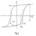
- fig. 1 shows a typical so-called ''hysteresis loop" of a ferroelectric material
- the polarization P of the ferroelectric material can be versus the electric field E and/or plotted with regard to a potential difference V.
- the value of the polarization will travel around the loop in the direction indicated.
- memory devices provided with capacitors comprising ferroelectric material will exhibit a memory effect in the absence of an applied external electric field, making it possible to store non-volatile data by applying a potential difference across the ferroelectric material, which evokes a polarization response.
- the direction (and magnitude) thereof may thus be set and left in a desired state.
- the polarization status can be determined. Storing and determining data will be described in more detail below.
- a nominal voltage V s employed for driving the polarization state of the ferroelectric material is typically selected considerably larger than the coercive voltage E c .
- the nominal voltage V s is generically illustrated with a dashed line in fig. 1, but is by no means limited to this particular value. Other values can be applicable.
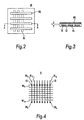
- Fig. 2 illustrates a portion of a m ⁇ n memory matrix 11 of a passive matrix memory 10 showing two mutually opposing sets of parallel electrodes, viz. word line electrodes WL and bit line electrodes BL.
- the word line and the bit line electrodes WL;BL are arranged perpendicular to each other, whereby they at the intersecting areas define side walls of specific volume elements of an insulating ferroelectric material (described in more detail below) and which in its turn define the volume of capacitor-like memory cells in the memory matrix 11.
- Fig. 3 discloses a cross-sectional view along line A-A in fig. 2.
- each "capacitor” is the ferroelectric material in a ferroelectric layer 12, where the thickness of the material defines the height h of the volume elements which in their turn define the memory cells 13. - For reasons of simplicity, only three crossing points between the word line and bit line electrodes WL;BL are illustrated in fig. 2.
- the ferroelectric material in the cell 13 is subjected to an electric field E which evokes a polarization response, having a direction which may be set and left in one of two stable states, positive or negative polarization, according to what is disclosed for instance in fig. 1.
- the two states represent the binary states "1" and "0".
- the polarization status of the cell 13 may be altered or deduced by renewed application of a potential difference between the two opposing electrodes WL and BL addressing that cell 13, which either causes the polarization to remain unchanged after removal of the potential difference, or to flip to the opposite direction.
- the polarization change causes a large current.
- the current is compared to a reference which can be provided in a number of ways (not shown) to be able to decide whether a "0" or a "1" is present. If the read is a destructive read, the polarization state in some of the cells will be switched to the opposite state. For instance can the polarization state of the cell be switched to "0" whether it is the state "1” or the state "0" that is read. The initial state must be written back to a cell in the memory to keep the information in the memory , i.e. the readout value.
- a more detailed description of how a passive matrix memory operates will be given in below when describing a preferred embodiment of the invention.
- fig. 4 illustrating another readout method for passive matrix memories, hereinafter called “full word read”, whereby an active word line, herein the first word line WL 1 comprising a desired memory cell 13, is sensed over its entire word length, that is, each of the memory cells 13 defined by the bit lines BL 1 ,...BL n .
- Full word read per se is a known concept described for instance in US-A-6 157 578.
- the solution is directed to an active matrix memory device, with the purpose of increasing the speed of transferring data stored in a relatively large block of a memory matrix.
- the present invention is on the contrary related to passive matrix memories, whereby prior art knowledge regarding active matrices, such as described in US-A-6 157 578, is not relevant since active devices does not have the problem with disturbing non-addressed cells.
- the active word line in this case the first word line WL 1
- the sensing means can for instance be sense amplifiers.
- the full word read method offers several advantages. For instance may the readout voltage be chosen much higher than the coercive voltage without incurring partial switching in non-addressed cells, and the method is compatible with a large matrix.
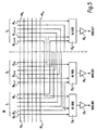
- the matrix proper is embodied as an m ⁇ n matrix formed by m word lines WL 1,...m and n bit lines BL 1,...n .
- the word lines are divided in q segments S, each segment S being defined by a number k adjacent bit lines BL in the matrix BL.
- the first bit line in each segment S can now be coupled by a first multiplexer 25 1 to a first sensing means 26 1 .
- the second bit line in each segment shall correspondingly be coupled to another multiplexer 25 2 , such that k'th line in each segment will be coupled to last multiplexer 25 k .
- the number of multiplexers (MUX) 25 shall in other words shall be equal to the largest number of bit lines BL which defines a segment. It is, of course, nothing that prevents that the number of bit lines in each segment S can be different, but if the memory cells on the bit lines on the segment contain data words with the same length, k will be the same for all segments.
- Each multiplexer 25 is connected with a sensing means 26 for readout of data and the number of sensing means 26 will hence also be equal to the largest number k bit lines BL which defines a segment.
- all the memory cells 13 in a word line segment n is connected simultaneously to the sensing means 26 such that all bit spots on a word line segment can be read out in parallel.
- the sensing means be sense amplifiers.
- - Data which are stored and/or shall be stored in the memory matrix 11 can be accessed by means of an associated row decoder and column decoder which is not shown in fig. 5 and the data which is stored in the memory cells 13 in the memory matrix 11 can be read out with a pulse protocol, e.g. as discussed in connection with fig.
- All bit lines BL which define a word line segment S are routed to multiplexers 25 and are selected only when a given word line WL in this segment is active. In this manner all bit lines in the active word line WL in the segment S is read out in parallel in a "full word configuration" and all bit lines are distributed among the sense amplifiers 26.
- Other architectures are of course, also possible, e.g. with 9, 16 or 32 bit lines in each segment S.
- At least 256 memory cells 13 are used in each segment S. With the use of a 32:1 multiplexers 25 this forms 8192 bits wide memory with only 32 duplication of word line drivers. Each word line will, of course, be segmented according to the number of provided sense amplifiers 26.
- FIG. 6 there is shown an alternative embodiment of the memory device according to the present invention, wherein the multiplexers are replaced by gate means 25.
- the gate means 25 activate the bit lines BL in the same manner as the multiplexers.
- the gate means 25 are realized as pass gates connected with each bit line BL in a segment S. While the number of multiplexers 25 in the embodiment in fig. 5 shall be equal to the number of bit lines BL in the segment S, namely k, the number of pass gates 25 in the embodiment in fig. 6 shall correspond to the number q of segments S. The number of outputs on each pass gate 25 corresponds to the number of bit lines BL in the respective segment S.
- a sense amplifier 26 is used for each bit line BL in the segment, each sense amplifier 26 being connected to one of the lines 27 on a data bus 28.
- a first output of the pass gate is connected to the first bus line 27 1 and the second to the second bus line 27 2 etc. and the number of bus lines 27 and sense amplifiers will, of course, be the greatest number of bit lines BL which defines a segment S.
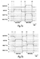
- Figs. 7a and 7b render alternative timing diagrams for a full word read cycle.
- Fig. 7a shows a timing diagram for full word read with a following write/read cycle ("refresh", "write back") for a word line segment.
- This timing diagram is based on a four-level voltage protocol. According to this timing diagram all word lines and all bit lines are, when no cell in the matrix is read or written, kept at a quiescent voltage equal to zero volts. All memory cells have an address which represent the crossings formed of an activated word line WL and by all bit lines BL within this segment which is to be read.
- the inactive word lines WL and all bit lines BL follow the same potential curves during the read cycle.
- the word line contacting the cells to be read is set to switching voltage V s .
- all bit lines are kept at zero voltage.
- V s switching voltage
- all cells on the active word lines are set to the zero state after the read operation has been performed. Therefore, in order to restore data stored in the memory, it will be necessary to write back "1" only on the bit lines which has cells that should contain "1". This is shown in both examples in figures 7a and 7b, where a voltage with reversed polarity is applied to the cell which shall be written with "1" during the read cycle as indicated in the diagram.
- Fig. 7b illustrates an alternate timing diagram based on a four-level voltage protocol. According to this embodiment all word lines and bit lines, when no cell in the matrix is read or written, are kept at a quiescent voltage V s /3.
- the word lines could in principle be uninterrupted, i.e. that they are extending continuously to the separate segments, the segments only being defined by the bit lines in question. Multiplexing and protocols for read and write must then be adapted thereto. It is, however, no advantage that the word lines become too long. With a limited number of segments and a limited number of bit lines in each segments this is avoided, e.g. as in the above mentioned example, where 256 000 word lines and 8 segments with 8 bit lines in each segment are used. The memory then obtains as stated a storage capacity of 16 Mbits. There are, however, also other disadvantages with continuous word lines.
- the same high voltage will be impressed on the active word line in all segments and even though only the bit lines in the addressed segments are connected, capacitive couplings and sneak currents can be formed and influence e.g. the memory cells in adjacent non-active word lines in the segment, something which may lead to spurious readouts or noise contributions.
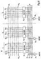
- it will hence be relevant also to be able to segment the word lines electrically such that only the active word line within the addressed segment is connected electrically to the driver, while the corresponding word line segments in the remaining segments are disconnected. This will particularly be relevant when the protocol in fig.
- a not shown driver in a driver group 20 is selected by means of a segment selector 22 which e.g. may be realized as a selector bus, such that the word line WL in the selected segment S is activated for a read or write cycle.
- the multiplexers 25 which are controlled by the segment selector means 22 can be connected with a selected driver in the group 20 via switches 24 and controlled via the selector means 22 over a switchable cache memory 21.
- the specific multiplexer 25 is simultaneously addressed for connecting the bit lines BL in the addressed segment to the sense amplifier 26.
- each word line WL in a segment can be connected to an AND gate, e.g. a CMOS logic gate or a pass gate, and the segment be addressed from a word line or address decoder. For instance the word line WL 1 is selected in the segment S 1 and it is then voltage only on this word line within the segment S 1 . With destructive readout now all memory cells and the word lines WL 1 in the segment S 1 will be switched to zero state, while the multiplexer 25 connects all bit lines in the segment S 1 to the respective sense amplifiers 26 1 ...26 k . All cells on the activated word line can hence be read out, i.e. a full word read is obtained if the word line of the segment is defined to contain a data word.
- an AND gate e.g. a CMOS logic gate or a pass gate
- the remaining word lines WL 2 ...WL m and bit lines BL 1 -BL k is kept on a quiescent voltage near the biasing points of the sense amplifiers 26 and in principle there will then be no disturbance contribution from the remaining cells of the segment. Neither will there be any bias voltage on the cells on the bit line, such that disturbing signals to the input of the sense amplifiers 26 can be generated.
- the data output of the sense amplifier 26 is conveyed to a two-way data bus 23 while a write logic 29 is connected in parallel on the output of the multiplexers for writing of data to the bit spots of the cells on an active word line in the segment, the word lines in the segments being selected in corresponding ways via the selector means 22 as in case of readout.
- a write logic 29 is connected in parallel on the output of the multiplexers for writing of data to the bit spots of the cells on an active word line in the segment, the word lines in the segments being selected in corresponding ways via the selector means 22 as in case of readout.
- buffer memories 21 on the switchable outputs of the selector means 22 and the latter connect drivers and multiplexers 25 via a number of line switches 24 controlled by the selector means 22.
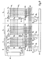
- Fig. 9 shows an embodiment functionally equivalent to that of fig. 8, but which additionally corresponds to the embodiment in fig. 6 wherein the multiplexers have been replaced by pass means 25.
- Each pass means 25 can e.g. comprise switching transistors 25a which function as pass gates, one for each line such that there will be a total of k switching transistors 25a in a pass means 25.
- driver groups 20 are provided, one for each segment, while the selector means 22 now is replaced by a driver group selector 22a.
- the addressing of the separate word line WL takes place over the output in a word line address bus 30 under control by the group selector 22a.
- bit lines 25a are connected to the bus line 27 in the data bus 28 and the data output of the sense amplifier is connected with a two-way data bus 23.
- the write logic 29 is provided in parallel over the sense amplifiers 26 and when writing takes place, the word line segment is selected via the group selectors 22a and with addressing over the word line address bus 30.
- the number of voltage levels and the voltage levels themselves in the pulsing protocol can be selected arbitrarily as long as the requirements for performing full word read are met. Further, the polarity of the voltages according to the protocols shown may as well be reversed.
- the memory matrix can be provided on a substrate and word line drivers integrated therein, such that the total area of the device does not increase.
- the segmented word lines could as well be implemented on stacked memory planes, with the bit lines BL connected vertically to the multiplexers or gate means 25.
- This is illustrated in fig. 10, which shows schematically and in cross section an embodiment wherein memory devices 10 according to the invention are provided in a stacked arrangement.
- each layer or memory plane P comprises one memory device 10.
- the respective word lines and bit lines can be connected over so-called staggered vias, i.e. alternating horizontal and vertical "over-the-edge" connections with driver and control circuitry in the substrate 14.
- the substrate 14 can be inorganic, i.e. silicon-based, and hence the circuitry may be implemented in e.g.
- FIG. 8 shows only two memory planes P 1 ,P 2 (note that only a limited number of bit lines are shown), but in practice the volumetric data storage apparatus may comprise a very large number of memory planes, from 8 and well beyond 100 or more, realizing a memory with very high capacity and storage density, as each memory plane only will be about 1 ⁇ m thick or even less.
- the memory device of the invention can be realized with a reduced number of sense amplifiers, which is an advantage when the memory is large and also with regard to the power consumption of the sense amplifiers. This can be high, but may also be reduced to some extent by appropriate power management of the driving and addressing circuitry. Moreover, a reduction in the number of sense amplifiers implies that real estate devoted to sense means can be balanced to achieve overall area optimization in the memory device. Finally, the segmentation of the word lines implies that errors during readout or addressing will be located in a single word in the event of a single word line fault.
Landscapes
- Engineering & Computer Science (AREA)
- Computer Hardware Design (AREA)
- Semiconductor Memories (AREA)
- Dram (AREA)
- Read Only Memory (AREA)
- Measurement Of Length, Angles, Or The Like Using Electric Or Magnetic Means (AREA)
- Magnetic Record Carriers (AREA)
- Pharmaceuticals Containing Other Organic And Inorganic Compounds (AREA)
- Peptides Or Proteins (AREA)
- Internal Circuitry In Semiconductor Integrated Circuit Devices (AREA)
- Investigating Or Analysing Biological Materials (AREA)
- Investigating Or Analyzing Materials By The Use Of Fluid Adsorption Or Reactions (AREA)
- Investigating Or Analysing Materials By The Use Of Chemical Reactions (AREA)
Applications Claiming Priority (3)
| Application Number | Priority Date | Filing Date | Title |
|---|---|---|---|
| NO20004236A NO20004236L (no) | 2000-08-24 | 2000-08-24 | Ikke-flyktig passiv matriseinnretning og fremgangsmåte for utlesing av samme |
| NO20004236 | 2000-08-24 | ||
| PCT/NO2001/000348 WO2002025665A2 (en) | 2000-08-24 | 2001-08-24 | Non-volatile passive matrix and method for readout of the same |
Publications (2)
| Publication Number | Publication Date |
|---|---|
| EP1316090A2 EP1316090A2 (en) | 2003-06-04 |
| EP1316090B1 true EP1316090B1 (en) | 2005-03-09 |
Family
ID=19911499
Family Applications (1)
| Application Number | Title | Priority Date | Filing Date |
|---|---|---|---|
| EP01985301A Expired - Lifetime EP1316090B1 (en) | 2000-08-24 | 2001-08-24 | Non-volatile passive matrix and method for readout of the same |
Country Status (14)
| Country | Link |
|---|---|
| US (1) | US20030137865A1 (enExample) |
| EP (1) | EP1316090B1 (enExample) |
| JP (1) | JP3848620B2 (enExample) |
| KR (1) | KR100540266B1 (enExample) |
| CN (1) | CN100530420C (enExample) |
| AT (1) | ATE290711T1 (enExample) |
| AU (2) | AU2002223159B2 (enExample) |
| CA (1) | CA2420378C (enExample) |
| DE (1) | DE60109307T2 (enExample) |
| DK (1) | DK1316090T3 (enExample) |
| ES (1) | ES2238053T3 (enExample) |
| NO (1) | NO20004236L (enExample) |
| RU (1) | RU2245584C2 (enExample) |
| WO (1) | WO2002025665A2 (enExample) |
Cited By (2)
| Publication number | Priority date | Publication date | Assignee | Title |
|---|---|---|---|---|
| DE102016012071A1 (de) | 2016-10-10 | 2018-04-12 | Kai-Uwe Demasius | Matrix mit kapazitiver Steuerungsvorrichtung |
| WO2018069359A1 (de) | 2016-10-10 | 2018-04-19 | Demasius Kai Uwe | Kapazitive matrixanordnung und verfahren zu deren ansteuerung |
Families Citing this family (25)
| Publication number | Priority date | Publication date | Assignee | Title |
|---|---|---|---|---|
| US6756620B2 (en) * | 2001-06-29 | 2004-06-29 | Intel Corporation | Low-voltage and interface damage-free polymer memory device |
| US6624457B2 (en) | 2001-07-20 | 2003-09-23 | Intel Corporation | Stepped structure for a multi-rank, stacked polymer memory device and method of making same |
| NO314524B1 (no) * | 2001-11-30 | 2003-03-31 | Thin Film Electronics Asa | Fremgangsmåte til lesing av celler i en passiv matriseadresserbar innretning, samt innretning for utförelse av fremgangsmåten |
| US6996652B1 (en) * | 2002-09-19 | 2006-02-07 | Inapac Technology, Inc. | High-speed segmented data bus architecture |
| NO324607B1 (no) * | 2003-11-24 | 2007-11-26 | Thin Film Electronics Asa | Fremgangsmate for a betjene et datalagringsapparat som benytter passiv matriseadressering |
| KR100576484B1 (ko) * | 2003-12-09 | 2006-05-10 | 주식회사 하이닉스반도체 | 차동 데이터를 가지는 불휘발성 강유전체 메모리 장치 |
| NO324029B1 (no) * | 2004-09-23 | 2007-07-30 | Thin Film Electronics Asa | Lesemetode og deteksjonsanordning |
| CN100466036C (zh) * | 2005-06-30 | 2009-03-04 | 精工爱普生株式会社 | 显示装置及电子设备 |
| TWI260643B (en) | 2005-12-30 | 2006-08-21 | Ind Tech Res Inst | Organic memory |
| CN1996495B (zh) * | 2005-12-31 | 2010-11-03 | 财团法人工业技术研究院 | 有机存储器之位单元 |
| CN1996486B (zh) * | 2005-12-31 | 2010-11-03 | 财团法人工业技术研究院 | 数字感测电路 |
| CN100524519C (zh) * | 2005-12-31 | 2009-08-05 | 财团法人工业技术研究院 | 有机存储器 |
| ES2301344B1 (es) * | 2006-03-14 | 2009-05-01 | Universidad De Zaragoza | Sistema de comunicaciones digitales para entornos residenciales, asistenciales, oficinas y similares. |
| EP1944763A1 (en) * | 2007-01-12 | 2008-07-16 | STMicroelectronics S.r.l. | Reading circuit and method for data storage system |
| US9574326B2 (en) | 2012-08-02 | 2017-02-21 | Harnischfeger Technologies, Inc. | Depth-related help functions for a shovel training simulator |
| AU2014202349A1 (en) | 2012-08-02 | 2014-05-22 | Harnischfeger Technologies, Inc. | Depth-related help functions for a wheel loader training simulator |
| JP5714681B2 (ja) * | 2013-10-25 | 2015-05-07 | ウィンボンド エレクトロニクス コーポレーション | 半導体記憶装置 |
| US9773553B1 (en) * | 2016-08-19 | 2017-09-26 | Micron Technology, Inc. | Segmented memory and operation |
| JP2020088497A (ja) * | 2018-11-20 | 2020-06-04 | 三星電子株式会社Samsung Electronics Co.,Ltd. | メモリ回路、半導体装置および移動体デバイス |
| US11102437B2 (en) | 2018-11-20 | 2021-08-24 | Samsung Electronics Co., Ltd. | Memory circuit and semiconductor device |
| US12407532B2 (en) * | 2020-02-18 | 2025-09-02 | International Business Machines Corporation | Gain cell memory based physically unclonable function |
| KR20210143612A (ko) * | 2020-05-20 | 2021-11-29 | 삼성전자주식회사 | 비휘발성 메모리 및 비휘발성 메모리의 동작 방법 |
| CN111696602A (zh) * | 2020-05-22 | 2020-09-22 | 珠海拍字节信息科技有限公司 | 铁电存储器及其操作方法 |
| US11309034B2 (en) * | 2020-07-15 | 2022-04-19 | Ferroelectric Memory Gmbh | Memory cell arrangement and methods thereof |
| CN114093398A (zh) * | 2021-11-26 | 2022-02-25 | 无锡拍字节科技有限公司 | 一种铁电存储器的位线布局及铁电存储器 |
Family Cites Families (14)
| Publication number | Priority date | Publication date | Assignee | Title |
|---|---|---|---|---|
| US4599709A (en) * | 1984-02-17 | 1986-07-08 | At&T Bell Laboratories | Byte organized static memory |
| SU1378682A1 (ru) * | 1986-05-18 | 1994-12-30 | В.И. Овчаренко | Матричный накопитель для постоянного запоминающего устройства |
| SU1596392A1 (ru) * | 1987-10-23 | 1990-09-30 | Предприятие П/Я Х-5737 | Матричный накопитель и способ управлени записью, считыванием и стиранием информации в накопителе |
| DE68923573T2 (de) * | 1988-03-31 | 1996-01-18 | Sony Corp | Eingangsschaltungen. |
| JP2982905B2 (ja) * | 1989-10-02 | 1999-11-29 | 三菱電機株式会社 | ダイナミック型半導体記憶装置 |
| US5086412A (en) * | 1990-11-21 | 1992-02-04 | National Semiconductor Corporation | Sense amplifier and method for ferroelectric memory |
| KR950011965B1 (ko) * | 1992-02-19 | 1995-10-12 | 삼성전자주식회사 | 불휘발성 반도체 메모리 장치 |
| TW231343B (enExample) * | 1992-03-17 | 1994-10-01 | Hitachi Seisakusyo Kk | |
| JPH0677434A (ja) * | 1992-08-27 | 1994-03-18 | Hitachi Ltd | 半導体記憶装置 |
| US5337414A (en) * | 1992-09-22 | 1994-08-09 | Unisys Corporation | Mass data storage and retrieval system |
| US5424997A (en) * | 1994-03-15 | 1995-06-13 | National Semiconductor Corporation | Non-volatile semiconductor memory having switching devices for segmentation of a memory page and a method thereof |
| US5567636A (en) * | 1995-02-27 | 1996-10-22 | Motorola Inc. | Process for forming a nonvolatile random access memory array |
| US5574692A (en) * | 1995-06-07 | 1996-11-12 | Lsi Logic Corporation | Memory testing apparatus for microelectronic integrated circuit |
| US5969380A (en) * | 1996-06-07 | 1999-10-19 | Micron Technology, Inc. | Three dimensional ferroelectric memory |
-
2000
- 2000-08-24 NO NO20004236A patent/NO20004236L/no not_active Application Discontinuation
-
2001
- 2001-08-24 AU AU2002223159A patent/AU2002223159B2/en not_active Ceased
- 2001-08-24 RU RU2003108726/09A patent/RU2245584C2/ru not_active IP Right Cessation
- 2001-08-24 DK DK01985301T patent/DK1316090T3/da active
- 2001-08-24 AT AT01985301T patent/ATE290711T1/de not_active IP Right Cessation
- 2001-08-24 JP JP2002529782A patent/JP3848620B2/ja not_active Expired - Fee Related
- 2001-08-24 CN CNB018178707A patent/CN100530420C/zh not_active Expired - Fee Related
- 2001-08-24 CA CA002420378A patent/CA2420378C/en not_active Expired - Fee Related
- 2001-08-24 AU AU2315902A patent/AU2315902A/xx active Pending
- 2001-08-24 DE DE60109307T patent/DE60109307T2/de not_active Expired - Lifetime
- 2001-08-24 ES ES01985301T patent/ES2238053T3/es not_active Expired - Lifetime
- 2001-08-24 KR KR1020037002558A patent/KR100540266B1/ko not_active Expired - Fee Related
- 2001-08-24 EP EP01985301A patent/EP1316090B1/en not_active Expired - Lifetime
- 2001-08-24 WO PCT/NO2001/000348 patent/WO2002025665A2/en not_active Ceased
- 2001-09-24 US US10/088,913 patent/US20030137865A1/en not_active Abandoned
Cited By (3)
| Publication number | Priority date | Publication date | Assignee | Title |
|---|---|---|---|---|
| DE102016012071A1 (de) | 2016-10-10 | 2018-04-12 | Kai-Uwe Demasius | Matrix mit kapazitiver Steuerungsvorrichtung |
| WO2018069359A1 (de) | 2016-10-10 | 2018-04-19 | Demasius Kai Uwe | Kapazitive matrixanordnung und verfahren zu deren ansteuerung |
| US10504575B2 (en) | 2016-10-10 | 2019-12-10 | Kai-Uwe Demasius | Capacitive matrix arrangement and method for actuation thereof |
Also Published As
| Publication number | Publication date |
|---|---|
| CN1471712A (zh) | 2004-01-28 |
| CA2420378C (en) | 2006-05-09 |
| NO20004236L (no) | 2002-02-25 |
| AU2002223159B2 (en) | 2005-04-14 |
| JP3848620B2 (ja) | 2006-11-22 |
| WO2002025665A2 (en) | 2002-03-28 |
| JP2004510283A (ja) | 2004-04-02 |
| AU2315902A (en) | 2002-04-02 |
| DK1316090T3 (da) | 2005-05-30 |
| ES2238053T3 (es) | 2005-08-16 |
| EP1316090A2 (en) | 2003-06-04 |
| DE60109307T2 (de) | 2006-04-13 |
| KR100540266B1 (ko) | 2006-01-10 |
| CN100530420C (zh) | 2009-08-19 |
| NO20004236D0 (no) | 2000-08-24 |
| KR20030059110A (ko) | 2003-07-07 |
| RU2245584C2 (ru) | 2005-01-27 |
| ATE290711T1 (de) | 2005-03-15 |
| WO2002025665A3 (en) | 2002-05-16 |
| US20030137865A1 (en) | 2003-07-24 |
| CA2420378A1 (en) | 2002-03-28 |
| DE60109307D1 (de) | 2005-04-14 |
Similar Documents
| Publication | Publication Date | Title |
|---|---|---|
| EP1316090B1 (en) | Non-volatile passive matrix and method for readout of the same | |
| AU2002223159A1 (en) | Non-volatile passive matrix and method for readout of the same | |
| US6301145B1 (en) | Ferroelectric memory and method for accessing same | |
| CN1118826C (zh) | 具有基准单元阵列块的铁电随机存取存储器器件 | |
| JP3753331B2 (ja) | 強誘電体メモリ装置 | |
| US5991188A (en) | Non-volatile ferroelectric memory with section plate line drivers and method for accessing the same | |
| US6154387A (en) | Semiconductor memory device utilizing a polarization state of a ferroelectric film | |
| CN1146997C (zh) | 具有多个存储体的数据存储器 | |
| KR20030066378A (ko) | 메모리 장치 및 메모리 시스템 | |
| US7212430B2 (en) | Semiconductor memory | |
| US20020024835A1 (en) | Non-volatile passive matrix device and method for readout of the same | |
| JP3970846B2 (ja) | 強誘電体メモリにおける読み取り信号の増強 | |
| KR20040028738A (ko) | 강유전체 메모리 및 그 동작 방법 | |
| EP0741388B1 (en) | Ferro-electric memory array architecture and method for forming the same | |
| CN1271944A (zh) | 在单元区域的两对边布置有读放大器的集成存储器 | |
| HK1062073A (en) | Non-volatile passive matrix and method for readout of the same | |
| KR100314472B1 (ko) | 강유전체 메모리 | |
| JP3945498B2 (ja) | メモリセル及び半導体記憶装置 | |
| NO318368B1 (no) | Ikke-flyktig passiv matriseinnretning og fremgangsmate for utlesing av samme | |
| JP4125743B2 (ja) | 強誘電体メモリ装置 | |
| JP2008016120A (ja) | 強誘電体メモリ装置 | |
| KR20010003223A (ko) | 강유전체 랜덤 억세스 메모리 장치 및 그의 기입 방법 | |
| JP2006236443A (ja) | 強誘電体メモリ装置 |
Legal Events
| Date | Code | Title | Description |
|---|---|---|---|
| PUAI | Public reference made under article 153(3) epc to a published international application that has entered the european phase |
Free format text: ORIGINAL CODE: 0009012 |
|
| 17P | Request for examination filed |
Effective date: 20030321 |
|
| AK | Designated contracting states |
Designated state(s): AT BE CH CY DE DK ES FI FR GB GR IE IT LI LU MC NL PT SE TR |
|
| AX | Request for extension of the european patent |
Extension state: AL LT LV MK RO SI |
|
| 17Q | First examination report despatched |
Effective date: 20031110 |
|
| GRAP | Despatch of communication of intention to grant a patent |
Free format text: ORIGINAL CODE: EPIDOSNIGR1 |
|
| GRAS | Grant fee paid |
Free format text: ORIGINAL CODE: EPIDOSNIGR3 |
|
| GRAA | (expected) grant |
Free format text: ORIGINAL CODE: 0009210 |
|
| AK | Designated contracting states |
Kind code of ref document: B1 Designated state(s): AT BE CH CY DE DK ES FI FR GB GR IE IT LI LU MC NL PT SE TR |
|
| PG25 | Lapsed in a contracting state [announced via postgrant information from national office to epo] |
Ref country code: AT Free format text: LAPSE BECAUSE OF FAILURE TO SUBMIT A TRANSLATION OF THE DESCRIPTION OR TO PAY THE FEE WITHIN THE PRESCRIBED TIME-LIMIT Effective date: 20050309 Ref country code: TR Free format text: LAPSE BECAUSE OF FAILURE TO SUBMIT A TRANSLATION OF THE DESCRIPTION OR TO PAY THE FEE WITHIN THE PRESCRIBED TIME-LIMIT Effective date: 20050309 |
|
| REG | Reference to a national code |
Ref country code: GB Ref legal event code: FG4D |
|
| REG | Reference to a national code |
Ref country code: CH Ref legal event code: EP |
|
| REG | Reference to a national code |
Ref country code: IE Ref legal event code: FG4D |
|
| REF | Corresponds to: |
Ref document number: 60109307 Country of ref document: DE Date of ref document: 20050414 Kind code of ref document: P |
|
| REG | Reference to a national code |
Ref country code: SE Ref legal event code: TRGR |
|
| REG | Reference to a national code |
Ref country code: DK Ref legal event code: T3 |
|
| PG25 | Lapsed in a contracting state [announced via postgrant information from national office to epo] |
Ref country code: GR Free format text: LAPSE BECAUSE OF FAILURE TO SUBMIT A TRANSLATION OF THE DESCRIPTION OR TO PAY THE FEE WITHIN THE PRESCRIBED TIME-LIMIT Effective date: 20050609 |
|
| REG | Reference to a national code |
Ref country code: CH Ref legal event code: NV Representative=s name: RITSCHER & PARTNER AG |
|
| REG | Reference to a national code |
Ref country code: ES Ref legal event code: FG2A Ref document number: 2238053 Country of ref document: ES Kind code of ref document: T3 |
|
| PG25 | Lapsed in a contracting state [announced via postgrant information from national office to epo] |
Ref country code: IE Free format text: LAPSE BECAUSE OF NON-PAYMENT OF DUE FEES Effective date: 20050824 Ref country code: CY Free format text: LAPSE BECAUSE OF FAILURE TO SUBMIT A TRANSLATION OF THE DESCRIPTION OR TO PAY THE FEE WITHIN THE PRESCRIBED TIME-LIMIT Effective date: 20050824 Ref country code: LU Free format text: LAPSE BECAUSE OF NON-PAYMENT OF DUE FEES Effective date: 20050824 |
|
| PG25 | Lapsed in a contracting state [announced via postgrant information from national office to epo] |
Ref country code: MC Free format text: LAPSE BECAUSE OF NON-PAYMENT OF DUE FEES Effective date: 20050831 |
|
| PG25 | Lapsed in a contracting state [announced via postgrant information from national office to epo] |
Ref country code: PT Free format text: LAPSE BECAUSE OF FAILURE TO SUBMIT A TRANSLATION OF THE DESCRIPTION OR TO PAY THE FEE WITHIN THE PRESCRIBED TIME-LIMIT Effective date: 20050907 |
|
| PLBE | No opposition filed within time limit |
Free format text: ORIGINAL CODE: 0009261 |
|
| STAA | Information on the status of an ep patent application or granted ep patent |
Free format text: STATUS: NO OPPOSITION FILED WITHIN TIME LIMIT |
|
| 26N | No opposition filed |
Effective date: 20051212 |
|
| ET | Fr: translation filed | ||
| REG | Reference to a national code |
Ref country code: IE Ref legal event code: MM4A |
|
| PGFP | Annual fee paid to national office [announced via postgrant information from national office to epo] |
Ref country code: DK Payment date: 20070829 Year of fee payment: 7 |
|
| PGFP | Annual fee paid to national office [announced via postgrant information from national office to epo] |
Ref country code: ES Payment date: 20070917 Year of fee payment: 7 |
|
| PGFP | Annual fee paid to national office [announced via postgrant information from national office to epo] |
Ref country code: CH Payment date: 20070830 Year of fee payment: 7 Ref country code: FI Payment date: 20070830 Year of fee payment: 7 |
|
| PGFP | Annual fee paid to national office [announced via postgrant information from national office to epo] |
Ref country code: IT Payment date: 20070830 Year of fee payment: 7 Ref country code: NL Payment date: 20070823 Year of fee payment: 7 Ref country code: SE Payment date: 20070829 Year of fee payment: 7 |
|
| PGFP | Annual fee paid to national office [announced via postgrant information from national office to epo] |
Ref country code: BE Payment date: 20071012 Year of fee payment: 7 |
|
| REG | Reference to a national code |
Ref country code: CH Ref legal event code: PCAR Free format text: RITSCHER & PARTNER AG;RESIRAIN 1;8125 ZOLLIKERBERG (CH) |
|
| REG | Reference to a national code |
Ref country code: GB Ref legal event code: 732E Free format text: REGISTERED BETWEEN 20090212 AND 20090218 |
|
| REG | Reference to a national code |
Ref country code: DK Ref legal event code: EBP |
|
| REG | Reference to a national code |
Ref country code: CH Ref legal event code: PL |
|
| EUG | Se: european patent has lapsed | ||
| NLV4 | Nl: lapsed or anulled due to non-payment of the annual fee |
Effective date: 20090301 |
|
| PG25 | Lapsed in a contracting state [announced via postgrant information from national office to epo] |
Ref country code: FI Free format text: LAPSE BECAUSE OF NON-PAYMENT OF DUE FEES Effective date: 20080824 Ref country code: NL Free format text: LAPSE BECAUSE OF NON-PAYMENT OF DUE FEES Effective date: 20090301 |
|
| PG25 | Lapsed in a contracting state [announced via postgrant information from national office to epo] |
Ref country code: CH Free format text: LAPSE BECAUSE OF NON-PAYMENT OF DUE FEES Effective date: 20080831 Ref country code: LI Free format text: LAPSE BECAUSE OF NON-PAYMENT OF DUE FEES Effective date: 20080831 |
|
| PG25 | Lapsed in a contracting state [announced via postgrant information from national office to epo] |
Ref country code: DK Free format text: LAPSE BECAUSE OF NON-PAYMENT OF DUE FEES Effective date: 20080831 Ref country code: BE Free format text: LAPSE BECAUSE OF NON-PAYMENT OF DUE FEES Effective date: 20080831 |
|
| REG | Reference to a national code |
Ref country code: FR Ref legal event code: TP Ref country code: FR Ref legal event code: CD Ref country code: FR Ref legal event code: CJ |
|
| PG25 | Lapsed in a contracting state [announced via postgrant information from national office to epo] |
Ref country code: IT Free format text: LAPSE BECAUSE OF NON-PAYMENT OF DUE FEES Effective date: 20080824 |
|
| REG | Reference to a national code |
Ref country code: ES Ref legal event code: FD2A Effective date: 20080825 |
|
| PG25 | Lapsed in a contracting state [announced via postgrant information from national office to epo] |
Ref country code: ES Free format text: LAPSE BECAUSE OF NON-PAYMENT OF DUE FEES Effective date: 20080825 |
|
| PG25 | Lapsed in a contracting state [announced via postgrant information from national office to epo] |
Ref country code: SE Free format text: LAPSE BECAUSE OF NON-PAYMENT OF DUE FEES Effective date: 20080825 |
|
| PGFP | Annual fee paid to national office [announced via postgrant information from national office to epo] |
Ref country code: DE Payment date: 20100804 Year of fee payment: 10 Ref country code: FR Payment date: 20100819 Year of fee payment: 10 |
|
| PGFP | Annual fee paid to national office [announced via postgrant information from national office to epo] |
Ref country code: GB Payment date: 20100805 Year of fee payment: 10 |
|
| GBPC | Gb: european patent ceased through non-payment of renewal fee |
Effective date: 20110824 |
|
| REG | Reference to a national code |
Ref country code: FR Ref legal event code: ST Effective date: 20120430 |
|
| REG | Reference to a national code |
Ref country code: DE Ref legal event code: R119 Ref document number: 60109307 Country of ref document: DE Effective date: 20120301 |
|
| PG25 | Lapsed in a contracting state [announced via postgrant information from national office to epo] |
Ref country code: GB Free format text: LAPSE BECAUSE OF NON-PAYMENT OF DUE FEES Effective date: 20110824 Ref country code: FR Free format text: LAPSE BECAUSE OF NON-PAYMENT OF DUE FEES Effective date: 20110831 |
|
| PG25 | Lapsed in a contracting state [announced via postgrant information from national office to epo] |
Ref country code: DE Free format text: LAPSE BECAUSE OF NON-PAYMENT OF DUE FEES Effective date: 20120301 |